US5394100A - Probe system with automatic control of contact pressure and probe alignment - Google Patents
Probe system with automatic control of contact pressure and probe alignmentDownload PDFInfo
- Publication number
- US5394100A US5394100AUS08/058,573US5857393AUS5394100AUS 5394100 AUS5394100 AUS 5394100AUS 5857393 AUS5857393 AUS 5857393AUS 5394100 AUS5394100 AUS 5394100A
- Authority
- US
- United States
- Prior art keywords
- dut
- probe
- objective lens
- axis
- probe needle
- Prior art date
- Legal status (The legal status is an assumption and is not a legal conclusion. Google has not performed a legal analysis and makes no representation as to the accuracy of the status listed.)
- Expired - Fee Related
Links
Images
Classifications
- G—PHYSICS
- G01—MEASURING; TESTING
- G01R—MEASURING ELECTRIC VARIABLES; MEASURING MAGNETIC VARIABLES
- G01R31/00—Arrangements for testing electric properties; Arrangements for locating electric faults; Arrangements for electrical testing characterised by what is being tested not provided for elsewhere
- G01R31/28—Testing of electronic circuits, e.g. by signal tracer
- G01R31/302—Contactless testing
- G01R31/308—Contactless testing using non-ionising electromagnetic radiation, e.g. optical radiation
- G01R31/311—Contactless testing using non-ionising electromagnetic radiation, e.g. optical radiation of integrated circuits
- G—PHYSICS
- G01—MEASURING; TESTING
- G01R—MEASURING ELECTRIC VARIABLES; MEASURING MAGNETIC VARIABLES
- G01R1/00—Details of instruments or arrangements of the types included in groups G01R5/00 - G01R13/00 and G01R31/00
- G01R1/02—General constructional details
- G01R1/06—Measuring leads; Measuring probes
- G01R1/067—Measuring probes
- G01R1/073—Multiple probes
- G01R1/07307—Multiple probes with individual probe elements, e.g. needles, cantilever beams or bump contacts, fixed in relation to each other, e.g. bed of nails fixture or probe card
- G01R1/07314—Multiple probes with individual probe elements, e.g. needles, cantilever beams or bump contacts, fixed in relation to each other, e.g. bed of nails fixture or probe card the body of the probe being perpendicular to test object, e.g. bed of nails or probe with bump contacts on a rigid support
Definitions
- This inventionrelates to semiconductor probe systems, and more particularly, to an apparatus and method for automatically controlling contact pressure between a needle probe and a device under test.
- Probe systemsare employed to enable computer-controlled circuit testers to exercise various portions of circuitry contained within a device under test (DUT).
- DUTdevice under test
- a critical feature of a probe systemis an ability to accurately position needle probes in contact with pads on the DUT, with sufficient contact pressure to assure a reliable electrical connection.
- a probe cardwas set in place over a DUT in the view field of a stereo microscope. An operator observed the probe needle tips and controlled movable stages to bring both the DUT and probe needle tips into contact.
- Later wafer probe systemsincorporated automatic needle tip/wafer alignment systems that employed image recognition cameras.
- a probe systemin addition to assuring proper registration between probe tips and contact pads on a DUT, must control contact pressure between the contact pads and probe tips. If too little pressure is exerted, a high resistance connection may occur. If too much pressure is exerted, the wafer pad and/or probe tip may be damaged.
- a probe systemwhich employs a piezoelectric touch plate to determine the height (i.e., along a Z axis) of a group of probe tips in relation to a DUT support.
- Sato et al.employ a plurality of cameras to image various aspects of the probe tips and a DUT to enable X,Y dimension registration therebetween. Such imaging occurs from cameras positioned at disparate locations within the probe system and requires precise knowledge of the relative locations of the cameras. The probe tips and DUT are moved into registration subsequent to imaging.
- Such image recognition systemsare also employed to assure registration of layers of a semiconductor wafer (see U.S. Pat. No. 4,938,600 to Into).
- a probe system for probing a device under testincludes a DUT support chuck for holding the DUT.
- a plurality of flexible probe needlesare positioned along a "Z" axis that extends orthogonally from the surface of the DUT. Each probe needle is movable with respect to the DUT support chuck.
- a motorprovides for relative movement, at least along the Z axis, between the probe needles and the DUT support chuck.
- a variable focus imaging systemis positioned along the Z axis and provides image signals to a control processor. The control processor causes the variable focus imaging system to image the surface of the DUT and at least one probe needle.
- the control processoris responsive to a determined distance between focal planes containing the DUT surface and probe needle to cause the motor to move the probe needle and the DUT surface into physical engagement.
- the motoris further controlled to provide a relative movement distance between the probe needle and the DUT that is greater than the determined distance between the focal planes, thereby enabling a predetermined contact pressure to be obtained.
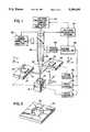
- FIG. 1is a schematic view of a system incorporating the invention.
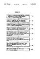
- FIG. 2is a logical flow diagram helpful in understanding the operation of the system of FIG. 1.
- FIG. 3shows a group of probe needles that extend from a probe support and are movable as a unit.
- DUT 10has been emplaced upon a device chuck 12.
- DUT 10may be a semiconductor wafer or chip having conductive pads that enable electrical access to internal active circuits. While not shown, DUT 10 is preferably held in a fixture which is, in turn, precisely positioned by a robot onto the upper surface of DUT chuck 12.
- a chuck control 14controls movement mechanisms associated with DUT chuck 12 that enable translational movement of DUT 10 in both the X, Y, and Z dimensions, as well as rotation about the Z axis.
- a pair of probe needles 16 and 18are positioned above the uppermost surface of DUT 10 and extend from probe supports 20, 22 and probe stages 24, 26, respectively.
- Each of probe stages 24 and 26is motor controlled and is translatable in the X, Y, and Z dimensions by respectively connected, stage control modules 28 and 30.
- DUT chuck 12, DUT 10 and needle probe tips 16, 18are all displaced along a Z-axis 32 that further defines the optical centerline of a microscope 34.
- An objective lens 36is motor driven by a focus motor 38 so as to enable movement of the focal plane of microscope 34 vertically along Z-axis 32. While objective lens 36 is illustrated as a single lens, those skilled in the art will understand that a set of lenses may also serve as objective lens 36. Further, it is important to understand that all imaging of this invention takes place through objective lens 36, thus obviating the need for a mechanically rotatable set of variable magnification objective lenses.
- a prism (or half silvered mirror) 40is positioned within microscope 34 and directs image light from objective lens 36 to both a focus camera 42 and a pattern recognition camera 44.
- Focus camera 42exhibits a narrow depth of field (DOF), e.g., 7-8 microns, and a small field of view (FOV), e.g., 1 mm.
- Focus camera 42preferably employs a charge coupled device (CCD) imager with internal optics that enable a relatively large magnification factor.
- pattern recognition camera 44exhibits a larger FOV (e.g. 2 mm) and a large DOF (e.g. 20 microns).
- Pattern recognition camera 44also preferably employs a CCD imager and exhibits a smaller degree of magnification than focus camera 42.
- Cameras 42 and 44provide inputs to a pattern recognition system 46 that enables imaged features to be identified and located within the FOV of either camera.
- a pattern recognition systemis commercially available and a preferred model is the Cognex 3000, from the Cognex Corporation, (insert remainder of address).
- the Cognex 3000is a processor-controlled, pattern recognition system that provides pattern data and autofocus inputs to a system controller 48.
- System controller 48is preferably a personal computer sized data processing system.
- FIG. 1Not shown in FIG. 1 are the electrical circuits connected to needle probes 16 and 18 that enable electrical stimulation to be applied to selected pads on the surface of DUT 10. Furthermore, the specific mechanisms that the control the positions of DUT chuck 12, and stages 24 and 26 have been excluded to avoid over complication of the view.
- the system of FIG. 1enables the upper surface of DUT 10 and the tips of probe needles 16 and 18 to be electronically imaged through a single objective lens 36.
- a Z-axis distanceis then determined between a focal plane that encompasses the uppermost surface of DUT 10 and a focal plane that encompasses a tip of a probe needle 16 or 18.
- the Z-axis determined distanceis added to an over-travel distance, with the sum being used to actuate a stage control (28 or 30) to move a probe needle (16 or 18) into contact with DUT 10 and to achieve a desired contact pressure.
- DUT 10is placed on DUT chuck 12 by a robot (not shown).
- Chuck control 14then brings DUT 10 into the FOV of pattern recognition camera 44.
- the approximate location of the pad to be imaged on the surface of DUT 10is preprogrammed into system controller 48, allowing DUT 10 to be moved in the X, Y, and Z dimensions by chuck control 14.
- pattern recognition camera 44images the upper surface of DUT 10 and locates the conductive pad thereon that is to be probed.
- pattern recognition system 46In order to enable pattern recognition camera 44 to move its focal plane to the upper surface of DUT 10, pattern recognition system 46, through system controller 48, causes focus motor 38 to move objective lens 36 until a proper level of focus is sensed. Similarly, when focus camera 42 comes into play, focus motor 38 is controlled to move the focal plane of the image presented to focus camera 42 until a properly focussed image is determined by pattern recognition system 46, at which point further movement of objective lens 36 by focus motor 30 ceases.
- the X and Y dimension positions of the pad to be probedare found by pattern recognition system 46 from the image provided by pattern recognition camera 44 and are fed to system controller 48 where they are stored. Focus camera 42 is now controlled to shift its focal plane to the located pad. This shift of focal plane is accomplished by focus motor 38 causing an appropriate shift in position of objective lens 36, using the Z dimensions of the DOF obtained from pattern recognition camera 44. Pattern recognition system 46 then controls focus camera 42 to bring the uppermost surface of the imaged pad into precise focus within the small DOF of focus camera 42. This action locates the precise Z-axis position of the uppermost surface of the pad, which position is fed by pattern recognition system 46 to system controller 48 (box 52).
- Pattern recognition camera 44is now focussed on a probe needle tip (e.g. either the tip of probe needle 16 or probe needle 18) and determines the tip's X and Y dimension locations (box 54).
- the Z axis DOF limits of pattern recognition camera 44are then fed by pattern recognition system 46 to system controller 48. Those Z axis limits are used to operate focus motor 30 to cause objective lens 36 to bring the focal plane of focus camera 42 into coincidence with the chosen probe needle tip.
- System controller 48now having Z-axis positions of the upper surface of DUT 10 and a probe tip, calculates a delta Z distance value between the probe tip and pad and adds an over-travel increment thereto. In this manner, a Z-Travel distance value is obtained (box 58).
- the over-travel incrementis a z-axis distance that, given the known flexibility of a probe needle, enables a desired level of contact pressure to be obtained between the tip and a pad.
- System controller 48next computes delta X and delta Y distances between the probe needle tip and the pad (box 60) and then causes a stage control (e.g. stage control 30) to move the respectively connected probe needle (e.g. 18) by the delta X and delta Y amounts and the by the Z-Travel distance value (box 62).
- stage controle.g. stage control 30
- the tip of probe needle 18contacts an imaged pad on the upper surface of DUT 10, in preparation for electrical stimulation thereof.
- the processis then repeated for probe needle 16 (box 64), at which point appropriate electrical stimuli is applied between probe needles 16 and 18 to enable testing of the circuitry within DUT 10.
- probe stages 24 and 26are shown as separately movable entities, a single card 70 with multiple probe needles 72 (see FIG. 3) may be moved into simultaneous contact with a plurality of pads on DUT 10. Under such conditions, only one stage control would be used to control the X, Y and Z movements of the connected probe card stage.
- the imaging systemmay use, in lieu of two imaging cameras, (1) a single camera with a motor operated zoom lens that enables automatic adjustment of DOF and FOV, or (2) a single focus camera in combination with multiple objective lenses mounted on a motor driven objective revolver. Accordingly, the present invention is intended to embrace all such alternatives, modifications and variances which fall within the scope of the appended claims.
Landscapes
- Engineering & Computer Science (AREA)
- Physics & Mathematics (AREA)
- General Physics & Mathematics (AREA)
- Computer Hardware Design (AREA)
- Microelectronics & Electronic Packaging (AREA)
- Health & Medical Sciences (AREA)
- Computer Vision & Pattern Recognition (AREA)
- Electromagnetism (AREA)
- Toxicology (AREA)
- General Engineering & Computer Science (AREA)
- Testing Or Measuring Of Semiconductors Or The Like (AREA)
Abstract
Description
Claims (8)
Priority Applications (1)
| Application Number | Priority Date | Filing Date | Title |
|---|---|---|---|
| US08/058,573US5394100A (en) | 1993-05-06 | 1993-05-06 | Probe system with automatic control of contact pressure and probe alignment |
Applications Claiming Priority (1)
| Application Number | Priority Date | Filing Date | Title |
|---|---|---|---|
| US08/058,573US5394100A (en) | 1993-05-06 | 1993-05-06 | Probe system with automatic control of contact pressure and probe alignment |
Publications (1)
| Publication Number | Publication Date |
|---|---|
| US5394100Atrue US5394100A (en) | 1995-02-28 |
Family
ID=22017665
Family Applications (1)
| Application Number | Title | Priority Date | Filing Date |
|---|---|---|---|
| US08/058,573Expired - Fee RelatedUS5394100A (en) | 1993-05-06 | 1993-05-06 | Probe system with automatic control of contact pressure and probe alignment |
Country Status (1)
| Country | Link |
|---|---|
| US (1) | US5394100A (en) |
Cited By (36)
| Publication number | Priority date | Publication date | Assignee | Title |
|---|---|---|---|---|
| US5642056A (en)* | 1993-12-22 | 1997-06-24 | Tokyo Electron Limited | Probe apparatus for correcting the probe card posture before testing |
| US5861759A (en)* | 1997-01-29 | 1999-01-19 | Tokyo Electron Limited | Automatic probe card planarization system |
| US5889582A (en)* | 1997-03-10 | 1999-03-30 | Virtek Vision Corporation | Image-directed active range finding system |
| US5952843A (en)* | 1998-03-24 | 1999-09-14 | Vinh; Nguyen T. | Variable contact pressure probe |
| US6002426A (en)* | 1997-07-02 | 1999-12-14 | Cerprobe Corporation | Inverted alignment station and method for calibrating needles of probe card for probe testing of integrated circuits |
| US6052189A (en)* | 1996-12-16 | 2000-04-18 | Fujitsu Limited | Height measurement device and height measurement method |
| US6150828A (en)* | 1994-04-18 | 2000-11-21 | Micron Technology, Inc. | Method and apparatus for automatically positioning electronic dice with component packages |
| US6313915B1 (en)* | 1998-08-27 | 2001-11-06 | Murata Manufacturing Co., Ltd. | Displacement measuring method and apparatus |
| WO2002003045A3 (en)* | 2000-06-30 | 2002-04-25 | Testship Automatic Test Soluti | Probe, systems and methods for integrated circuit board testing |
| US20020176095A1 (en)* | 2001-05-26 | 2002-11-28 | Stefan Dietrich | Imaging system and method for positioning a measuring tip onto a contact region of a microchip |
| US6545458B2 (en)* | 2000-03-30 | 2003-04-08 | Nagase Sangyo Kabushiki Kaisha | Low-temperature test equipment |
| US20040164758A1 (en)* | 2003-02-21 | 2004-08-26 | Nagar Mohan R. | Substrate impedance measurement |
| US20040251925A1 (en)* | 2003-05-30 | 2004-12-16 | Aritharan Thurairajaratnam | Measurement of package interconnect impedance using tester and supporting tester |
| US20050083038A1 (en)* | 2002-05-07 | 2005-04-21 | Atg Test Systems Gmbh & Co. Kg | Apparatus and method for the testing of circuit boards, and test probe for this apparatus and this method |
| US20050205778A1 (en)* | 2003-10-17 | 2005-09-22 | Gsi Lumonics Corporation | Laser trim motion, calibration, imaging, and fixturing techniques |
| US20060006891A1 (en)* | 2003-05-09 | 2006-01-12 | Atg Test Systems Gmbh & Co. Kg | Method for testing non-componented circuit boards |
| US20060290368A1 (en)* | 2003-05-06 | 2006-12-28 | Scorpion Technologies Ag | Circuit board test device comprising contact needles which are driven in diagonally protruding manner |
| US20070216431A1 (en)* | 2006-02-08 | 2007-09-20 | Bahadir Tunaboylu | Automated probe card planarization and alignment methods and tools |
| US20070236234A1 (en)* | 2005-04-06 | 2007-10-11 | Michael Huebner | Method and system for the optical inspection of contact faces at semiconductor devices with different appearances |
| US20080196474A1 (en)* | 2007-02-20 | 2008-08-21 | Centipede Systems, Inc. | Method and apparatus for aligning and/or leveling a test head |
| US20090058447A1 (en)* | 2007-08-27 | 2009-03-05 | Texas Instruments Incorporated | Fault analyzer |
| WO2009043752A1 (en)* | 2007-09-28 | 2009-04-09 | Siemens Aktiengesellschaft | Method and device for adjusting measuring probes |
| WO2009043654A1 (en)* | 2007-09-28 | 2009-04-09 | Siemens Aktiengesellschaft | Method for monitoring a measuring needle during test operation |
| EP2042878A3 (en)* | 2007-09-28 | 2009-04-22 | Siemens Aktiengesellschaft | Method for automatically aligning a number of measuring probe tips |
| US20090234502A1 (en)* | 2008-03-12 | 2009-09-17 | Denso Wave Incorporated | Apparatus for determining pickup pose of robot arm with camera |
| US20110013011A1 (en)* | 2006-12-27 | 2011-01-20 | Suss Microtec Test Systems Gmbh | Arrangement and method for focusing a multiplane image acquisition on a prober |
| US20110181710A1 (en)* | 2006-12-27 | 2011-07-28 | SUSS MicroTech Test Systems GmbH | Arrangement and method for image acquisition on a prober |
| WO2011113051A1 (en)* | 2010-03-12 | 2011-09-15 | Cascade Microtech, Inc. | System for testing semiconductors |
| US9110131B2 (en) | 2010-04-13 | 2015-08-18 | Cascade Microtech, Inc. | Method and device for contacting a row of contact areas with probe tips |
| CN104969080A (en)* | 2012-11-21 | 2015-10-07 | 康拉德有限责任公司 | Method and device for testing workpieces |
| US20190005639A1 (en)* | 2017-06-29 | 2019-01-03 | Seiko Epson Corporation | Electronic Component Handler And Electronic Component Tester |
| US10679335B2 (en) | 2017-07-31 | 2020-06-09 | Seiko Epson Corporation | Electronic component handler and electronic component tester |
| US11009541B2 (en) | 2017-06-29 | 2021-05-18 | Seiko Epson Corporation | Electronic component handler and electronic component tester |
| TWI769698B (en)* | 2021-02-08 | 2022-07-01 | 鴻勁精密股份有限公司 | Image taking apparatus and handler using the same |
| US11656181B2 (en) | 2018-12-21 | 2023-05-23 | Industrial Technology Research Institute | Inspection apparatus and inspection method for inspecting light-emitting diodes |
| US12203959B2 (en) | 2022-11-18 | 2025-01-21 | Formfactor, Inc. | Methods of establishing contact between a probe tip of a probe system and a device under test, probe systems that perform the methods, and storage media that directs probe systems to perform the methods |
Citations (8)
| Publication number | Priority date | Publication date | Assignee | Title |
|---|---|---|---|---|
| US4470074A (en)* | 1981-05-27 | 1984-09-04 | Dainippon Screen Mfg. Co., Ltd. | Method of scanning and recording images |
| US4677474A (en)* | 1984-07-02 | 1987-06-30 | Canon Kabushiki Kaisha | Wafer prober |
| US4786867A (en)* | 1986-09-02 | 1988-11-22 | Canon Kabushiki Kaisha | Wafer prober |
| US4920374A (en)* | 1986-05-19 | 1990-04-24 | Brother Kogyo Kabushiki Kaisha | Picture recording apparatus |
| US4929893A (en)* | 1987-10-06 | 1990-05-29 | Canon Kabushiki Kaisha | Wafer prober |
| US4938600A (en)* | 1989-02-09 | 1990-07-03 | Interactive Video Systems, Inc. | Method and apparatus for measuring registration between layers of a semiconductor wafer |
| US5091692A (en)* | 1990-01-11 | 1992-02-25 | Tokyo Electron Limited | Probing test device |
| USRE33883E (en)* | 1985-02-04 | 1992-04-14 | National Biomedical Research Foundation | Split-image multi-power microscopic image display system and method |
- 1993
- 1993-05-06USUS08/058,573patent/US5394100A/ennot_activeExpired - Fee Related
Patent Citations (8)
| Publication number | Priority date | Publication date | Assignee | Title |
|---|---|---|---|---|
| US4470074A (en)* | 1981-05-27 | 1984-09-04 | Dainippon Screen Mfg. Co., Ltd. | Method of scanning and recording images |
| US4677474A (en)* | 1984-07-02 | 1987-06-30 | Canon Kabushiki Kaisha | Wafer prober |
| USRE33883E (en)* | 1985-02-04 | 1992-04-14 | National Biomedical Research Foundation | Split-image multi-power microscopic image display system and method |
| US4920374A (en)* | 1986-05-19 | 1990-04-24 | Brother Kogyo Kabushiki Kaisha | Picture recording apparatus |
| US4786867A (en)* | 1986-09-02 | 1988-11-22 | Canon Kabushiki Kaisha | Wafer prober |
| US4929893A (en)* | 1987-10-06 | 1990-05-29 | Canon Kabushiki Kaisha | Wafer prober |
| US4938600A (en)* | 1989-02-09 | 1990-07-03 | Interactive Video Systems, Inc. | Method and apparatus for measuring registration between layers of a semiconductor wafer |
| US5091692A (en)* | 1990-01-11 | 1992-02-25 | Tokyo Electron Limited | Probing test device |
Cited By (63)
| Publication number | Priority date | Publication date | Assignee | Title |
|---|---|---|---|---|
| US5804983A (en)* | 1993-12-22 | 1998-09-08 | Tokyo Electron Limited | Probe apparatus with tilt correction mechanisms |
| US5642056A (en)* | 1993-12-22 | 1997-06-24 | Tokyo Electron Limited | Probe apparatus for correcting the probe card posture before testing |
| US6353312B1 (en) | 1994-04-18 | 2002-03-05 | Micron Technology, Inc. | Method for positioning a semiconductor die within a temporary package |
| US6492187B1 (en) | 1994-04-18 | 2002-12-10 | Micron Technology, Inc. | Method for automatically positioning electronic die within component packages |
| US6900459B2 (en) | 1994-04-18 | 2005-05-31 | Micron Technology, Inc. | Apparatus for automatically positioning electronic dice within component packages |
| US6150828A (en)* | 1994-04-18 | 2000-11-21 | Micron Technology, Inc. | Method and apparatus for automatically positioning electronic dice with component packages |
| US6210984B1 (en) | 1994-04-18 | 2001-04-03 | Micron Technology, Inc. | Method and apparatus for automatically positioning electronic dice within component packages |
| US6052189A (en)* | 1996-12-16 | 2000-04-18 | Fujitsu Limited | Height measurement device and height measurement method |
| US5861759A (en)* | 1997-01-29 | 1999-01-19 | Tokyo Electron Limited | Automatic probe card planarization system |
| US5889582A (en)* | 1997-03-10 | 1999-03-30 | Virtek Vision Corporation | Image-directed active range finding system |
| US6002426A (en)* | 1997-07-02 | 1999-12-14 | Cerprobe Corporation | Inverted alignment station and method for calibrating needles of probe card for probe testing of integrated circuits |
| US5952843A (en)* | 1998-03-24 | 1999-09-14 | Vinh; Nguyen T. | Variable contact pressure probe |
| US6313915B1 (en)* | 1998-08-27 | 2001-11-06 | Murata Manufacturing Co., Ltd. | Displacement measuring method and apparatus |
| US6545458B2 (en)* | 2000-03-30 | 2003-04-08 | Nagase Sangyo Kabushiki Kaisha | Low-temperature test equipment |
| WO2002003045A3 (en)* | 2000-06-30 | 2002-04-25 | Testship Automatic Test Soluti | Probe, systems and methods for integrated circuit board testing |
| US6842260B2 (en)* | 2001-05-26 | 2005-01-11 | Infineon Technologies Ag | Imaging system and method for positioning a measuring tip onto a contact region of a microchip |
| US20020176095A1 (en)* | 2001-05-26 | 2002-11-28 | Stefan Dietrich | Imaging system and method for positioning a measuring tip onto a contact region of a microchip |
| US20050083038A1 (en)* | 2002-05-07 | 2005-04-21 | Atg Test Systems Gmbh & Co. Kg | Apparatus and method for the testing of circuit boards, and test probe for this apparatus and this method |
| CN100460886C (en)* | 2002-05-07 | 2009-02-11 | 德商·Atg测试系统股份有限公司 | Apparatus and method for testing circuit board and test probe for the same |
| KR100747107B1 (en)* | 2002-05-07 | 2007-08-07 | 에이티지 테스트 시스템즈 게엠베하 | Apparatus and method for inspecting printed circuit boards and inspection probes for apparatus and method |
| US7015711B2 (en)* | 2002-05-07 | 2006-03-21 | Atg Test Systems Gmbh & Co. Kg | Apparatus and method for the testing of circuit boards, and test probe for this apparatus and this method |
| US20040164758A1 (en)* | 2003-02-21 | 2004-08-26 | Nagar Mohan R. | Substrate impedance measurement |
| US6891392B2 (en)* | 2003-02-21 | 2005-05-10 | Lsi Logic Corporation | Substrate impedance measurement |
| US20060290368A1 (en)* | 2003-05-06 | 2006-12-28 | Scorpion Technologies Ag | Circuit board test device comprising contact needles which are driven in diagonally protruding manner |
| US7336087B2 (en)* | 2003-05-06 | 2008-02-26 | Scorpion Technologies Ag | Circuit board test device comprising contact needles which are driven in diagonally protruding manner |
| US7250782B2 (en)* | 2003-05-09 | 2007-07-31 | Atg Test Systems Gmbh & Co. Kg | Method for testing non-componented circuit boards |
| US20060006891A1 (en)* | 2003-05-09 | 2006-01-12 | Atg Test Systems Gmbh & Co. Kg | Method for testing non-componented circuit boards |
| US6946866B2 (en) | 2003-05-30 | 2005-09-20 | Lsi Logic Corporation | Measurement of package interconnect impedance using tester and supporting tester |
| US20040251925A1 (en)* | 2003-05-30 | 2004-12-16 | Aritharan Thurairajaratnam | Measurement of package interconnect impedance using tester and supporting tester |
| US20050205778A1 (en)* | 2003-10-17 | 2005-09-22 | Gsi Lumonics Corporation | Laser trim motion, calibration, imaging, and fixturing techniques |
| US20070236234A1 (en)* | 2005-04-06 | 2007-10-11 | Michael Huebner | Method and system for the optical inspection of contact faces at semiconductor devices with different appearances |
| US7449903B2 (en)* | 2005-04-06 | 2008-11-11 | Infineon Technologies Ag | Method and system for the optical inspection of contact faces at semiconductor devices with different appearances |
| US7583098B2 (en)* | 2006-02-08 | 2009-09-01 | Sv Probe Pte. Ltd. | Automated probe card planarization and alignment methods and tools |
| US20070216431A1 (en)* | 2006-02-08 | 2007-09-20 | Bahadir Tunaboylu | Automated probe card planarization and alignment methods and tools |
| US8072586B2 (en)* | 2006-12-27 | 2011-12-06 | Cascade Microtech, Inc. | Arrangement and method for focusing a multiplane image acquisition on a prober |
| US20110181710A1 (en)* | 2006-12-27 | 2011-07-28 | SUSS MicroTech Test Systems GmbH | Arrangement and method for image acquisition on a prober |
| US20110013011A1 (en)* | 2006-12-27 | 2011-01-20 | Suss Microtec Test Systems Gmbh | Arrangement and method for focusing a multiplane image acquisition on a prober |
| US8348252B2 (en) | 2007-02-20 | 2013-01-08 | Centipede Systems, Inc. | Method and apparatus for aligning and/or leveling a test head |
| US7764076B2 (en) | 2007-02-20 | 2010-07-27 | Centipede Systems, Inc. | Method and apparatus for aligning and/or leveling a test head |
| US20100243071A1 (en)* | 2007-02-20 | 2010-09-30 | Centipede Systems, Inc. | Method and Apparatus for Aligning and/or Leveling a Test Head |
| US20080196474A1 (en)* | 2007-02-20 | 2008-08-21 | Centipede Systems, Inc. | Method and apparatus for aligning and/or leveling a test head |
| US20090058447A1 (en)* | 2007-08-27 | 2009-03-05 | Texas Instruments Incorporated | Fault analyzer |
| WO2009043653A1 (en)* | 2007-09-28 | 2009-04-09 | Siemens Aktiengesellschaft | Method for adjusting measuring probes |
| WO2009043654A1 (en)* | 2007-09-28 | 2009-04-09 | Siemens Aktiengesellschaft | Method for monitoring a measuring needle during test operation |
| WO2009043752A1 (en)* | 2007-09-28 | 2009-04-09 | Siemens Aktiengesellschaft | Method and device for adjusting measuring probes |
| EP2042878A3 (en)* | 2007-09-28 | 2009-04-22 | Siemens Aktiengesellschaft | Method for automatically aligning a number of measuring probe tips |
| US8406923B2 (en)* | 2008-03-12 | 2013-03-26 | Denso Wave Incorporated | Apparatus for determining pickup pose of robot arm with camera |
| US20090234502A1 (en)* | 2008-03-12 | 2009-09-17 | Denso Wave Incorporated | Apparatus for determining pickup pose of robot arm with camera |
| EP2545358A4 (en)* | 2010-03-12 | 2013-07-31 | Cascade Microtech Inc | SYSTEM FOR TESTING SEMICONDUCTORS |
| US9435858B2 (en) | 2010-03-12 | 2016-09-06 | Cascade Microtech, Inc. | Focusing optical systems and methods for testing semiconductors |
| WO2011113051A1 (en)* | 2010-03-12 | 2011-09-15 | Cascade Microtech, Inc. | System for testing semiconductors |
| JP2013522886A (en)* | 2010-03-12 | 2013-06-13 | カスケード マイクロテック インコーポレイテッド | Semiconductor test system |
| US9110131B2 (en) | 2010-04-13 | 2015-08-18 | Cascade Microtech, Inc. | Method and device for contacting a row of contact areas with probe tips |
| US9739826B2 (en)* | 2012-11-21 | 2017-08-22 | Konrad Gmbh | Method and device for testing a workpiece |
| US20160011253A1 (en)* | 2012-11-21 | 2016-01-14 | Konrad Gmbh | Method and device for testing a workpiece |
| CN104969080A (en)* | 2012-11-21 | 2015-10-07 | 康拉德有限责任公司 | Method and device for testing workpieces |
| US20190005639A1 (en)* | 2017-06-29 | 2019-01-03 | Seiko Epson Corporation | Electronic Component Handler And Electronic Component Tester |
| US10679334B2 (en)* | 2017-06-29 | 2020-06-09 | Seiko Epson Corporation | Electronic component handler and electronic component tester |
| US11009541B2 (en) | 2017-06-29 | 2021-05-18 | Seiko Epson Corporation | Electronic component handler and electronic component tester |
| US10679335B2 (en) | 2017-07-31 | 2020-06-09 | Seiko Epson Corporation | Electronic component handler and electronic component tester |
| US11656181B2 (en) | 2018-12-21 | 2023-05-23 | Industrial Technology Research Institute | Inspection apparatus and inspection method for inspecting light-emitting diodes |
| TWI769698B (en)* | 2021-02-08 | 2022-07-01 | 鴻勁精密股份有限公司 | Image taking apparatus and handler using the same |
| US12203959B2 (en) | 2022-11-18 | 2025-01-21 | Formfactor, Inc. | Methods of establishing contact between a probe tip of a probe system and a device under test, probe systems that perform the methods, and storage media that directs probe systems to perform the methods |
Similar Documents
| Publication | Publication Date | Title |
|---|---|---|
| US5394100A (en) | Probe system with automatic control of contact pressure and probe alignment | |
| US4934064A (en) | Alignment method in a wafer prober | |
| US4929893A (en) | Wafer prober | |
| KR100272187B1 (en) | Probe Device | |
| US4755747A (en) | Wafer prober and a probe card to be used therewith | |
| JP4721247B2 (en) | PROBE METHOD AND PROBE DEVICE | |
| US5416592A (en) | Probe apparatus for measuring electrical characteristics of objects | |
| US8072586B2 (en) | Arrangement and method for focusing a multiplane image acquisition on a prober | |
| US20070159194A1 (en) | Probing apparatus | |
| KR102362929B1 (en) | Method of adjusting needle tip position of probe needle and inspection device | |
| JP3156192B2 (en) | Probe method and apparatus | |
| US11221363B2 (en) | Test device, test method, and memory medium | |
| JP2008258200A (en) | PROBE DEVICE, PROBING METHOD, AND STORAGE MEDIUM | |
| US20080158664A1 (en) | Arrangement and method for image acquisition on a prober | |
| JPS58181005A (en) | Automatically focusing and measuring apparatus and method | |
| JP2007183194A (en) | Probing device | |
| JP2005049197A (en) | Nozzle tip position measuring device and spotting device using the same | |
| JP3173676B2 (en) | Probe device | |
| JPH07297241A (en) | Probe method | |
| JP2002057196A (en) | Method and device for probe | |
| JP2002057197A (en) | Method and device for probe | |
| JP3202577B2 (en) | Probe method | |
| US7361921B2 (en) | Device and method for plane-parallel orientation of a the surface of an object to be examined in relation to a focus plane of a lens | |
| JP3129935B2 (en) | Wafer inspection equipment | |
| JP2906094B2 (en) | Probe device |
Legal Events
| Date | Code | Title | Description |
|---|---|---|---|
| AS | Assignment | Owner name:KARL SUSS AMERICA, INCORPORATED, VERMONT Free format text:ASSIGNMENT OF ASSIGNORS INTEREST;ASSIGNORS:BOHLER, WALTER;MACKLIN, ROBERT H.;PRICE, THOMAS M.;AND OTHERS;REEL/FRAME:006647/0314;SIGNING DATES FROM 19930628 TO 19930707 | |
| FEPP | Fee payment procedure | Free format text:PAYOR NUMBER ASSIGNED (ORIGINAL EVENT CODE: ASPN); ENTITY STATUS OF PATENT OWNER: LARGE ENTITY | |
| FPAY | Fee payment | Year of fee payment:4 | |
| FEPP | Fee payment procedure | Free format text:PAT HLDR NO LONGER CLAIMS SMALL ENT STAT AS SMALL BUSINESS (ORIGINAL EVENT CODE: LSM2); ENTITY STATUS OF PATENT OWNER: LARGE ENTITY | |
| AS | Assignment | Owner name:HOWARD BANK, N.A., THE, VERMONT Free format text:SECURITY INTEREST;ASSIGNOR:KARL SUSS AMERICA, INC.;REEL/FRAME:010070/0397 Effective date:19990618 | |
| REMI | Maintenance fee reminder mailed | ||
| LAPS | Lapse for failure to pay maintenance fees | ||
| LAPS | Lapse for failure to pay maintenance fees | Free format text:PATENT EXPIRED FOR FAILURE TO PAY MAINTENANCE FEES (ORIGINAL EVENT CODE: EXP.); ENTITY STATUS OF PATENT OWNER: LARGE ENTITY | |
| STCH | Information on status: patent discontinuation | Free format text:PATENT EXPIRED DUE TO NONPAYMENT OF MAINTENANCE FEES UNDER 37 CFR 1.362 | |
| FP | Lapsed due to failure to pay maintenance fee | Effective date:20030228 | |
| FEPP | Fee payment procedure | Free format text:PAYER NUMBER DE-ASSIGNED (ORIGINAL EVENT CODE: RMPN); ENTITY STATUS OF PATENT OWNER: LARGE ENTITY Free format text:PAYOR NUMBER ASSIGNED (ORIGINAL EVENT CODE: ASPN); ENTITY STATUS OF PATENT OWNER: LARGE ENTITY |