US5394027A - High voltage charge pump and related circuitry - Google Patents
High voltage charge pump and related circuitryDownload PDFInfo
- Publication number
- US5394027A US5394027AUS08/144,361US14436193AUS5394027AUS 5394027 AUS5394027 AUS 5394027AUS 14436193 AUS14436193 AUS 14436193AUS 5394027 AUS5394027 AUS 5394027A
- Authority
- US
- United States
- Prior art keywords
- voltage
- circuit
- coupled
- voltage level
- receiving
- Prior art date
- Legal status (The legal status is an assumption and is not a legal conclusion. Google has not performed a legal analysis and makes no representation as to the accuracy of the status listed.)
- Expired - Lifetime
Links
Images


Classifications
- G—PHYSICS
- G05—CONTROLLING; REGULATING
- G05F—SYSTEMS FOR REGULATING ELECTRIC OR MAGNETIC VARIABLES
- G05F3/00—Non-retroactive systems for regulating electric variables by using an uncontrolled element, or an uncontrolled combination of elements, such element or such combination having self-regulating properties
- G05F3/02—Regulating voltage or current
- G05F3/08—Regulating voltage or current wherein the variable is DC
- G05F3/10—Regulating voltage or current wherein the variable is DC using uncontrolled devices with non-linear characteristics
- G05F3/16—Regulating voltage or current wherein the variable is DC using uncontrolled devices with non-linear characteristics being semiconductor devices
- G05F3/20—Regulating voltage or current wherein the variable is DC using uncontrolled devices with non-linear characteristics being semiconductor devices using diode- transistor combinations
- G05F3/24—Regulating voltage or current wherein the variable is DC using uncontrolled devices with non-linear characteristics being semiconductor devices using diode- transistor combinations wherein the transistors are of the field-effect type only
- G—PHYSICS
- G11—INFORMATION STORAGE
- G11C—STATIC STORES
- G11C5/00—Details of stores covered by group G11C11/00
- G11C5/14—Power supply arrangements, e.g. power down, chip selection or deselection, layout of wirings or power grids, or multiple supply levels
- G11C5/145—Applications of charge pumps; Boosted voltage circuits; Clamp circuits therefor
- H—ELECTRICITY
- H02—GENERATION; CONVERSION OR DISTRIBUTION OF ELECTRIC POWER
- H02M—APPARATUS FOR CONVERSION BETWEEN AC AND AC, BETWEEN AC AND DC, OR BETWEEN DC AND DC, AND FOR USE WITH MAINS OR SIMILAR POWER SUPPLY SYSTEMS; CONVERSION OF DC OR AC INPUT POWER INTO SURGE OUTPUT POWER; CONTROL OR REGULATION THEREOF
- H02M3/00—Conversion of DC power input into DC power output
- H02M3/02—Conversion of DC power input into DC power output without intermediate conversion into AC
- H02M3/04—Conversion of DC power input into DC power output without intermediate conversion into AC by static converters
- H02M3/06—Conversion of DC power input into DC power output without intermediate conversion into AC by static converters using resistors or capacitors, e.g. potential divider
- H02M3/07—Conversion of DC power input into DC power output without intermediate conversion into AC by static converters using resistors or capacitors, e.g. potential divider using capacitors charged and discharged alternately by semiconductor devices with control electrode, e.g. charge pumps
- H—ELECTRICITY
- H03—ELECTRONIC CIRCUITRY
- H03K—PULSE TECHNIQUE
- H03K17/00—Electronic switching or gating, i.e. not by contact-making and –breaking
- H03K17/06—Modifications for ensuring a fully conducting state
- H03K17/063—Modifications for ensuring a fully conducting state in field-effect transistor switches
- H—ELECTRICITY
- H03—ELECTRONIC CIRCUITRY
- H03K—PULSE TECHNIQUE
- H03K3/00—Circuits for generating electric pulses; Monostable, bistable or multistable circuits
- H03K3/02—Generators characterised by the type of circuit or by the means used for producing pulses
- H03K3/353—Generators characterised by the type of circuit or by the means used for producing pulses by the use, as active elements, of field-effect transistors with internal or external positive feedback
- H03K3/356—Bistable circuits
- H03K3/356104—Bistable circuits using complementary field-effect transistors
Definitions
- the present inventionrelates in general to charge pump circuitry, and more particularly to high voltage charge pump and related circuitry for operation at low power supply voltages.
- An Electrically Erasable Programmable Read Only Memoryis a type of nonvolatile memory that is reprogrammable.
- EEPROM cellsare arranged as an array and located at the intersections of rows and columns.
- An EEPROM cellgenerally comprises a floating gate transistor and a select transistor. Programming and erasing of the EEPROM cell is accomplished by applying a high voltage to the control electrode of the floating gate transistor. During programming, the select transistor is used to isolate the unselected EEPROM cells that are located on the same column. A programming voltage as high as 18-20 volts may be needed to perform a program or erase operation.
- the present inventionis a circuit for generating an output voltage.
- the circuit for generating an output voltagehas a voltage elevating means (51) for receiving an input voltage having a first predetermined voltage level and for providing an intermediate voltage having a second predetermined voltage level.
- the second predetermined voltage levelis higher potential than the first predetermined voltage level.
- the circuit for generating an output voltagealso has a clock voltage level shifting means (53) for receiving a first input clock signal, for receiving the intermediate voltage, and for providing a shifted clock signal.
- the first input clock signalhas a maximum voltage level substantially equal to the first predetermined voltage level.
- the shifted clock signalhas a maximum voltage level substantially equal to the second predetermined voltage level.
- the clock voltage level shifting meansis coupled to the voltage elevating means.
- the circuit for generating an output voltagealso has a clock separating means (55) for receiving the shifted clock signal, for receiving the intermediate voltage, and for providing at least one output clock signal.
- the clock separating meansis coupled to the voltage elevating means and to the clock voltage level shifting means.
- the circuit for generating an output voltagealso has charge pump circuitry (57) for receiving the at least one output clock signal and for providing the output voltage.
- the output voltagehas a third predetermined voltage level.
- the third predetermined voltage levelis higher potential than the second predetermined voltage level.
- the charge pump circuitryis coupled to the clock separating means.
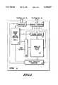
- FIG. 1illustrates, in block diagram form, a data processor 10 in accordance with one embodiment of the present invention
- FIG. 2illustrates, in block diagram form, an EEPROM 22 of FIG. 1 in accordance with one embodiment of the present invention
- FIG. 3illustrates, in block diagram form, charge pump and related circuitry 30 in accordance with one embodiment of the present invention
- FIG. 4illustrates, in schematic diagram form, voltage elevating circuitry 51 of FIG. 3 in accordance with one embodiment of the present invention
- FIG. 5illustrates, in schematic diagram form, clock voltage level shifting circuitry 53 of FIG. 3 in accordance with one embodiment of the present invention.
- FIG. 6illustrates, in graphical form, the relationships between the voltages levels of VSS, VDD, V1, and VOUT, and the maximum and minimum voltage levels of CLOCK1, CLOCK2, and SHIFTED CLOCK signals in accordance with one embodiment of the present invention.
- the present inventionprovides charge pump and related circuitry 30 which can be used to provide a high voltage output (18 volts or more) using a low power supply voltage (below 2 volts). Most prior art charge pumps either do not function properly or cannot generate a sufficiently high output voltage (18 volts or more) below a power supply voltage of approximately 2.0 volts.
- the present inventionutilizes circuitry which extends the operating voltage range for which a charge pump can generate a sufficiently high output voltage. That is, the present invention allows charge pump and related circuitry 30 to operate at power supply voltages below that of prior art charge pumps.
- the present inventionextends the operating voltage range of charge pumps by utilizing voltage elevating circuitry 51 and clock voltage level shifting circuitry 53: (1) to produce stronger clock drives to circuits (e.g. charge pump 57) which control the charge transfer between the stages; and (2) to increase the amount of charge that can be stored on the capacitors in the stages (e.g. in the stages of charge pump 57).
- the present inventioncan continue to produce an output voltage of 18 volts or more using a power supply voltage as low as 1.8 volts (and possibly even lower).
- the present inventionis especially useful in applications that require a high output voltage to be generated using a power supply voltage level as low as 1.8 volts, and possibly lower.
- the inventionmay be especially useful in very low voltage and/or very low power applications such as battery operated applications (e.g. applications involving portable devices such as pagers, lap top computers, global positioning systems, cellular phones, or personal communicators).
- battery operated applicationse.g. applications involving portable devices such as pagers, lap top computers, global positioning systems, cellular phones, or personal communicators.
- the present inventionis especially useful in applications which use one or more batteries in which the device must continue to function even when the battery is supplying as little as 1.8 volts.
- FIGS. 1-6The present invention can be more fully understood with reference to FIGS. 1-6.
- FIG. 1illustrates one embodiment of a data processor 10 that includes a central processing unit (CPU) 12, a timer 14, external bus interface 16, random access memory (RAM) 18, read only memory (ROM) 20, and electrically erasable programmable read only memory (EEPROM) 22, which are all bi-directionally coupled to bus 28.
- Timer 14is coupled external to data processor 10 by way of integrated circuit pins 24.
- External bus interface 16is coupled external to data processor 10 by way of integrated circuit pins 26.
- an external data bus (not shown) and an external address bus (not shown)are coupled to integrated circuit pins 26.
- EEPROM 22may be read and programmed by CPU 12.
- CPU 12uses bus 28 to perform read and/or programming accesses to EEPROM 22.
- data processor 10is a microcontroller formed on a single integrated circuit.
- EEPROM 22may be formed by itself on a single integrated circuit.
- EEPROM 22may be coupled directly to integrated circuit pins 26 in order to receive and provide signals external to EEPROM 22.
- FIG. 2illustrates one embodiment of EEPROM 22 that includes an array of EEPROM cells 36, row decoder 34, column decoder 32, sense amplifier circuitry 38, control circuitry 40, registers 42, and charge pump and related circuitry 30.
- EEPROM 22operates in the same manner as standard prior art EEPROMs.
- charge pump and related circuitry 30the circuitry in EEPROM 22 is standard and is known to one of average skill in the art.
- control circuitry 40 and registers 42are bi-directionally coupled to bus 28.
- Control circuitry 40provides signals to and receives signals from registers 42.
- Control circuitry 40provides signals to and receives signals from charge pump and related circuitry 30.
- Control circuitry 40provides signals to row decoder 34, column decode 32, sense amplifier circuitry 38, and the array of EEPROM cells 36.
- Registers 42provide signals to and receive signals from sense amplifier circuitry 38. Registers 42 also provide signals to and receive signals from charge pump and related circuitry 30.
- Charge pump and related circuitry 30provides signals to row decoder 34, column decoder 32, and sense amplifier circuitry 38.
- Row decoder 34 and column decoder 32provide signals to the array of EEPROM cells 36.
- the array of EEPROM cells 36provides signals to sense amplifier circuitry 38.
- FIG. 3illustrates one embodiment of charge pump and related circuitry 30.
- Charge pump and related circuitry 30includes voltage elevating circuitry 51, clock voltage level shifting circuitry 53, clock separator 55, and charge pump 57.
- charge pump and related circuitry 30receives two clock signals as inputs, namely CLOCK1 and CLOCK2.
- Charge pump and related circuitry 30also receives two power supply voltages, namely VDD and VSS.
- VDDis specified to be in the range of 1.8 volts to 3.2 volts
- VSSis approximately 0 volts (i.e. approximately ground).
- voltage elevating circuitry 51receives a CLOCK2 signal which switches between VSS and VDD, and also receives a power supply voltage VDD. Voltage elevating circuitry 51 provides an elevated, intermediate output voltage, namely V1, at node 59.
- VDDis either an internally or externally supplied operating voltage that has a lower voltage potential than either V1 or VOUT.
- CLOCK2can be either an internally or externally generated signal.
- Clock voltage level shifting circuitry 53receives a CLOCK1 signal which switches between VSS and VDD, and also receives the voltage V1.
- Clock voltage level shifting circuitry 53produces a SHIFTED CLOCK signal 52 which switches between VSS and V1.
- the CLOCK1 signal and the CLOCK2 signalmay be the same signal. In alternate embodiments of the present invention, the CLOCK1 signal and the CLOCK2 signal may be different signals.
- Clock separator circuit 55is a standard, prior art circuit known to one of average skill in the art. However, in the prior art, the clock separator circuit received VDD and CLOCK 1 as inputs, rather than V1 and SHIFTED CLOCK as illustrated in FIG. 3. The present invention thus provides a clock separator circuit 55 with input signals V1 and SHIFTED CLOCK having elevated maximum voltages.
- Clock separator circuit 55produces one or more clock signals which are provided to charge pump 57.
- clock separator circuit 55does not significantly affect the maximum and minimum voltage level of the SHIFTED CLOCK signal.
- CLOCKA signal, CLOCKB signal, CLOCKC signal, and CLOCKD signalhave approximately the same minimum and maximum voltages as the SHIFTED CLOCK signal, namely a minimum voltage level of approximately VSS and a maximum voltage level of approximately V1 (see FIG. 6).
- clock separator circuit 55is a standard non-overlapping, 2-phase clock separator. In an alternate embodiment of the present invention, clock separator 55 does not alter the SHIFTED CLOCK signal, but merely passes the SHIFTED CLOCK signal through to charge pump 57.
- Charge pump circuit 57is a standard, prior art charge pump known to one of average skill in the art.
- charge pump 57uses a series of "bucket-brigade" stages to build up the output voltage VOUT.
- the charge pump circuitreceived one or more clocks which did not have elevated maximum voltages.
- charge pump 57receives one or more clocks, namely CLOCKA, CLOCKB, CLOCKC, and CLOCKD, which do have elevated maximum voltages.
- the present inventionthus provides a charge pump circuit 57 with one or more input clock signals having elevated maximum voltages.
- each individual stage of charge pump circuit 57includes a circuit that controls charge transfer (not shown) and a capacitor (not shown) to store the transferred charge.
- Charge pump 57receives power supply voltage VDD and one or more clock signals provided by clock separator 55.
- Charge pump 57provides an output voltage VOUT that has a higher voltage potential than either VDD or V1.
- the output voltage VOUTmay be used for a variety of applications which require an elevated voltage above that of the power supply voltage VDD. Note that for the illustrated embodiment of the present invention, a power supply voltage VDD as low as 1.8 volts may be used to provide an output voltage VOUT as high as 18 volts.
- FIG. 4illustrates one embodiment of the voltage elevating circuitry 51 of FIG. 3.
- voltage elevating circuitry 51includes a circuit 61, a circuit 63, a circuit 65, a circuit 67, and a circuit 69 as illustrated in FIG. 4.
- inverting logic gate 130 and inverting logic gate 132each have an input coupled to receive a CLOCK2 signal.
- the output of inverting logic gate 130is coupled to an input of inverting logic gate 131.
- the output of inverting logic gate 132is coupled to a data input of transmission logic gate 133.
- a first control input of transmission logic gate 133is coupled to a positive power supply voltage terminal for receiving a positive power supply voltage labeled VDD.
- transmission logic gate 133is in a conducting state when the first power supply voltage VDD is being applied.
- N-channel MOSFET transistors 101, 103, 105, and 107each have a first current electrode coupled to the positive power supply voltage terminal for receiving the positive power supply voltage VDD.
- Transistor 101has a control electrode coupled to the positive power supply voltage; likewise transistor 107 has a control electrode coupled to the positive power supply voltage.
- a capacitive element 121has a first electrode coupled to a second current electrode of transistor 101, to a second current electrode of transistor 103, to a control electrode of transistor 105, and to a node 108.
- the capacitive element 121has a second electrode coupled to node 102.
- Node 102is also coupled to the output of inverting logic gate 131.
- a capacitive element 122has a first electrode coupled to a second current electrode of transistor 105, to a second current electrode of transistor 107, to a control electrode of transistor 103, and to a node 106.
- the capacitive element 122has a second electrode coupled to node 104.
- Node 104is also coupled to the data output of transmission logic gate 133.
- N-channel MOSFET transistor 109has a first current electrode coupled to node 106.
- N-channel MOSFET transistor 111has a first current electrode coupled to node 108.
- a capacitive element 123has a first electrode coupled to a second current electrode of transistor 109, to a control electrode of transistor 111, and to a node 112.
- the capacitive element 123has a second electrode coupled to node 102.
- a capacitive element 124has a first electrode coupled to a second current electrode of transistor 111, to a control electrode of transistor 109, and to a node 110.
- the capacitive element 124has a second electrode coupled to node 104.
- N-channel MOSFET transistor 113has a first current electrode and a control electrode coupled to node 112.
- a capacitive element 125has a first electrode coupled to a second current electrode of transistor 113 and to a node 59.
- the capacitive element 125has a second electrode coupled to a second power supply voltage terminal for receiving a power supply voltage labeled VSS.
- VSSis an approximately ground potential.
- Voltage elevating circuitry 51provides a voltage V1 at node 59.
- the voltage V1is at a higher potential than the power supply voltage VDD.
- voltage elevating circuitry 51functions as a secondary charge pump circuit that is more suitable for generating an elevated, intermediate voltage V1, rather than for providing a higher potential final output voltage such as VOUT.
- One potential problem with using voltage elevating circuitry 51 as a primary charge pump, such as charge pump 57 in FIG. 3,is that the capacitors 121-125 required to handle a large load coupled to node 59 may require a significant amount of semiconductor area on an integrated circuit. For example, under some loading conditions, each capacitor 121-125 may be 10 picofarads or more.
- the voltage elevating circuitry 51may be used to provide the final output voltage VOUT in an alternate embodiment of the present invention, this alternate embodiment may require more semiconductor area than a typical prior art charge pump.
- VGSxxxrefers to the gate-to-source voltage of transistor xxx.
- the input clock signalnamely CLOCK2
- CLOCK2is separated by circuit 69 into non-overlapping, non-inverting and inverting signals provided to circuits 61 and 63 at nodes 102 and 104.
- Circuits 61 and 63receive the non-inverting clock signal at node 102, and the inverting clock signal at node 104.
- Circuit 61acts as a first stage of voltage elevating circuitry 51. Initially, when CLOCK2 is at its minimum voltage level, namely VSS, node 102 is also at voltage VSS. As a result, capacitive element 121 is charged to (VDD-VGS101) since transistor 101 behaves as a diode.
- the voltage at node 108is [VDD+(VDD-VGS101)]. As the voltage at node 108 is elevated, positive feedback through transistor 105 pulls node 106 up to VDD. At this point, capacitor 122 is charged up to VDD, rather than to (VDD-VGS107).
- the voltage at node 106is elevated to (2*VDD) and positive feedback through transistor 103 pulls node 108 up to VDD, charging capacitive element 121 to VDD.
- circuit 61uses positive feedback to provide higher charging efficiency, thus eliminating the voltage drop associated with transistors such as transistor 101 and transistor 107.
- the second stageuses the voltage of (2*VDD) at node 106 to accomplish the task of elevating the voltage at node 112 to the voltage of (3*VDD).
- node 106reaches the voltage of (2*VDD) as the CLOCK2 signal transitions to VSS, node 124 goes high to VDD and node 110 is at VDD. This causes transistor 109 to conduct and node 112 to elevate to the voltage (2*VDD).
- node 112is elevated to the voltage (3*VDD), which is VDD above the output of the first stage circuit 61.
- circuit 61is the same as circuit 63 with the addition of transistors 101 and 107.
- Transistor 101is used to precharge capacitive element 121 to a voltage of (VDD-VGS101), and transistor 107 is used to precharge capacitive element 122 to a voltage of (VDD-VGS107).
- circuit 61as the first charge pump stage
- circuit 63as the second charge pump stage
- alternate embodiments of the present inventionmay use one or more charge pump stages.
- a third charge pump stageif a third charge pump stage is desired, a duplicate of circuit 63 may be coupled to existing circuit 63 in the same manner that existing circuit 63 is coupled to circuit 61.
- Each charge pump stagei.e. each circuit 63, can be used to elevate the voltage at node 112 by an additional VDD.
- a total of "N" stagesi.e. circuits 63
- were coupled to the output of the first stagei.e.
- the voltage at node 112would be elevated to approximately [(2*VDD)+(N*VDD)]. Note that the voltage V1 may actually be less than [(2*VDD)+(N*VDD)], depending upon the load coupled to node 59.
- Circuit 65 and circuit 67convert the output voltage of the final stage, namely V1, into a DC voltage (i.e. an output voltage that maintains an approximately constant voltage level).
- Circuit 65behaves as a diode by preventing charge from being conducted from node 59 back to node 112.
- Circuit 67stores charge and helps to maintain the voltage V1 at an approximately constant voltage. Note that there is a voltage drop across the transistor 113.
- the net output voltage V1 of voltage elevating circuitry 51is the output voltage from the final stage, e.g. (3*VDD) at node 112, minus the voltage drop across the circuit 65.
- one or more diodes or transistorscan be used for clamping V1 if it is necessary to prevent the intermediate output voltage V1 from exceeding a predetermined voltage level.
- FIG. 5illustrates one embodiment of the clock voltage level shifter circuit 53 of FIG. 3.
- clock voltage level shifter circuit 53includes a circuit 240 and a buffer circuit 230-233 as illustrated in FIG. 4.
- inverting logic gate 234has an input coupled to receive a CLOCK1 signal.
- P-channel MOSFET transistors 221 and 223each have a first current electrode coupled to node 59 for receiving the voltage V1.
- N-channel MOSFET transistor 225has a first current electrode coupled to a second current electrode of transistor 221 and coupled to a control electrode of transistor 223.
- Transistor 225has a second current electrode which is coupled to the second power supply voltage terminal for receiving a power supply voltage labeled VSS.
- Transistor 225has a control electrode for receiving the CLOCK1 signal.
- N-channel MOSFET transistor 227has a first current electrode coupled to a second current electrode of transistor 223 and coupled to a control electrode of transistor 221.
- Transistor 227has a second current electrode which is coupled to the second power supply voltage terminal for receiving a power supply voltage VSS.
- Transistor 227has a control electrode coupled to the output of inverting logic gate 234 for receiving the inverted CLOCK1 signal.
- Buffer circuit 230-233is optional. Buffer circuit 230-233 may be used to increase the drive capability of the SHIFTED CLOCK signal provided at conductor 52. The greater the drive capability of the SHIFTED CLOCK signal, the larger the load which can be driven by the SHIFTED CLOCK signal.
- the embodiment of the present invention illustrated in FIG. 5uses a plurality of series coupled inverting logic gates, namely inverting logic gates 230-233, alternate embodiments of the present invention may use more inverting logic gates, fewer inverting logic gates, or different inverting logic gates.
- Clock voltage level shifting circuitry 53receives the CLOCK1 signal and provides a SHIFTED CLOCK signal which is the same as the CLOCK1 signal, except that the maximum voltage level of the CLOCK1 signal is VDD, and the maximum voltage level of the SHIFTED CLOCK signal is V1.
- clock voltage level shifting circuitry 53effectively elevates the maximum voltage of CLOCK1 from VDD to the intermediate voltage level V1.
- transistor 225is conducting while transistor 227 is non-conducting.
- node 222is at the voltage VSS, which causes transistor 223 to conduct.
- Node 220is held to the voltage level at node 59, namely V1, which is coupled to the output node 59 of the voltage elevating circuitry 51.
- transistor 221is non-conducting.
- FIG. 6illustrates the relationships between the voltages levels of VSS, VDD, V1, and VOUT.
- FIG. 6also illustrates the maximum and minimum voltage levels of CLOCK1, CLOCK2, and SHIFTED CLOCK.
- the present inventionprovides charge pump and related circuitry 30 which can be used to provide a high voltage output (18 volts or more) using a low power supply voltage (below 2 volts).
- the present inventionextends the operating voltage range of charge pumps by utilizing voltage elevating circuitry 51 and clock voltage level shifting circuitry 53: (1) to produce stronger clock drives to circuits (e.g. clock separator 55) which control the charge transfer between the stages; and (2) to increase the amount of charge that can be stored on the capacitors in the stages (e.g. in the stages of charge pump 57).
- the present inventioncan continue to produce an output voltage of 18 volts or more using a power supply voltage as low as 1.8 volts (and possibly even lower).
Landscapes
- Engineering & Computer Science (AREA)
- Power Engineering (AREA)
- Microelectronics & Electronic Packaging (AREA)
- Physics & Mathematics (AREA)
- Nonlinear Science (AREA)
- Electromagnetism (AREA)
- General Physics & Mathematics (AREA)
- Radar, Positioning & Navigation (AREA)
- Automation & Control Theory (AREA)
- Dc-Dc Converters (AREA)
Abstract
Description
Claims (20)
Priority Applications (1)
| Application Number | Priority Date | Filing Date | Title |
|---|---|---|---|
| US08/144,361US5394027A (en) | 1993-11-01 | 1993-11-01 | High voltage charge pump and related circuitry |
Applications Claiming Priority (1)
| Application Number | Priority Date | Filing Date | Title |
|---|---|---|---|
| US08/144,361US5394027A (en) | 1993-11-01 | 1993-11-01 | High voltage charge pump and related circuitry |
Publications (1)
| Publication Number | Publication Date |
|---|---|
| US5394027Atrue US5394027A (en) | 1995-02-28 |
Family
ID=22508245
Family Applications (1)
| Application Number | Title | Priority Date | Filing Date |
|---|---|---|---|
| US08/144,361Expired - LifetimeUS5394027A (en) | 1993-11-01 | 1993-11-01 | High voltage charge pump and related circuitry |
Country Status (1)
| Country | Link |
|---|---|
| US (1) | US5394027A (en) |
Cited By (19)
| Publication number | Priority date | Publication date | Assignee | Title |
|---|---|---|---|---|
| WO1995026071A1 (en)* | 1994-03-23 | 1995-09-28 | Intel Corporation | Method and apparatus for providing an ultra low power regulated negative charge pump |
| US5499183A (en)* | 1993-11-30 | 1996-03-12 | Nec Corporation | Constant voltage generating circuit having step-up circuit |
| US5513091A (en)* | 1994-03-29 | 1996-04-30 | Kabushiki Kaisha Toshiba | Voltage transforming circuit |
| US5535160A (en)* | 1993-07-05 | 1996-07-09 | Mitsubishi Denki Kabushiki Kaisha | Semiconductor integrated circuit |
| WO1996028877A1 (en)* | 1995-03-09 | 1996-09-19 | Macronix International Co., Ltd. | Regulated reference voltage circuit for flash memory device and other integrated circuit applications |
| US5621685A (en)* | 1994-10-17 | 1997-04-15 | Sandisk Corporation | Programmable power generation circuit for flash EEPROM memory systems |
| US5666070A (en)* | 1995-05-10 | 1997-09-09 | Micron Technology, Inc. | Low power, high speed level shifter |
| EP0822477A3 (en)* | 1996-07-29 | 1998-04-01 | Townsend and Townsend and Crew LLP | Charge pump for a semiconductor substrate |
| US5973956A (en)* | 1995-07-31 | 1999-10-26 | Information Storage Devices, Inc. | Non-volatile electrically alterable semiconductor memory for analog and digital storage |
| US6150879A (en)* | 1997-09-22 | 2000-11-21 | Nec Corporation | Semiconductor apparatus for use in low voltage power supply |
| US6166585A (en)* | 1998-08-31 | 2000-12-26 | Conexant Systems, Inc. | Methods and apparatus for a high efficiency charge pump that includes a MOSFET capacitor operating in an accumulation region |
| WO2001017097A1 (en)* | 1999-08-31 | 2001-03-08 | Intel Corporation | Split clock buffers for a negative charge pump |
| US6366519B1 (en) | 1995-03-09 | 2002-04-02 | Macronix International Co., Ltd. | Regulated reference voltage circuit for flash memory device and other integrated circuit applications |
| US6577535B2 (en) | 2001-02-16 | 2003-06-10 | Sandisk Corporation | Method and system for distributed power generation in multi-chip memory systems |
| US20050195017A1 (en)* | 2004-03-03 | 2005-09-08 | Tien-Tzu Chen | High efficiency charge pump with prevention from reverse current |
| WO2006102927A1 (en)* | 2005-04-01 | 2006-10-05 | Freescale Semiconductor, Inc. | Charge pump and control scheme |
| US20090296439A1 (en)* | 2008-05-29 | 2009-12-03 | Weiwei Qi | Multi output voltage regulation of a synchronous generator in a power system |
| US20100001696A1 (en)* | 2008-07-01 | 2010-01-07 | Hwang Charlie C | System to improve a multistage charge pump and associated methods |
| US20150042398A1 (en)* | 2013-08-08 | 2015-02-12 | Micron Technology, Inc. | Charge pump including supply voltage-based control signal level |
Citations (11)
| Publication number | Priority date | Publication date | Assignee | Title |
|---|---|---|---|---|
| US4326134A (en)* | 1979-08-31 | 1982-04-20 | Xicor, Inc. | Integrated rise-time regulated voltage generator systems |
| US4486670A (en)* | 1982-01-19 | 1984-12-04 | Intersil, Inc. | Monolithic CMOS low power digital level shifter |
| US4710647A (en)* | 1986-02-18 | 1987-12-01 | Intel Corporation | Substrate bias generator including multivibrator having frequency independent of supply voltage |
| US4792705A (en)* | 1986-03-14 | 1988-12-20 | Western Digital Corporation | Fast switching charge pump |
| US5081371A (en)* | 1990-11-07 | 1992-01-14 | U.S. Philips Corp. | Integrated charge pump circuit with back bias voltage reduction |
| US5111375A (en)* | 1990-12-20 | 1992-05-05 | Texas Instruments Incorporated | Charge pump |
| US5126590A (en)* | 1991-06-17 | 1992-06-30 | Micron Technology, Inc. | High efficiency charge pump |
| US5134317A (en)* | 1990-05-31 | 1992-07-28 | Sharp Kabushiki Kaisha | Booster circuit for a semiconductor memory device |
| US5138190A (en)* | 1988-09-13 | 1992-08-11 | Kabushiki Kaisha Toshiba | Charge pump circuit |
| US5153855A (en)* | 1989-07-14 | 1992-10-06 | Seiko Instruments Inc. | Semiconductor nonvolatile memory device integrated with booster |
| US5168174A (en)* | 1991-07-12 | 1992-12-01 | Texas Instruments Incorporated | Negative-voltage charge pump with feedback control |
- 1993
- 1993-11-01USUS08/144,361patent/US5394027A/ennot_activeExpired - Lifetime
Patent Citations (11)
| Publication number | Priority date | Publication date | Assignee | Title |
|---|---|---|---|---|
| US4326134A (en)* | 1979-08-31 | 1982-04-20 | Xicor, Inc. | Integrated rise-time regulated voltage generator systems |
| US4486670A (en)* | 1982-01-19 | 1984-12-04 | Intersil, Inc. | Monolithic CMOS low power digital level shifter |
| US4710647A (en)* | 1986-02-18 | 1987-12-01 | Intel Corporation | Substrate bias generator including multivibrator having frequency independent of supply voltage |
| US4792705A (en)* | 1986-03-14 | 1988-12-20 | Western Digital Corporation | Fast switching charge pump |
| US5138190A (en)* | 1988-09-13 | 1992-08-11 | Kabushiki Kaisha Toshiba | Charge pump circuit |
| US5153855A (en)* | 1989-07-14 | 1992-10-06 | Seiko Instruments Inc. | Semiconductor nonvolatile memory device integrated with booster |
| US5134317A (en)* | 1990-05-31 | 1992-07-28 | Sharp Kabushiki Kaisha | Booster circuit for a semiconductor memory device |
| US5081371A (en)* | 1990-11-07 | 1992-01-14 | U.S. Philips Corp. | Integrated charge pump circuit with back bias voltage reduction |
| US5111375A (en)* | 1990-12-20 | 1992-05-05 | Texas Instruments Incorporated | Charge pump |
| US5126590A (en)* | 1991-06-17 | 1992-06-30 | Micron Technology, Inc. | High efficiency charge pump |
| US5168174A (en)* | 1991-07-12 | 1992-12-01 | Texas Instruments Incorporated | Negative-voltage charge pump with feedback control |
Non-Patent Citations (2)
| Title |
|---|
| Duane Oto et al., "High-Voltage Regulation and Process Considerations for High-Density 5V-Only E2PROM's", IEEE Journal of Solid-State Circuits, vol. SC-18, No. 5, Oct. 1983, pp. 532-538. |
| Duane Oto et al., High Voltage Regulation and Process Considerations for High Density 5V Only E2PROM s , IEEE Journal of Solid State Circuits, vol. SC 18, No. 5, Oct. 1983, pp. 532 538.* |
Cited By (33)
| Publication number | Priority date | Publication date | Assignee | Title |
|---|---|---|---|---|
| US5535160A (en)* | 1993-07-05 | 1996-07-09 | Mitsubishi Denki Kabushiki Kaisha | Semiconductor integrated circuit |
| US5499183A (en)* | 1993-11-30 | 1996-03-12 | Nec Corporation | Constant voltage generating circuit having step-up circuit |
| WO1995026071A1 (en)* | 1994-03-23 | 1995-09-28 | Intel Corporation | Method and apparatus for providing an ultra low power regulated negative charge pump |
| US5532915A (en)* | 1994-03-23 | 1996-07-02 | Intel Corporation | Method and apparatus for providing an ultra low power regulated negative charge pump |
| US5513091A (en)* | 1994-03-29 | 1996-04-30 | Kabushiki Kaisha Toshiba | Voltage transforming circuit |
| US5621685A (en)* | 1994-10-17 | 1997-04-15 | Sandisk Corporation | Programmable power generation circuit for flash EEPROM memory systems |
| US5693570A (en)* | 1994-10-17 | 1997-12-02 | Sandisk Corporation | Process for manufacturing a programmable power generation circuit for flash EEPROM memory systems |
| WO1996028877A1 (en)* | 1995-03-09 | 1996-09-19 | Macronix International Co., Ltd. | Regulated reference voltage circuit for flash memory device and other integrated circuit applications |
| US6366519B1 (en) | 1995-03-09 | 2002-04-02 | Macronix International Co., Ltd. | Regulated reference voltage circuit for flash memory device and other integrated circuit applications |
| US5666070A (en)* | 1995-05-10 | 1997-09-09 | Micron Technology, Inc. | Low power, high speed level shifter |
| US5973956A (en)* | 1995-07-31 | 1999-10-26 | Information Storage Devices, Inc. | Non-volatile electrically alterable semiconductor memory for analog and digital storage |
| US6323721B1 (en) | 1996-07-26 | 2001-11-27 | Townsend And Townsend And Crew Llp | Substrate voltage detector |
| US6323722B1 (en) | 1996-07-29 | 2001-11-27 | Townsend And Townsend And Crew Llp | Apparatus for translating a voltage |
| US6137335A (en)* | 1996-07-29 | 2000-10-24 | Townsend And Townsend And Crew Llp | Oscillator receiving variable supply voltage depending on substrate voltage detection |
| US6064250A (en)* | 1996-07-29 | 2000-05-16 | Townsend And Townsend And Crew Llp | Various embodiments for a low power adaptive charge pump circuit |
| US6326839B2 (en) | 1996-07-29 | 2001-12-04 | Townsend And Townsend And Crew Llp | Apparatus for translating a voltage |
| EP0822477A3 (en)* | 1996-07-29 | 1998-04-01 | Townsend and Townsend and Crew LLP | Charge pump for a semiconductor substrate |
| US6150879A (en)* | 1997-09-22 | 2000-11-21 | Nec Corporation | Semiconductor apparatus for use in low voltage power supply |
| CN1081406C (en)* | 1997-09-22 | 2002-03-20 | 日本电气株式会社 | Semiconductor apparatus for use in low voltage power supply |
| US6166585A (en)* | 1998-08-31 | 2000-12-26 | Conexant Systems, Inc. | Methods and apparatus for a high efficiency charge pump that includes a MOSFET capacitor operating in an accumulation region |
| WO2001017097A1 (en)* | 1999-08-31 | 2001-03-08 | Intel Corporation | Split clock buffers for a negative charge pump |
| US6359947B1 (en) | 1999-08-31 | 2002-03-19 | Intel Corporation | Split clock buffers for a negative charge pump |
| US6577535B2 (en) | 2001-02-16 | 2003-06-10 | Sandisk Corporation | Method and system for distributed power generation in multi-chip memory systems |
| US20050195017A1 (en)* | 2004-03-03 | 2005-09-08 | Tien-Tzu Chen | High efficiency charge pump with prevention from reverse current |
| US6995603B2 (en) | 2004-03-03 | 2006-02-07 | Aimtron Technology Corp. | High efficiency charge pump with prevention from reverse current |
| WO2006102927A1 (en)* | 2005-04-01 | 2006-10-05 | Freescale Semiconductor, Inc. | Charge pump and control scheme |
| US20100308890A1 (en)* | 2005-04-01 | 2010-12-09 | Freescale Semiconductor, Inc. | Charge pump and control scheme |
| US7999601B2 (en) | 2005-04-01 | 2011-08-16 | Freescale Semiconductor, Inc. | Charge pump and control scheme |
| US20090296439A1 (en)* | 2008-05-29 | 2009-12-03 | Weiwei Qi | Multi output voltage regulation of a synchronous generator in a power system |
| US20100001696A1 (en)* | 2008-07-01 | 2010-01-07 | Hwang Charlie C | System to improve a multistage charge pump and associated methods |
| US8258758B2 (en)* | 2008-07-01 | 2012-09-04 | International Business Machines Corporation | System to improve a multistage charge pump and associated methods |
| US20150042398A1 (en)* | 2013-08-08 | 2015-02-12 | Micron Technology, Inc. | Charge pump including supply voltage-based control signal level |
| US9246382B2 (en)* | 2013-08-08 | 2016-01-26 | Micron Technology, Inc. | Charge pump including supply voltage-based control signal level |
Similar Documents
| Publication | Publication Date | Title |
|---|---|---|
| US5394027A (en) | High voltage charge pump and related circuitry | |
| US5524266A (en) | System having multiple phase boosted charge pump with a plurality of stages | |
| US5841703A (en) | Method and apparatus for removal of VT drop in the output diode of charge pumps | |
| US5414669A (en) | Method and apparatus for programming and erasing flash EEPROM memory arrays utilizing a charge pump circuit | |
| US6188293B1 (en) | Low power oscillation circuit and non-volatile semiconductor memory having ring oscillator | |
| US5905402A (en) | Voltage pump circuit having an independent well-bias voltage | |
| US6614699B2 (en) | Booster circuit for raising voltage by sequentially transferring charges from input terminals of booster units to output terminals thereof in response to clock signals having different phases | |
| US5365121A (en) | Charge pump with controlled ramp rate | |
| CA2185333C (en) | Method and apparatus for providing an ultra low power regulated negative charge pump | |
| KR100287545B1 (en) | Nonvolatile Semiconductor Memory Devices | |
| US6160440A (en) | Scaleable charge pump for use with a low voltage power supply | |
| EP0376065B1 (en) | Semiconductor memory integrated circuit | |
| WO2020081139A1 (en) | Improved charge pump for use in non-volatile flash memory devices | |
| US6359947B1 (en) | Split clock buffers for a negative charge pump | |
| KR20190103008A (en) | Level shifter and semiconductor device | |
| US6385099B1 (en) | Reducing level shifter standby power consumption | |
| US6028780A (en) | Two-phase clock charge pump with power regulation | |
| EP1278202B1 (en) | Nonvolatile semiconductor storage device | |
| US6191642B1 (en) | Charge pump circuit | |
| US20040000945A1 (en) | Pumping circuit | |
| US6373780B1 (en) | Single supply voltage nonvolatile memory device with row decoding | |
| US4831589A (en) | EEPROM programming switch operable at low VCC | |
| US6430093B1 (en) | CMOS boosting circuit utilizing ferroelectric capacitors | |
| JPH1069796A (en) | Semiconductor integrated circuit with high-speed test function |
Legal Events
| Date | Code | Title | Description |
|---|---|---|---|
| AS | Assignment | Owner name:MOTOROLA, INC., ILLINOIS Free format text:ASSIGNMENT OF ASSIGNORS INTEREST;ASSIGNOR:PARK, DAVID KIESUNG;REEL/FRAME:006765/0743 Effective date:19931027 | |
| STCF | Information on status: patent grant | Free format text:PATENTED CASE | |
| FPAY | Fee payment | Year of fee payment:4 | |
| FPAY | Fee payment | Year of fee payment:8 | |
| AS | Assignment | Owner name:FREESCALE SEMICONDUCTOR, INC., TEXAS Free format text:ASSIGNMENT OF ASSIGNORS INTEREST;ASSIGNOR:MOTOROLA, INC.;REEL/FRAME:015698/0657 Effective date:20040404 Owner name:FREESCALE SEMICONDUCTOR, INC.,TEXAS Free format text:ASSIGNMENT OF ASSIGNORS INTEREST;ASSIGNOR:MOTOROLA, INC.;REEL/FRAME:015698/0657 Effective date:20040404 | |
| FPAY | Fee payment | Year of fee payment:12 | |
| AS | Assignment | Owner name:CITIBANK, N.A. AS COLLATERAL AGENT, NEW YORK Free format text:SECURITY AGREEMENT;ASSIGNORS:FREESCALE SEMICONDUCTOR, INC.;FREESCALE ACQUISITION CORPORATION;FREESCALE ACQUISITION HOLDINGS CORP.;AND OTHERS;REEL/FRAME:018855/0129 Effective date:20061201 Owner name:CITIBANK, N.A. AS COLLATERAL AGENT,NEW YORK Free format text:SECURITY AGREEMENT;ASSIGNORS:FREESCALE SEMICONDUCTOR, INC.;FREESCALE ACQUISITION CORPORATION;FREESCALE ACQUISITION HOLDINGS CORP.;AND OTHERS;REEL/FRAME:018855/0129 Effective date:20061201 | |
| AS | Assignment | Owner name:CITIBANK, N.A., AS COLLATERAL AGENT,NEW YORK Free format text:SECURITY AGREEMENT;ASSIGNOR:FREESCALE SEMICONDUCTOR, INC.;REEL/FRAME:024397/0001 Effective date:20100413 Owner name:CITIBANK, N.A., AS COLLATERAL AGENT, NEW YORK Free format text:SECURITY AGREEMENT;ASSIGNOR:FREESCALE SEMICONDUCTOR, INC.;REEL/FRAME:024397/0001 Effective date:20100413 | |
| AS | Assignment | Owner name:CITIBANK, N.A., AS NOTES COLLATERAL AGENT, NEW YORK Free format text:SECURITY AGREEMENT;ASSIGNOR:FREESCALE SEMICONDUCTOR, INC.;REEL/FRAME:030633/0424 Effective date:20130521 Owner name:CITIBANK, N.A., AS NOTES COLLATERAL AGENT, NEW YOR Free format text:SECURITY AGREEMENT;ASSIGNOR:FREESCALE SEMICONDUCTOR, INC.;REEL/FRAME:030633/0424 Effective date:20130521 | |
| AS | Assignment | Owner name:CITIBANK, N.A., AS NOTES COLLATERAL AGENT, NEW YORK Free format text:SECURITY AGREEMENT;ASSIGNOR:FREESCALE SEMICONDUCTOR, INC.;REEL/FRAME:031591/0266 Effective date:20131101 Owner name:CITIBANK, N.A., AS NOTES COLLATERAL AGENT, NEW YOR Free format text:SECURITY AGREEMENT;ASSIGNOR:FREESCALE SEMICONDUCTOR, INC.;REEL/FRAME:031591/0266 Effective date:20131101 | |
| AS | Assignment | Owner name:FREESCALE SEMICONDUCTOR, INC., TEXAS Free format text:PATENT RELEASE;ASSIGNOR:CITIBANK, N.A., AS COLLATERAL AGENT;REEL/FRAME:037356/0553 Effective date:20151207 Owner name:FREESCALE SEMICONDUCTOR, INC., TEXAS Free format text:PATENT RELEASE;ASSIGNOR:CITIBANK, N.A., AS COLLATERAL AGENT;REEL/FRAME:037356/0143 Effective date:20151207 Owner name:FREESCALE SEMICONDUCTOR, INC., TEXAS Free format text:PATENT RELEASE;ASSIGNOR:CITIBANK, N.A., AS COLLATERAL AGENT;REEL/FRAME:037354/0225 Effective date:20151207 | |
| AS | Assignment | Owner name:MORGAN STANLEY SENIOR FUNDING, INC., MARYLAND Free format text:ASSIGNMENT AND ASSUMPTION OF SECURITY INTEREST IN PATENTS;ASSIGNOR:CITIBANK, N.A.;REEL/FRAME:037486/0517 Effective date:20151207 | |
| AS | Assignment | Owner name:MORGAN STANLEY SENIOR FUNDING, INC., MARYLAND Free format text:ASSIGNMENT AND ASSUMPTION OF SECURITY INTEREST IN PATENTS;ASSIGNOR:CITIBANK, N.A.;REEL/FRAME:037518/0292 Effective date:20151207 | |
| AS | Assignment | Owner name:NXP, B.V., F/K/A FREESCALE SEMICONDUCTOR, INC., NETHERLANDS Free format text:RELEASE BY SECURED PARTY;ASSIGNOR:MORGAN STANLEY SENIOR FUNDING, INC.;REEL/FRAME:040925/0001 Effective date:20160912 Owner name:NXP, B.V., F/K/A FREESCALE SEMICONDUCTOR, INC., NE Free format text:RELEASE BY SECURED PARTY;ASSIGNOR:MORGAN STANLEY SENIOR FUNDING, INC.;REEL/FRAME:040925/0001 Effective date:20160912 | |
| AS | Assignment | Owner name:NXP B.V., NETHERLANDS Free format text:RELEASE BY SECURED PARTY;ASSIGNOR:MORGAN STANLEY SENIOR FUNDING, INC.;REEL/FRAME:040928/0001 Effective date:20160622 | |
| AS | Assignment | Owner name:MORGAN STANLEY SENIOR FUNDING, INC., MARYLAND Free format text:CORRECTIVE ASSIGNMENT TO CORRECT THE REMOVE PATENTS 8108266 AND 8062324 AND REPLACE THEM WITH 6108266 AND 8060324 PREVIOUSLY RECORDED ON REEL 037518 FRAME 0292. ASSIGNOR(S) HEREBY CONFIRMS THE ASSIGNMENT AND ASSUMPTION OF SECURITY INTEREST IN PATENTS;ASSIGNOR:CITIBANK, N.A.;REEL/FRAME:041703/0536 Effective date:20151207 | |
| AS | Assignment | Owner name:SHENZHEN XINGUODU TECHNOLOGY CO., LTD., CHINA Free format text:CORRECTIVE ASSIGNMENT TO CORRECT THE TO CORRECT THE APPLICATION NO. FROM 13,883,290 TO 13,833,290 PREVIOUSLY RECORDED ON REEL 041703 FRAME 0536. ASSIGNOR(S) HEREBY CONFIRMS THE THE ASSIGNMENT AND ASSUMPTION OF SECURITYINTEREST IN PATENTS.;ASSIGNOR:MORGAN STANLEY SENIOR FUNDING, INC.;REEL/FRAME:048734/0001 Effective date:20190217 | |
| AS | Assignment | Owner name:MORGAN STANLEY SENIOR FUNDING, INC., MARYLAND Free format text:CORRECTIVE ASSIGNMENT TO CORRECT THE REMOVE APPLICATION11759915 AND REPLACE IT WITH APPLICATION 11759935 PREVIOUSLY RECORDED ON REEL 037486 FRAME 0517. ASSIGNOR(S) HEREBY CONFIRMS THE ASSIGNMENT AND ASSUMPTION OF SECURITYINTEREST IN PATENTS;ASSIGNOR:CITIBANK, N.A.;REEL/FRAME:053547/0421 Effective date:20151207 | |
| AS | Assignment | Owner name:NXP B.V., NETHERLANDS Free format text:CORRECTIVE ASSIGNMENT TO CORRECT THE REMOVEAPPLICATION 11759915 AND REPLACE IT WITH APPLICATION11759935 PREVIOUSLY RECORDED ON REEL 040928 FRAME 0001. ASSIGNOR(S) HEREBY CONFIRMS THE RELEASE OF SECURITYINTEREST;ASSIGNOR:MORGAN STANLEY SENIOR FUNDING, INC.;REEL/FRAME:052915/0001 Effective date:20160622 | |
| AS | Assignment | Owner name:NXP, B.V. F/K/A FREESCALE SEMICONDUCTOR, INC., NETHERLANDS Free format text:CORRECTIVE ASSIGNMENT TO CORRECT THE REMOVEAPPLICATION 11759915 AND REPLACE IT WITH APPLICATION11759935 PREVIOUSLY RECORDED ON REEL 040925 FRAME 0001. ASSIGNOR(S) HEREBY CONFIRMS THE RELEASE OF SECURITYINTEREST;ASSIGNOR:MORGAN STANLEY SENIOR FUNDING, INC.;REEL/FRAME:052917/0001 Effective date:20160912 |