US5393647A - Method of making superhard tips for micro-probe microscopy and field emission - Google Patents
Method of making superhard tips for micro-probe microscopy and field emissionDownload PDFInfo
- Publication number
- US5393647A US5393647AUS08/092,780US9278093AUS5393647AUS 5393647 AUS5393647 AUS 5393647AUS 9278093 AUS9278093 AUS 9278093AUS 5393647 AUS5393647 AUS 5393647A
- Authority
- US
- United States
- Prior art keywords
- tip
- converted
- silicon
- compound
- tips
- Prior art date
- Legal status (The legal status is an assumption and is not a legal conclusion. Google has not performed a legal analysis and makes no representation as to the accuracy of the status listed.)
- Expired - Fee Related
Links
- 239000000523sampleSubstances0.000titleclaimsabstractdescription12
- 238000000386microscopyMethods0.000titleclaimsdescription8
- 238000004519manufacturing processMethods0.000titleclaimsdescription5
- 239000000463materialSubstances0.000claimsabstractdescription32
- 229910052710siliconInorganic materials0.000claimsabstractdescription26
- 239000010703siliconSubstances0.000claimsabstractdescription25
- QGZKDVFQNNGYKY-UHFFFAOYSA-NAmmoniaChemical compoundNQGZKDVFQNNGYKY-UHFFFAOYSA-N0.000claimsabstractdescription18
- VNWKTOKETHGBQD-UHFFFAOYSA-NmethaneChemical compoundCVNWKTOKETHGBQD-UHFFFAOYSA-N0.000claimsabstractdescription18
- ATUOYWHBWRKTHZ-UHFFFAOYSA-NPropaneChemical compoundCCCATUOYWHBWRKTHZ-UHFFFAOYSA-N0.000claimsabstractdescription10
- 229910021529ammoniaInorganic materials0.000claimsabstractdescription8
- HSFWRNGVRCDJHI-UHFFFAOYSA-Nalpha-acetyleneNatural productsC#CHSFWRNGVRCDJHI-UHFFFAOYSA-N0.000claimsabstractdescription7
- 125000002534ethynyl groupChemical group[H]C#C*0.000claimsabstractdescription7
- 239000001294propaneSubstances0.000claimsabstractdescription5
- 239000000126substanceSubstances0.000claimsabstractdescription4
- 238000000034methodMethods0.000claimsdescription41
- XUIMIQQOPSSXEZ-UHFFFAOYSA-NSiliconChemical compound[Si]XUIMIQQOPSSXEZ-UHFFFAOYSA-N0.000claimsdescription24
- 229910010271silicon carbideInorganic materials0.000claimsdescription16
- HBMJWWWQQXIZIP-UHFFFAOYSA-Nsilicon carbideChemical compound[Si+]#[C-]HBMJWWWQQXIZIP-UHFFFAOYSA-N0.000claimsdescription15
- 150000001875compoundsChemical class0.000claimsdescription9
- 238000004630atomic force microscopyMethods0.000claimsdescription6
- 238000005530etchingMethods0.000claimsdescription6
- WFKWXMTUELFFGS-UHFFFAOYSA-NtungstenChemical compound[W]WFKWXMTUELFFGS-UHFFFAOYSA-N0.000claimsdescription6
- 150000007824aliphatic compoundsChemical group0.000claimsdescription5
- 229910052581Si3N4Inorganic materials0.000claimsdescription4
- 238000007493shaping processMethods0.000claimsdescription4
- HQVNEWCFYHHQES-UHFFFAOYSA-Nsilicon nitrideChemical compoundN12[Si]34N5[Si]62N3[Si]51N64HQVNEWCFYHHQES-UHFFFAOYSA-N0.000claimsdescription4
- 229910052721tungstenInorganic materials0.000claimsdescription4
- 239000010937tungstenSubstances0.000claimsdescription3
- UONOETXJSWQNOL-UHFFFAOYSA-Ntungsten carbideChemical compound[W+]#[C-]UONOETXJSWQNOL-UHFFFAOYSA-N0.000claimsdescription2
- 238000000059patterningMethods0.000claims1
- 239000002344surface layerSubstances0.000claims1
- 229910007277Si3 N4Inorganic materials0.000abstractdescription8
- 229910003460diamondInorganic materials0.000abstractdescription2
- 239000010432diamondSubstances0.000abstractdescription2
- 230000005641tunnelingEffects0.000abstract1
- 238000006243chemical reactionMethods0.000description11
- 239000007789gasSubstances0.000description8
- IJGRMHOSHXDMSA-UHFFFAOYSA-NAtomic nitrogenChemical compoundN#NIJGRMHOSHXDMSA-UHFFFAOYSA-N0.000description5
- 239000004065semiconductorSubstances0.000description4
- 230000003647oxidationEffects0.000description3
- 238000007254oxidation reactionMethods0.000description3
- 125000001931aliphatic groupChemical group0.000description2
- 239000011248coating agentSubstances0.000description2
- 238000000576coating methodMethods0.000description2
- 238000005516engineering processMethods0.000description2
- 239000011521glassSubstances0.000description2
- 150000002430hydrocarbonsChemical class0.000description2
- 239000001257hydrogenSubstances0.000description2
- 229910052739hydrogenInorganic materials0.000description2
- 150000002500ionsChemical class0.000description2
- 229910021421monocrystalline siliconInorganic materials0.000description2
- 150000004767nitridesChemical class0.000description2
- 229910052757nitrogenInorganic materials0.000description2
- 229910000069nitrogen hydrideInorganic materials0.000description2
- NJPPVKZQTLUDBO-UHFFFAOYSA-NnovaluronChemical compoundC1=C(Cl)C(OC(F)(F)C(OC(F)(F)F)F)=CC=C1NC(=O)NC(=O)C1=C(F)C=CC=C1FNJPPVKZQTLUDBO-UHFFFAOYSA-N0.000description2
- 238000001020plasma etchingMethods0.000description2
- LIVNPJMFVYWSIS-UHFFFAOYSA-Nsilicon monoxideChemical compound[Si-]#[O+]LIVNPJMFVYWSIS-UHFFFAOYSA-N0.000description2
- 229910018404Al2 O3Inorganic materials0.000description1
- OKTJSMMVPCPJKN-UHFFFAOYSA-NCarbonChemical compound[C]OKTJSMMVPCPJKN-UHFFFAOYSA-N0.000description1
- 239000004215Carbon black (E152)Substances0.000description1
- UFHFLCQGNIYNRP-UHFFFAOYSA-NHydrogenChemical compound[H][H]UFHFLCQGNIYNRP-UHFFFAOYSA-N0.000description1
- 229910008814WSi2Inorganic materials0.000description1
- 239000003082abrasive agentSubstances0.000description1
- 230000003213activating effectEffects0.000description1
- QVGXLLKOCUKJST-UHFFFAOYSA-Natomic oxygenChemical compound[O]QVGXLLKOCUKJST-UHFFFAOYSA-N0.000description1
- 230000015572biosynthetic processEffects0.000description1
- 229910052799carbonInorganic materials0.000description1
- 239000012159carrier gasSubstances0.000description1
- 238000005520cutting processMethods0.000description1
- 230000001419dependent effectEffects0.000description1
- 230000008021depositionEffects0.000description1
- 229910001873dinitrogenInorganic materials0.000description1
- 239000000835fiberSubstances0.000description1
- 229930195733hydrocarbonNatural products0.000description1
- 239000012212insulatorSubstances0.000description1
- 238000010884ion-beam techniqueMethods0.000description1
- 230000000873masking effectEffects0.000description1
- 229910052751metalInorganic materials0.000description1
- 239000002184metalSubstances0.000description1
- 238000005459micromachiningMethods0.000description1
- 239000000203mixtureSubstances0.000description1
- 229910003465moissaniteInorganic materials0.000description1
- QJGQUHMNIGDVPM-UHFFFAOYSA-Nnitrogen groupChemical group[N]QJGQUHMNIGDVPM-UHFFFAOYSA-N0.000description1
- 150000002894organic compoundsChemical class0.000description1
- 239000001301oxygenSubstances0.000description1
- 229910052760oxygenInorganic materials0.000description1
- 239000004033plasticSubstances0.000description1
- 239000000376reactantSubstances0.000description1
- 230000035484reaction timeEffects0.000description1
- 238000004626scanning electron microscopyMethods0.000description1
- 238000004574scanning tunneling microscopyMethods0.000description1
- 239000000758substrateSubstances0.000description1
- WQJQOUPTWCFRMM-UHFFFAOYSA-Ntungsten disilicideChemical compound[Si]#[W]#[Si]WQJQOUPTWCFRMM-UHFFFAOYSA-N0.000description1
- 229910021342tungsten silicideInorganic materials0.000description1
Images


Classifications
- G—PHYSICS
- G01—MEASURING; TESTING
- G01Q—SCANNING-PROBE TECHNIQUES OR APPARATUS; APPLICATIONS OF SCANNING-PROBE TECHNIQUES, e.g. SCANNING PROBE MICROSCOPY [SPM]
- G01Q70/00—General aspects of SPM probes, their manufacture or their related instrumentation, insofar as they are not specially adapted to a single SPM technique covered by group G01Q60/00
- G01Q70/16—Probe manufacture
- B—PERFORMING OPERATIONS; TRANSPORTING
- B81—MICROSTRUCTURAL TECHNOLOGY
- B81C—PROCESSES OR APPARATUS SPECIALLY ADAPTED FOR THE MANUFACTURE OR TREATMENT OF MICROSTRUCTURAL DEVICES OR SYSTEMS
- B81C1/00—Manufacture or treatment of devices or systems in or on a substrate
- B81C1/00642—Manufacture or treatment of devices or systems in or on a substrate for improving the physical properties of a device
- B81C1/0065—Mechanical properties
- B81C1/00682—Treatments for improving mechanical properties, not provided for in B81C1/00658 - B81C1/0065
- B—PERFORMING OPERATIONS; TRANSPORTING
- B82—NANOTECHNOLOGY
- B82Y—SPECIFIC USES OR APPLICATIONS OF NANOSTRUCTURES; MEASUREMENT OR ANALYSIS OF NANOSTRUCTURES; MANUFACTURE OR TREATMENT OF NANOSTRUCTURES
- B82Y35/00—Methods or apparatus for measurement or analysis of nanostructures
- G—PHYSICS
- G01—MEASURING; TESTING
- G01Q—SCANNING-PROBE TECHNIQUES OR APPARATUS; APPLICATIONS OF SCANNING-PROBE TECHNIQUES, e.g. SCANNING PROBE MICROSCOPY [SPM]
- G01Q70/00—General aspects of SPM probes, their manufacture or their related instrumentation, insofar as they are not specially adapted to a single SPM technique covered by group G01Q60/00
- G01Q70/08—Probe characteristics
- G01Q70/14—Particular materials
- H—ELECTRICITY
- H01—ELECTRIC ELEMENTS
- H01J—ELECTRIC DISCHARGE TUBES OR DISCHARGE LAMPS
- H01J9/00—Apparatus or processes specially adapted for the manufacture, installation, removal, maintenance of electric discharge tubes, discharge lamps, or parts thereof; Recovery of material from discharge tubes or lamps
- H01J9/02—Manufacture of electrodes or electrode systems
- H01J9/022—Manufacture of electrodes or electrode systems of cold cathodes
- H01J9/025—Manufacture of electrodes or electrode systems of cold cathodes of field emission cathodes
- B—PERFORMING OPERATIONS; TRANSPORTING
- B81—MICROSTRUCTURAL TECHNOLOGY
- B81B—MICROSTRUCTURAL DEVICES OR SYSTEMS, e.g. MICROMECHANICAL DEVICES
- B81B2201/00—Specific applications of microelectromechanical systems
- B81B2201/12—STM or AFM microtips
- H—ELECTRICITY
- H01—ELECTRIC ELEMENTS
- H01J—ELECTRIC DISCHARGE TUBES OR DISCHARGE LAMPS
- H01J2209/00—Apparatus and processes for manufacture of discharge tubes
- H01J2209/02—Manufacture of cathodes
- H01J2209/022—Cold cathodes
- H01J2209/0223—Field emission cathodes
- H01J2209/0226—Sharpening or resharpening of emitting point or edge
Definitions
- the inventionrelates to micro-probe microscopy and field emmission and in particular to tips for same.
- micro-probe microscopysuch as atomic force microscopy (AFM), scanning tunneling microscopy (STM), beam electron emission microscopy (BEEM), and similar technologies, as well as field emission, all hereinafter designated as "micro-probe microscopy” or "MPM"
- AFMatomic force microscopy
- STMscanning tunneling microscopy
- BEEMbeam electron emission microscopy
- MPMfield emission
- Etched silicon tipsare known to be oxidized very rapidly in air, and to be covered with a slowly increasing layer of oxide, consisting mostly of silicon monoxide. This substance is hygroscopic, and may be the basis for the increased sticking observed in these points, as compared say to pyramidal tips made of silicon nitride.
- An object of our inventionwas to devise a method of manufacturing tips for MPM which yields tips with desired surface properties but which does not require multiple layering processes with dissimilar materials. Such a method would be simpler and could lead to sharp tips with superior properties.
- the above objecthas been achieved by first forming a tip in a first material, such as silicon, as in the prior art, then thinning the tip to a high aspect ratio suitable for micro-probe microscopy.
- a first materialsuch as silicon
- Atoms of the first materialare combined with atoms of the vapor to form the converted superhard tip.
- an organic vapormay be a hydrocarbon such as methane or acetylene or another organic compound yielding a vapor reactive with silicon which forms a superhard and tough tip surface. Both the strength of the tip and its sticking coefficient are also improved relative to tips made by other methods.
- ammonia vapor, NH 3would be used.
- Conversion of the tip in a gaseous ambientis different from overcoating the tip with a layer of carbide, nitride or other material.
- the layering processes of the prior artyield more rounded tips.
- the conversion process of the present inventionallows very sharp tips, without loss of shape patterned in Si.
- SiCis one of the hardest materials presently known, with a hardness of 9, thereby ranking close to diamond. Materials substantially harder than silicon are considered to be "superhard”. Films of SiC are routinely used to coat cutting tools for wear and durability, while the powdered form of the material is one of the most commonly used abrasives. Filaments and fibers of it are used in conjunction with plastic to make space age materials. It is also extensively used for its inertness, for example as the material for susceptors in the semiconductor industry, because of its high resistance to oxidation even at elevated temperatures. Either the whole of the tip or the working end of the tip may be converted into derivatives of Si or W having superior hardness properties. Another advantage of SiC or WC tips for AFM is that the tips are sufficiently conductive to bleed off charge acquired by frictional contact. Thus, conversion of the tip changes physical, electrical and chemical properties of the base material.
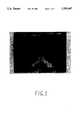
- FIGS. 1 and 2are scanning electron microscopy pictures of a micro-probe tip made in accord with the present invention.
- FIG. 3is a plan view of a micro-probe tip in accord with the present invention.
- a silicon tip on a silicon cantilever substrateis first made in a conventional process, for example as described in U.S. Pat. No. 4,968,585 to the point of forming silicon posts with any cap removed.
- This processinvolves use of semiconductor masking and etching techniques.
- a desired cantilever sectionis laid out on a silicon wafer with an integral tip section. Silicon is etched away in the cantilever section leaving a post at the tip section.
- the postis then sharpened using the technique described by Marcus et al. in Applied Physics Letters 56, no. 3, p. 226 (1990) until a high aspect ratio tip is formed.
- a high aspect ratiois commonly defined as the length of the tip exceeding the dimension of the base by at least five times.
- Final shapingmay be by any suitable method such as ion beam etching of silicon, reactive ion or plasma etching or various wet etch processes, including electrochemical processes.
- the tipwhich is free from oxide at this point is placed in a reactive environment, generally in a partial vacuum and at a temperature in the neighborhood of 1000° C. and the surface of the silicon or other base material is converted into the material of choice.
- the tipis very thin it is possible to convert the critical parts of the tip completely, if so desired, while coating the rest of it with a layer of the reactant material. The conversion process is not dependent on the shaping process which is used.
- SiC tipscan also be formed using acetylene or almost any aliphatic gaseous compound, rather than methane, as the organic reactive gas.
- the method of C. J. Mogab and H. J. Leamy, described in Applied Physics Letters, 45, no. 3, p. 1075 (1974)relates to conversion of monocrystalline silicon to ⁇ -silicon carbide using acetylene in a vacuum of 10 -7 to 5 ⁇ 10 -4 Torr at temperatures between 800° and 1100° C.
- FIGS. 1 and 2show a SiC tip made in accord with our invention using the procedure of Mogab et al., except using propane, C 3 H 8 as the organic reactive gas.
- FIG. 1shows a thinned tip before reacting with a reactive gas.
- FIG. 2shows the same tip after the reacting step. No visible change in the aspect ratio has occurred.
- the tiphas sides that arch upwardly following a curve that appears exponentially steep at the center.
- the height of the tipis more than 5 micrometers and the base dimension is about one micrometer.
- outer zones 13 of tip 11are reacted to form SiC.
- the dimensions A and Bare 200 ⁇ each.
- a rounded tipmay form at apex region 15 having an estimated radius of about 100 ⁇ indicated by arrow R, but conditions for forming rounded tips are not understood and rounding cannot be predicted. The rounding of the tip would give the tip a stylus quality, avoiding tendency to fracture if the tip tapered to a hair-like point, as well as reducing the tendency to stick to material.
- An unreacted silicon zone 17lies beneath the reacted regions.
- the length of the completely converted portionis about 500 ⁇ . Very short reaction times of a few minutes are all that is required to provide almost complete conversion.
- a hard finishinvolves Si 3 N 4 .
- an appropriate source of nitrogensuch as ammonia needs to be used.
- nitrogen gasalthough usable, is less desirable as it does not decompose readily.
- Itcan also be prepared by plasma anodic nitridation in a nitrogen-hydrogen plasma at lower temperatures (700°-900° C.) or in an ammonia plasma.
- plasma nitridationthe silicon tip is placed in a vacuum chamber in the vicinity of a pair of electrodes.
- a nitrogen-containing gas, such as ammonia, NH 3is introduced into the chamber.
- Thermal nitridationis a well established technology in the semiconductor industry. It provides for very good quality films, but usually very thin (50-100 ⁇ ), as the growth kinetics are self-limiting.
- Tips coated with Si 3 N 4are usually non-conducting, as the nitride tends to be a very good insulator under normal conditions. However, its inertness offsets this particular difficulty. Mixtures of oxi-nitrides or carbo-nitrides, prepared with gases which supply oxygen, carbon and nitrogen, are used to vary conductivity, depending on the application for the tips. Other organic vapors may also be reacted with the silicon tips to form the superhard tips of the present invention.
- Tungstenis a material which can be deposited in molecular form on a silicon tip from WF 6 . If the tungsten coated tip is heated without introduction of an organic vapor, tungsten silicide will form and this is a superhard tip material.
- a tungsten carbide tip, WCcan be formed by reacting a tungsten wire in an aliphatic gas in a reaction vessel. The thin tungsten wire may be formed by etching a larger tungsten wire to a fine wire having a desired shape. After etching the wire is reacted as described using an aliphatic compound, such as methane, propane or acetylene.
- Tipswhich are electrically conductive can be used as field emission tips.
- the increased hardnessis expected to provide longer life, as damage from ion impact would be minimized.
Landscapes
- Engineering & Computer Science (AREA)
- Manufacturing & Machinery (AREA)
- Physics & Mathematics (AREA)
- General Physics & Mathematics (AREA)
- Nuclear Medicine, Radiotherapy & Molecular Imaging (AREA)
- Radiology & Medical Imaging (AREA)
- Health & Medical Sciences (AREA)
- General Health & Medical Sciences (AREA)
- Chemical & Material Sciences (AREA)
- Microelectronics & Electronic Packaging (AREA)
- Mechanical Engineering (AREA)
- Nanotechnology (AREA)
- Analytical Chemistry (AREA)
- Crystallography & Structural Chemistry (AREA)
- Carbon And Carbon Compounds (AREA)
- Micromachines (AREA)
- Measurement Of Length, Angles, Or The Like Using Electric Or Magnetic Means (AREA)
Abstract
Description
Claims (20)
Priority Applications (3)
| Application Number | Priority Date | Filing Date | Title |
|---|---|---|---|
| US08/092,780US5393647A (en) | 1993-07-16 | 1993-07-16 | Method of making superhard tips for micro-probe microscopy and field emission |
| PCT/US1994/007925WO1995002894A1 (en) | 1993-07-16 | 1994-07-15 | Superhard tips for micro-probe microscopy and field emission |
| US08/395,410US5658710A (en) | 1993-07-16 | 1995-02-24 | Method of making superhard mechanical microstructures |
Applications Claiming Priority (1)
| Application Number | Priority Date | Filing Date | Title |
|---|---|---|---|
| US08/092,780US5393647A (en) | 1993-07-16 | 1993-07-16 | Method of making superhard tips for micro-probe microscopy and field emission |
Related Child Applications (1)
| Application Number | Title | Priority Date | Filing Date |
|---|---|---|---|
| US08/395,410Continuation-In-PartUS5658710A (en) | 1993-07-16 | 1995-02-24 | Method of making superhard mechanical microstructures |
Publications (1)
| Publication Number | Publication Date |
|---|---|
| US5393647Atrue US5393647A (en) | 1995-02-28 |
Family
ID=22235127
Family Applications (2)
| Application Number | Title | Priority Date | Filing Date |
|---|---|---|---|
| US08/092,780Expired - Fee RelatedUS5393647A (en) | 1993-07-16 | 1993-07-16 | Method of making superhard tips for micro-probe microscopy and field emission |
| US08/395,410Expired - Fee RelatedUS5658710A (en) | 1993-07-16 | 1995-02-24 | Method of making superhard mechanical microstructures |
Family Applications After (1)
| Application Number | Title | Priority Date | Filing Date |
|---|---|---|---|
| US08/395,410Expired - Fee RelatedUS5658710A (en) | 1993-07-16 | 1995-02-24 | Method of making superhard mechanical microstructures |
Country Status (2)
| Country | Link |
|---|---|
| US (2) | US5393647A (en) |
| WO (1) | WO1995002894A1 (en) |
Cited By (78)
| Publication number | Priority date | Publication date | Assignee | Title |
|---|---|---|---|---|
| WO1996003641A1 (en)* | 1994-07-28 | 1996-02-08 | Kley Victor B | Scanning probe microscope assembly |
| US5600200A (en) | 1992-03-16 | 1997-02-04 | Microelectronics And Computer Technology Corporation | Wire-mesh cathode |
| US5601966A (en) | 1993-11-04 | 1997-02-11 | Microelectronics And Computer Technology Corporation | Methods for fabricating flat panel display systems and components |
| US5612712A (en) | 1992-03-16 | 1997-03-18 | Microelectronics And Computer Technology Corporation | Diode structure flat panel display |
| US5656525A (en)* | 1994-12-12 | 1997-08-12 | Industrial Technology Research Institute | Method of manufacturing high aspect-ratio field emitters for flat panel displays |
| US5675216A (en) | 1992-03-16 | 1997-10-07 | Microelectronics And Computer Technololgy Corp. | Amorphic diamond film flat field emission cathode |
| US5747120A (en)* | 1996-03-29 | 1998-05-05 | Regents Of The University Of California | Laser ablated hard coating for microtools |
| US5764673A (en)* | 1995-09-25 | 1998-06-09 | Mitsubishi Denki Kabushiki Kaisha | Semiconductor light emitting device |
| US5767691A (en)* | 1993-12-22 | 1998-06-16 | International Business Machines Corporation | Probe-oxide-semiconductor method and apparatus for measuring oxide charge on a semiconductor wafer |
| US5780851A (en)* | 1996-11-12 | 1998-07-14 | Electronics And Telecommunications Research Institute | Method of forming a diamond on the pointed tip |
| US5861707A (en) | 1991-11-07 | 1999-01-19 | Si Diamond Technology, Inc. | Field emitter with wide band gap emission areas and method of using |
| US5874668A (en) | 1995-10-24 | 1999-02-23 | Arch Development Corporation | Atomic force microscope for biological specimens |
| US5892223A (en)* | 1997-06-30 | 1999-04-06 | Harris Corporation | Multilayer microtip probe and method |
| US5936243A (en)* | 1997-06-09 | 1999-08-10 | Ian Hardcastle | Conductive micro-probe and memory device |
| US5936237A (en)* | 1995-07-05 | 1999-08-10 | Van Der Weide; Daniel Warren | Combined topography and electromagnetic field scanning probe microscope |
| US5985085A (en)* | 1997-10-01 | 1999-11-16 | Arcturus Engineering, Inc. | Method of manufacturing consumable for laser capture microdissection |
| US5989931A (en)* | 1997-09-24 | 1999-11-23 | Simon Fraser University | Low-cost methods for manufacturing field ionization and emission structures with self-aligned gate electrodes |
| US6091124A (en)* | 1996-06-13 | 2000-07-18 | International Business Machines Corporation | Micromechanical sensor for AFM/STM profilometry |
| US6165808A (en)* | 1998-10-06 | 2000-12-26 | Micron Technology, Inc. | Low temperature process for sharpening tapered silicon structures |
| US6184973B1 (en) | 1997-02-07 | 2001-02-06 | Arcturus Engineering, Inc. | Laser capture microdissection pressure plate and transfer arm |
| US6187604B1 (en)* | 1994-09-16 | 2001-02-13 | Micron Technology, Inc. | Method of making field emitters using porous silicon |
| US6265711B1 (en)* | 1994-07-28 | 2001-07-24 | General Nanotechnology L.L.C. | Scanning probe microscope assembly and method for making spectrophotometric near-field optical and scanning measurements |
| US6339217B1 (en)* | 1995-07-28 | 2002-01-15 | General Nanotechnology Llc | Scanning probe microscope assembly and method for making spectrophotometric, near-field, and scanning probe measurements |
| US6400166B2 (en) | 1999-04-15 | 2002-06-04 | International Business Machines Corporation | Micro probe and method of fabricating same |
| US6437329B1 (en) | 1999-10-27 | 2002-08-20 | Advanced Micro Devices, Inc. | Use of carbon nanotubes as chemical sensors by incorporation of fluorescent molecules within the tube |
| US6455847B1 (en) | 2000-04-26 | 2002-09-24 | Advanced Micro Devices, Inc. | Carbon nanotube probes in atomic force microscope to detect partially open/closed contacts |
| US6495195B2 (en) | 1997-02-14 | 2002-12-17 | Arcturus Engineering, Inc. | Broadband absorbing film for laser capture microdissection |
| US6528248B2 (en) | 1999-04-29 | 2003-03-04 | Arcturus Engineering, Inc. | Processing technology for LCM samples |
| US6629869B1 (en) | 1992-03-16 | 2003-10-07 | Si Diamond Technology, Inc. | Method of making flat panel displays having diamond thin film cathode |
| US6633176B2 (en)* | 1998-08-31 | 2003-10-14 | Mitsubishi Denki Kabushiki Kaisha | Semiconductor device test probe having improved tip portion and manufacturing method thereof |
| US6690470B1 (en) | 1999-11-04 | 2004-02-10 | Arcturus Engineering, Inc. | Automated laser capture microdissection |
| US6752008B1 (en) | 2001-03-08 | 2004-06-22 | General Nanotechnology Llc | Method and apparatus for scanning in scanning probe microscopy and presenting results |
| US20040118192A1 (en)* | 2002-09-09 | 2004-06-24 | General Nanotechnology Llc | Fluid delivery for scanning probe microscopy |
| US6787768B1 (en) | 2001-03-08 | 2004-09-07 | General Nanotechnology Llc | Method and apparatus for tool and tip design for nanomachining and measurement |
| US20040189176A1 (en)* | 2003-03-24 | 2004-09-30 | Matsushita Electric Industrial Co., Ltd. | Field-emission electron source, method of manufacturing the same, and image display apparatus |
| US6802646B1 (en) | 2001-04-30 | 2004-10-12 | General Nanotechnology Llc | Low-friction moving interfaces in micromachines and nanomachines |
| US6813937B2 (en) | 2001-11-28 | 2004-11-09 | General Nanotechnology Llc | Method and apparatus for micromachines, microstructures, nanomachines and nanostructures |
| US6865927B1 (en) | 2001-01-30 | 2005-03-15 | General Nanotechnology Llc | Sharpness testing of micro-objects such as miniature diamond tool tips |
| US20050056783A1 (en)* | 1999-07-01 | 2005-03-17 | General Nanotechnology, Llc | Object inspection and/or modification system and method |
| US6880388B1 (en) | 2001-03-08 | 2005-04-19 | General Nanotechnology Llc | Active cantilever for nanomachining and metrology |
| US20050092929A1 (en)* | 2003-07-08 | 2005-05-05 | Schneiker Conrad W. | Integrated sub-nanometer-scale electron beam systems |
| US20050172703A1 (en)* | 1994-07-28 | 2005-08-11 | General Nanotechnology Llc | Scanning probe microscopy inspection and modification system |
| US20050190684A1 (en)* | 1995-07-24 | 2005-09-01 | General Nanotechnology Llc | Nanometer scale data storage device and associated positioning system |
| US7053369B1 (en) | 2001-10-19 | 2006-05-30 | Rave Llc | Scan data collection for better overall data accuracy |
| US20060139621A1 (en)* | 2001-11-05 | 2006-06-29 | Baer Thomas M | Automated microdissection instrument |
| US20060148070A1 (en)* | 1997-10-01 | 2006-07-06 | Baer Thomas M | Consumable for laser capture microdissection |
| US20070025907A1 (en)* | 2005-05-18 | 2007-02-01 | National Research Council Of Canada And University Of Alberta | Nano-tip fabrication by spatially controlled etching |
| US7196328B1 (en) | 2001-03-08 | 2007-03-27 | General Nanotechnology Llc | Nanomachining method and apparatus |
| US20070125160A1 (en)* | 2005-11-15 | 2007-06-07 | The University Of Houston | Short and thin silicon cantilever with tip and fabrication thereof |
| US7253407B1 (en) | 2001-03-08 | 2007-08-07 | General Nanotechnology Llc | Active cantilever for nanomachining and metrology |
| US20080106777A1 (en)* | 2006-11-03 | 2008-05-08 | Weir Michael P | Resonant fourier scanning |
| US20080146898A1 (en)* | 2006-12-19 | 2008-06-19 | Ethicon Endo-Surgery, Inc. | Spectral windows for surgical treatment through intervening fluids |
| US20080151343A1 (en)* | 2006-12-22 | 2008-06-26 | Ethicon Endo-Surgery, Inc. | Apparatus including a scanned beam imager having an optical dome |
| US20080154248A1 (en)* | 2006-12-22 | 2008-06-26 | Ethicon Endo-Surgery, Inc. | Apparatus and method for medically treating a tattoo |
| US20080167546A1 (en)* | 2007-01-09 | 2008-07-10 | Ethicon Endo-Surgery, Inc. | Methods for imaging the anatomy with an anatomically secured scanner assembly |
| US20080173803A1 (en)* | 2007-01-18 | 2008-07-24 | Ethicon Endo-Surgery, Inc. | Scanning beam imaging with adjustable detector sensitivity or gain |
| US20080226029A1 (en)* | 2007-03-12 | 2008-09-18 | Weir Michael P | Medical device including scanned beam unit for imaging and therapy |
| US20080229577A1 (en)* | 2007-03-19 | 2008-09-25 | John Heck | Seek-scan probe (SSP) memory with sharp probe tips formed at CMOS-compatible temperatures |
| US20080255458A1 (en)* | 2007-04-13 | 2008-10-16 | Ethicon Endo-Surgery, Inc. | System and method using fluorescence to examine within a patient's anatomy |
| US20090002794A1 (en)* | 2007-06-29 | 2009-01-01 | Ethicon Endo-Surgery, Inc. | Receiver aperture broadening for scanned beam imaging |
| US7473401B1 (en) | 1997-12-04 | 2009-01-06 | Mds Analytical Technologies (Us) Inc. | Fluidic extraction of microdissected samples |
| US20090015695A1 (en)* | 2007-07-13 | 2009-01-15 | Ethicon Endo-Surgery, Inc. | Sbi motion artifact removal apparatus and method |
| US20090021818A1 (en)* | 2007-07-20 | 2009-01-22 | Ethicon Endo-Surgery, Inc. | Medical scanning assembly with variable image capture and display |
| US20090036734A1 (en)* | 2007-07-31 | 2009-02-05 | Ethicon Endo-Surgery, Inc. | Devices and methods for introducing a scanning beam unit into the anatomy |
| US20090245599A1 (en)* | 2008-03-27 | 2009-10-01 | Ethicon Endo-Surgery, Inc. | Method for creating a pixel image from sampled data of a scanned beam imager |
| US20090270724A1 (en)* | 2008-04-25 | 2009-10-29 | Ethicon Endo-Surgery, Inc. | Scanned beam device and method using same which measures the reflectance of patient tissue |
| US20100077516A1 (en)* | 2008-09-22 | 2010-03-25 | International Business Machines Corporation | Platinum silicide tip apices for probe-based technologies |
| US7925333B2 (en) | 2007-08-28 | 2011-04-12 | Ethicon Endo-Surgery, Inc. | Medical device including scanned beam unit with operational control features |
| US7983739B2 (en) | 2007-08-27 | 2011-07-19 | Ethicon Endo-Surgery, Inc. | Position tracking and control for a scanning assembly |
| US7995045B2 (en) | 2007-04-13 | 2011-08-09 | Ethicon Endo-Surgery, Inc. | Combined SBI and conventional image processor |
| US8160678B2 (en) | 2007-06-18 | 2012-04-17 | Ethicon Endo-Surgery, Inc. | Methods and devices for repairing damaged or diseased tissue using a scanning beam assembly |
| US8216214B2 (en) | 2007-03-12 | 2012-07-10 | Ethicon Endo-Surgery, Inc. | Power modulation of a scanning beam for imaging, therapy, and/or diagnosis |
| US8715955B2 (en) | 2004-09-09 | 2014-05-06 | Life Technologies Corporation | Laser microdissection apparatus and method |
| US8801606B2 (en) | 2007-01-09 | 2014-08-12 | Ethicon Endo-Surgery, Inc. | Method of in vivo monitoring using an imaging system including scanned beam imaging unit |
| US9079762B2 (en) | 2006-09-22 | 2015-07-14 | Ethicon Endo-Surgery, Inc. | Micro-electromechanical device |
| DE102015118805A1 (en)* | 2015-11-03 | 2017-05-04 | Gottfried Wilhelm Leibniz Universität Hannover | Electron emission electrode and method for its production |
| US10156501B2 (en) | 2001-11-05 | 2018-12-18 | Life Technologies Corporation | Automated microdissection instrument for determining a location of a laser beam projection on a worksurface area |
| US11169177B2 (en)* | 2016-08-12 | 2021-11-09 | Tiptek, LLC | Scanning probe and electron microscope probes and their manufacture |
Families Citing this family (50)
| Publication number | Priority date | Publication date | Assignee | Title |
|---|---|---|---|---|
| SE9502258D0 (en)* | 1995-06-21 | 1995-06-21 | Pharmacia Biotech Ab | Method for the manufacture of a membrane-containing microstructure |
| US6200388B1 (en)* | 1998-02-11 | 2001-03-13 | Applied Materials, Inc. | Substrate support for a thermal processing chamber |
| US6171972B1 (en) | 1998-03-17 | 2001-01-09 | Rosemount Aerospace Inc. | Fracture-resistant micromachined devices |
| US6299988B1 (en)* | 1998-04-27 | 2001-10-09 | General Electric Company | Ceramic with preferential oxygen reactive layer |
| US6088463A (en) | 1998-10-30 | 2000-07-11 | Microtronic A/S | Solid state silicon-based condenser microphone |
| US6064145A (en)* | 1999-06-04 | 2000-05-16 | Winbond Electronics Corporation | Fabrication of field emitting tips |
| US6248642B1 (en) | 1999-06-24 | 2001-06-19 | Ibis Technology Corporation | SIMOX using controlled water vapor for oxygen implants |
| US6433342B1 (en) | 1999-08-18 | 2002-08-13 | Ibis Technology Corporation | Coated wafer holding pin |
| US6155436A (en)* | 1999-08-18 | 2000-12-05 | Ibis Technology Corporation | Arc inhibiting wafer holder assembly |
| US6452195B1 (en) | 1999-08-18 | 2002-09-17 | Ibis Technology Corporation | Wafer holding pin |
| US6423975B1 (en) | 1999-08-18 | 2002-07-23 | Ibis Technology, Inc. | Wafer holder for simox processing |
| US7088037B2 (en)* | 1999-09-01 | 2006-08-08 | Micron Technology, Inc. | Field emission display device |
| US6829131B1 (en)* | 1999-09-13 | 2004-12-07 | Carnegie Mellon University | MEMS digital-to-acoustic transducer with error cancellation |
| EP1148758A1 (en)* | 2000-04-18 | 2001-10-24 | THOMSON multimedia S.A. | Cabinet for audio devices |
| US6525864B1 (en) | 2000-07-20 | 2003-02-25 | Nayna Networks, Inc. | Integrated mirror array and circuit device |
| US6527965B1 (en) | 2001-02-09 | 2003-03-04 | Nayna Networks, Inc. | Method for fabricating improved mirror arrays for physical separation |
| US6407844B1 (en) | 2001-02-09 | 2002-06-18 | Nayna Networks, Inc. | Device for fabricating improved mirror arrays for physical separation |
| US6577427B1 (en)* | 2001-02-20 | 2003-06-10 | Nayna Networks, Inc. | Process for manufacturing mirror devices using semiconductor technology |
| US6529654B1 (en) | 2001-05-02 | 2003-03-04 | Nayna Networks, Inc. | Method for transparent switching and controlling optical signals using mirror designs |
| US6688169B2 (en) | 2001-06-15 | 2004-02-10 | Textron Systems Corporation | Systems and methods for sensing an acoustic signal using microelectromechanical systems technology |
| US6771851B1 (en) | 2001-06-19 | 2004-08-03 | Nayna Networks | Fast switching method for a micro-mirror device for optical switching applications |
| WO2003017717A2 (en)* | 2001-08-17 | 2003-02-27 | Carnegie Mellon University | Method and apparatus for reconstruction of soundwaves from digital signals |
| US6477291B1 (en) | 2001-09-13 | 2002-11-05 | Nayna Networks, Inc. | Method and system for in-band connectivity for optical switching applications |
| US6614517B1 (en) | 2001-09-18 | 2003-09-02 | Nayna Networks, Inc. | Method and computer aided apparatus for aligning large density fiber arrays |
| RU2193804C1 (en)* | 2001-10-22 | 2002-11-27 | Санкт-Петербургский государственный электротехнический университет | Thermomechanical semiconductor microactuator |
| US6836353B1 (en) | 2001-11-20 | 2004-12-28 | Nayna Networks, Inc. | Redundant switch fabric methods and system for switching of telecommunication signals |
| US20030210799A1 (en)* | 2002-05-10 | 2003-11-13 | Gabriel Kaigham J. | Multiple membrane structure and method of manufacture |
| US7142682B2 (en)* | 2002-12-20 | 2006-11-28 | Sonion Mems A/S | Silicon-based transducer for use in hearing instruments and listening devices |
| US7049051B2 (en)* | 2003-01-23 | 2006-05-23 | Akustica, Inc. | Process for forming and acoustically connecting structures on a substrate |
| US6936524B2 (en)* | 2003-11-05 | 2005-08-30 | Akustica, Inc. | Ultrathin form factor MEMS microphones and microspeakers |
| US7795695B2 (en) | 2005-01-27 | 2010-09-14 | Analog Devices, Inc. | Integrated microphone |
| US7885423B2 (en) | 2005-04-25 | 2011-02-08 | Analog Devices, Inc. | Support apparatus for microphone diaphragm |
| US20070071268A1 (en)* | 2005-08-16 | 2007-03-29 | Analog Devices, Inc. | Packaged microphone with electrically coupled lid |
| US7449356B2 (en)* | 2005-04-25 | 2008-11-11 | Analog Devices, Inc. | Process of forming a microphone using support member |
| US7825484B2 (en)* | 2005-04-25 | 2010-11-02 | Analog Devices, Inc. | Micromachined microphone and multisensor and method for producing same |
| US20070040231A1 (en)* | 2005-08-16 | 2007-02-22 | Harney Kieran P | Partially etched leadframe packages having different top and bottom topologies |
| US7961897B2 (en)* | 2005-08-23 | 2011-06-14 | Analog Devices, Inc. | Microphone with irregular diaphragm |
| WO2007024909A1 (en)* | 2005-08-23 | 2007-03-01 | Analog Devices, Inc. | Multi-microphone system |
| WO2008003051A2 (en)* | 2006-06-29 | 2008-01-03 | Analog Devices, Inc. | Stress mitigation in packaged microchips |
| EP2044802B1 (en)* | 2006-07-25 | 2013-03-27 | Analog Devices, Inc. | Multiple microphone system |
| US20080175425A1 (en)* | 2006-11-30 | 2008-07-24 | Analog Devices, Inc. | Microphone System with Silicon Microphone Secured to Package Lid |
| US7694610B2 (en)* | 2007-06-27 | 2010-04-13 | Siemens Medical Solutions Usa, Inc. | Photo-multiplier tube removal tool |
| US8841738B2 (en) | 2012-10-01 | 2014-09-23 | Invensense, Inc. | MEMS microphone system for harsh environments |
| US9676614B2 (en) | 2013-02-01 | 2017-06-13 | Analog Devices, Inc. | MEMS device with stress relief structures |
| US9108842B2 (en)* | 2013-07-19 | 2015-08-18 | Freescale Semiconductor, Inc. | Reducing microelectromechanical systems stiction by formation of a silicon carbide layer |
| US10167189B2 (en) | 2014-09-30 | 2019-01-01 | Analog Devices, Inc. | Stress isolation platform for MEMS devices |
| US20160230570A1 (en) | 2015-02-11 | 2016-08-11 | Rolls-Royce High Temperature Composites Inc. | Modified atmosphere melt infiltration |
| US10131538B2 (en) | 2015-09-14 | 2018-11-20 | Analog Devices, Inc. | Mechanically isolated MEMS device |
| US11417611B2 (en) | 2020-02-25 | 2022-08-16 | Analog Devices International Unlimited Company | Devices and methods for reducing stress on circuit components |
| US11981560B2 (en) | 2020-06-09 | 2024-05-14 | Analog Devices, Inc. | Stress-isolated MEMS device comprising substrate having cavity and method of manufacture |
Citations (10)
| Publication number | Priority date | Publication date | Assignee | Title |
|---|---|---|---|---|
| US4123571A (en)* | 1977-09-08 | 1978-10-31 | International Business Machines Corporation | Method for forming smooth self limiting and pin hole free SiC films on Si |
| US4685996A (en)* | 1986-10-14 | 1987-08-11 | Busta Heinz H | Method of making micromachined refractory metal field emitters |
| US4916002A (en)* | 1989-01-13 | 1990-04-10 | The Board Of Trustees Of The Leland Jr. University | Microcasting of microminiature tips |
| EP0363134A1 (en)* | 1988-10-03 | 1990-04-11 | The Boc Group, Inc. | Formation of refractory metal silicide layers |
| US4968585A (en)* | 1989-06-20 | 1990-11-06 | The Board Of Trustees Of The Leland Stanford Jr. University | Microfabricated cantilever stylus with integrated conical tip |
| US5015323A (en)* | 1989-10-10 | 1991-05-14 | The United States Of America As Represented By The Secretary Of Commerce | Multi-tipped field-emission tool for nanostructure fabrication |
| US5032545A (en)* | 1990-10-30 | 1991-07-16 | Micron Technology, Inc. | Process for preventing a native oxide from forming on the surface of a semiconductor material and integrated circuit capacitors produced thereby |
| US5051379A (en)* | 1989-08-16 | 1991-09-24 | International Business Machines Corporation | Method of producing micromechanical sensors for the AFM/STM profilometry and micromechanical AFM/STM sensor head |
| US5077091A (en)* | 1989-02-16 | 1991-12-31 | Nitruvid | Deposition process in the vapour phase at low temperature of a ceramic coating of the metallic nitride or carbonitride type |
| US5201992A (en)* | 1990-07-12 | 1993-04-13 | Bell Communications Research, Inc. | Method for making tapered microminiature silicon structures |
Family Cites Families (3)
| Publication number | Priority date | Publication date | Assignee | Title |
|---|---|---|---|---|
| US5332697A (en)* | 1989-05-31 | 1994-07-26 | Smith Rosemary L | Formation of silicon nitride by nitridation of porous silicon |
| US4968641A (en)* | 1989-06-22 | 1990-11-06 | Alexander Kalnitsky | Method for formation of an isolating oxide layer |
| US5179499A (en)* | 1992-04-14 | 1993-01-12 | Cornell Research Foundation, Inc. | Multi-dimensional precision micro-actuator |
- 1993
- 1993-07-16USUS08/092,780patent/US5393647A/ennot_activeExpired - Fee Related
- 1994
- 1994-07-15WOPCT/US1994/007925patent/WO1995002894A1/enactiveApplication Filing
- 1995
- 1995-02-24USUS08/395,410patent/US5658710A/ennot_activeExpired - Fee Related
Patent Citations (10)
| Publication number | Priority date | Publication date | Assignee | Title |
|---|---|---|---|---|
| US4123571A (en)* | 1977-09-08 | 1978-10-31 | International Business Machines Corporation | Method for forming smooth self limiting and pin hole free SiC films on Si |
| US4685996A (en)* | 1986-10-14 | 1987-08-11 | Busta Heinz H | Method of making micromachined refractory metal field emitters |
| EP0363134A1 (en)* | 1988-10-03 | 1990-04-11 | The Boc Group, Inc. | Formation of refractory metal silicide layers |
| US4916002A (en)* | 1989-01-13 | 1990-04-10 | The Board Of Trustees Of The Leland Jr. University | Microcasting of microminiature tips |
| US5077091A (en)* | 1989-02-16 | 1991-12-31 | Nitruvid | Deposition process in the vapour phase at low temperature of a ceramic coating of the metallic nitride or carbonitride type |
| US4968585A (en)* | 1989-06-20 | 1990-11-06 | The Board Of Trustees Of The Leland Stanford Jr. University | Microfabricated cantilever stylus with integrated conical tip |
| US5051379A (en)* | 1989-08-16 | 1991-09-24 | International Business Machines Corporation | Method of producing micromechanical sensors for the AFM/STM profilometry and micromechanical AFM/STM sensor head |
| US5015323A (en)* | 1989-10-10 | 1991-05-14 | The United States Of America As Represented By The Secretary Of Commerce | Multi-tipped field-emission tool for nanostructure fabrication |
| US5201992A (en)* | 1990-07-12 | 1993-04-13 | Bell Communications Research, Inc. | Method for making tapered microminiature silicon structures |
| US5032545A (en)* | 1990-10-30 | 1991-07-16 | Micron Technology, Inc. | Process for preventing a native oxide from forming on the surface of a semiconductor material and integrated circuit capacitors produced thereby |
Non-Patent Citations (8)
| Title |
|---|
| Graul et al., "Growth Mechanism of Polycrystalline B-SiC Layers on Silicon Substrate", Appl. Phys. Lett., vol. 21, No. 2 pp. 67-69 (1972). |
| Graul et al., Growth Mechanism of Polycrystalline B SiC Layers on Silicon Substrate , Appl. Phys. Lett., vol. 21, No. 2 pp. 67 69 (1972).* |
| H. J. Kim et al., "Physical and Chemical Nature of Films Formed on Si(100) Surfaces Subjected to C2 H4 at Elevated Temperatures", J. Electrochem. Soc. vol. 134 (9), pp. 2269-2275 (1987). |
| H. J. Kim et al., Physical and Chemical Nature of Films Formed on Si(100) Surfaces Subjected to C 2 H 4 at Elevated Temperatures , J. Electrochem. Soc. vol. 134 (9), pp. 2269 2275 (1987).* |
| Mogab et al., "Conversion of Si to Epitaxial SiC by Reaction with C2 H2", J. Appl. Phys., vol. 45, No. 3, pp. 1075-1084 (1974). |
| Mogab et al., Conversion of Si to Epitaxial SiC by Reaction with C 2 H 2 , J. Appl. Phys., vol. 45, No. 3, pp. 1075 1084 (1974).* |
| T. R. Albrecht et al., "Microfabrication of Cantilever Styli for the Atomic Force Microscope", J. Vac. Sci. Technol. A vol. 8 (4), pp. 3386-3396 (1990). |
| T. R. Albrecht et al., Microfabrication of Cantilever Styli for the Atomic Force Microscope , J. Vac. Sci. Technol. A vol. 8 (4), pp. 3386 3396 (1990).* |
Cited By (161)
| Publication number | Priority date | Publication date | Assignee | Title |
|---|---|---|---|---|
| US5861707A (en) | 1991-11-07 | 1999-01-19 | Si Diamond Technology, Inc. | Field emitter with wide band gap emission areas and method of using |
| US5600200A (en) | 1992-03-16 | 1997-02-04 | Microelectronics And Computer Technology Corporation | Wire-mesh cathode |
| US5612712A (en) | 1992-03-16 | 1997-03-18 | Microelectronics And Computer Technology Corporation | Diode structure flat panel display |
| US6629869B1 (en) | 1992-03-16 | 2003-10-07 | Si Diamond Technology, Inc. | Method of making flat panel displays having diamond thin film cathode |
| US5675216A (en) | 1992-03-16 | 1997-10-07 | Microelectronics And Computer Technololgy Corp. | Amorphic diamond film flat field emission cathode |
| US5686791A (en) | 1992-03-16 | 1997-11-11 | Microelectronics And Computer Technology Corp. | Amorphic diamond film flat field emission cathode |
| US5601966A (en) | 1993-11-04 | 1997-02-11 | Microelectronics And Computer Technology Corporation | Methods for fabricating flat panel display systems and components |
| US5614353A (en) | 1993-11-04 | 1997-03-25 | Si Diamond Technology, Inc. | Methods for fabricating flat panel display systems and components |
| US5652083A (en) | 1993-11-04 | 1997-07-29 | Microelectronics And Computer Technology Corporation | Methods for fabricating flat panel display systems and components |
| US5767691A (en)* | 1993-12-22 | 1998-06-16 | International Business Machines Corporation | Probe-oxide-semiconductor method and apparatus for measuring oxide charge on a semiconductor wafer |
| US7091476B2 (en) | 1994-07-28 | 2006-08-15 | General Nanotechnology Llc | Scanning probe microscope assembly |
| US7045780B2 (en) | 1994-07-28 | 2006-05-16 | General Nanotechnology, Llc | Scanning probe microscopy inspection and modification system |
| US20060237639A1 (en)* | 1994-07-28 | 2006-10-26 | General Nanotechnology Llc | Scanning probe microscope assembly and method for making spectrophotometric, near-filed, and scanning probe measurements |
| US7485856B2 (en) | 1994-07-28 | 2009-02-03 | General Nanotechnology Llp | Scanning probe microscopy inspection and modification system |
| US6396054B1 (en) | 1994-07-28 | 2002-05-28 | General Nanotechnology Llc | Scanning probe microscope assembly and method for making confocal, spectrophotometric, near-field, and scanning probe measurements and associated images |
| US7615738B2 (en) | 1994-07-28 | 2009-11-10 | General Nanotechnology, Llc | Scanning probe microscope assembly and method for making spectrophotometric, near-field, and scanning probe measurements |
| US20070022804A1 (en)* | 1994-07-28 | 2007-02-01 | General Nanotechnology Llc | Scanning probe microscopy inspection and modification system |
| US6265711B1 (en)* | 1994-07-28 | 2001-07-24 | General Nanotechnology L.L.C. | Scanning probe microscope assembly and method for making spectrophotometric near-field optical and scanning measurements |
| US6369379B1 (en) | 1994-07-28 | 2002-04-09 | General Nanotechnology Llc | Scanning probe microscope assembly and method for making confocal, spectrophotometric, near-field, and scanning probe measurements and associated images |
| US6515277B1 (en) | 1994-07-28 | 2003-02-04 | General Nanotechnology L.L.C. | Scanning probe microscope assembly and method for making confocal, spectrophotometric, near-field, and scanning probe measurements and associated images |
| WO1996003641A1 (en)* | 1994-07-28 | 1996-02-08 | Kley Victor B | Scanning probe microscope assembly |
| US20050172703A1 (en)* | 1994-07-28 | 2005-08-11 | General Nanotechnology Llc | Scanning probe microscopy inspection and modification system |
| US6620640B2 (en) | 1994-09-16 | 2003-09-16 | Micron Technology, Inc. | Method of making field emitters |
| US6187604B1 (en)* | 1994-09-16 | 2001-02-13 | Micron Technology, Inc. | Method of making field emitters using porous silicon |
| US6426234B2 (en) | 1994-09-16 | 2002-07-30 | Micron Technology, Inc. | Method of making field emitters using porous silicon |
| US5656525A (en)* | 1994-12-12 | 1997-08-12 | Industrial Technology Research Institute | Method of manufacturing high aspect-ratio field emitters for flat panel displays |
| US5936237A (en)* | 1995-07-05 | 1999-08-10 | Van Der Weide; Daniel Warren | Combined topography and electromagnetic field scanning probe microscope |
| US20060239129A1 (en)* | 1995-07-24 | 2006-10-26 | General Nanotechnology Llc | Nanometer scale data storage device and associated positioning system |
| US7042828B2 (en) | 1995-07-24 | 2006-05-09 | General Nanotechnology Llc | Nanometer scale data storage device and associated positioning system |
| US7535817B2 (en) | 1995-07-24 | 2009-05-19 | General Nanotechnology, L.L.C. | Nanometer scale data storage device and associated positioning system |
| US20050190684A1 (en)* | 1995-07-24 | 2005-09-01 | General Nanotechnology Llc | Nanometer scale data storage device and associated positioning system |
| US6339217B1 (en)* | 1995-07-28 | 2002-01-15 | General Nanotechnology Llc | Scanning probe microscope assembly and method for making spectrophotometric, near-field, and scanning probe measurements |
| US5764673A (en)* | 1995-09-25 | 1998-06-09 | Mitsubishi Denki Kabushiki Kaisha | Semiconductor light emitting device |
| US5874668A (en) | 1995-10-24 | 1999-02-23 | Arch Development Corporation | Atomic force microscope for biological specimens |
| US5747120A (en)* | 1996-03-29 | 1998-05-05 | Regents Of The University Of California | Laser ablated hard coating for microtools |
| US6091124A (en)* | 1996-06-13 | 2000-07-18 | International Business Machines Corporation | Micromechanical sensor for AFM/STM profilometry |
| US5780851A (en)* | 1996-11-12 | 1998-07-14 | Electronics And Telecommunications Research Institute | Method of forming a diamond on the pointed tip |
| US20040027556A1 (en)* | 1997-02-07 | 2004-02-12 | Baer Thomas M. | Laser capture microdissection translation stage joystick |
| US6697149B2 (en) | 1997-02-07 | 2004-02-24 | Arcturus Engineering, Inc. | Laser capture microdissection vacuum hold-down |
| US7012676B2 (en) | 1997-02-07 | 2006-03-14 | Arcturus Bioscience, Inc. | Laser capture microdissection translation stage joystick |
| US6215550B1 (en) | 1997-02-07 | 2001-04-10 | Arcturus Engineering, Inc. | Laser capture microdissection optical system |
| US6184973B1 (en) | 1997-02-07 | 2001-02-06 | Arcturus Engineering, Inc. | Laser capture microdissection pressure plate and transfer arm |
| US6512576B1 (en) | 1997-02-07 | 2003-01-28 | Arcturus Engineering, Inc. | Laser capture microdissection optical system |
| US20040106206A1 (en)* | 1997-02-07 | 2004-06-03 | Baer Thomas M. | Laser capture microdissection vacuum hold-down |
| US6639657B2 (en) | 1997-02-07 | 2003-10-28 | Arcturus Engineering, Inc. | Laser capture microdissection translation stage joystick |
| US6469779B2 (en) | 1997-02-07 | 2002-10-22 | Arcturus Engineering, Inc. | Laser capture microdissection method and apparatus |
| US6924889B2 (en) | 1997-02-07 | 2005-08-02 | Arcturus Bioscience, Inc. | Laser capture microdissection vacuum hold-down |
| US6700653B2 (en) | 1997-02-07 | 2004-03-02 | Arcturus Engineering, Inc. | Laser capture microdissection optical system |
| US20030031781A1 (en)* | 1997-02-14 | 2003-02-13 | Baer Thomas M. | Broadband absorbing film for laser capture microdissection |
| US6495195B2 (en) | 1997-02-14 | 2002-12-17 | Arcturus Engineering, Inc. | Broadband absorbing film for laser capture microdissection |
| US5936243A (en)* | 1997-06-09 | 1999-08-10 | Ian Hardcastle | Conductive micro-probe and memory device |
| US5892223A (en)* | 1997-06-30 | 1999-04-06 | Harris Corporation | Multilayer microtip probe and method |
| US5989931A (en)* | 1997-09-24 | 1999-11-23 | Simon Fraser University | Low-cost methods for manufacturing field ionization and emission structures with self-aligned gate electrodes |
| US5985085A (en)* | 1997-10-01 | 1999-11-16 | Arcturus Engineering, Inc. | Method of manufacturing consumable for laser capture microdissection |
| US20060148070A1 (en)* | 1997-10-01 | 2006-07-06 | Baer Thomas M | Consumable for laser capture microdissection |
| US7221447B2 (en) | 1997-10-01 | 2007-05-22 | Molecular Devices Corporation | Consumable for laser capture microdissection |
| US7075640B2 (en) | 1997-10-01 | 2006-07-11 | Arcturus Bioscience, Inc. | Consumable for laser capture microdissection |
| US7473401B1 (en) | 1997-12-04 | 2009-01-06 | Mds Analytical Technologies (Us) Inc. | Fluidic extraction of microdissected samples |
| US10610995B2 (en) | 1998-01-21 | 2020-04-07 | Victor B. Kley | Method and apparatus for nanolapping |
| US6633176B2 (en)* | 1998-08-31 | 2003-10-14 | Mitsubishi Denki Kabushiki Kaisha | Semiconductor device test probe having improved tip portion and manufacturing method thereof |
| US20060038575A1 (en)* | 1998-08-31 | 2006-02-23 | Mitsubishi Denki Kabushiki Kaisha | Semiconductor device test probe |
| US7274195B2 (en) | 1998-08-31 | 2007-09-25 | Mitsubishi Denki Kabushiki Kaisha | Semiconductor device test probe |
| US20050189955A1 (en)* | 1998-08-31 | 2005-09-01 | Mitsubishi Denki Kabushiki Kaisha | Semiconductor device test probe having improved tip portion |
| US7276923B2 (en) | 1998-08-31 | 2007-10-02 | Mitsubishi Denki Kabushiki Kaisha | Semiconductor device test probe |
| US20030129777A1 (en)* | 1998-10-06 | 2003-07-10 | Tianhong Zhang | Process for sharpening tapered silicon structures |
| US6953701B2 (en) | 1998-10-06 | 2005-10-11 | Micron Technology, Inc. | Process for sharpening tapered silicon structures |
| US7078249B2 (en) | 1998-10-06 | 2006-07-18 | Micron Technology, Inc. | Process for forming sharp silicon structures |
| US6165808A (en)* | 1998-10-06 | 2000-12-26 | Micron Technology, Inc. | Low temperature process for sharpening tapered silicon structures |
| US6440762B1 (en) | 1998-10-06 | 2002-08-27 | Micron Technology, Inc. | Low temperature process for sharpening tapered silicon structures |
| US6400166B2 (en) | 1999-04-15 | 2002-06-04 | International Business Machines Corporation | Micro probe and method of fabricating same |
| US6528248B2 (en) | 1999-04-29 | 2003-03-04 | Arcturus Engineering, Inc. | Processing technology for LCM samples |
| US7109482B2 (en) | 1999-07-01 | 2006-09-19 | General Nanotechnology Llc | Object inspection and/or modification system and method |
| US20050056783A1 (en)* | 1999-07-01 | 2005-03-17 | General Nanotechnology, Llc | Object inspection and/or modification system and method |
| US6437329B1 (en) | 1999-10-27 | 2002-08-20 | Advanced Micro Devices, Inc. | Use of carbon nanotubes as chemical sensors by incorporation of fluorescent molecules within the tube |
| US20060114456A1 (en)* | 1999-11-04 | 2006-06-01 | Baer Thomas M | Automated laser capture microdissection |
| US20050089949A1 (en)* | 1999-11-04 | 2005-04-28 | Baer Thomas M. | Automated laser capture microdissection |
| US6690470B1 (en) | 1999-11-04 | 2004-02-10 | Arcturus Engineering, Inc. | Automated laser capture microdissection |
| US7027133B2 (en) | 1999-11-04 | 2006-04-11 | Arcturus Bioscience, Inc. | Automated laser capture microdissection |
| US7148966B2 (en) | 1999-11-04 | 2006-12-12 | Arcturus Bioscience, Inc. | Automated laser capture microdissection |
| US6870625B1 (en) | 1999-11-04 | 2005-03-22 | Arcturus Bioscience, Inc. | Automated laser capture microdissection |
| US6455847B1 (en) | 2000-04-26 | 2002-09-24 | Advanced Micro Devices, Inc. | Carbon nanotube probes in atomic force microscope to detect partially open/closed contacts |
| US6931710B2 (en) | 2001-01-30 | 2005-08-23 | General Nanotechnology Llc | Manufacturing of micro-objects such as miniature diamond tool tips |
| US6865927B1 (en) | 2001-01-30 | 2005-03-15 | General Nanotechnology Llc | Sharpness testing of micro-objects such as miniature diamond tool tips |
| US20050115047A1 (en)* | 2001-01-30 | 2005-06-02 | General Nanotechnology Llc | Manufacturing of micro-objects such as miniature diamond tool tips |
| US7178387B1 (en) | 2001-03-08 | 2007-02-20 | General Nanotechnology Llc | Method and apparatus for scanning in scanning probe microscopy and presenting results |
| US6752008B1 (en) | 2001-03-08 | 2004-06-22 | General Nanotechnology Llc | Method and apparatus for scanning in scanning probe microscopy and presenting results |
| US6880388B1 (en) | 2001-03-08 | 2005-04-19 | General Nanotechnology Llc | Active cantilever for nanomachining and metrology |
| US6787768B1 (en) | 2001-03-08 | 2004-09-07 | General Nanotechnology Llc | Method and apparatus for tool and tip design for nanomachining and measurement |
| US7253407B1 (en) | 2001-03-08 | 2007-08-07 | General Nanotechnology Llc | Active cantilever for nanomachining and metrology |
| US7137292B1 (en) | 2001-03-08 | 2006-11-21 | General Nanotechnology Llc | Active cantilever for nanomachining and metrology |
| US6923044B1 (en) | 2001-03-08 | 2005-08-02 | General Nanotechnology Llc | Active cantilever for nanomachining and metrology |
| US7947952B1 (en) | 2001-03-08 | 2011-05-24 | General Nanotechnology Llc | Nanomachining method and apparatus |
| US7196328B1 (en) | 2001-03-08 | 2007-03-27 | General Nanotechnology Llc | Nanomachining method and apparatus |
| US6802646B1 (en) | 2001-04-30 | 2004-10-12 | General Nanotechnology Llc | Low-friction moving interfaces in micromachines and nanomachines |
| US20050058384A1 (en)* | 2001-04-30 | 2005-03-17 | General Nanotechnology Llc | Low-friction moving interfaces in micromachines and nanomachines |
| US7053369B1 (en) | 2001-10-19 | 2006-05-30 | Rave Llc | Scan data collection for better overall data accuracy |
| US7547882B2 (en) | 2001-10-19 | 2009-06-16 | Rave Llc | Scan data collection for better overall data accurancy |
| US20060174384A1 (en)* | 2001-10-19 | 2006-08-03 | Rave Llc | Scan data collection for better overall data accurancy |
| US10156501B2 (en) | 2001-11-05 | 2018-12-18 | Life Technologies Corporation | Automated microdissection instrument for determining a location of a laser beam projection on a worksurface area |
| US20060139621A1 (en)* | 2001-11-05 | 2006-06-29 | Baer Thomas M | Automated microdissection instrument |
| US8722357B2 (en) | 2001-11-05 | 2014-05-13 | Life Technologies Corporation | Automated microdissection instrument |
| US20050172739A1 (en)* | 2001-11-28 | 2005-08-11 | General Nanotechnology Llc | Method and apparatus for micromachines, microstructures, nanomachines and nanostructures |
| US7631549B1 (en) | 2001-11-28 | 2009-12-15 | General Nanotechnology Llc | Method and apparatus for micromachines, microstructures, nanomachines and nanostructures |
| US6813937B2 (en) | 2001-11-28 | 2004-11-09 | General Nanotechnology Llc | Method and apparatus for micromachines, microstructures, nanomachines and nanostructures |
| US7266998B2 (en) | 2001-11-28 | 2007-09-11 | General Nanotechnology Llc | Method and apparatus for micromachines, microstructures, nanomachines and nanostructures |
| US9075082B2 (en) | 2002-03-07 | 2015-07-07 | Victor B. Kley | Fluid delivery for scanning probe microscopy |
| US6998689B2 (en) | 2002-09-09 | 2006-02-14 | General Nanotechnology Llc | Fluid delivery for scanning probe microscopy |
| US20040118192A1 (en)* | 2002-09-09 | 2004-06-24 | General Nanotechnology Llc | Fluid delivery for scanning probe microscopy |
| US7588475B2 (en) | 2003-03-24 | 2009-09-15 | Panasonic Corporation | Field-emission electron source, method of manufacturing the same, and image display apparatus |
| US20040189176A1 (en)* | 2003-03-24 | 2004-09-30 | Matsushita Electric Industrial Co., Ltd. | Field-emission electron source, method of manufacturing the same, and image display apparatus |
| US7215072B2 (en)* | 2003-03-24 | 2007-05-08 | Matsushita Electric Industrial Co., Ltd. | Field-emission electron source, method of manufacturing the same, and image display apparatus |
| US20070184747A1 (en)* | 2003-03-24 | 2007-08-09 | Matsushita Electric Industrial Co., Ltd. | Field-emission electron source, method of manufacturing the same, and image display apparatus |
| US7279686B2 (en) | 2003-07-08 | 2007-10-09 | Biomed Solutions, Llc | Integrated sub-nanometer-scale electron beam systems |
| US20050092929A1 (en)* | 2003-07-08 | 2005-05-05 | Schneiker Conrad W. | Integrated sub-nanometer-scale electron beam systems |
| US8715955B2 (en) | 2004-09-09 | 2014-05-06 | Life Technologies Corporation | Laser microdissection apparatus and method |
| US10605706B2 (en) | 2004-09-25 | 2020-03-31 | Life Technologies Corporation | Automated microdissection instrument with controlled focusing during movement of a laser beam across a tissue sample |
| US12372440B2 (en) | 2004-09-25 | 2025-07-29 | Life Technologies Corporation | Automated microdissection instrument and method for processing a biological sample |
| US11703428B2 (en) | 2004-09-25 | 2023-07-18 | Life Technologies Corporation | Automated microdissection instrument and method for processing a biological sample |
| US11175203B2 (en) | 2004-09-25 | 2021-11-16 | Life Technologies Corporation | Automated microdissection instrument using tracking information |
| US7431856B2 (en)* | 2005-05-18 | 2008-10-07 | National Research Council Of Canada | Nano-tip fabrication by spatially controlled etching |
| US20070025907A1 (en)* | 2005-05-18 | 2007-02-01 | National Research Council Of Canada And University Of Alberta | Nano-tip fabrication by spatially controlled etching |
| US7637960B2 (en)* | 2005-11-15 | 2009-12-29 | University Of Houston | Short and thin silicon cantilever with tip and fabrication thereof |
| US20070125160A1 (en)* | 2005-11-15 | 2007-06-07 | The University Of Houston | Short and thin silicon cantilever with tip and fabrication thereof |
| US9079762B2 (en) | 2006-09-22 | 2015-07-14 | Ethicon Endo-Surgery, Inc. | Micro-electromechanical device |
| US20080106777A1 (en)* | 2006-11-03 | 2008-05-08 | Weir Michael P | Resonant fourier scanning |
| US7561317B2 (en) | 2006-11-03 | 2009-07-14 | Ethicon Endo-Surgery, Inc. | Resonant Fourier scanning |
| US20080146898A1 (en)* | 2006-12-19 | 2008-06-19 | Ethicon Endo-Surgery, Inc. | Spectral windows for surgical treatment through intervening fluids |
| US20080151343A1 (en)* | 2006-12-22 | 2008-06-26 | Ethicon Endo-Surgery, Inc. | Apparatus including a scanned beam imager having an optical dome |
| US20080154248A1 (en)* | 2006-12-22 | 2008-06-26 | Ethicon Endo-Surgery, Inc. | Apparatus and method for medically treating a tattoo |
| US7713265B2 (en) | 2006-12-22 | 2010-05-11 | Ethicon Endo-Surgery, Inc. | Apparatus and method for medically treating a tattoo |
| US20080167546A1 (en)* | 2007-01-09 | 2008-07-10 | Ethicon Endo-Surgery, Inc. | Methods for imaging the anatomy with an anatomically secured scanner assembly |
| US8801606B2 (en) | 2007-01-09 | 2014-08-12 | Ethicon Endo-Surgery, Inc. | Method of in vivo monitoring using an imaging system including scanned beam imaging unit |
| US8273015B2 (en) | 2007-01-09 | 2012-09-25 | Ethicon Endo-Surgery, Inc. | Methods for imaging the anatomy with an anatomically secured scanner assembly |
| US7589316B2 (en) | 2007-01-18 | 2009-09-15 | Ethicon Endo-Surgery, Inc. | Scanning beam imaging with adjustable detector sensitivity or gain |
| US20080173803A1 (en)* | 2007-01-18 | 2008-07-24 | Ethicon Endo-Surgery, Inc. | Scanning beam imaging with adjustable detector sensitivity or gain |
| US8216214B2 (en) | 2007-03-12 | 2012-07-10 | Ethicon Endo-Surgery, Inc. | Power modulation of a scanning beam for imaging, therapy, and/or diagnosis |
| US20080226029A1 (en)* | 2007-03-12 | 2008-09-18 | Weir Michael P | Medical device including scanned beam unit for imaging and therapy |
| US8681596B2 (en) | 2007-03-19 | 2014-03-25 | Intel Corporation | Seek-scan probe (SSP) memory with sharp probe tips formed at CMOS-compatible temperatures |
| US20110078835A1 (en)* | 2007-03-19 | 2011-03-31 | Intel Corporation | Seek-scan probe (ssp) memory with sharp probe tips formed at cmos-compatible temperatures |
| US7869334B2 (en)* | 2007-03-19 | 2011-01-11 | Intel Corporation | Seek-scan probe (SSP) memory with sharp probe tips formed at CMOS-compatible temperatures |
| US20080229577A1 (en)* | 2007-03-19 | 2008-09-25 | John Heck | Seek-scan probe (SSP) memory with sharp probe tips formed at CMOS-compatible temperatures |
| US7995045B2 (en) | 2007-04-13 | 2011-08-09 | Ethicon Endo-Surgery, Inc. | Combined SBI and conventional image processor |
| US20080255458A1 (en)* | 2007-04-13 | 2008-10-16 | Ethicon Endo-Surgery, Inc. | System and method using fluorescence to examine within a patient's anatomy |
| US8626271B2 (en) | 2007-04-13 | 2014-01-07 | Ethicon Endo-Surgery, Inc. | System and method using fluorescence to examine within a patient's anatomy |
| US8160678B2 (en) | 2007-06-18 | 2012-04-17 | Ethicon Endo-Surgery, Inc. | Methods and devices for repairing damaged or diseased tissue using a scanning beam assembly |
| US20090002794A1 (en)* | 2007-06-29 | 2009-01-01 | Ethicon Endo-Surgery, Inc. | Receiver aperture broadening for scanned beam imaging |
| US20090015695A1 (en)* | 2007-07-13 | 2009-01-15 | Ethicon Endo-Surgery, Inc. | Sbi motion artifact removal apparatus and method |
| US7982776B2 (en) | 2007-07-13 | 2011-07-19 | Ethicon Endo-Surgery, Inc. | SBI motion artifact removal apparatus and method |
| US20090021818A1 (en)* | 2007-07-20 | 2009-01-22 | Ethicon Endo-Surgery, Inc. | Medical scanning assembly with variable image capture and display |
| US9125552B2 (en) | 2007-07-31 | 2015-09-08 | Ethicon Endo-Surgery, Inc. | Optical scanning module and means for attaching the module to medical instruments for introducing the module into the anatomy |
| US20090036734A1 (en)* | 2007-07-31 | 2009-02-05 | Ethicon Endo-Surgery, Inc. | Devices and methods for introducing a scanning beam unit into the anatomy |
| US7983739B2 (en) | 2007-08-27 | 2011-07-19 | Ethicon Endo-Surgery, Inc. | Position tracking and control for a scanning assembly |
| US7925333B2 (en) | 2007-08-28 | 2011-04-12 | Ethicon Endo-Surgery, Inc. | Medical device including scanned beam unit with operational control features |
| US20090245599A1 (en)* | 2008-03-27 | 2009-10-01 | Ethicon Endo-Surgery, Inc. | Method for creating a pixel image from sampled data of a scanned beam imager |
| US8050520B2 (en) | 2008-03-27 | 2011-11-01 | Ethicon Endo-Surgery, Inc. | Method for creating a pixel image from sampled data of a scanned beam imager |
| US20090270724A1 (en)* | 2008-04-25 | 2009-10-29 | Ethicon Endo-Surgery, Inc. | Scanned beam device and method using same which measures the reflectance of patient tissue |
| US8332014B2 (en) | 2008-04-25 | 2012-12-11 | Ethicon Endo-Surgery, Inc. | Scanned beam device and method using same which measures the reflectance of patient tissue |
| US20100077516A1 (en)* | 2008-09-22 | 2010-03-25 | International Business Machines Corporation | Platinum silicide tip apices for probe-based technologies |
| US8332961B2 (en)* | 2008-09-22 | 2012-12-11 | International Business Machines Corporation | Platinum silicide tip apices for probe-based technologies |
| DE102015118805A1 (en)* | 2015-11-03 | 2017-05-04 | Gottfried Wilhelm Leibniz Universität Hannover | Electron emission electrode and method for its production |
| US11169177B2 (en)* | 2016-08-12 | 2021-11-09 | Tiptek, LLC | Scanning probe and electron microscope probes and their manufacture |
Also Published As
| Publication number | Publication date |
|---|---|
| US5658710A (en) | 1997-08-19 |
| WO1995002894A1 (en) | 1995-01-26 |
Similar Documents
| Publication | Publication Date | Title |
|---|---|---|
| US5393647A (en) | Method of making superhard tips for micro-probe microscopy and field emission | |
| Niedermann et al. | Chemical vapor deposition diamond for tips in nanoprobe experiments | |
| Auciello et al. | Review on advances in microcrystalline, nanocrystalline and ultrananocrystalline diamond films-based micro/nano-electromechanical systems technologies | |
| US6221154B1 (en) | Method for growing beta-silicon carbide nanorods, and preparation of patterned field-emitters by chemical vapor depositon (CVD) | |
| JP2572438B2 (en) | Manufacturing method of glass press mold | |
| Liu et al. | Field emission characteristics of diamond coated silicon field emitters | |
| EP0354020B1 (en) | Electronic probe | |
| US20050031785A1 (en) | Method to grow pure nanocrystalline diamond films at low temperatures and high deposition rates | |
| US8197701B2 (en) | Diamond film deposition and probes | |
| US8808560B2 (en) | Method for producing single-crystal diamond movable structure | |
| JP3435258B2 (en) | Manufacturing method of synthetic diamond film | |
| JPH0598443A (en) | Cvd diamond workpiece and its preparation | |
| JPH07172988A (en) | Cvd diamond thin film with smooth surface and its preparation | |
| JP2025510560A (en) | Composite structure including a thin monocrystalline layer on a support substrate made of polycrystalline silicon carbide and related manufacturing method | |
| US6808605B2 (en) | Fabrication method of metallic nanowires | |
| Liu et al. | Modification of Si field emitter surfaces by chemical conversion to SiC | |
| Givargizov et al. | Field emission characteristics of polycrystalline and single-crystalline diamond grown on Si tips | |
| Rangelow et al. | Micromachined ultrasharp silicon and diamond-coated silicon tip as a stable field-emission electron source and a scanning probe microscopy sensor with atomic sharpness | |
| Liu et al. | Study of dry oxidation of triangle‐shaped silicon nanostructure | |
| Liu et al. | Formation of SiC Films on Silicon Field Emitters | |
| Kang et al. | Physical characterization of diamond pyramidal microtip emitters | |
| Ramesham | Selective growth and characterization of doped polycrystalline diamond thin films | |
| Uh et al. | Improvement of electron emission efficiency and stability by surface application of molybdenum silicide onto gated poly-Si field emitters | |
| WO2005046305A2 (en) | Method of producing nanostructure tips | |
| JPS62167886A (en) | Composite body having carbon film |
Legal Events
| Date | Code | Title | Description |
|---|---|---|---|
| AS | Assignment | Owner name:TEKNEKRON SENSOR DEVELOPMENT CORPORATION Free format text:ASSIGNMENT OF ASSIGNORS INTEREST;ASSIGNORS:NEUKERMANS, ARMAND P.;SLATER, TIMOTHY G.;WHITTLESEY, LINDA E.;AND OTHERS;REEL/FRAME:006638/0440 Effective date:19930708 | |
| AS | Assignment | Owner name:NEUKERMANS, ARMAND P., CALIFORNIA Free format text:ASSIGNMENT OF ASSIGNORS INTEREST;ASSIGNOR:TEKNEKRON CORPORATION;REEL/FRAME:006991/0468 Effective date:19940511 | |
| AS | Assignment | Owner name:TEKNEKRON CORPORATION, NEVADA Free format text:ASSIGNMENT OF ASSIGNORS INTEREST;ASSIGNOR:TEKNEKRON SENSOR DEVELOPMENT CORPORATION;REEL/FRAME:007145/0295 Effective date:19931230 | |
| FEPP | Fee payment procedure | Free format text:PAT HOLDER CLAIMS SMALL ENTITY STATUS - SMALL BUSINESS (ORIGINAL EVENT CODE: SM02); ENTITY STATUS OF PATENT OWNER: SMALL ENTITY | |
| REFU | Refund | Free format text:REFUND - PAYMENT OF MAINTENANCE FEE, 4TH YEAR, LARGE ENTITY (ORIGINAL EVENT CODE: R183); ENTITY STATUS OF PATENT OWNER: SMALL ENTITY | |
| FPAY | Fee payment | Year of fee payment:4 | |
| FPAY | Fee payment | Year of fee payment:8 | |
| REMI | Maintenance fee reminder mailed | ||
| LAPS | Lapse for failure to pay maintenance fees | ||
| LAPS | Lapse for failure to pay maintenance fees | Free format text:PATENT EXPIRED FOR FAILURE TO PAY MAINTENANCE FEES (ORIGINAL EVENT CODE: EXP.); ENTITY STATUS OF PATENT OWNER: SMALL ENTITY | |
| STCH | Information on status: patent discontinuation | Free format text:PATENT EXPIRED DUE TO NONPAYMENT OF MAINTENANCE FEES UNDER 37 CFR 1.362 | |
| FP | Lapsed due to failure to pay maintenance fee | Effective date:20070228 |