US5389843A - Simplified structure for programmable delays - Google Patents
Simplified structure for programmable delaysDownload PDFInfo
- Publication number
- US5389843A US5389843AUS07/936,819US93681992AUS5389843AUS 5389843 AUS5389843 AUS 5389843AUS 93681992 AUS93681992 AUS 93681992AUS 5389843 AUS5389843 AUS 5389843A
- Authority
- US
- United States
- Prior art keywords
- delay
- delays
- stage
- input
- output
- Prior art date
- Legal status (The legal status is an assumption and is not a legal conclusion. Google has not performed a legal analysis and makes no representation as to the accuracy of the status listed.)
- Expired - Fee Related
Links
Images
Classifications
- H—ELECTRICITY
- H03—ELECTRONIC CIRCUITRY
- H03K—PULSE TECHNIQUE
- H03K5/00—Manipulating of pulses not covered by one of the other main groups of this subclass
- H03K5/13—Arrangements having a single output and transforming input signals into pulses delivered at desired time intervals
- H03K5/131—Digitally controlled
Definitions
- This inventionrelates to variable length delay circuits for use in electronic design, and more particularly to programmable variable length delay circuits having a simplified structure to conserve parts and to provide ease of programmability.
- variable length delay circuitswhose delay value is programmable during circuit operation.
- the progressively increasing delay element stageshave delay times that are related as powers of two, i.e., 1, 2, 4, . . . , 2 N-2 , 2 N-1 .
- These N delay element stagesare arranged in series, connected by N switches that allow the input of any element to be connected to the output of any preceding element or the input to the overall delay line.
- Each switchmust have as many positions as the number of delay element stages in front of it plus one.
- N switchesare required, with those switches having 2, 3, . . .. N, N+1 inputs, respectively. While these switches permit any combination of delay elements to be connected in series, to control them an N-bit delay length word must be decoded into numerous control lines in order to appropriately control each of the multi-input switches.
- a programmable delay circuitwith a simplified structure that both conserves parts and provides for simplified programmability.
- N delay stagesproduce delays that have delay times that are related as powers of two, as in the patent to Ramsey et al. , but in the present invention these delay elements are connected by two-input multiplexers, rather than by multi-input selectors.
- These two-input multiplexersselect between the input and output of the delay element in their stage, and are collectively controlled by N-bits of delay selection signals that are connected so that less significant bits control multiplexers associated with delay elements producing shorter delays and more significant bits control multiplexers associated with delay elements producing longer delays in a monotonic correspondence.
- the resulting structureconserves parts and produces a delay time that is directly proportional to the binary value used to control the multiplexers.
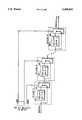
- FIGUREis a block diagram showing the structure of the present invention and how it is controlled by delay selection signals.
- STAGE 1includes a delay element 10 and a multiplexer 12.
- Delay element 10provides a delay equal to 2 N-1 t, where N is the number of stages in the overall programmable variable delay circuit and t is the delay produced by the delay element of the stage with the shortest delay.
- the multiplexer 12selects between the output of the delay element 10 on its "1" input and the input to delay element 10 on its "0" input. The selection made by multiplexer 12 is determined by the most significant bit of N-bits of DELAY SELECT signals.
- the output of STAGE 1is applied to the input of STAGE 2, which has a delay element 20 and a multiplexer 22 that are arranged in the same way that the corresponding circuit elements were arranged in STAGE 1.
- the delay element 20produces a delay equal to 2 N-2 t, or one half of the delay provided by the delay element 10 of the preceding stage.
- the multiplexer 22 in this stageis controlled by the second most significant bit of the N-bits of DELAY SELECT signals.
- successive stages of the programmable variable delay circuit of the present inventionare identical to those already described, except that each succeeding delay element has a delay value that is one half of that of the preceding one and each multiplexer is controlled by a progressively less significant bit of the DELAY SELECT signals. This pattern is repeated until the final stage, STAGE N, is reached.
- the output of STAGE Nis SIGNAL Td , where Td is the delay time of the overall programmable variable delay circuit.
Landscapes
- Physics & Mathematics (AREA)
- Nonlinear Science (AREA)
- Pulse Circuits (AREA)
Abstract
Description
This invention relates to variable length delay circuits for use in electronic design, and more particularly to programmable variable length delay circuits having a simplified structure to conserve parts and to provide ease of programmability.
In electronic design, there is a recurring need for variable length delay circuits whose delay value is programmable during circuit operation.
U.S. Pat. No. 4,016,511 to Ramsey et al. for a "Programmable Variable Length High Speed Digital Delay Line", hereby incorporated by reference, discloses a delay line apparatus that utilizes a set of progressively increasing delay stages in conjunction with a set of digitally selectable switching units. The progressively increasing delay element stages have delay times that are related as powers of two, i.e., 1, 2, 4, . . . , 2N-2, 2N-1. These N delay element stages are arranged in series, connected by N switches that allow the input of any element to be connected to the output of any preceding element or the input to the overall delay line. Each switch must have as many positions as the number of delay element stages in front of it plus one. Thus, for N delay element stages, N switches are required, with those switches having 2, 3, . . .. N, N+1 inputs, respectively. While these switches permit any combination of delay elements to be connected in series, to control them an N-bit delay length word must be decoded into numerous control lines in order to appropriately control each of the multi-input switches.
It would be highly desirable to have a programmable variable delay element with a simplified structure that both conserves parts and provides for simplified programmability.
In accordance with the present invention there is provided a programmable delay circuit with a simplified structure that both conserves parts and provides for simplified programmability. In this structure, N delay stages produce delays that have delay times that are related as powers of two, as in the patent to Ramsey et al. , but in the present invention these delay elements are connected by two-input multiplexers, rather than by multi-input selectors. These two-input multiplexers select between the input and output of the delay element in their stage, and are collectively controlled by N-bits of delay selection signals that are connected so that less significant bits control multiplexers associated with delay elements producing shorter delays and more significant bits control multiplexers associated with delay elements producing longer delays in a monotonic correspondence. The resulting structure conserves parts and produces a delay time that is directly proportional to the binary value used to control the multiplexers.
The drawing FIGURE is a block diagram showing the structure of the present invention and how it is controlled by delay selection signals.
Referring to the FIGURE, a SIGNAL to be delayed is applied to the input of a first stage,STAGE 1.STAGE 1 includes adelay element 10 and amultiplexer 12.Delay element 10 provides a delay equal to 2N-1 t, where N is the number of stages in the overall programmable variable delay circuit and t is the delay produced by the delay element of the stage with the shortest delay. Themultiplexer 12 selects between the output of thedelay element 10 on its "1" input and the input to delayelement 10 on its "0" input. The selection made bymultiplexer 12 is determined by the most significant bit of N-bits of DELAY SELECT signals.
The output ofSTAGE 1 is applied to the input ofSTAGE 2, which has adelay element 20 and amultiplexer 22 that are arranged in the same way that the corresponding circuit elements were arranged inSTAGE 1. Thedelay element 20 produces a delay equal to 2N-2 t, or one half of the delay provided by thedelay element 10 of the preceding stage. Themultiplexer 22 in this stage is controlled by the second most significant bit of the N-bits of DELAY SELECT signals.
Successive stages of the programmable variable delay circuit of the present invention are identical to those already described, except that each succeeding delay element has a delay value that is one half of that of the preceding one and each multiplexer is controlled by a progressively less significant bit of the DELAY SELECT signals. This pattern is repeated until the final stage, STAGE N, is reached. STAGE N has a delay element that is simply t (since 2N-N =20 =1), and its multiplexer is controlled by the least significant bit of the DELAY SELECT signals. The output of STAGE N is SIGNALTd, where Td is the delay time of the overall programmable variable delay circuit.
Since the power of two relationship between the N bits of DELAY SELECT signal is mirrored by the power of two relationship between the delays of the N stages of this delay circuit, the total delay produced, Td, is directly proportional to the digital value on the DELAY SELECT signal lines. And, as long as this relationship is preserved, it does not matter what order the different stages are physically connected in; e.g. , reverse order would work equally well, if the relationship between bit significance and stage delay time were preserved.
Thedelay elements
While the foregoing description has described an embodiment based on powers of two, the invention is not necessarily limited to that assuption. Alternative embodiments can be envisioned in which the delays associated with each stage are related as powers of a number other than two, e.g. ten or some other number Y. In this more general embodiment, each successive delay is Y times larger or smaller than the succeeding one; i.e., 1, Y, Y2, . . . YN-2, YN-1, to provide a total delay that is the sum of any set of these values. This embodiment does not, however, provide sums representing all possible delay values nor does it provide direct proportionality between the binary control bit values and the delay selected.
While a preferred embodiment of the present invention has been shown and described, it will be apparent to those skilled in the art that many changes and modifications may be made without departing from the invention in its broader aspects. The claims that follow are therefore intended to cover all such changes and modifications as fall within the true scope and spirit of the invention.
Claims (2)
1. A programmable variable delay circuit comprising a plurality (1-N) of delay stages connected in series, with each delay stage comprising:
a delay element (10,20, . . . ,80) having an input and an output, with the delay element associated with each different delay stage providing a characteristic delay time that is an integral power of a base number Y of a unit characteristic delay time t of a shortest delay element, with each delay stage producing a different delay and the delays associated with the plurality of delay stages including delays corresponding to t times each integral power of Y from 0 to N-1; and
selecting means (12,22, . . . ,82) having two inputs, for selecting as an output of a particular stage either the input or the output of that stage's delay element;
and the programmable variable delay circuit further comprising N-bits of delay selection signals, with the delay selection signals being connected to the selecting means of the plurality of delay stages such that less significant bits are connected to selection means associated with shorter delays and more significant bits are connected to selection means associated with longer delays in a monotonic correspondence, so that digital values applied to the delay selection signals produce proportional cumulative delays from the variable delay circuit.
2. A programmable variable delay circuit comprising a plurality (1-N) of delay stages connected in series, with each delay stage comprising:
a delay element (10,20, . . . ,80) having an input and an output, with the delay element associated with each different delay stage providing a characteristic delay time that is an integral power of two of a unit characteristic delay time t of a shortest delay element, with each delay stage producing a different delay and the delays associated with the plurality of delay stages including delays corresponding to t times each integral power of two from 0 to N-1; and
selecting means (12,22, . . . ,82) having two inputs, for selecting as an output of a particular stage either the input or the output of that stage's delay element, so that by suitable control of the signal selecting means any combination of delays from 0 to (2N -1)*t may be obtained;
and the programmable variable delay circuit further comprising N-bits of delay selection signals, with the delay selection signals being connected to the selecting means of the plurality of delay stages such that less significant bits are connected to selection means associated with shorter delays and more significant bits are connected to selection means associated with longer delays in a monotonic correspondence, so that digital values applied to the delay selection signals produce proportional cumulative delays from the variable delays circuit.
Priority Applications (2)
| Application Number | Priority Date | Filing Date | Title |
|---|---|---|---|
| US07/936,819US5389843A (en) | 1992-08-28 | 1992-08-28 | Simplified structure for programmable delays |
| JP5235432AJPH06196958A (en) | 1992-08-28 | 1993-08-27 | Programmable variable length delay circuit |
Applications Claiming Priority (1)
| Application Number | Priority Date | Filing Date | Title |
|---|---|---|---|
| US07/936,819US5389843A (en) | 1992-08-28 | 1992-08-28 | Simplified structure for programmable delays |
Publications (1)
| Publication Number | Publication Date |
|---|---|
| US5389843Atrue US5389843A (en) | 1995-02-14 |
Family
ID=25469112
Family Applications (1)
| Application Number | Title | Priority Date | Filing Date |
|---|---|---|---|
| US07/936,819Expired - Fee RelatedUS5389843A (en) | 1992-08-28 | 1992-08-28 | Simplified structure for programmable delays |
Country Status (2)
| Country | Link |
|---|---|
| US (1) | US5389843A (en) |
| JP (1) | JPH06196958A (en) |
Cited By (32)
| Publication number | Priority date | Publication date | Assignee | Title |
|---|---|---|---|---|
| US5570294A (en)* | 1994-03-11 | 1996-10-29 | Advanced Micro Devices | Circuit configuration employing a compare unit for testing variably controlled delay units |
| US5646564A (en)* | 1994-09-02 | 1997-07-08 | Xilinx, Inc. | Phase-locked delay loop for clock correction |
| US5670904A (en)* | 1994-09-21 | 1997-09-23 | Sgs-Thomson Microelectronics S.R.L. | Programmable digital delay unit |
| US5801559A (en)* | 1995-09-06 | 1998-09-01 | Mitsubishi Denki Kabushiki Kaisha | Clock generating circuit, PLL circuit, semiconductor device, and methods for designing and making the clock generating circuit |
| US5815016A (en)* | 1994-09-02 | 1998-09-29 | Xilinx, Inc. | Phase-locked delay loop for clock correction |
| US5894548A (en)* | 1994-03-29 | 1999-04-13 | Kabushiki Kaisha Toshiba | Semiconductor device having test circuit |
| US5920216A (en)* | 1997-04-03 | 1999-07-06 | Advanced Micro Devices, Inc. | Method and system for generating digital clock signals of programmable frequency employing programmable delay lines |
| US6115769A (en)* | 1996-06-28 | 2000-09-05 | Lsi Logic Corporation | Method and apparatus for providing precise circuit delays |
| US6130567A (en)* | 1997-04-18 | 2000-10-10 | Nec Corporation | Semiconductor delay circuit having inverter circuits and transfer gates |
| US6184735B1 (en)* | 1998-10-30 | 2001-02-06 | Kabushiki Kaisha Toshiba | Variable delay circuit |
| US6294937B1 (en) | 1999-05-25 | 2001-09-25 | Lsi Logic Corporation | Method and apparatus for self correcting parallel I/O circuitry |
| US6459319B2 (en)* | 2000-05-26 | 2002-10-01 | Fujitsu Limited | Variable delay circuit and semiconductor integrated circuit having the same |
| US6529057B2 (en)* | 2001-04-12 | 2003-03-04 | Sun Microsystems, Inc. | Stretching, shortening, and/or removing a clock cycle |
| US6557066B1 (en) | 1999-05-25 | 2003-04-29 | Lsi Logic Corporation | Method and apparatus for data dependent, dual level output driver |
| US6628157B1 (en)* | 1997-12-12 | 2003-09-30 | Intel Corporation | Variable delay element for use in delay tuning of integrated circuits |
| US6784704B2 (en)* | 2000-06-01 | 2004-08-31 | Fujitsu Limited | Semiconductor integrated circuit having circuit for changing timing of inactivating power-on resetting circuit |
| US20050248414A1 (en)* | 2004-05-06 | 2005-11-10 | Mauro Osvaldella | Delay line for a ring oscillator circuit |
| US7038518B1 (en)* | 2001-08-07 | 2006-05-02 | Altera Corporation | Method and apparatus for adjusting the phase and frequency of a periodic wave |
| US20060273839A1 (en)* | 2005-05-17 | 2006-12-07 | Young-Chul Cho | Delay circuit and semiconductor device including same |
| US20090015308A1 (en)* | 2006-10-13 | 2009-01-15 | Altera Corporation | Efficient delay elements |
| US20090315605A1 (en)* | 2006-08-10 | 2009-12-24 | Panasonic Corporation | Variable delay apparatus |
| US7639054B1 (en)* | 2008-01-16 | 2009-12-29 | Altera Corporation | Techniques for generating programmable delays |
| US7667500B1 (en)* | 2006-11-14 | 2010-02-23 | Xilinx, Inc. | Glitch-suppressor circuits and methods |
| US20100085823A1 (en)* | 2008-10-02 | 2010-04-08 | International Business Machines Corporation | Optimizing Sram Performance over Extended Voltage or Process Range Using Self-Timed Calibration of Local Clock Generator |
| US8004329B1 (en)* | 2010-03-19 | 2011-08-23 | National Semiconductor Corporation | Hardware performance monitor (HPM) with variable resolution for adaptive voltage scaling (AVS) systems |
| US8572426B2 (en) | 2010-05-27 | 2013-10-29 | National Semiconductor Corporation | Hardware performance monitor (HPM) with extended resolution for adaptive voltage scaling (AVS) systems |
| CN106817123A (en)* | 2015-11-27 | 2017-06-09 | 上海贝岭股份有限公司 | Phase compensation device based on digital delay |
| CN108886356A (en)* | 2016-03-10 | 2018-11-23 | 美国亚德诺半导体公司 | Timing generator for generating high-resolution pulses of arbitrary width |
| US20200136412A1 (en)* | 2018-10-31 | 2020-04-30 | Toyota Jidosha Kabushiki Kaisha | Power supply device |
| US11283430B2 (en)* | 2020-06-30 | 2022-03-22 | Fermi Research Alliance, Llc | Gated ring oscillator with constant dynamic power consumption |
| US11635469B2 (en) | 2018-10-31 | 2023-04-25 | Toyota Jidosha Kabushiki Kaisha | Power supply device |
| CN117335776A (en)* | 2023-09-08 | 2024-01-02 | 中国船舶集团有限公司第七〇九研究所 | Programmable delay circuit implementation method based on physical delay unit |
Families Citing this family (1)
| Publication number | Priority date | Publication date | Assignee | Title |
|---|---|---|---|---|
| JP4133814B2 (en) | 2001-07-27 | 2008-08-13 | 株式会社アドバンテスト | Timing generator and semiconductor test apparatus |
Citations (14)
| Publication number | Priority date | Publication date | Assignee | Title |
|---|---|---|---|---|
| US3634772A (en)* | 1971-01-05 | 1972-01-11 | Us Air Force | Digital band-pass detector |
| US3862406A (en)* | 1973-11-12 | 1975-01-21 | Interstate Electronics Corp | Data reordering system |
| US4016511A (en)* | 1975-12-19 | 1977-04-05 | The United States Of America As Represented By The Secretary Of The Air Force | Programmable variable length high speed digital delay line |
| JPS54162945A (en)* | 1978-06-14 | 1979-12-25 | Mitsubishi Electric Corp | Programable delay circuit |
| US4330750A (en)* | 1979-03-13 | 1982-05-18 | International Computers Limited | Variable delay circuits |
| US4458165A (en)* | 1983-03-23 | 1984-07-03 | Tektronix, Inc. | Programmable delay circuit |
| US4626716A (en)* | 1984-04-27 | 1986-12-02 | Sony/Tektronix Corporation | Digital signal delay circuit |
| US4675562A (en)* | 1983-08-01 | 1987-06-23 | Fairchild Semiconductor Corporation | Method and apparatus for dynamically controlling the timing of signals in automatic test systems |
| US4714924A (en)* | 1985-12-30 | 1987-12-22 | Eta Systems, Inc. | Electronic clock tuning system |
| US4820944A (en)* | 1983-08-01 | 1989-04-11 | Schlumberger Systems & Services, Inc. | Method and apparatus for dynamically controlling the timing of signals in automatic test systems |
| US4894626A (en)* | 1988-09-30 | 1990-01-16 | Advanced Micro Devices, Inc. | Variable length shift register |
| US5013944A (en)* | 1989-04-20 | 1991-05-07 | International Business Machines Corporation | Programmable delay line utilizing measured actual delays to provide a highly accurate delay |
| US5055706A (en)* | 1986-10-01 | 1991-10-08 | Kabushiki Kaisha Toshiba | Delay circuit that resets after pulse-like noise |
| US5128555A (en)* | 1991-03-18 | 1992-07-07 | Motorola, Inc. | Pulsed CMOS logic circuit having selectable rise and fall times |
Family Cites Families (1)
| Publication number | Priority date | Publication date | Assignee | Title |
|---|---|---|---|---|
| JPS6193711A (en)* | 1984-10-12 | 1986-05-12 | Nec Ic Microcomput Syst Ltd | Delay circuit |
- 1992
- 1992-08-28USUS07/936,819patent/US5389843A/ennot_activeExpired - Fee Related
- 1993
- 1993-08-27JPJP5235432Apatent/JPH06196958A/enactivePending
Patent Citations (14)
| Publication number | Priority date | Publication date | Assignee | Title |
|---|---|---|---|---|
| US3634772A (en)* | 1971-01-05 | 1972-01-11 | Us Air Force | Digital band-pass detector |
| US3862406A (en)* | 1973-11-12 | 1975-01-21 | Interstate Electronics Corp | Data reordering system |
| US4016511A (en)* | 1975-12-19 | 1977-04-05 | The United States Of America As Represented By The Secretary Of The Air Force | Programmable variable length high speed digital delay line |
| JPS54162945A (en)* | 1978-06-14 | 1979-12-25 | Mitsubishi Electric Corp | Programable delay circuit |
| US4330750A (en)* | 1979-03-13 | 1982-05-18 | International Computers Limited | Variable delay circuits |
| US4458165A (en)* | 1983-03-23 | 1984-07-03 | Tektronix, Inc. | Programmable delay circuit |
| US4820944A (en)* | 1983-08-01 | 1989-04-11 | Schlumberger Systems & Services, Inc. | Method and apparatus for dynamically controlling the timing of signals in automatic test systems |
| US4675562A (en)* | 1983-08-01 | 1987-06-23 | Fairchild Semiconductor Corporation | Method and apparatus for dynamically controlling the timing of signals in automatic test systems |
| US4626716A (en)* | 1984-04-27 | 1986-12-02 | Sony/Tektronix Corporation | Digital signal delay circuit |
| US4714924A (en)* | 1985-12-30 | 1987-12-22 | Eta Systems, Inc. | Electronic clock tuning system |
| US5055706A (en)* | 1986-10-01 | 1991-10-08 | Kabushiki Kaisha Toshiba | Delay circuit that resets after pulse-like noise |
| US4894626A (en)* | 1988-09-30 | 1990-01-16 | Advanced Micro Devices, Inc. | Variable length shift register |
| US5013944A (en)* | 1989-04-20 | 1991-05-07 | International Business Machines Corporation | Programmable delay line utilizing measured actual delays to provide a highly accurate delay |
| US5128555A (en)* | 1991-03-18 | 1992-07-07 | Motorola, Inc. | Pulsed CMOS logic circuit having selectable rise and fall times |
Cited By (46)
| Publication number | Priority date | Publication date | Assignee | Title |
|---|---|---|---|---|
| US5570294A (en)* | 1994-03-11 | 1996-10-29 | Advanced Micro Devices | Circuit configuration employing a compare unit for testing variably controlled delay units |
| US5894548A (en)* | 1994-03-29 | 1999-04-13 | Kabushiki Kaisha Toshiba | Semiconductor device having test circuit |
| US5646564A (en)* | 1994-09-02 | 1997-07-08 | Xilinx, Inc. | Phase-locked delay loop for clock correction |
| US5815016A (en)* | 1994-09-02 | 1998-09-29 | Xilinx, Inc. | Phase-locked delay loop for clock correction |
| US5670904A (en)* | 1994-09-21 | 1997-09-23 | Sgs-Thomson Microelectronics S.R.L. | Programmable digital delay unit |
| US5801559A (en)* | 1995-09-06 | 1998-09-01 | Mitsubishi Denki Kabushiki Kaisha | Clock generating circuit, PLL circuit, semiconductor device, and methods for designing and making the clock generating circuit |
| US6115769A (en)* | 1996-06-28 | 2000-09-05 | Lsi Logic Corporation | Method and apparatus for providing precise circuit delays |
| US5920216A (en)* | 1997-04-03 | 1999-07-06 | Advanced Micro Devices, Inc. | Method and system for generating digital clock signals of programmable frequency employing programmable delay lines |
| US6130567A (en)* | 1997-04-18 | 2000-10-10 | Nec Corporation | Semiconductor delay circuit having inverter circuits and transfer gates |
| US6628157B1 (en)* | 1997-12-12 | 2003-09-30 | Intel Corporation | Variable delay element for use in delay tuning of integrated circuits |
| US6885231B2 (en)* | 1997-12-12 | 2005-04-26 | Intel Corporation | Variable delay element for use in delay tuning of integrated circuits |
| US20050001668A1 (en)* | 1997-12-12 | 2005-01-06 | Ravishankar Kuppuswamy | Variable delay element for use in delay tuning of integrated circuits |
| US6184735B1 (en)* | 1998-10-30 | 2001-02-06 | Kabushiki Kaisha Toshiba | Variable delay circuit |
| US6294937B1 (en) | 1999-05-25 | 2001-09-25 | Lsi Logic Corporation | Method and apparatus for self correcting parallel I/O circuitry |
| US6557066B1 (en) | 1999-05-25 | 2003-04-29 | Lsi Logic Corporation | Method and apparatus for data dependent, dual level output driver |
| US6459319B2 (en)* | 2000-05-26 | 2002-10-01 | Fujitsu Limited | Variable delay circuit and semiconductor integrated circuit having the same |
| US6784704B2 (en)* | 2000-06-01 | 2004-08-31 | Fujitsu Limited | Semiconductor integrated circuit having circuit for changing timing of inactivating power-on resetting circuit |
| US6529057B2 (en)* | 2001-04-12 | 2003-03-04 | Sun Microsystems, Inc. | Stretching, shortening, and/or removing a clock cycle |
| US7038518B1 (en)* | 2001-08-07 | 2006-05-02 | Altera Corporation | Method and apparatus for adjusting the phase and frequency of a periodic wave |
| US20050248414A1 (en)* | 2004-05-06 | 2005-11-10 | Mauro Osvaldella | Delay line for a ring oscillator circuit |
| US7230498B2 (en)* | 2004-05-06 | 2007-06-12 | Stmicroelectronics S.R.L. | Delay line for a ring oscillator circuit |
| US7304520B2 (en)* | 2005-05-17 | 2007-12-04 | Samsung Electronics Co., Ltd. | Delay circuit and semiconductor device including same |
| US20060273839A1 (en)* | 2005-05-17 | 2006-12-07 | Young-Chul Cho | Delay circuit and semiconductor device including same |
| US20090315605A1 (en)* | 2006-08-10 | 2009-12-24 | Panasonic Corporation | Variable delay apparatus |
| US7898312B2 (en)* | 2006-08-10 | 2011-03-01 | Panasonic Corporation | Variable delay apparatus |
| US20090015308A1 (en)* | 2006-10-13 | 2009-01-15 | Altera Corporation | Efficient delay elements |
| US7629825B1 (en)* | 2006-10-13 | 2009-12-08 | Altera Corporation | Efficient delay elements |
| US7659764B2 (en) | 2006-10-13 | 2010-02-09 | Altera Corporation | Efficient delay elements |
| US7667500B1 (en)* | 2006-11-14 | 2010-02-23 | Xilinx, Inc. | Glitch-suppressor circuits and methods |
| US7839181B1 (en) | 2006-11-14 | 2010-11-23 | Xilinx, Inc. | Glitch-suppressor circuits and methods |
| US7639054B1 (en)* | 2008-01-16 | 2009-12-29 | Altera Corporation | Techniques for generating programmable delays |
| US20100085823A1 (en)* | 2008-10-02 | 2010-04-08 | International Business Machines Corporation | Optimizing Sram Performance over Extended Voltage or Process Range Using Self-Timed Calibration of Local Clock Generator |
| US7864625B2 (en) | 2008-10-02 | 2011-01-04 | International Business Machines Corporation | Optimizing SRAM performance over extended voltage or process range using self-timed calibration of local clock generator |
| US8004329B1 (en)* | 2010-03-19 | 2011-08-23 | National Semiconductor Corporation | Hardware performance monitor (HPM) with variable resolution for adaptive voltage scaling (AVS) systems |
| US8572426B2 (en) | 2010-05-27 | 2013-10-29 | National Semiconductor Corporation | Hardware performance monitor (HPM) with extended resolution for adaptive voltage scaling (AVS) systems |
| CN106817123A (en)* | 2015-11-27 | 2017-06-09 | 上海贝岭股份有限公司 | Phase compensation device based on digital delay |
| CN106817123B (en)* | 2015-11-27 | 2021-12-17 | 上海贝岭股份有限公司 | Phase compensation device based on digital time delay |
| CN108886356A (en)* | 2016-03-10 | 2018-11-23 | 美国亚德诺半导体公司 | Timing generator for generating high-resolution pulses of arbitrary width |
| EP3427381A4 (en)* | 2016-03-10 | 2019-11-20 | Analog Devices, Inc. | TIMER GENERATOR FOR GENERATING HIGH RESOLUTION PULSES WITH ARBITRARY WIDTHS |
| CN108886356B (en)* | 2016-03-10 | 2022-03-29 | 美国亚德诺半导体公司 | Timing generator for generating high resolution pulses with arbitrary width |
| US20200136412A1 (en)* | 2018-10-31 | 2020-04-30 | Toyota Jidosha Kabushiki Kaisha | Power supply device |
| US11635469B2 (en) | 2018-10-31 | 2023-04-25 | Toyota Jidosha Kabushiki Kaisha | Power supply device |
| US11757291B2 (en)* | 2018-10-31 | 2023-09-12 | Toyota Jidosha Kabushiki Kaisha | Power supply device |
| US11283430B2 (en)* | 2020-06-30 | 2022-03-22 | Fermi Research Alliance, Llc | Gated ring oscillator with constant dynamic power consumption |
| US11764761B2 (en) | 2020-06-30 | 2023-09-19 | Fermi Research Alliance, Llc | Gated ring oscillator with constant dynamic power consumption |
| CN117335776A (en)* | 2023-09-08 | 2024-01-02 | 中国船舶集团有限公司第七〇九研究所 | Programmable delay circuit implementation method based on physical delay unit |
Also Published As
| Publication number | Publication date |
|---|---|
| JPH06196958A (en) | 1994-07-15 |
Similar Documents
| Publication | Publication Date | Title |
|---|---|---|
| US5389843A (en) | Simplified structure for programmable delays | |
| US5338983A (en) | Application specific exclusive of based logic module architecture for FPGAs | |
| US6025744A (en) | Glitch free delay line multiplexing technique | |
| EP0703663B1 (en) | Programmable digital delay unit | |
| US5448186A (en) | Field-programmable gate array | |
| US4016511A (en) | Programmable variable length high speed digital delay line | |
| US4468607A (en) | Ladder-type signal attenuator | |
| US4573137A (en) | Adder circuit | |
| EP1684434A1 (en) | Thermometer coding circuitry | |
| US6034546A (en) | High performance product term based carry chain scheme | |
| US4530107A (en) | Shift register delay circuit | |
| US5448185A (en) | Programmable dedicated FPGA functional blocks for multiple wide-input functions | |
| US5721809A (en) | Maximum value selector | |
| US5465222A (en) | Barrel shifter or multiply/divide IC structure | |
| US3781822A (en) | Data rate-changing and reordering circuits | |
| US4325129A (en) | Non-linear logic module for increasing complexity of bit sequences | |
| US5923199A (en) | Delay circuit for giving delays of variable width | |
| US6738792B1 (en) | Parallel mask generator | |
| US4956802A (en) | Method and apparatus for a parallel carry generation adder | |
| US5812437A (en) | Programmable logic unit for arithmetic, logic and equality functions | |
| US4411009A (en) | Digital dual half word or single word position scaler | |
| JP2838924B2 (en) | Partial multiplier selection circuit | |
| US20040024805A1 (en) | Adjustment device with shift amount control circuit | |
| JPH04292018A (en) | Variable crc generation circuit | |
| JP2833885B2 (en) | PN code generation circuit |
Legal Events
| Date | Code | Title | Description |
|---|---|---|---|
| AS | Assignment | Owner name:TEKTRONIX, INC., OREGON Free format text:ASSIGNMENT OF ASSIGNORS INTEREST;ASSIGNOR:MC KINNEY, DAVID J.;REEL/FRAME:007170/0564 Effective date:19920828 | |
| REMI | Maintenance fee reminder mailed | ||
| LAPS | Lapse for failure to pay maintenance fees | ||
| FP | Lapsed due to failure to pay maintenance fee | Effective date:19990214 | |
| STCH | Information on status: patent discontinuation | Free format text:PATENT EXPIRED DUE TO NONPAYMENT OF MAINTENANCE FEES UNDER 37 CFR 1.362 |