US5389571A - Method of fabricating a gallium nitride based semiconductor device with an aluminum and nitrogen containing intermediate layer - Google Patents
Method of fabricating a gallium nitride based semiconductor device with an aluminum and nitrogen containing intermediate layerDownload PDFInfo
- Publication number
- US5389571A US5389571AUS08/046,960US4696093AUS5389571AUS 5389571 AUS5389571 AUS 5389571AUS 4696093 AUS4696093 AUS 4696093AUS 5389571 AUS5389571 AUS 5389571A
- Authority
- US
- United States
- Prior art keywords
- substrate
- intermediate layer
- single crystal
- layer
- semiconductor device
- Prior art date
- Legal status (The legal status is an assumption and is not a legal conclusion. Google has not performed a legal analysis and makes no representation as to the accuracy of the status listed.)
- Expired - Lifetime
Links
- JMASRVWKEDWRBT-UHFFFAOYSA-NGallium nitrideChemical compound[Ga]#NJMASRVWKEDWRBT-UHFFFAOYSA-N0.000titleclaimsabstractdescription74
- 229910002601GaNInorganic materials0.000titleclaimsabstractdescription73
- 239000004065semiconductorSubstances0.000titleclaimsabstractdescription29
- 229910052782aluminiumInorganic materials0.000titleclaimsabstractdescription15
- 238000004519manufacturing processMethods0.000titleclaimsabstractdescription14
- XAGFODPZIPBFFR-UHFFFAOYSA-NaluminiumChemical compound[Al]XAGFODPZIPBFFR-UHFFFAOYSA-N0.000titleclaimsabstractdescription11
- QJGQUHMNIGDVPM-UHFFFAOYSA-Nnitrogen groupChemical group[N]QJGQUHMNIGDVPM-UHFFFAOYSA-N0.000title1
- 239000013078crystalSubstances0.000claimsabstractdescription87
- 239000000758substrateSubstances0.000claimsabstractdescription85
- IJGRMHOSHXDMSA-UHFFFAOYSA-NAtomic nitrogenChemical compoundN#NIJGRMHOSHXDMSA-UHFFFAOYSA-N0.000claimsabstractdescription14
- XUIMIQQOPSSXEZ-UHFFFAOYSA-NSiliconChemical compound[Si]XUIMIQQOPSSXEZ-UHFFFAOYSA-N0.000claimsabstractdescription11
- 229910052710siliconInorganic materials0.000claimsabstractdescription11
- 239000010703siliconSubstances0.000claimsabstractdescription11
- 150000001875compoundsChemical class0.000claimsabstractdescription10
- 229910052757nitrogenInorganic materials0.000claimsabstractdescription10
- -1nitrogen-containing compoundChemical class0.000claimsabstractdescription4
- 238000000034methodMethods0.000claimsdescription23
- 239000010409thin filmSubstances0.000claimsdescription6
- 230000007547defectEffects0.000abstractdescription3
- 238000002425crystallisationMethods0.000abstract1
- 230000008025crystallizationEffects0.000abstract1
- 229910052594sapphireInorganic materials0.000description8
- 239000010980sapphireSubstances0.000description8
- 239000012535impuritySubstances0.000description6
- VYPSYNLAJGMNEJ-UHFFFAOYSA-Nsilicon dioxideInorganic materialsO=[Si]=OVYPSYNLAJGMNEJ-UHFFFAOYSA-N0.000description6
- QGZKDVFQNNGYKY-UHFFFAOYSA-NAmmoniaChemical compoundNQGZKDVFQNNGYKY-UHFFFAOYSA-N0.000description5
- 238000010894electron beam technologyMethods0.000description5
- 229910015367Au—SbInorganic materials0.000description4
- 230000000052comparative effectEffects0.000description4
- 239000010408filmSubstances0.000description4
- 239000000463materialSubstances0.000description4
- 150000002736metal compoundsChemical class0.000description4
- 239000000203mixtureSubstances0.000description4
- 150000002902organometallic compoundsChemical class0.000description4
- JLTRXTDYQLMHGR-UHFFFAOYSA-NtrimethylaluminiumChemical compoundC[Al](C)CJLTRXTDYQLMHGR-UHFFFAOYSA-N0.000description4
- XCZXGTMEAKBVPV-UHFFFAOYSA-NtrimethylgalliumChemical compoundC[Ga](C)CXCZXGTMEAKBVPV-UHFFFAOYSA-N0.000description4
- OKKJLVBELUTLKV-UHFFFAOYSA-NMethanolChemical compoundOCOKKJLVBELUTLKV-UHFFFAOYSA-N0.000description3
- 230000000694effectsEffects0.000description3
- 238000002474experimental methodMethods0.000description3
- 239000007789gasSubstances0.000description3
- 238000002844meltingMethods0.000description3
- 230000008018meltingEffects0.000description3
- 229910017464nitrogen compoundInorganic materials0.000description3
- 150000002830nitrogen compoundsChemical class0.000description3
- 239000002994raw materialSubstances0.000description3
- IBEFSUTVZWZJEL-UHFFFAOYSA-NtrimethylindiumChemical compoundC[In](C)CIBEFSUTVZWZJEL-UHFFFAOYSA-N0.000description3
- 230000005428wave functionEffects0.000description3
- 229910002704AlGaNInorganic materials0.000description2
- KRHYYFGTRYWZRS-UHFFFAOYSA-NFluoraneChemical compoundFKRHYYFGTRYWZRS-UHFFFAOYSA-N0.000description2
- UFHFLCQGNIYNRP-UHFFFAOYSA-NHydrogenChemical compound[H][H]UFHFLCQGNIYNRP-UHFFFAOYSA-N0.000description2
- 238000002441X-ray diffractionMethods0.000description2
- 230000015572biosynthetic processEffects0.000description2
- 229910052681coesiteInorganic materials0.000description2
- 229910052906cristobaliteInorganic materials0.000description2
- 238000005516engineering processMethods0.000description2
- 229910052733galliumInorganic materials0.000description2
- 239000001257hydrogenSubstances0.000description2
- 229910052739hydrogenInorganic materials0.000description2
- 229910052751metalInorganic materials0.000description2
- 239000002184metalSubstances0.000description2
- 239000010453quartzSubstances0.000description2
- 239000000377silicon dioxideSubstances0.000description2
- 229910052682stishoviteInorganic materials0.000description2
- 229910052905tridymiteInorganic materials0.000description2
- 239000012808vapor phaseSubstances0.000description2
- RYGMFSIKBFXOCR-UHFFFAOYSA-NCopperChemical compound[Cu]RYGMFSIKBFXOCR-UHFFFAOYSA-N0.000description1
- GYHNNYVSQQEPJS-UHFFFAOYSA-NGalliumChemical compound[Ga]GYHNNYVSQQEPJS-UHFFFAOYSA-N0.000description1
- FYYHWMGAXLPEAU-UHFFFAOYSA-NMagnesiumChemical compound[Mg]FYYHWMGAXLPEAU-UHFFFAOYSA-N0.000description1
- 229910018540Si CInorganic materials0.000description1
- HCHKCACWOHOZIP-UHFFFAOYSA-NZincChemical compound[Zn]HCHKCACWOHOZIP-UHFFFAOYSA-N0.000description1
- 229910021529ammoniaInorganic materials0.000description1
- 229910052802copperInorganic materials0.000description1
- 239000010949copperSubstances0.000description1
- 238000000354decomposition reactionMethods0.000description1
- 238000000151depositionMethods0.000description1
- 125000005842heteroatomChemical group0.000description1
- 229910052738indiumInorganic materials0.000description1
- 238000002347injectionMethods0.000description1
- 239000007924injectionSubstances0.000description1
- 239000011810insulating materialSubstances0.000description1
- 238000000344low-energy electron-beam lithographyMethods0.000description1
- 229910052749magnesiumInorganic materials0.000description1
- 239000011777magnesiumSubstances0.000description1
- 150000004767nitridesChemical class0.000description1
- 239000003960organic solventSubstances0.000description1
- 238000000926separation methodMethods0.000description1
- 238000004467single crystal X-ray diffractionMethods0.000description1
- 239000007787solidSubstances0.000description1
- 230000001052transient effectEffects0.000description1
- 238000000927vapour-phase epitaxyMethods0.000description1
- XLYOFNOQVPJJNP-UHFFFAOYSA-NwaterSubstancesOXLYOFNOQVPJJNP-UHFFFAOYSA-N0.000description1
- 229910052725zincInorganic materials0.000description1
- 239000011701zincSubstances0.000description1
Images


Classifications
- H—ELECTRICITY
- H10—SEMICONDUCTOR DEVICES; ELECTRIC SOLID-STATE DEVICES NOT OTHERWISE PROVIDED FOR
- H10H—INORGANIC LIGHT-EMITTING SEMICONDUCTOR DEVICES HAVING POTENTIAL BARRIERS
- H10H20/00—Individual inorganic light-emitting semiconductor devices having potential barriers, e.g. light-emitting diodes [LED]
- H10H20/80—Constructional details
- H10H20/81—Bodies
- H10H20/822—Materials of the light-emitting regions
- H10H20/824—Materials of the light-emitting regions comprising only Group III-V materials, e.g. GaP
- H10H20/825—Materials of the light-emitting regions comprising only Group III-V materials, e.g. GaP containing nitrogen, e.g. GaN
- H—ELECTRICITY
- H01—ELECTRIC ELEMENTS
- H01L—SEMICONDUCTOR DEVICES NOT COVERED BY CLASS H10
- H01L21/00—Processes or apparatus adapted for the manufacture or treatment of semiconductor or solid state devices or of parts thereof
- H01L21/02—Manufacture or treatment of semiconductor devices or of parts thereof
- H01L21/02104—Forming layers
- H01L21/02365—Forming inorganic semiconducting materials on a substrate
- H01L21/02367—Substrates
- H01L21/0237—Materials
- H01L21/02373—Group 14 semiconducting materials
- H01L21/02381—Silicon, silicon germanium, germanium
- H—ELECTRICITY
- H01—ELECTRIC ELEMENTS
- H01L—SEMICONDUCTOR DEVICES NOT COVERED BY CLASS H10
- H01L21/00—Processes or apparatus adapted for the manufacture or treatment of semiconductor or solid state devices or of parts thereof
- H01L21/02—Manufacture or treatment of semiconductor devices or of parts thereof
- H01L21/02104—Forming layers
- H01L21/02365—Forming inorganic semiconducting materials on a substrate
- H01L21/02436—Intermediate layers between substrates and deposited layers
- H01L21/02439—Materials
- H01L21/02455—Group 13/15 materials
- H01L21/02458—Nitrides
- H—ELECTRICITY
- H01—ELECTRIC ELEMENTS
- H01L—SEMICONDUCTOR DEVICES NOT COVERED BY CLASS H10
- H01L21/00—Processes or apparatus adapted for the manufacture or treatment of semiconductor or solid state devices or of parts thereof
- H01L21/02—Manufacture or treatment of semiconductor devices or of parts thereof
- H01L21/02104—Forming layers
- H01L21/02365—Forming inorganic semiconducting materials on a substrate
- H01L21/02518—Deposited layers
- H01L21/02521—Materials
- H01L21/02538—Group 13/15 materials
- H01L21/0254—Nitrides
- H—ELECTRICITY
- H01—ELECTRIC ELEMENTS
- H01L—SEMICONDUCTOR DEVICES NOT COVERED BY CLASS H10
- H01L21/00—Processes or apparatus adapted for the manufacture or treatment of semiconductor or solid state devices or of parts thereof
- H01L21/02—Manufacture or treatment of semiconductor devices or of parts thereof
- H01L21/02104—Forming layers
- H01L21/02365—Forming inorganic semiconducting materials on a substrate
- H01L21/02612—Formation types
- H01L21/02617—Deposition types
- H01L21/0262—Reduction or decomposition of gaseous compounds, e.g. CVD
- H—ELECTRICITY
- H01—ELECTRIC ELEMENTS
- H01L—SEMICONDUCTOR DEVICES NOT COVERED BY CLASS H10
- H01L21/00—Processes or apparatus adapted for the manufacture or treatment of semiconductor or solid state devices or of parts thereof
- H01L21/02—Manufacture or treatment of semiconductor devices or of parts thereof
- H01L21/02104—Forming layers
- H01L21/02365—Forming inorganic semiconducting materials on a substrate
- H01L21/02612—Formation types
- H01L21/02617—Deposition types
- H01L21/02636—Selective deposition, e.g. simultaneous growth of mono- and non-monocrystalline semiconductor materials
- H01L21/02639—Preparation of substrate for selective deposition
- H—ELECTRICITY
- H01—ELECTRIC ELEMENTS
- H01L—SEMICONDUCTOR DEVICES NOT COVERED BY CLASS H10
- H01L21/00—Processes or apparatus adapted for the manufacture or treatment of semiconductor or solid state devices or of parts thereof
- H01L21/02—Manufacture or treatment of semiconductor devices or of parts thereof
- H01L21/02104—Forming layers
- H01L21/02365—Forming inorganic semiconducting materials on a substrate
- H01L21/02612—Formation types
- H01L21/02617—Deposition types
- H01L21/02636—Selective deposition, e.g. simultaneous growth of mono- and non-monocrystalline semiconductor materials
- H01L21/02647—Lateral overgrowth
- H—ELECTRICITY
- H10—SEMICONDUCTOR DEVICES; ELECTRIC SOLID-STATE DEVICES NOT OTHERWISE PROVIDED FOR
- H10D—INORGANIC ELECTRIC SEMICONDUCTOR DEVICES
- H10D62/00—Semiconductor bodies, or regions thereof, of devices having potential barriers
- H10D62/80—Semiconductor bodies, or regions thereof, of devices having potential barriers characterised by the materials
- H10D62/85—Semiconductor bodies, or regions thereof, of devices having potential barriers characterised by the materials being Group III-V materials, e.g. GaAs
- H10D62/852—Semiconductor bodies, or regions thereof, of devices having potential barriers characterised by the materials being Group III-V materials, e.g. GaAs being Group III-V materials comprising three or more elements, e.g. AlGaN or InAsSbP
- H—ELECTRICITY
- H10—SEMICONDUCTOR DEVICES; ELECTRIC SOLID-STATE DEVICES NOT OTHERWISE PROVIDED FOR
- H10H—INORGANIC LIGHT-EMITTING SEMICONDUCTOR DEVICES HAVING POTENTIAL BARRIERS
- H10H20/00—Individual inorganic light-emitting semiconductor devices having potential barriers, e.g. light-emitting diodes [LED]
- H10H20/01—Manufacture or treatment
- H10H20/011—Manufacture or treatment of bodies, e.g. forming semiconductor layers
- H10H20/013—Manufacture or treatment of bodies, e.g. forming semiconductor layers having light-emitting regions comprising only Group III-V materials
- H10H20/0133—Manufacture or treatment of bodies, e.g. forming semiconductor layers having light-emitting regions comprising only Group III-V materials with a substrate not being Group III-V materials
- H10H20/01335—Manufacture or treatment of bodies, e.g. forming semiconductor layers having light-emitting regions comprising only Group III-V materials with a substrate not being Group III-V materials the light-emitting regions comprising nitride materials
- H—ELECTRICITY
- H10—SEMICONDUCTOR DEVICES; ELECTRIC SOLID-STATE DEVICES NOT OTHERWISE PROVIDED FOR
- H10D—INORGANIC ELECTRIC SEMICONDUCTOR DEVICES
- H10D62/00—Semiconductor bodies, or regions thereof, of devices having potential barriers
- H10D62/80—Semiconductor bodies, or regions thereof, of devices having potential barriers characterised by the materials
- H10D62/85—Semiconductor bodies, or regions thereof, of devices having potential barriers characterised by the materials being Group III-V materials, e.g. GaAs
- H10D62/8503—Nitride Group III-V materials, e.g. AlN or GaN
- Y—GENERAL TAGGING OF NEW TECHNOLOGICAL DEVELOPMENTS; GENERAL TAGGING OF CROSS-SECTIONAL TECHNOLOGIES SPANNING OVER SEVERAL SECTIONS OF THE IPC; TECHNICAL SUBJECTS COVERED BY FORMER USPC CROSS-REFERENCE ART COLLECTIONS [XRACs] AND DIGESTS
- Y10—TECHNICAL SUBJECTS COVERED BY FORMER USPC
- Y10S—TECHNICAL SUBJECTS COVERED BY FORMER USPC CROSS-REFERENCE ART COLLECTIONS [XRACs] AND DIGESTS
- Y10S148/00—Metal treatment
- Y10S148/065—Gp III-V generic compounds-processing
- Y—GENERAL TAGGING OF NEW TECHNOLOGICAL DEVELOPMENTS; GENERAL TAGGING OF CROSS-SECTIONAL TECHNOLOGIES SPANNING OVER SEVERAL SECTIONS OF THE IPC; TECHNICAL SUBJECTS COVERED BY FORMER USPC CROSS-REFERENCE ART COLLECTIONS [XRACs] AND DIGESTS
- Y10—TECHNICAL SUBJECTS COVERED BY FORMER USPC
- Y10S—TECHNICAL SUBJECTS COVERED BY FORMER USPC CROSS-REFERENCE ART COLLECTIONS [XRACs] AND DIGESTS
- Y10S148/00—Metal treatment
- Y10S148/113—Nitrides of boron or aluminum or gallium
- Y—GENERAL TAGGING OF NEW TECHNOLOGICAL DEVELOPMENTS; GENERAL TAGGING OF CROSS-SECTIONAL TECHNOLOGIES SPANNING OVER SEVERAL SECTIONS OF THE IPC; TECHNICAL SUBJECTS COVERED BY FORMER USPC CROSS-REFERENCE ART COLLECTIONS [XRACs] AND DIGESTS
- Y10—TECHNICAL SUBJECTS COVERED BY FORMER USPC
- Y10S—TECHNICAL SUBJECTS COVERED BY FORMER USPC CROSS-REFERENCE ART COLLECTIONS [XRACs] AND DIGESTS
- Y10S438/00—Semiconductor device manufacturing: process
- Y10S438/933—Germanium or silicon or Ge-Si on III-V
Definitions
- the present inventiongenerally relates to a gallium nitride (GaN) type semiconductor device comprising a (Ga 1-x Al x ) 1-y In y N single crystal, which has been receiving growing attention as a wide gap semiconductor in the industry, and a method of fabricating the same. More particularly, this invention is directed to a method of forming on a silicon (Si) substrate a high-quality (Ga 1-x Al x ) 1-y In y N single crystal, which is expected to be a material for a device for emitting or detecting light with a wavelength of 200 to 700 nm.
- GaNgallium nitride
- the (Ga 1-x Al x ) 1-y In y N crystalcontains nitrogen (N) whose equilibrium vapor pressure is very high near the growth temperature, its bulk crystal cannot be easily produced. At present, therefore, the single crystal is produced through a hetero epitaxial growth where different crystals are used as a substrate.
- the substrateAs the essential requirements for a substrate for producing the (Ga 1-x Al x ) 1-y In y N crystal, it is desirable that the substrate have the following characteristics:
- the substrate which is most frequently used at presentis formed of sapphire that satisfies the conditions (1), (2), (3), (5) and (6).
- sapphireSince the difference between the lattice constant of sapphire and that of (Ga 1-x Al x ) 1-y In y N is 11% or more, however, sapphire is not desirable in view of the condition (4). In addition, because sapphire is an insulating material and is rigid, it is not easy to form a gallium nitride type semiconductor device, particularly, its electrode, it is not suitable for a semiconductor device that operates on a large current supplied.
- Siis one of proposed substrate materials to overcome this shortcoming.
- Sia preferable substrate is obtained with a low resistance and high melting point and having a large and substantially perfect crystal.
- a Si substrateis inexpensive and has a high crystal quality, and large crystallinity. The fine working of the Si substrate are easily accomplished. That is, Si fulfills the conditions (1), (2), (3), (5), (6) and (7).
- the biggest issue in yielding a (Ga 1-x Al x ) 1-y In y N crystal on a Si substrateis that there is a large difference in lattice constant of about 17% between GaN and Si, and thus there is a demand for establishment of the technology to suppress the occurrence of crystal defects due to this difference in lattice constant.
- the temperature of the Si substratebe within a range of 400° to 1300° C. in the case where an Al-containing organic metal compound and a nitrogen compound are introduced into a reactor to form a compound containing at least Al and N, e.g., AlN (hereinafter such a compound is referred to as AlN).
- the present inventorshave completed the present invention based on the results of studies of various methods of treating the Si substrate surface to acquire a high-quality (Ga 1-x Al x ) 1-y In y N single crystal on a Si substrate whose electric characteristics are easily controlled and which has an excellent crystalline quality and is inexpensive, by vapor phase epitaxial method, particularly, by organic metal vapor phase epitaxy.
- the feature of the present inventionlies in that AlN is used as an intermediate layer; the use of AlN as an intermediate layer to grow a (Ga 1-x Al x ) 1-y In y N layer on a Si substrate can yield a single crystal of (Ga 1-x Al x ) 1-y In y N with very high quality and considerably excellent flatness as compared with the one obtained by direct growth of GaN on a Si substrate.
- the present inventioncan provide a single crystal of (Ga 1-x Al x ) 1-y In y N at a low cost. Further, this invention can provide availabilites for fine stractures and a high current injection, thereby obtaing a gallium nitride type semiconductor device, particularly, a semiconductor laser diode.
- the present inventorsalso found that depositing a thin AlN (about 50 nm in thickness) on a sapphire substrate at a low temperature (about 600° C.) as a buffer layer before growing a (Ga 1-x Al x ) 1-y In y N crystal can yield a high-quality (Ga 1-x Al x ) 1-y In y N crystal on the sapphire substrate (see Japanese Unexamined Patent Publication No. 60-256806).
- the present inventorshave succeeded in preparing high-performance blue and ultraviolet LEDs using this technique.
- FIGS. 2A, 2B and 2Care schematic cross-sectional views showing individual layers on a Si substrate formed by a method of fabricating a gallium nitride type semiconductor device according to one example of the present invention
- FIG. 3is a schematic cross-sectional view illustrating the structure of a light-emitting diode as a gallium nitride type semiconductor device according to this example of the present invention
- FIGS. 4A, 4B, 4C and 4Dare schematic cross-sectional views showing individual layers on a Si substrate formed by a method of fabricating a gallium nitride type semiconductor device according to another example of the present invention.
- FIG. 5is a schematic cross-sectional view illustrating the structure of a light-emitting diode as a gallium nitride type semiconductor device according to this example of the present invention
- FIGS. 6A and 6Bare schematic cross-sectional views showing individual layers on a Si substrate formed by a method of fabricating a gallium nitride type base semiconductor device according to a further example of the present invention
- FIG. 7is a schematic cross-sectional view illustrating the structure of a light-emitting diode as a gallium nitride type semiconductor device according to this embodiment of the present invention.
- FIGS. 8A and 8Bare schematic cross-sectional views showing individual layers on a Si substrate formed by a method of fabricating a gallium nitride type semiconductor device according to a still further example of the present invention.
- FIG. 9is a schematic cross-sectional view illustrating the structure of a light-emitting diode as a gallium nitride type semiconductor device according to this example of the present invention.
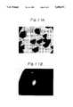
- FIG. 10Ais an enlarged plan view based on a microscopic photograph showing the surface of GaN formed by the present method of fabricating a gallium nitride type semiconductor device, and FIG. 10B shows a diffraction image of reflected electron beams; and
- FIG. 11Ais an enlarged plan view based on a microscopic photograph showing the surface of GaN according to a Comparative Example in the case where GaN is grown directly on a Si substrate, and FIG. 11B shows a diffraction image of reflected electron beams.
- the embodimentemploys a metalorganic compound vapor phase epitaxial method which is excellent in terms of mass production and control of film thickness, and facilitates particularly the fabrication of a light-emitting device.
- a metalorganic compound vapor phase epitaxial methodwhich is excellent in terms of mass production and control of film thickness, and facilitates particularly the fabrication of a light-emitting device.
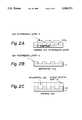
- an AlN thin intermediate layer 2is formed on an n type, low-resistance Si substrate wafer 1 having a (111) plane
- an undoped or Si-doped n type GaN layer 3is grown on the intermediate layer 2.
- an Mg-doped GaN layer 4is selectively grown on the surface of the resultant structure, and then the wafer is removed from a reactor and is subjected to low-energy electron-beam irradiation (Japanese Unexamined Patent Publication No.
- the growing procedureswill be described below. First, after a crystal growing substrate, i.e., a low-resistance Si substrate (a (111) plane was used in the experiment) is cleaned with an organic solvent such as methanol, the oxide on the surface is removed by a hydrofluoric acid type etchant; and the resultant structure is rinsed with pure water and is then placed in a crystal growing section.
- AlN thin filmis formed about 5 to 200 nm in thickness on the Si substrate.
- an Al-containing organic metal compounde.g., trimethyl aluminum (TMA)
- TMAtrimethyl aluminum
- NH 3nitrogen compound such as ammonia
- the substrate temperature at the time of forming the AlN thin filmis lower than 400° C.
- the decomposition of the raw material gasis insufficient so that the advantages of the present invention cannot be expected.
- quartz in the furnacefor the sake of convenience on the apparatus side, no experiment is feasible above 1300° C.
- the AlN buffer layerbecomes thicker than 200 nm, the flatness of the (Ga 1-x Al x ) 1-y In y N layer which grows on the AlN layer becomes lower.
- the substrateis electrically insulated from the GaN layer due to the high resistance of the AlN layer.
- the substratecannot therefore be used as an electrode.
- the AlN intermediate layer 2is formed on the Si substrate 1 which is partially covered with SiO 2 (FIG. 2A), and the resultant structure is temporarily taken out of the furnace to separate SiO 2 . Consequently, the surface of the Si substrate is divided into a portion covered with the AlN layer and a Si-substrate exposed portion (FIG. 2B). In this case, the AlN layer portion and the Si-substrate exposed portion are made to have about the same area. Then, GaN is grown on the resultant substrate. GaN is grown as a single crystal on the AlN intermediate layer 2, yielding a GaN polycrystal on the Si substrate 1.
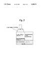
- FIG. 3illustrates the schematic structure of a light-emitting device fabricated by the selective polycrystal yielding technique.
- This light-emitting devicecomprises a Au-Sb electrode, a Si substrate, an AlN intermediate layer, an n type GaN single crystal layer connected via an n type GaN polycrystal layer to the Si substrate, a p type GaN single crystal layer and a Au electrode, laminated one on another in the named order.
- an AlN intermediate layer portion 2 and a Si-substrate exposed portionare formed on the surface of the Si substrate 1 using the same means (FIGS. 4A and 4B) as involved in the selective polycrystal yielding technique (1).
- the area of the AlN intermediate layer portionis made comparatively larger than that of the Si-substrate exposed portion.
- the GaN single crystalis first grown only on the AlN intermediate layer portion (FIG. 4C).
- FIG. 5illustrates the schematic structure of a light-emitting device fabricated by the selective horizontal processing technique.
- This light-emitting devicecomprises a Au-Sb electrode, a Si substrate, an AlN intermediate layer, an n type GaN single crystal layer, a p type GaN single crystal layer and a Au electrode, laminated one on another in the named order.
- an Al x Ga 1-x N (x ⁇ 1) intermediate layer 2is uniformly formed on the Si substrate 1 (FIG. 6A).
- Al x Ga 1-x Ncan be made to have a low resistance by the addition of a donor impurity, it can be electrically connected to the Si substrate 1.
- Siacts as a donor in Al x Ga 1-x N and is automatically doped from the substrate during growth, the Al x Ga 1-x N intermediate layer 2 becomes a low-resistance n type even without intentionally adding an impurity, which is very convenient.
- FIG. 7illustrates the schematic structure of a light-emitting device having the AlGaN intermediate layer.
- This light-emitting devicecomprises a Au-Sb electrode, a Si substrate, an AlGaN intermediate layer, an n type GaN single crystal layer, a p type GaN single crystal layer and a Au electrode, laminated one on another in the named order.
- the AlN intermediate layer 2when the AlN intermediate layer 2 is formed to be a very thin film on the Si substrate 1 (FIG. 8A), the wave function of electrons in the Si substrate of a low-resistance n type, for example, overlaps the wave function of electrons in the n type GaN, causing the flow of a tunnel current, so that GaN is electrically connected to the Si substrate 1.
- the AlN intermediate layer 2should be formed as thin as 10 nm or below, about the same degree as the broadening of the wave function, and it preferably has a thickness of 1 nm or more to effectively serve as an intermediate layer. In this method, the very thin film growing technique is used.
- FIG. 9illustrates the schematic structure of a light-emitting device having the very thin AlN intermediate layer.
- This light-emitting devicecomprises a Au-Sb electrode, a Si substrate, a very thin AlN intermediate layer, an n type GaN single crystal layer, a p type GaN single crystal layer and a Au electrode, laminated one on another in the named order.
- a gallium-containing organic metal compounde.g., trimethyl gallium (TMG)
- TMGtrimethyl gallium
- NH 3trimethyl gallium
- the necessary amounts of TMG, TMA and trimethyl indium (TMI) for a demanded composition of the mixed crystalare supplied.
- the supply of TMG, TMA and TMIis stopped and the temperature is lowered.
- the supply of NH 3is stopped.
- the temperaturelowers approximately to the room temperature, the resultant structure is taken out of the growth apparatus.
- the (Ga 1-x Al x ) 1-y In y N crystal prepared in the above mannershows an n type conductivity without intentionally adding an impurity, it is used directly as an n type layer of the light-emitting device.
- an impurity serving as a donormay be intentionally added at the time of growing the aforementioned (Ga 1-x Al x ) 1-y In y N crystal.
- the amount of the flow of the raw material gasis controlled in such a way that x and y in the entirety or part of the crystal surface take the desired values, while at the same time an impurity as an acceptor, e.g., the gas which is the raw material for zinc or magnesium, is supplied, thereby forming a junction of the (Ga 1-x Al x ) 1-y In y N crystal having different conductivities.
- an impurity as an acceptore.g., the gas which is the raw material for zinc or magnesium
- FIG. 10Apresents a microscopic photograph showing the surface of the GaN crystal grown on the AlN intermediate layer prepared by the present invention
- FIG. 10Bshows a diffraction image of reflected electron beams.
- FIG. 11Apresents a microscopic photograph showing the surface of the GaN crystal directly on the Si substrate as a Comparative Example
- FIG. 11Bshows a diffraction image of reflected electron beams. It is apparent from those photograph that the surface of the GaN crystal prepared using the AlN intermediate layer as in the present invention is significantly flat (FIG. 10A), while the diffraction image of reflected electron beams shows that the acquired GaN is a single crystal with excellent crystallinity as apparent from the Kikuchi lines and Kikuchi band observed in that image (FIG. 10B). With the GaN crystal directly grown on the Si substrate as in the Comparative Example, the crystal simply grows like islands (FIG. 11A), and no diffraction is observed (FIG. 11B), yielding considerably poor crystallinity.
- the individual filmswere evaluated by a single crystal X-ray diffraction evaluating apparatus using the K ⁇ rays of copper as incident X rays.
- the GaN layer prepared by the present inventionshowed strong X-ray diffraction and clear separation of the K ⁇ 1 rays and K ⁇ 2 rays, and had crystallinity by no means inferior to the one grown on the sapphire substrate.
- the film directly formed on the Si substrate of the Comparative Exampleshowed no X-ray diffraction, by which conclusion that this film has poor crystallinity was obtaind.
- the present inventionuses an inexpensive Si substrate, it will be the essential technology particularly in realizing the practical use of a device which emits and receives lights having wavelengths of a visible short wave range and an ultraviolet range.
- a silicon single crystal substrateis kept at a temperature of 400° to 1300° C. and is held in the atmosphere where a metalorganic compound containing at least aluminum and a nitrogen-containing compound are present to form a thin film intermediate layer containing at least aluminum and nitrogen on a part or the entirety of the surface of the single crystal substrate, and then at least one layer or multiple layers of a single crystal of (Ga 1-x Al x ) 1-y In y N are formed on the intermediate layer.
- gallium nitride type semiconductor devicethat has a single crystal of (Ga 1-x Al x ) 1-y In y N, which suppresses the occurrence of crystal defects of the acquired single crystal layer and thus has very high crystallinity and considerably excellent flatness.
Landscapes
- Engineering & Computer Science (AREA)
- Physics & Mathematics (AREA)
- Condensed Matter Physics & Semiconductors (AREA)
- General Physics & Mathematics (AREA)
- Manufacturing & Machinery (AREA)
- Computer Hardware Design (AREA)
- Microelectronics & Electronic Packaging (AREA)
- Power Engineering (AREA)
- Chemical & Material Sciences (AREA)
- Materials Engineering (AREA)
- Led Devices (AREA)
Abstract
Description
This is a divisional of application Ser. No. 07/971,208, filed Nov. 4, 1992, now U.S. Pat. No. 5,239,188.
1. Field of the Invention
The present invention generally relates to a gallium nitride (GaN) type semiconductor device comprising a (Ga1-x Alx)1-y Iny N single crystal, which has been receiving growing attention as a wide gap semiconductor in the industry, and a method of fabricating the same. More particularly, this invention is directed to a method of forming on a silicon (Si) substrate a high-quality (Ga1-x Alx)1-y Iny N single crystal, which is expected to be a material for a device for emitting or detecting light with a wavelength of 200 to 700 nm.
2. Description of the Related Art
A (Ga1-x Alx)1-y Iny N crystal (0≦x≦1, 0≦y≦1, excluding the case of x=1 and y=0) is a direct transient semiconductor with a light wavelength of 200 to 700 nm to the energy band gap at the room temperature, and is expected as a material particularly for a device which emits and receives light having a wavelength of a visible short wavelength range or an ultraviolet range.
Since the (Ga1-x Alx)1-y Iny N crystal contains nitrogen (N) whose equilibrium vapor pressure is very high near the growth temperature, its bulk crystal cannot be easily produced. At present, therefore, the single crystal is produced through a hetero epitaxial growth where different crystals are used as a substrate.
As the essential requirements for a substrate for producing the (Ga1-x Alx)1-y Iny N crystal, it is desirable that the substrate have the following characteristics:
(1) High melting point (at least 1,000° C.)
(2) Chemically stable
(3) Excellent crystal quality
(4) Small difference in lattice constant
(5) Easy to obtain
(6) Large in size
In addition, in the case of fabricating a device which electrically functions:
(7) it is desirable that the electric characteristics be easily controlled; particularly, a low resistance is desirable.
No crystals which satisfy all of those conditions have been found, yet. The substrate which is most frequently used at present is formed of sapphire that satisfies the conditions (1), (2), (3), (5) and (6).
Since the difference between the lattice constant of sapphire and that of (Ga1-x Alx)1-y Iny N is 11% or more, however, sapphire is not desirable in view of the condition (4). In addition, because sapphire is an insulating material and is rigid, it is not easy to form a gallium nitride type semiconductor device, particularly, its electrode, it is not suitable for a semiconductor device that operates on a large current supplied.
Silicon (Si) is one of proposed substrate materials to overcome this shortcoming. By using Si, a preferable substrate is obtained with a low resistance and high melting point and having a large and substantially perfect crystal. A Si substrate is inexpensive and has a high crystal quality, and large crystallinity. The fine working of the Si substrate are easily accomplished. That is, Si fulfills the conditions (1), (2), (3), (5), (6) and (7). The biggest issue in yielding a (Ga1-x Alx)1-y Iny N crystal on a Si substrate is that there is a large difference in lattice constant of about 17% between GaN and Si, and thus there is a demand for establishment of the technology to suppress the occurrence of crystal defects due to this difference in lattice constant.
It is therefore an object of the present invention to provide a gallium nitride type semiconductor device that permits a (Ga1-x Alx)1-y Iny N crystal, which is expected as a material for a device which emits and receives light having a wavelength of a visible short wavelength range or an ultraviolet range, to be formed on a Si substrate, of inexpensive having the above mentioned advantages e.g. high crystal quality, large sign wafer, low cost and well-controlled electrical conductivity.
The present invention is characterized by fabricating a gallium nitride type semiconductor device using a method including a step of, in forming a (Ga1-x Alx)1-y Iny N single crystal on a Si substrate, introducing a metalorganic compound containing at least aluminum (Al) and a nitrogen compound into a reactor before growing the (Ga1-x Alx)1-y Iny N single crystal to form a compound containing at least Al and N, e.g., an AlN thin layer, on a part or entirety of the surface of the Si substrate, then temporarily stopping only the supply of the Al-containing organic metal compound, subsequently supplying metalorganic compounds with necessary amounts of Al, Ga and In corresponding to a desired composition of a mixed crystal, thereby forming a (Ga1-x Alx)1-y Iny N (0≦x≦1, 0≦y≦1, excluding the case of x=1 and y=0) on the thin layer of a compound containing Al and N, i.e., on an intermediate layer.
According to a preferred embodiment of the present invention, it is preferable that the temperature of the Si substrate be within a range of 400° to 1300° C. in the case where an Al-containing organic metal compound and a nitrogen compound are introduced into a reactor to form a compound containing at least Al and N, e.g., AlN (hereinafter such a compound is referred to as AlN).
It is to be noted that the present invention is effective in the case where the AlN molar fraction x of the above mentioned (Ga1-x Alx)1-y Iny N layer ranges from 0 to 1, both 0 and 1 inclusive, and the InN molar fraction y ranges from 0 to 1, both 0 and 1 inclusive, excluding the case of x=1 and y=0.
The present inventors have completed the present invention based on the results of studies of various methods of treating the Si substrate surface to acquire a high-quality (Ga1-x Alx)1-y Iny N single crystal on a Si substrate whose electric characteristics are easily controlled and which has an excellent crystalline quality and is inexpensive, by vapor phase epitaxial method, particularly, by organic metal vapor phase epitaxy.
The biggest difficulty in growing a (Ga1-x Alx)1-y Iny N layer on a Si substrate is a large difference in lattice constant of about 17% between GaN and Si. Actually, even if GaN is allowed to grow directly on a Si substrate, it will be polycrystallized, or it will grow as an island shaped into hexagonal prisms even when it becomes a single crystal. This makes it difficult to yield a high-quality single crystal with good flatness. For instance, T. L. Chu, Journal of Electrochemical Society, Solid State Science, vol. 118, 1971, p. 1200, and Yasuo Morimoto, Kosuke Uchiho and Shintaro Ushio, Journal of Electrochemical Society, vol. 120, 1973, p. 1783 reported the cases of direct growth of GaN on a Si substrate, and the present inventors have re-examined the reports from various aspects only to find that direct growth of a high-quality crystal on a Si substrate is difficult. The present inventors then thought that an intermediate layer might be necessary and studied on various crystals, selecting 3C-SiC as the first candidate.
With 3C-SiC used as an intermediate layer, it has already been confirmed that a high-quality single crystal of (Ga1-x Alx)1-y Iny N can grow (see Japanese Unexamined Patent Publication No. 2-418003). The present inventors further considered that the similar effects could be expected by using AlN having almost the same lattice constant as 3C-SiC as an intermediate layer. Based on their findings, they made various studies to accomplish the present invention. It is apparent from Table 1 that the difference between the lattice constant of 3C-SiC and that of AlN is (0.94%) significantly smaller than those between Si and 3C-Si C (19.74), and AlN and GaN (2.50).
TABLE 1 ______________________________________ Lattice Constants of Si, SiC and Nitride and Differences in Lattice Constant Lattice Lattice Constant Constant (nm) Difference (%) ______________________________________ Si 0.5430 } 19.74 3C--SiC 0.4358 } 0.94 SiC(111)--AIN(0001) AIN 0.3111 } 2.50 GaN 0.3189 ______________________________________
The feature of the present invention lies in that AlN is used as an intermediate layer; the use of AlN as an intermediate layer to grow a (Ga1-x Alx)1-y Iny N layer on a Si substrate can yield a single crystal of (Ga1-x Alx)1-y Iny N with very high quality and considerably excellent flatness as compared with the one obtained by direct growth of GaN on a Si substrate.
The present invention can provide a single crystal of (Ga1-x Alx)1-y Iny N at a low cost. Further, this invention can provide availabilites for fine stractures and a high current injection, thereby obtaing a gallium nitride type semiconductor device, particularly, a semiconductor laser diode. The present inventors also found that depositing a thin AlN (about 50 nm in thickness) on a sapphire substrate at a low temperature (about 600° C.) as a buffer layer before growing a (Ga1-x Alx)1-y Iny N crystal can yield a high-quality (Ga1-x Alx)1-y Iny N crystal on the sapphire substrate (see Japanese Unexamined Patent Publication No. 60-256806). The present inventors have succeeded in preparing high-performance blue and ultraviolet LEDs using this technique.
FIG. 1 is a schematic cross sectional view illustrating the structure of a light-emitting diode which is a gallium nitride type semiconductor device embodying the present invention and has (Ga1-x Alx)1-y Iny N (0≦x≦1, 0≦y≦1, excluding the case of x=1 and y=0) formed on a Si substrate;
FIGS. 2A, 2B and 2C are schematic cross-sectional views showing individual layers on a Si substrate formed by a method of fabricating a gallium nitride type semiconductor device according to one example of the present invention;
FIG. 3 is a schematic cross-sectional view illustrating the structure of a light-emitting diode as a gallium nitride type semiconductor device according to this example of the present invention;
FIGS. 4A, 4B, 4C and 4D are schematic cross-sectional views showing individual layers on a Si substrate formed by a method of fabricating a gallium nitride type semiconductor device according to another example of the present invention;
FIG. 5 is a schematic cross-sectional view illustrating the structure of a light-emitting diode as a gallium nitride type semiconductor device according to this example of the present invention;
FIGS. 6A and 6B are schematic cross-sectional views showing individual layers on a Si substrate formed by a method of fabricating a gallium nitride type base semiconductor device according to a further example of the present invention;
FIG. 7 is a schematic cross-sectional view illustrating the structure of a light-emitting diode as a gallium nitride type semiconductor device according to this embodiment of the present invention;
FIGS. 8A and 8B are schematic cross-sectional views showing individual layers on a Si substrate formed by a method of fabricating a gallium nitride type semiconductor device according to a still further example of the present invention;
FIG. 9 is a schematic cross-sectional view illustrating the structure of a light-emitting diode as a gallium nitride type semiconductor device according to this example of the present invention;
FIG. 10A is an enlarged plan view based on a microscopic photograph showing the surface of GaN formed by the present method of fabricating a gallium nitride type semiconductor device, and FIG. 10B shows a diffraction image of reflected electron beams; and
FIG. 11A is an enlarged plan view based on a microscopic photograph showing the surface of GaN according to a Comparative Example in the case where GaN is grown directly on a Si substrate, and FIG. 11B shows a diffraction image of reflected electron beams.
A method of forming a single crystal of (Ga1-x Alx)1-y Iny N (0≦x≦1, 0≦y≦1, excluding the case of x=1 and y=0) on a Si substrate according to a preferred embodiment of the present invention will now be described. It is to be noted that the embodiment and examples to be described below simply illustrates the invention, and the invention is not limited thereto.
The embodiment employs a metalorganic compound vapor phase epitaxial method which is excellent in terms of mass production and control of film thickness, and facilitates particularly the fabrication of a light-emitting device. As illustrated in FIG. 1, after an AlN thinintermediate layer 2 is formed on an n type, low-resistanceSi substrate wafer 1 having a (111) plane, an undoped or Si-doped ntype GaN layer 3 is grown on theintermediate layer 2. Next, an Mg-dopedGaN layer 4 is selectively grown on the surface of the resultant structure, and then the wafer is removed from a reactor and is subjected to low-energy electron-beam irradiation (Japanese Unexamined Patent Publication No. 2-2614) to partially transform the Mg-dopedGaN layer 4 to a p type, forminga p type region 5. Then,metal electrodes type GaN layer 3 and the ptype GaN region 5, respectively, and leads 7A and 7B are connected to therespective electrodes type GaN layer 3 as the negative side and the Mg-doped ptype GaN region 5 as the positive side, blue and ultraviolet lights were emitted at a voltage of around 3.5 V at the room temperature.
The AlN intermediate layer and a single crystal of (Ga1-x Alx)1-y Iny N (0≦x≦1, 0≦y≦1, excluding the case of x=1 and y=0) were formed using the ordinary horizontal type compound semiconductor crystal growth apparatus. The growing procedures will be described below. First, after a crystal growing substrate, i.e., a low-resistance Si substrate (a (111) plane was used in the experiment) is cleaned with an organic solvent such as methanol, the oxide on the surface is removed by a hydrofluoric acid type etchant; and the resultant structure is rinsed with pure water and is then placed in a crystal growing section. After the furnace is evacuated, hydrogen is supplied there and the temperature is raised to, for example, about 1200° C. (in the range of 400° to 1300° C.). Since this growth apparatus uses quartz in the furnace, whose melting point is 1300° C., the experiment above that temperature is difficult and has not been conducted.
Hydrogen is added into the furnace thereafter, and an Al-containing organic metal compound, e.g., trimethyl aluminum (TMA), and a nitrogen compound such as ammonia (NH3) are introduced into the growth apparatus, forming an AlN thin film about 5 to 200 nm in thickness on the Si substrate. When the substrate temperature at the time of forming the AlN thin film is lower than 400° C., the decomposition of the raw material gas is insufficient so that the advantages of the present invention cannot be expected. Due to the use of quartz in the furnace for the sake of convenience on the apparatus side, no experiment is feasible above 1300° C. In addition, if the AlN buffer layer becomes thicker than 200 nm, the flatness of the (Ga1-x Alx)1-y Iny N layer which grows on the AlN layer becomes lower.
While the use of the AlN intermediate layer is effective in providing a high-quality GaN single crystal, for example, on the Si substrate, the substrate is electrically insulated from the GaN layer due to the high resistance of the AlN layer. The substrate cannot therefore be used as an electrode. There are many ways to overcome this problem, and four of them will be discussed below.
(i) Use of Selective Polycrystal Yielding Technique
As schematically illustrated in the growing process in FIG. 2, the AlNintermediate layer 2 is formed on theSi substrate 1 which is partially covered with SiO2 (FIG. 2A), and the resultant structure is temporarily taken out of the furnace to separate SiO2. Consequently, the surface of the Si substrate is divided into a portion covered with the AlN layer and a Si-substrate exposed portion (FIG. 2B). In this case, the AlN layer portion and the Si-substrate exposed portion are made to have about the same area. Then, GaN is grown on the resultant substrate. GaN is grown as a single crystal on the AlNintermediate layer 2, yielding a GaN polycrystal on theSi substrate 1. The GaN polycrystal on theSi substrate 1 shows a low-resistance n type conductivity and will not have a high resistance even when an acceptor impurity is added, so that the Si substrate and the GaN single crystal are electrically connected together via the GaN polycrystal (FIG. 2C). FIG. 3 illustrates the schematic structure of a light-emitting device fabricated by the selective polycrystal yielding technique. This light-emitting device comprises a Au-Sb electrode, a Si substrate, an AlN intermediate layer, an n type GaN single crystal layer connected via an n type GaN polycrystal layer to the Si substrate, a p type GaN single crystal layer and a Au electrode, laminated one on another in the named order.
(ii) Use of Selective Horizontal Processing Technique
As schematically illustrated in the growing process in FIGS. 4A, 4B, 4C and 4D, an AlNintermediate layer portion 2 and a Si-substrate exposed portion are formed on the surface of theSi substrate 1 using the same means (FIGS. 4A and 4B) as involved in the selective polycrystal yielding technique (1). In this case, the area of the AlN intermediate layer portion is made comparatively larger than that of the Si-substrate exposed portion. As a GaN single crystal is grown on the resultant substrate, the GaN single crystal is first grown only on the AlN intermediate layer portion (FIG. 4C). The GaN single crystal grown on the AlN intermediate layer then grows horizontally to be coupled to the GaN layer which has grown on the adjoining AlN intermediate layer, and finally, one GaN single crystal is yielded on the whole Si substrate 1 (FIG. 4D). The Si substrate and the GaN single crystal are electrically connected together at the horizontally-grown portion. FIG. 5 illustrates the schematic structure of a light-emitting device fabricated by the selective horizontal processing technique. This light-emitting device comprises a Au-Sb electrode, a Si substrate, an AlN intermediate layer, an n type GaN single crystal layer, a p type GaN single crystal layer and a Au electrode, laminated one on another in the named order.
(iii) Use of Alx Ga1-x N (x≠1) Intermediate Layer
As schematically illustrated in the growing process in FIGS. 6A and 6B, instead of the AlN intermediate layer, an Alx Ga1-x N (x≠1)intermediate layer 2 is uniformly formed on the Si substrate 1 (FIG. 6A). As Alx Ga1-x N can be made to have a low resistance by the addition of a donor impurity, it can be electrically connected to theSi substrate 1. Actually, since Si acts as a donor in Alx Ga1-x N and is automatically doped from the substrate during growth, the Alx Ga1-x Nintermediate layer 2 becomes a low-resistance n type even without intentionally adding an impurity, which is very convenient. With regard to the composition of a mixed crystal, it is preferable that x is equal to or above 0.1, in which case the Alx Ga1-x Nintermediate layer 2 produces about the same effect as the aforementioned AlN intermediate layer. A GaN single crystal is grown on this intermediate layer 2 (FIG. 6B). FIG. 7 illustrates the schematic structure of a light-emitting device having the AlGaN intermediate layer. This light-emitting device comprises a Au-Sb electrode, a Si substrate, an AlGaN intermediate layer, an n type GaN single crystal layer, a p type GaN single crystal layer and a Au electrode, laminated one on another in the named order.
(iv) Use of Very Thin AlN Intermediate Layer
As schematically illustrated in the growing process in FIGS. 8A and 8B, when the AlNintermediate layer 2 is formed to be a very thin film on the Si substrate 1 (FIG. 8A), the wave function of electrons in the Si substrate of a low-resistance n type, for example, overlaps the wave function of electrons in the n type GaN, causing the flow of a tunnel current, so that GaN is electrically connected to theSi substrate 1. To utilize this effect, the AlNintermediate layer 2 should be formed as thin as 10 nm or below, about the same degree as the broadening of the wave function, and it preferably has a thickness of 1 nm or more to effectively serve as an intermediate layer. In this method, the very thin film growing technique is used. A GaN single crystal is grown on this intermediate layer 2 (FIG. 8B). FIG. 9 illustrates the schematic structure of a light-emitting device having the very thin AlN intermediate layer. This light-emitting device comprises a Au-Sb electrode, a Si substrate, a very thin AlN intermediate layer, an n type GaN single crystal layer, a p type GaN single crystal layer and a Au electrode, laminated one on another in the named order.
The above completes the process of forming the intermediate layer.
After the process for forming the intermediate layer, with the substrate temperature set to 1040° C., for example, a gallium-containing organic metal compound, e.g., trimethyl gallium (TMG), and NH3 are supplied into the growth apparatus to grow a GaN layer as in the case of crystal growth on a sapphire substrate. In growing a mixed crystal, the necessary amounts of TMG, TMA and trimethyl indium (TMI) for a demanded composition of the mixed crystal are supplied.
After the thickness of the (Ga1-x Alx)1-y Iny N layer reaches the desired thickness, the supply of TMG, TMA and TMI is stopped and the temperature is lowered. After the substrate temperature becomes 600° C. or below, the supply of NH3 is stopped. When the temperature lowers approximately to the room temperature, the resultant structure is taken out of the growth apparatus. The present invention provides the same advantages in growing the (Ga1-x Alx)1-y Iny N mixed crystal in almost all the compositions of the mixed crystal. It should however be noted that the advantages of the present invention cannot be expected in the case of growing AlN (x=1 and y=0) on the intermediate layer.
Since the (Ga1-x Alx)1-y Iny N crystal prepared in the above manner shows an n type conductivity without intentionally adding an impurity, it is used directly as an n type layer of the light-emitting device. Of course, an impurity serving as a donor may be intentionally added at the time of growing the aforementioned (Ga1-x Alx)1-y Iny N crystal. Next, the amount of the flow of the raw material gas is controlled in such a way that x and y in the entirety or part of the crystal surface take the desired values, while at the same time an impurity as an acceptor, e.g., the gas which is the raw material for zinc or magnesium, is supplied, thereby forming a junction of the (Ga1-x Alx)1-y Iny N crystal having different conductivities. After the growth is complete and the resultant wafer is taken out of the furnace, electrodes are formed on the individual layers having different conductivities, thus completing the fabrication of a light-emitting device.
FIG. 10A presents a microscopic photograph showing the surface of the GaN crystal grown on the AlN intermediate layer prepared by the present invention, and FIG. 10B shows a diffraction image of reflected electron beams.
FIG. 11A presents a microscopic photograph showing the surface of the GaN crystal directly on the Si substrate as a Comparative Example, and FIG. 11B shows a diffraction image of reflected electron beams. It is apparent from those photograph that the surface of the GaN crystal prepared using the AlN intermediate layer as in the present invention is significantly flat (FIG. 10A), while the diffraction image of reflected electron beams shows that the acquired GaN is a single crystal with excellent crystallinity as apparent from the Kikuchi lines and Kikuchi band observed in that image (FIG. 10B). With the GaN crystal directly grown on the Si substrate as in the Comparative Example, the crystal simply grows like islands (FIG. 11A), and no diffraction is observed (FIG. 11B), yielding considerably poor crystallinity.
The individual films were evaluated by a single crystal X-ray diffraction evaluating apparatus using the Kα rays of copper as incident X rays. The GaN layer prepared by the present invention showed strong X-ray diffraction and clear separation of the Kα1 rays and Kα2 rays, and had crystallinity by no means inferior to the one grown on the sapphire substrate. The film directly formed on the Si substrate of the Comparative Example showed no X-ray diffraction, by which conclusion that this film has poor crystallinity was obtaind.
As the present invention uses an inexpensive Si substrate, it will be the essential technology particularly in realizing the practical use of a device which emits and receives lights having wavelengths of a visible short wave range and an ultraviolet range.
As described above, a gallium nitride type semiconductor device embodying the present invention comprises a silicon substrate, an intermediate layer consisting of a compound containing at least aluminum and nitrogen and formed on the silicon substrate, and a crystal layer of (Ga1-x Alx)1-y Iny N (0≦x≦1, 0≦y≦1, excluding the case of x=1 and y=0), so that this semiconductor device can operate even when a large current is supplied and also it can facilitate fine working, particularly, the formation of electrodes.
According to the present method of fabricating a gallium nitride type semiconductor device, a silicon single crystal substrate is kept at a temperature of 400° to 1300° C. and is held in the atmosphere where a metalorganic compound containing at least aluminum and a nitrogen-containing compound are present to form a thin film intermediate layer containing at least aluminum and nitrogen on a part or the entirety of the surface of the single crystal substrate, and then at least one layer or multiple layers of a single crystal of (Ga1-x Alx)1-y Iny N are formed on the intermediate layer. It is therefore possible to acquire a gallium nitride type semiconductor device that has a single crystal of (Ga1-x Alx)1-y Iny N, which suppresses the occurrence of crystal defects of the acquired single crystal layer and thus has very high crystallinity and considerably excellent flatness.
Claims (2)
1. A method of fabricating a gallium nitride semiconductor device comprising a silicon (Si) substrate, an intermediate layer consisting of a compound containing at least aluminum and nitrogen and formed on said silicon substrate, and a crystal layer of (Ga1-x Alx)1-y Iny N, wherein 0≦x≦1 and 0≦y≦1, excluding a case of x=1 when y=0, comprising the steps of:
keeping a silicon single crystal substrate at a temperature of 400° to 1300° C.;
holding said single crystal substrate in an atmosphere where a metaloganic compound containing at least aluminum and a nitrogen-containing compound are present to form a thin film intermediate layer containing at least aluminum and nitrogen on a part or entirety of a surface of said single crystal substrate; and
then forming at least one layer or multiple layers of a single crystal of (Ga1-x Alx)1-y Iny N on said intermediate layer.
2. A method according to claim 1, wherein an AlN molar fraction x of the single crystal layer of said (Ga1-x Alx)1-y Iny N ranges from 0 to 1, both 0 and 1 inclusive, and an InN molar fraction y ranges from 0 to 1, both 0 and 1 inclusive, excluding the case of x=1 when y=0.
Priority Applications (1)
| Application Number | Priority Date | Filing Date | Title |
|---|---|---|---|
| US08/046,960US5389571A (en) | 1991-12-18 | 1993-04-16 | Method of fabricating a gallium nitride based semiconductor device with an aluminum and nitrogen containing intermediate layer |
Applications Claiming Priority (4)
| Application Number | Priority Date | Filing Date | Title |
|---|---|---|---|
| JP33525591AJP3352712B2 (en) | 1991-12-18 | 1991-12-18 | Gallium nitride based semiconductor device and method of manufacturing the same |
| JP3-335255 | 1991-12-18 | ||
| US07/971,208US5239188A (en) | 1991-12-18 | 1992-11-04 | Gallium nitride base semiconductor device |
| US08/046,960US5389571A (en) | 1991-12-18 | 1993-04-16 | Method of fabricating a gallium nitride based semiconductor device with an aluminum and nitrogen containing intermediate layer |
Related Parent Applications (1)
| Application Number | Title | Priority Date | Filing Date |
|---|---|---|---|
| US07/971,208DivisionUS5239188A (en) | 1991-12-18 | 1992-11-04 | Gallium nitride base semiconductor device |
Publications (1)
| Publication Number | Publication Date |
|---|---|
| US5389571Atrue US5389571A (en) | 1995-02-14 |
Family
ID=18286479
Family Applications (2)
| Application Number | Title | Priority Date | Filing Date |
|---|---|---|---|
| US07/971,208Expired - LifetimeUS5239188A (en) | 1991-12-18 | 1992-11-04 | Gallium nitride base semiconductor device |
| US08/046,960Expired - LifetimeUS5389571A (en) | 1991-12-18 | 1993-04-16 | Method of fabricating a gallium nitride based semiconductor device with an aluminum and nitrogen containing intermediate layer |
Family Applications Before (1)
| Application Number | Title | Priority Date | Filing Date |
|---|---|---|---|
| US07/971,208Expired - LifetimeUS5239188A (en) | 1991-12-18 | 1992-11-04 | Gallium nitride base semiconductor device |
Country Status (4)
| Country | Link |
|---|---|
| US (2) | US5239188A (en) |
| EP (1) | EP0551721B1 (en) |
| JP (1) | JP3352712B2 (en) |
| DE (1) | DE69217903T2 (en) |
Cited By (119)
| Publication number | Priority date | Publication date | Assignee | Title |
|---|---|---|---|---|
| US5496766A (en)* | 1994-03-28 | 1996-03-05 | Pioneer Electronic Corporation | Method for producing a luminous element of III-group nitride |
| US5602418A (en)* | 1992-08-07 | 1997-02-11 | Asahi Kasei Kogyo Kabushiki Kaisha | Nitride based semiconductor device and manufacture thereof |
| US5637531A (en)* | 1993-08-10 | 1997-06-10 | High Pressure Research Center, Polish Academy | Method of making a crystalline multilayer structure at two pressures the second one lower than first |
| US5739554A (en)* | 1995-05-08 | 1998-04-14 | Cree Research, Inc. | Double heterojunction light emitting diode with gallium nitride active layer |
| US5770887A (en)* | 1993-10-08 | 1998-06-23 | Mitsubishi Cable Industries, Ltd. | GaN single crystal |
| US5814533A (en)* | 1994-08-09 | 1998-09-29 | Rohm Co., Ltd. | Semiconductor light emitting element and manufacturing method therefor |
| US5834326A (en)* | 1995-12-12 | 1998-11-10 | Pioneer Electronic Corporation | Process for producing a luminous element of group III nitride semi-conductor |
| US5843590A (en)* | 1994-12-26 | 1998-12-01 | Sumitomo Electric Industries, Ltd. | Epitaxial wafer and method of preparing the same |
| EP0852416A4 (en)* | 1995-09-18 | 1999-04-07 | Hitachi Ltd | SEMICONDUCTOR MATERIAL, METHOD FOR PRODUCING THE SEMICONDUCTOR MATERIAL AND A SEMICONDUCTOR DEVICE |
| US5902393A (en)* | 1996-01-19 | 1999-05-11 | Nec Corporation | Method for growing p-type gallium nitride based compound semiconductors by vapor phase epitaxy |
| US5923950A (en)* | 1996-06-14 | 1999-07-13 | Matsushita Electric Industrial Co., Inc. | Method of manufacturing a semiconductor light-emitting device |
| EP0884767A3 (en)* | 1997-06-13 | 2000-01-26 | André Strittmatter | Method of epitaxy of gallium nitride on silicon substrates |
| US6051849A (en)* | 1998-02-27 | 2000-04-18 | North Carolina State University | Gallium nitride semiconductor structures including a lateral gallium nitride layer that extends from an underlying gallium nitride layer |
| US6168659B1 (en)* | 1997-04-09 | 2001-01-02 | Matsushita Electronics Corporation | Method of forming gallium nitride crystal |
| US6177688B1 (en) | 1998-11-24 | 2001-01-23 | North Carolina State University | Pendeoepitaxial gallium nitride semiconductor layers on silcon carbide substrates |
| US6225650B1 (en)* | 1997-03-25 | 2001-05-01 | Mitsubishi Cable Industries, Ltd. | GAN group crystal base member having low dislocation density, use thereof and manufacturing methods thereof |
| US6255198B1 (en) | 1998-11-24 | 2001-07-03 | North Carolina State University | Methods of fabricating gallium nitride microelectronic layers on silicon layers and gallium nitride microelectronic structures formed thereby |
| US6261929B1 (en) | 2000-02-24 | 2001-07-17 | North Carolina State University | Methods of forming a plurality of semiconductor layers using spaced trench arrays |
| US6265289B1 (en) | 1998-06-10 | 2001-07-24 | North Carolina State University | Methods of fabricating gallium nitride semiconductor layers by lateral growth from sidewalls into trenches, and gallium nitride semiconductor structures fabricated thereby |
| US6284395B1 (en) | 1997-03-05 | 2001-09-04 | Corning Applied Technologies Corp. | Nitride based semiconductors and devices |
| US6326654B1 (en) | 1999-02-05 | 2001-12-04 | The United States Of America As Represented By The Secretary Of The Air Force | Hybrid ultraviolet detector |
| US6342404B1 (en)* | 1999-03-31 | 2002-01-29 | Toyoda Gosei Co., Ltd. | Group III nitride compound semiconductor device and method for producing |
| US20020046693A1 (en)* | 1997-04-11 | 2002-04-25 | Nichia Chemical Industries, Ltd. | Nitride semiconductor growth method, nitride semiconductor substrate, and nitride semiconductor device |
| US6380108B1 (en) | 1999-12-21 | 2002-04-30 | North Carolina State University | Pendeoepitaxial methods of fabricating gallium nitride semiconductor layers on weak posts, and gallium nitride semiconductor structures fabricated thereby |
| US6391748B1 (en)* | 2000-10-03 | 2002-05-21 | Texas Tech University | Method of epitaxial growth of high quality nitride layers on silicon substrates |
| US6403451B1 (en) | 2000-02-09 | 2002-06-11 | Noerh Carolina State University | Methods of fabricating gallium nitride semiconductor layers on substrates including non-gallium nitride posts |
| US6429111B2 (en)* | 1994-07-19 | 2002-08-06 | Sharp Kabushiki Kaisha | Methods for fabricating an electrode structure |
| US6489221B2 (en) | 1999-11-17 | 2002-12-03 | North Carolina State University | High temperature pendeoepitaxial methods of fabricating gallium nitride semiconductor layers on sapphire substrates |
| US6524932B1 (en) | 1998-09-15 | 2003-02-25 | National University Of Singapore | Method of fabricating group-III nitride-based semiconductor device |
| US6534332B2 (en) | 2000-04-21 | 2003-03-18 | The Regents Of The University Of California | Method of growing GaN films with a low density of structural defects using an interlayer |
| US20030102482A1 (en)* | 2001-12-03 | 2003-06-05 | Saxler Adam William | Strain balanced nitride heterojunction transistors and methods of fabricating strain balanced nitride heterojunction transistors |
| US6608327B1 (en)* | 1998-02-27 | 2003-08-19 | North Carolina State University | Gallium nitride semiconductor structure including laterally offset patterned layers |
| US6611002B2 (en) | 2001-02-23 | 2003-08-26 | Nitronex Corporation | Gallium nitride material devices and methods including backside vias |
| US6617060B2 (en) | 2000-12-14 | 2003-09-09 | Nitronex Corporation | Gallium nitride materials and methods |
| US20030205718A1 (en)* | 1995-07-24 | 2003-11-06 | Toyoda Gosei Co., Ltd | Light-emitting semiconductor device using group III nitride compound |
| US20040029365A1 (en)* | 2001-05-07 | 2004-02-12 | Linthicum Kevin J. | Methods of fabricating gallium nitride microelectronic layers on silicon layers and gallium nitride microelectronic structures formed thereby |
| US6711191B1 (en) | 1999-03-04 | 2004-03-23 | Nichia Corporation | Nitride semiconductor laser device |
| US20040130002A1 (en)* | 2001-02-23 | 2004-07-08 | Nitronex Corporation | Gallium nitride material devices and methods of forming the same |
| US20040211967A1 (en)* | 2003-01-27 | 2004-10-28 | Hideki Hirayama | Ultraviolet light-emitting device in which p-type semiconductor is used |
| US6835956B1 (en) | 1999-02-09 | 2004-12-28 | Nichia Corporation | Nitride semiconductor device and manufacturing method thereof |
| US20050127397A1 (en)* | 2001-02-23 | 2005-06-16 | Nitronex Corporation | Gallium nitride materials including thermally conductive regions |
| US20050133818A1 (en)* | 2003-12-17 | 2005-06-23 | Johnson Jerry W. | Gallium nitride material devices including an electrode-defining layer and methods of forming the same |
| US20050145851A1 (en)* | 2003-12-17 | 2005-07-07 | Nitronex Corporation | Gallium nitride material structures including isolation regions and methods |
| US20050170574A1 (en)* | 2004-01-16 | 2005-08-04 | Sheppard Scott T. | Nitride-based transistors with a protective layer and a low-damage recess and methods of fabrication thereof |
| US20050167775A1 (en)* | 2003-08-05 | 2005-08-04 | Nitronex Corporation | Gallium nitride material transistors and methods associated with the same |
| US20050173728A1 (en)* | 2004-02-05 | 2005-08-11 | Saxler Adam W. | Nitride heterojunction transistors having charge-transfer induced energy barriers and methods of fabricating the same |
| US20050236633A1 (en)* | 2004-04-22 | 2005-10-27 | Emerson David T | Substrate buffer structure for group III nitride devices |
| US20050258450A1 (en)* | 2004-05-20 | 2005-11-24 | Saxler Adam W | Semiconductor devices having a hybrid channel layer, current aperture transistors and methods of fabricating same |
| US20050258451A1 (en)* | 2004-05-20 | 2005-11-24 | Saxler Adam W | Methods of fabricating nitride-based transistors having regrown ohmic contact regions and nitride-based transistors having regrown ohmic contact regions |
| US20050285155A1 (en)* | 2004-06-28 | 2005-12-29 | Nitronex Corporation | Semiconductor device-based sensors and methods associated with the same |
| US20050285142A1 (en)* | 2004-06-28 | 2005-12-29 | Nitronex Corporation | Gallium nitride materials and methods associated with the same |
| US20060006500A1 (en)* | 2004-07-07 | 2006-01-12 | Nitronex Corporation | III-nitride materials including low dislocation densities and methods associated with the same |
| US20060017064A1 (en)* | 2004-07-26 | 2006-01-26 | Saxler Adam W | Nitride-based transistors having laterally grown active region and methods of fabricating same |
| US20060108606A1 (en)* | 2004-11-23 | 2006-05-25 | Saxler Adam W | Cap layers and/or passivation layers for nitride-based transistors, transistor structures and methods of fabricating same |
| US20060118809A1 (en)* | 2004-12-06 | 2006-06-08 | Primit Parikh | High power density and/or linearity transistors |
| DE102005010821A1 (en)* | 2005-03-07 | 2006-09-14 | Technische Universität Berlin | Method for producing a component |
| US20060208280A1 (en)* | 2005-03-15 | 2006-09-21 | Smith Richard P | Group III nitride field effect transistors (FETS) capable of withstanding high temperature reverse bias test conditions |
| US20060214289A1 (en)* | 2004-10-28 | 2006-09-28 | Nitronex Corporation | Gallium nitride material-based monolithic microwave integrated circuits |
| US20060226413A1 (en)* | 2005-04-11 | 2006-10-12 | Saxler Adam W | Composite substrates of conductive and insulating or semi-insulating group III-nitrides for group III-nitride devices |
| US20060226412A1 (en)* | 2005-04-11 | 2006-10-12 | Saxler Adam W | Thick semi-insulating or insulating epitaxial gallium nitride layers and devices incorporating same |
| US20060244010A1 (en)* | 2005-04-29 | 2006-11-02 | Saxler Adam W | Aluminum free group III-nitride based high electron mobility transistors and methods of fabricating same |
| US20060244011A1 (en)* | 2005-04-29 | 2006-11-02 | Saxler Adam W | Binary group III-nitride based high electron mobility transistors and methods of fabricating same |
| US20060249748A1 (en)* | 2005-05-03 | 2006-11-09 | Nitronex Corporation | Gallium nitride material structures including substrates and methods associated with the same |
| US20060255364A1 (en)* | 2004-02-05 | 2006-11-16 | Saxler Adam W | Heterojunction transistors including energy barriers and related methods |
| US20070004184A1 (en)* | 2005-06-29 | 2007-01-04 | Saxler Adam W | Low dislocation density group III nitride layers on silicon carbide substrates and methods of making the same |
| US20070018198A1 (en)* | 2005-07-20 | 2007-01-25 | Brandes George R | High electron mobility electronic device structures comprising native substrates and methods for making the same |
| US20070164315A1 (en)* | 2004-11-23 | 2007-07-19 | Cree, Inc. | Cap Layers Including Aluminum Nitride for Nitride-Based Transistors and Methods of Fabricating Same |
| US7247889B2 (en) | 2004-12-03 | 2007-07-24 | Nitronex Corporation | III-nitride material structures including silicon substrates |
| US20070202360A1 (en)* | 2005-10-04 | 2007-08-30 | Nitronex Corporation | Gallium nitride material transistors and methods for wideband applications |
| US20070272957A1 (en)* | 2005-12-02 | 2007-11-29 | Nitronex Corporation | Gallium nitride material devices and associated methods |
| US20080035143A1 (en)* | 2006-08-14 | 2008-02-14 | Sievers Robert E | Human-powered dry powder inhaler and dry powder inhaler compositions |
| US7365369B2 (en) | 1997-06-11 | 2008-04-29 | Nichia Corporation | Nitride semiconductor device |
| US20080102610A1 (en)* | 2000-08-04 | 2008-05-01 | The Regents Of The University Of California | Method of controlling stress in gallium nitride films deposited on substrates |
| US20090098343A1 (en)* | 2007-07-26 | 2009-04-16 | Chantal Arena | Epitaxial methods and templates grown by the methods |
| US7566913B2 (en) | 2005-12-02 | 2009-07-28 | Nitronex Corporation | Gallium nitride material devices including conductive regions and methods associated with the same |
| US20090194773A1 (en)* | 2008-02-05 | 2009-08-06 | Nitronex Corporation | Gallium nitride material devices including diamond regions and methods associated with the same |
| US20090267188A1 (en)* | 2008-04-29 | 2009-10-29 | Nitronex Corporation | Gallium nitride material processing and related device structures |
| US20090278165A1 (en)* | 2008-05-09 | 2009-11-12 | National Chiao Tung University | Light emitting device and fabrication method therefor |
| US20100068855A1 (en)* | 2004-01-16 | 2010-03-18 | Cree, Inc. | Group III nitride semiconductor devices with silicon nitride layers and methods of manufacturing such devices |
| US20100072513A1 (en)* | 2007-03-16 | 2010-03-25 | Sebastian Lourdudoss | Semiconductor heterostructures and manufacturing thereof |
| US7745848B1 (en) | 2007-08-15 | 2010-06-29 | Nitronex Corporation | Gallium nitride material devices and thermal designs thereof |
| US20100187569A1 (en)* | 2007-07-09 | 2010-07-29 | Freescale Semiconductor, Inc. | Hetero-structure field effect transistor, integrated circuit including a hetero-structure field effect transistor and method for manufacturing a hetero-structure field effect transistor |
| GB2467911A (en)* | 2009-02-16 | 2010-08-25 | Rfmd | Flip Chip GaN LED device, comprising a silicon substrate, partially covering an AlN buffer layer. |
| US20100248455A1 (en)* | 2009-03-24 | 2010-09-30 | Toyoda Gosei Co., Ltd. | Manufacturing method of group III nitride semiconductor |
| US20110001167A1 (en)* | 2009-07-01 | 2011-01-06 | International Business Machines Corporation | Reduced defect semiconductor-on-insulator hetero-structures |
| DE19905517B4 (en)* | 1998-06-05 | 2011-02-03 | Philips Lumileds Lighting Company, LLC, San Jose | Multilayer indium-containing nitride buffer layer for nitride epitaxy |
| US20110101300A1 (en)* | 2009-07-22 | 2011-05-05 | Rfmd (Uk) Limited | Reflecting light emitting structure and method of manufacture thereof |
| US20120161158A1 (en)* | 2010-10-18 | 2012-06-28 | Sumitomo Electric Industries, Ltd. | Combined substrate having silicon carbide substrate |
| US8823057B2 (en) | 2006-11-06 | 2014-09-02 | Cree, Inc. | Semiconductor devices including implanted regions for providing low-resistance contact to buried layers and related devices |
| US8988097B2 (en) | 2012-08-24 | 2015-03-24 | Rf Micro Devices, Inc. | Method for on-wafer high voltage testing of semiconductor devices |
| US9070761B2 (en) | 2012-08-27 | 2015-06-30 | Rf Micro Devices, Inc. | Field effect transistor (FET) having fingers with rippled edges |
| US9093420B2 (en) | 2012-04-18 | 2015-07-28 | Rf Micro Devices, Inc. | Methods for fabricating high voltage field effect transistor finger terminations |
| US9124221B2 (en) | 2012-07-16 | 2015-09-01 | Rf Micro Devices, Inc. | Wide bandwidth radio frequency amplier having dual gate transistors |
| US9129802B2 (en) | 2012-08-27 | 2015-09-08 | Rf Micro Devices, Inc. | Lateral semiconductor device with vertical breakdown region |
| US9142620B2 (en) | 2012-08-24 | 2015-09-22 | Rf Micro Devices, Inc. | Power device packaging having backmetals couple the plurality of bond pads to the die backside |
| US9147632B2 (en) | 2012-08-24 | 2015-09-29 | Rf Micro Devices, Inc. | Semiconductor device having improved heat dissipation |
| US9202874B2 (en) | 2012-08-24 | 2015-12-01 | Rf Micro Devices, Inc. | Gallium nitride (GaN) device with leakage current-based over-voltage protection |
| US9325281B2 (en) | 2012-10-30 | 2016-04-26 | Rf Micro Devices, Inc. | Power amplifier controller |
| US9455327B2 (en) | 2014-06-06 | 2016-09-27 | Qorvo Us, Inc. | Schottky gated transistor with interfacial layer |
| US9536803B2 (en) | 2014-09-05 | 2017-01-03 | Qorvo Us, Inc. | Integrated power module with improved isolation and thermal conductivity |
| US9627473B2 (en) | 2015-09-08 | 2017-04-18 | Macom Technology Solutions Holdings, Inc. | Parasitic channel mitigation in III-nitride material semiconductor structures |
| US9673281B2 (en) | 2015-09-08 | 2017-06-06 | Macom Technology Solutions Holdings, Inc. | Parasitic channel mitigation using rare-earth oxide and/or rare-earth nitride diffusion barrier regions |
| US9704705B2 (en) | 2015-09-08 | 2017-07-11 | Macom Technology Solutions Holdings, Inc. | Parasitic channel mitigation via reaction with active species |
| US9773898B2 (en) | 2015-09-08 | 2017-09-26 | Macom Technology Solutions Holdings, Inc. | III-nitride semiconductor structures comprising spatially patterned implanted species |
| US9799520B2 (en) | 2015-09-08 | 2017-10-24 | Macom Technology Solutions Holdings, Inc. | Parasitic channel mitigation via back side implantation |
| US9806182B2 (en) | 2015-09-08 | 2017-10-31 | Macom Technology Solutions Holdings, Inc. | Parasitic channel mitigation using elemental diboride diffusion barrier regions |
| US9917080B2 (en) | 2012-08-24 | 2018-03-13 | Qorvo US. Inc. | Semiconductor device with electrical overstress (EOS) protection |
| US10062684B2 (en) | 2015-02-04 | 2018-08-28 | Qorvo Us, Inc. | Transition frequency multiplier semiconductor device |
| US10211294B2 (en) | 2015-09-08 | 2019-02-19 | Macom Technology Solutions Holdings, Inc. | III-nitride semiconductor structures comprising low atomic mass species |
| US10418499B2 (en) | 2017-06-01 | 2019-09-17 | Glo Ab | Self-aligned nanowire-based light emitting diode subpixels for a direct view display and method of making thereof |
| US10615158B2 (en) | 2015-02-04 | 2020-04-07 | Qorvo Us, Inc. | Transition frequency multiplier semiconductor device |
| US10700023B2 (en) | 2016-05-18 | 2020-06-30 | Macom Technology Solutions Holdings, Inc. | High-power amplifier package |
| US10707374B2 (en) | 2017-09-15 | 2020-07-07 | Glo Ab | Etendue enhancement for light emitting diode subpixels |
| US10763100B2 (en)* | 2016-12-22 | 2020-09-01 | Nichia Corporation | Method for manufacturing restored substrate and method for manufacturing light emitting element |
| US11038023B2 (en) | 2018-07-19 | 2021-06-15 | Macom Technology Solutions Holdings, Inc. | III-nitride material semiconductor structures on conductive silicon substrates |
| US11264465B2 (en) | 2015-09-08 | 2022-03-01 | Macom Technology Solutions Holdings, Inc. | Parasitic channel mitigation using silicon carbide diffusion barrier regions |
| US11367674B2 (en) | 2016-08-10 | 2022-06-21 | Macom Technology Solutions Holdings, Inc. | High power transistors |
| US20230078017A1 (en)* | 2021-09-16 | 2023-03-16 | Wolfspeed, Inc. | Semiconductor device incorporating a substrate recess |
| TWI857934B (en)* | 2016-09-29 | 2024-10-11 | 法商索泰克公司 | A structure comprising single-crystal semiconductor islands, and a method of manufacturing such a structure |
Families Citing this family (72)
| Publication number | Priority date | Publication date | Assignee | Title |
|---|---|---|---|---|
| US5657335A (en)* | 1993-11-01 | 1997-08-12 | The Regents, University Of California | P-type gallium nitride |
| US6958093B2 (en)* | 1994-01-27 | 2005-10-25 | Cree, Inc. | Free-standing (Al, Ga, In)N and parting method for forming same |
| US5679152A (en)* | 1994-01-27 | 1997-10-21 | Advanced Technology Materials, Inc. | Method of making a single crystals Ga*N article |
| US5909040A (en)* | 1994-03-09 | 1999-06-01 | Kabushiki Kaisha Toshiba | Semiconductor device including quaternary buffer layer with pinholes |
| DE4419080A1 (en)* | 1994-05-31 | 1995-12-07 | Max Planck Gesellschaft | Semiconductor device for photovoltaic solar cell |
| US6996150B1 (en) | 1994-09-14 | 2006-02-07 | Rohm Co., Ltd. | Semiconductor light emitting device and manufacturing method therefor |
| US5563428A (en)* | 1995-01-30 | 1996-10-08 | Ek; Bruce A. | Layered structure of a substrate, a dielectric layer and a single crystal layer |
| US6346720B1 (en)* | 1995-02-03 | 2002-02-12 | Sumitomo Chemical Company, Limited | Layered group III-V compound semiconductor, method of manufacturing the same, and light emitting element |
| JPH0992882A (en)* | 1995-09-25 | 1997-04-04 | Mitsubishi Electric Corp | Semiconductor light emitting device and manufacturing method thereof |
| US5641975A (en)* | 1995-11-09 | 1997-06-24 | Northrop Grumman Corporation | Aluminum gallium nitride based heterojunction bipolar transistor |
| US5923058A (en)* | 1995-11-09 | 1999-07-13 | Northrop Grumman Corporation | Aluminum gallium nitride heterojunction bipolar transistor |
| JP3396356B2 (en)* | 1995-12-11 | 2003-04-14 | 三菱電機株式会社 | Semiconductor device and method of manufacturing the same |
| JP3164016B2 (en)* | 1996-05-31 | 2001-05-08 | 住友電気工業株式会社 | Light emitting device and method for manufacturing wafer for light emitting device |
| JP3036495B2 (en)* | 1997-11-07 | 2000-04-24 | 豊田合成株式会社 | Method for manufacturing gallium nitride-based compound semiconductor |
| US6633120B2 (en)* | 1998-11-19 | 2003-10-14 | Unisplay S.A. | LED lamps |
| US6500257B1 (en)* | 1998-04-17 | 2002-12-31 | Agilent Technologies, Inc. | Epitaxial material grown laterally within a trench and method for producing same |
| JP4005701B2 (en) | 1998-06-24 | 2007-11-14 | シャープ株式会社 | Method of forming nitrogen compound semiconductor film and nitrogen compound semiconductor element |
| JP4666295B2 (en)* | 1998-07-14 | 2011-04-06 | 富士通株式会社 | Semiconductor laser and semiconductor device manufacturing method |
| US6344375B1 (en) | 1998-07-28 | 2002-02-05 | Matsushita Electric Industrial Co., Ltd | Substrate containing compound semiconductor, method for manufacturing the same and semiconductor device using the same |
| US6335546B1 (en)* | 1998-07-31 | 2002-01-01 | Sharp Kabushiki Kaisha | Nitride semiconductor structure, method for producing a nitride semiconductor structure, and light emitting device |
| JP5080820B2 (en)* | 1998-07-31 | 2012-11-21 | シャープ株式会社 | Nitride semiconductor structure, manufacturing method thereof, and light emitting device |
| US6240115B1 (en)* | 1998-08-27 | 2001-05-29 | Agilent Technologies, Inc. | Epitaxial facet formation for laser diodes based on III-V material systems |
| WO2000017941A1 (en)* | 1998-09-18 | 2000-03-30 | Mitsubishi Cable Industries, Ltd. | Semiconductor photodetector |
| JP3587081B2 (en)* | 1999-05-10 | 2004-11-10 | 豊田合成株式会社 | Method of manufacturing group III nitride semiconductor and group III nitride semiconductor light emitting device |
| JP3555500B2 (en) | 1999-05-21 | 2004-08-18 | 豊田合成株式会社 | Group III nitride semiconductor and method of manufacturing the same |
| US6580098B1 (en) | 1999-07-27 | 2003-06-17 | Toyoda Gosei Co., Ltd. | Method for manufacturing gallium nitride compound semiconductor |
| JP3427047B2 (en)* | 1999-09-24 | 2003-07-14 | 三洋電機株式会社 | Nitride-based semiconductor device, method of forming nitride-based semiconductor, and method of manufacturing nitride-based semiconductor device |
| JP2001185493A (en) | 1999-12-24 | 2001-07-06 | Toyoda Gosei Co Ltd | Method of manufacturing group III nitride compound semiconductor and group III nitride compound semiconductor device |
| JP4432180B2 (en) | 1999-12-24 | 2010-03-17 | 豊田合成株式会社 | Group III nitride compound semiconductor manufacturing method, group III nitride compound semiconductor device, and group III nitride compound semiconductor |
| WO2001059819A1 (en)* | 2000-02-09 | 2001-08-16 | North Carolina State University | Methods of fabricating gallium nitride semiconductor layers on substrates including non-gallium nitride posts, and gallium nitride semiconductor structures fabricated thereby |
| WO2001061766A1 (en)* | 2000-02-21 | 2001-08-23 | Sanken Electric Co., Ltd. | Light-emitting semiconductor device and method of manufacture thereof |
| WO2001069663A1 (en) | 2000-03-14 | 2001-09-20 | Toyoda Gosei Co., Ltd. | Production method of iii nitride compound semiconductor and iii nitride compound semiconductor element |
| JP2001267242A (en) | 2000-03-14 | 2001-09-28 | Toyoda Gosei Co Ltd | Group III nitride compound semiconductor and method of manufacturing the same |
| TW518767B (en) | 2000-03-31 | 2003-01-21 | Toyoda Gosei Kk | Production method of III nitride compound semiconductor and III nitride compound semiconductor element |
| JP2001313259A (en) | 2000-04-28 | 2001-11-09 | Toyoda Gosei Co Ltd | Method for manufacturing group III nitride compound semiconductor substrate and semiconductor device |
| FR2810159B1 (en) | 2000-06-09 | 2005-04-08 | Centre Nat Rech Scient | THICK LAYER OF GALLIUM NITRIDE OR MIXED NITRIDE OF GALLIUM AND ANOTHER METAL, PROCESS FOR PREPARING THE SAME, AND ELECTRONIC OR OPTOELECTRONIC DEVICE COMPRISING SUCH A LAYER |
| US7619261B2 (en) | 2000-08-07 | 2009-11-17 | Toyoda Gosei Co., Ltd. | Method for manufacturing gallium nitride compound semiconductor |
| JP2002190621A (en) | 2000-10-12 | 2002-07-05 | Sharp Corp | Semiconductor light emitting device and method of manufacturing the same |
| US6635901B2 (en) | 2000-12-15 | 2003-10-21 | Nobuhiko Sawaki | Semiconductor device including an InGaAIN layer |
| JP2002208729A (en)* | 2001-01-11 | 2002-07-26 | Sanken Electric Co Ltd | Light emitting element and its fabricating method |
| JP3449358B2 (en)* | 2001-01-17 | 2003-09-22 | サンケン電気株式会社 | Light emitting device and manufacturing method thereof |
| WO2002064864A1 (en) | 2001-02-14 | 2002-08-22 | Toyoda Gosei Co., Ltd. | Production method for semiconductor crystal and semiconductor luminous element |
| JP4701513B2 (en)* | 2001-02-16 | 2011-06-15 | サンケン電気株式会社 | Light emitting device and manufacturing method thereof |
| JP2002280314A (en) | 2001-03-22 | 2002-09-27 | Toyoda Gosei Co Ltd | Method of manufacturing group III nitride compound semiconductor and group III nitride compound semiconductor device based thereon |
| JP3714188B2 (en)* | 2001-04-19 | 2005-11-09 | ソニー株式会社 | Nitride semiconductor vapor phase growth method and nitride semiconductor device |
| JP2003037287A (en)* | 2001-07-26 | 2003-02-07 | Sanken Electric Co Ltd | Light-emitting element |
| JP3690326B2 (en) | 2001-10-12 | 2005-08-31 | 豊田合成株式会社 | Method for producing group III nitride compound semiconductor |
| JP3960815B2 (en) | 2002-02-12 | 2007-08-15 | シャープ株式会社 | Semiconductor light emitting device |
| US6881983B2 (en)* | 2002-02-25 | 2005-04-19 | Kopin Corporation | Efficient light emitting diodes and lasers |
| JP4092927B2 (en) | 2002-02-28 | 2008-05-28 | 豊田合成株式会社 | Group III nitride compound semiconductor, group III nitride compound semiconductor element, and method for manufacturing group III nitride compound semiconductor substrate |
| EP2400539B1 (en) | 2002-03-12 | 2017-07-26 | Hamamatsu Photonics K.K. | Substrate dividing method |
| US6911079B2 (en)* | 2002-04-19 | 2005-06-28 | Kopin Corporation | Method for reducing the resistivity of p-type II-VI and III-V semiconductors |
| US7002180B2 (en)* | 2002-06-28 | 2006-02-21 | Kopin Corporation | Bonding pad for gallium nitride-based light-emitting device |
| AU2003251539A1 (en) | 2002-06-17 | 2003-12-31 | Electrode for p-type gallium nitride-based semiconductors | |
| US6734091B2 (en) | 2002-06-28 | 2004-05-11 | Kopin Corporation | Electrode for p-type gallium nitride-based semiconductors |
| US6955985B2 (en) | 2002-06-28 | 2005-10-18 | Kopin Corporation | Domain epitaxy for thin film growth |
| US7122841B2 (en) | 2003-06-04 | 2006-10-17 | Kopin Corporation | Bonding pad for gallium nitride-based light-emitting devices |
| US20050179042A1 (en)* | 2004-02-13 | 2005-08-18 | Kopin Corporation | Monolithic integration and enhanced light extraction in gallium nitride-based light-emitting devices |
| US20050179046A1 (en)* | 2004-02-13 | 2005-08-18 | Kopin Corporation | P-type electrodes in gallium nitride-based light-emitting devices |
| SG145706A1 (en)* | 2005-02-02 | 2008-09-29 | Agency Science Tech & Res | Method and structure for fabricating iii-v nitride layers on silicon substrates |
| JP2009059974A (en)* | 2007-09-03 | 2009-03-19 | Univ Meijo | Semiconductor substrate, semiconductor light emitting device, and method for manufacturing semiconductor substrate |
| JP5431667B2 (en)* | 2007-10-01 | 2014-03-05 | 富士電機株式会社 | Gallium nitride semiconductor device |
| JP5192785B2 (en)* | 2007-11-21 | 2013-05-08 | 新日本無線株式会社 | Manufacturing method of nitride semiconductor device |
| JP4964271B2 (en)* | 2009-04-17 | 2012-06-27 | シャープ株式会社 | GaN crystal film manufacturing method |
| JP2011086928A (en)* | 2009-09-17 | 2011-04-28 | Sumitomo Chemical Co Ltd | Method for producing compound semiconductor crystal, method for manufacturing electronic device, and semiconductor substrate |
| US8723296B2 (en)* | 2009-12-16 | 2014-05-13 | National Semiconductor Corporation | Stress compensation for large area gallium nitride or other nitride-based structures on semiconductor substrates |
| US8318563B2 (en) | 2010-05-19 | 2012-11-27 | National Semiconductor Corporation | Growth of group III nitride-based structures and integration with conventional CMOS processing tools |
| US8592292B2 (en) | 2010-09-02 | 2013-11-26 | National Semiconductor Corporation | Growth of multi-layer group III-nitride buffers on large-area silicon substrates and other substrates |
| KR20120032329A (en) | 2010-09-28 | 2012-04-05 | 삼성전자주식회사 | Semiconductor device |
| JP6266490B2 (en)* | 2014-11-04 | 2018-01-24 | エア・ウォーター株式会社 | Semiconductor device and manufacturing method thereof |
| CN105047779B (en)* | 2015-08-18 | 2017-08-25 | 西安电子科技大学 | Based on yellow light LED material on Si substrates and preparation method thereof |
| PL3767762T3 (en) | 2019-07-14 | 2022-12-12 | Instytut Wysokich Ciśnień Polskiej Akademii Nauk | Distributed feedback laser diode and method of making the same |
Citations (7)
| Publication number | Priority date | Publication date | Assignee | Title |
|---|---|---|---|---|
| JPS60173829A (en)* | 1984-02-14 | 1985-09-07 | Nippon Telegr & Teleph Corp <Ntt> | Growing method of compound semiconductor thin-film |
| US4855249A (en)* | 1985-11-18 | 1989-08-08 | Nagoya University | Process for growing III-V compound semiconductors on sapphire using a buffer layer |
| US4911102A (en)* | 1987-01-31 | 1990-03-27 | Toyoda Gosei Co., Ltd. | Process of vapor growth of gallium nitride and its apparatus |
| DE4006449A1 (en)* | 1989-03-01 | 1990-09-13 | Toyoda Gosei Kk | SUBSTRATE FOR GROWING A GALLIUM NITRIDE CONNECTION SEMICONDUCTOR DEVICE AND LIGHT EMITTER DIODE |
| JPH04213878A (en)* | 1990-12-10 | 1992-08-04 | Nippon Telegr & Teleph Corp <Ntt> | semiconductor light emitting device |
| US5182670A (en)* | 1991-08-30 | 1993-01-26 | Apa Optics, Inc. | Narrow band algan filter |
| US5247533A (en)* | 1990-12-26 | 1993-09-21 | Toyoda Gosei Co., Ltd. | Gallium nitride group compound semiconductor laser diode |
Family Cites Families (9)
| Publication number | Priority date | Publication date | Assignee | Title |
|---|---|---|---|---|
| JPS6230696A (en)* | 1985-07-31 | 1987-02-09 | Sharp Corp | Method for manufacturing wide bandgap semiconductor crystal |
| EP0460710B1 (en)* | 1987-01-31 | 1994-12-07 | Toyoda Gosei Co., Ltd. | Gallium nitride group compound semiconductor and luminous element comprising it and the process of producing the same |
| NL8701497A (en)* | 1987-06-26 | 1989-01-16 | Philips Nv | SEMICONDUCTOR DEVICE FOR GENERATING ELECTROMAGNETIC RADIATION. |
| US5076860A (en)* | 1989-01-13 | 1991-12-31 | Kabushiki Kaisha Toshiba | Algan compound semiconductor material |
| JP2704181B2 (en)* | 1989-02-13 | 1998-01-26 | 日本電信電話株式会社 | Method for growing compound semiconductor single crystal thin film |
| JPH03160714A (en)* | 1989-11-20 | 1991-07-10 | Fujitsu Ltd | Semiconductor device and its manufacturing method |
| JPH03203388A (en)* | 1989-12-29 | 1991-09-05 | Matsushita Electric Ind Co Ltd | Semiconductor light emitting device and its manufacturing method |
| JP2500319B2 (en)* | 1990-01-11 | 1996-05-29 | 名古屋大学長 | Method for producing p-type gallium nitride compound semiconductor crystal |
| US5173751A (en)* | 1991-01-21 | 1992-12-22 | Pioneer Electronic Corporation | Semiconductor light emitting device |
- 1991
- 1991-12-18JPJP33525591Apatent/JP3352712B2/ennot_activeExpired - Lifetime
- 1992
- 1992-11-04USUS07/971,208patent/US5239188A/ennot_activeExpired - Lifetime
- 1992-11-12EPEP92310314Apatent/EP0551721B1/ennot_activeExpired - Lifetime
- 1992-11-12DEDE69217903Tpatent/DE69217903T2/ennot_activeExpired - Lifetime
- 1993
- 1993-04-16USUS08/046,960patent/US5389571A/ennot_activeExpired - Lifetime
Patent Citations (8)
| Publication number | Priority date | Publication date | Assignee | Title |
|---|---|---|---|---|
| JPS60173829A (en)* | 1984-02-14 | 1985-09-07 | Nippon Telegr & Teleph Corp <Ntt> | Growing method of compound semiconductor thin-film |
| US4855249A (en)* | 1985-11-18 | 1989-08-08 | Nagoya University | Process for growing III-V compound semiconductors on sapphire using a buffer layer |
| US4911102A (en)* | 1987-01-31 | 1990-03-27 | Toyoda Gosei Co., Ltd. | Process of vapor growth of gallium nitride and its apparatus |
| DE4006449A1 (en)* | 1989-03-01 | 1990-09-13 | Toyoda Gosei Kk | SUBSTRATE FOR GROWING A GALLIUM NITRIDE CONNECTION SEMICONDUCTOR DEVICE AND LIGHT EMITTER DIODE |
| US5122845A (en)* | 1989-03-01 | 1992-06-16 | Toyoda Gosei Co., Ltd. | Substrate for growing gallium nitride compound-semiconductor device and light emitting diode |
| JPH04213878A (en)* | 1990-12-10 | 1992-08-04 | Nippon Telegr & Teleph Corp <Ntt> | semiconductor light emitting device |
| US5247533A (en)* | 1990-12-26 | 1993-09-21 | Toyoda Gosei Co., Ltd. | Gallium nitride group compound semiconductor laser diode |
| US5182670A (en)* | 1991-08-30 | 1993-01-26 | Apa Optics, Inc. | Narrow band algan filter |
Non-Patent Citations (6)
| Title |
|---|
| Akasaki, et al. "Effects of AlN Buffer Layer on Crystallographic Structure and on Electrical and Optical Properties on GaN and Ga1-x Alx N(0<x≦0.4) Films Grown on Sapphire Substrates by MOVPE," J. Crystal Growth 98 (1989) pp. 209-219. |
| Akasaki, et al. Effects of AlN Buffer Layer on Crystallographic Structure and on Electrical and Optical Properties on GaN and Ga 1 x Al x N(0 x 0.4) Films Grown on Sapphire Substrates by MOVPE, J. Crystal Growth 98 (1989) pp. 209 219.* |
| Journal of Electrochemical Society/Solid State Science, vol. 118, 1971, pp. 1200 1203, Gallium Nitride Films , T. L. Chu.* |
| Journal of Electrochemical Society/Solid State Science, vol. 118, 1971, pp. 1200-1203, "Gallium Nitride Films", T. L. Chu. |
| Journal of Electrochemical Society/Solid State Science, vol. 120, 1973, pp. 1783 1785, Vapor Phase Expitaxial Growth of GaN on GaAs, GaP, Si, and Sapphire Substrates from GaBr 3 and NH 3 , Yasuo Morimoto et al.* |
| Journal of Electrochemical Society/Solid State Science, vol. 120, 1973, pp. 1783-1785, "Vapor Phase Expitaxial Growth of GaN on GaAs, GaP, Si, and Sapphire Substrates from GaBr3 and NH3", Yasuo Morimoto et al. |
Cited By (259)
| Publication number | Priority date | Publication date | Assignee | Title |
|---|---|---|---|---|
| US7154128B2 (en) | 1907-10-09 | 2006-12-26 | Nichia Chemical Industries, Limited | Nitride semiconductor growth method, nitride semiconductor substrate, and nitride semiconductor device |
| US5602418A (en)* | 1992-08-07 | 1997-02-11 | Asahi Kasei Kogyo Kabushiki Kaisha | Nitride based semiconductor device and manufacture thereof |
| US5637531A (en)* | 1993-08-10 | 1997-06-10 | High Pressure Research Center, Polish Academy | Method of making a crystalline multilayer structure at two pressures the second one lower than first |
| US5770887A (en)* | 1993-10-08 | 1998-06-23 | Mitsubishi Cable Industries, Ltd. | GaN single crystal |
| US5496766A (en)* | 1994-03-28 | 1996-03-05 | Pioneer Electronic Corporation | Method for producing a luminous element of III-group nitride |
| US6429111B2 (en)* | 1994-07-19 | 2002-08-06 | Sharp Kabushiki Kaisha | Methods for fabricating an electrode structure |
| US5814533A (en)* | 1994-08-09 | 1998-09-29 | Rohm Co., Ltd. | Semiconductor light emitting element and manufacturing method therefor |
| US5843590A (en)* | 1994-12-26 | 1998-12-01 | Sumitomo Electric Industries, Ltd. | Epitaxial wafer and method of preparing the same |
| US5739554A (en)* | 1995-05-08 | 1998-04-14 | Cree Research, Inc. | Double heterojunction light emitting diode with gallium nitride active layer |
| US6120600A (en)* | 1995-05-08 | 2000-09-19 | Cree, Inc. | Double heterojunction light emitting diode with gallium nitride active layer |
| US20030205718A1 (en)* | 1995-07-24 | 2003-11-06 | Toyoda Gosei Co., Ltd | Light-emitting semiconductor device using group III nitride compound |
| US7045829B2 (en)* | 1995-07-24 | 2006-05-16 | Toyoda Gosei Co., Ltd. | Light-emitting semiconductor device using Group III nitride compound |
| US6459712B2 (en) | 1995-09-18 | 2002-10-01 | Hitachi, Ltd. | Semiconductor devices |
| US6377596B1 (en) | 1995-09-18 | 2002-04-23 | Hitachi, Ltd. | Semiconductor materials, methods for fabricating semiconductor materials, and semiconductor devices |
| EP0852416A4 (en)* | 1995-09-18 | 1999-04-07 | Hitachi Ltd | SEMICONDUCTOR MATERIAL, METHOD FOR PRODUCING THE SEMICONDUCTOR MATERIAL AND A SEMICONDUCTOR DEVICE |
| US5834326A (en)* | 1995-12-12 | 1998-11-10 | Pioneer Electronic Corporation | Process for producing a luminous element of group III nitride semi-conductor |
| US5902393A (en)* | 1996-01-19 | 1999-05-11 | Nec Corporation | Method for growing p-type gallium nitride based compound semiconductors by vapor phase epitaxy |
| US5923950A (en)* | 1996-06-14 | 1999-07-13 | Matsushita Electric Industrial Co., Inc. | Method of manufacturing a semiconductor light-emitting device |
| US6281522B1 (en) | 1996-06-14 | 2001-08-28 | Matsushita Electric Industrial Co., Ltd. | Method of manufacturing a semiconductor and a semiconductor light-emitting device |
| US6284395B1 (en) | 1997-03-05 | 2001-09-04 | Corning Applied Technologies Corp. | Nitride based semiconductors and devices |
| US6225650B1 (en)* | 1997-03-25 | 2001-05-01 | Mitsubishi Cable Industries, Ltd. | GAN group crystal base member having low dislocation density, use thereof and manufacturing methods thereof |
| EP0874405A3 (en)* | 1997-03-25 | 2004-09-15 | Mitsubishi Cable Industries, Ltd. | GaN group crystal base member having low dislocation density, use thereof and manufacturing methods thereof |
| US6168659B1 (en)* | 1997-04-09 | 2001-01-02 | Matsushita Electronics Corporation | Method of forming gallium nitride crystal |
| US6940103B2 (en) | 1997-04-11 | 2005-09-06 | Nichia Chemical Industries, Ltd. | Nitride semiconductor growth method, nitride semiconductor substrate and nitride semiconductor device |
| US7442254B2 (en) | 1997-04-11 | 2008-10-28 | Nichia Corporation | Nitride semiconductor device having a nitride semiconductor substrate and an indium containing active layer |
| US6756611B2 (en) | 1997-04-11 | 2004-06-29 | Nichia Chemical Industries, Ltd. | Nitride semiconductor growth method, nitride semiconductor substrate, and nitride semiconductor device |
| US20020046693A1 (en)* | 1997-04-11 | 2002-04-25 | Nichia Chemical Industries, Ltd. | Nitride semiconductor growth method, nitride semiconductor substrate, and nitride semiconductor device |
| US20050202682A1 (en)* | 1997-04-11 | 2005-09-15 | Nichia Chemical Industries, Ltd. | Nitride semiconductor growth method, nitride semiconductor substrate, and nitride semiconductor device |
| US20070057276A1 (en)* | 1997-04-11 | 2007-03-15 | Nichia Chemical Industries, Ltd. | Nitride semiconductor growth method, nitride semiconductor substrate, and nitride semiconductor device |
| US20040094773A1 (en)* | 1997-04-11 | 2004-05-20 | Nichia Chemical Industries, Ltd. | Nitride semiconductor growth method, nitride semiconductor substrate and nitride semiconductor device |
| USRE42770E1 (en) | 1997-04-11 | 2011-10-04 | Nichia Corporation | Nitride semiconductor device having a nitride semiconductor substrate and an indium containing active layer |
| US7083679B2 (en) | 1997-04-11 | 2006-08-01 | Nichia Corporation | Nitride semiconductor growth method, nitride semiconductor substrate, and nitride semiconductor device |
| US7365369B2 (en) | 1997-06-11 | 2008-04-29 | Nichia Corporation | Nitride semiconductor device |
| DE19725900C2 (en)* | 1997-06-13 | 2003-03-06 | Dieter Bimberg | Process for the deposition of gallium nitride on silicon substrates |
| EP0884767A3 (en)* | 1997-06-13 | 2000-01-26 | André Strittmatter | Method of epitaxy of gallium nitride on silicon substrates |
| US8592841B2 (en) | 1997-07-25 | 2013-11-26 | Nichia Corporation | Nitride semiconductor device |
| US6570192B1 (en) | 1998-02-27 | 2003-05-27 | North Carolina State University | Gallium nitride semiconductor structures including lateral gallium nitride layers |
| US6051849A (en)* | 1998-02-27 | 2000-04-18 | North Carolina State University | Gallium nitride semiconductor structures including a lateral gallium nitride layer that extends from an underlying gallium nitride layer |
| US6602763B2 (en) | 1998-02-27 | 2003-08-05 | North Carolina State University | Methods of fabricating gallium nitride semiconductor layers by lateral overgrowth |
| US6608327B1 (en)* | 1998-02-27 | 2003-08-19 | North Carolina State University | Gallium nitride semiconductor structure including laterally offset patterned layers |
| DE19905517B4 (en)* | 1998-06-05 | 2011-02-03 | Philips Lumileds Lighting Company, LLC, San Jose | Multilayer indium-containing nitride buffer layer for nitride epitaxy |
| US6897483B2 (en) | 1998-06-10 | 2005-05-24 | North Carolina State University | Second gallium nitride layers that extend into trenches in first gallium nitride layers |
| US6265289B1 (en) | 1998-06-10 | 2001-07-24 | North Carolina State University | Methods of fabricating gallium nitride semiconductor layers by lateral growth from sidewalls into trenches, and gallium nitride semiconductor structures fabricated thereby |
| US20050009304A1 (en)* | 1998-06-10 | 2005-01-13 | Tsvetanka Zheleva | Methods of fabricating gallium nitride semiconductor layers by lateral growth into trenches |
| US20030194828A1 (en)* | 1998-06-10 | 2003-10-16 | Tsvetanka Zheleva | Methods of fabricating gallium nitride semiconductor layers by lateral growth into trenchers, and gallium nitride semiconductor structures fabricated thereby |
| US7195993B2 (en) | 1998-06-10 | 2007-03-27 | North Carolina State University | Methods of fabricating gallium nitride semiconductor layers by lateral growth into trenches |
| US6524932B1 (en) | 1998-09-15 | 2003-02-25 | National University Of Singapore | Method of fabricating group-III nitride-based semiconductor device |
| US6255198B1 (en) | 1998-11-24 | 2001-07-03 | North Carolina State University | Methods of fabricating gallium nitride microelectronic layers on silicon layers and gallium nitride microelectronic structures formed thereby |
| US6177688B1 (en) | 1998-11-24 | 2001-01-23 | North Carolina State University | Pendeoepitaxial gallium nitride semiconductor layers on silcon carbide substrates |
| US6602764B2 (en) | 1998-11-24 | 2003-08-05 | North Carolina State University | Methods of fabricating gallium nitride microelectronic layers on silicon layers |
| US6462355B1 (en) | 1998-11-24 | 2002-10-08 | North Carolina State University | Pendeoepitaxial gallium nitride semiconductor layers on silicon carbide substrates |
| US7378684B2 (en) | 1998-11-24 | 2008-05-27 | North Carolina State University | Pendeoepitaxial gallium nitride semiconductor layers on silicon carbide substrates |
| US6376339B2 (en) | 1998-11-24 | 2002-04-23 | North Carolina State University | Pendeoepitaxial methods of fabricating gallium nitride semiconductor layers on silicon carbide substrates by lateral growth from sidewalls of masked posts, and gallium nitride semiconductor structures fabricated thereby |
| US6326654B1 (en) | 1999-02-05 | 2001-12-04 | The United States Of America As Represented By The Secretary Of The Air Force | Hybrid ultraviolet detector |
| US6835956B1 (en) | 1999-02-09 | 2004-12-28 | Nichia Corporation | Nitride semiconductor device and manufacturing method thereof |
| US7083996B2 (en) | 1999-02-09 | 2006-08-01 | Nichia Corporation | Nitride semiconductor device and manufacturing method thereof |
| US6711191B1 (en) | 1999-03-04 | 2004-03-23 | Nichia Corporation | Nitride semiconductor laser device |
| US7015053B2 (en) | 1999-03-04 | 2006-03-21 | Nichia Corporation | Nitride semiconductor laser device |
| US20040101986A1 (en)* | 1999-03-04 | 2004-05-27 | Nichia Corporation | Nitride semiconductor laser device |
| US7496124B2 (en) | 1999-03-04 | 2009-02-24 | Nichia Corporation | Nitride semiconductor laser device |
| US20060078022A1 (en)* | 1999-03-04 | 2006-04-13 | Tokuya Kozaki | Nitride semiconductor laser device |
| US20020070383A1 (en)* | 1999-03-31 | 2002-06-13 | Naoki Shibata | Group III nitride compound semiconductor device and method for producing the same |
| US6982435B2 (en)* | 1999-03-31 | 2006-01-03 | Toyoda Gosei Co., Ltd. | Group III nitride compound semiconductor device and method for producing the same |
| US6342404B1 (en)* | 1999-03-31 | 2002-01-29 | Toyoda Gosei Co., Ltd. | Group III nitride compound semiconductor device and method for producing |
| US6521514B1 (en) | 1999-11-17 | 2003-02-18 | North Carolina State University | Pendeoepitaxial methods of fabricating gallium nitride semiconductor layers on sapphire substrates |
| US6489221B2 (en) | 1999-11-17 | 2002-12-03 | North Carolina State University | High temperature pendeoepitaxial methods of fabricating gallium nitride semiconductor layers on sapphire substrates |
| US6586778B2 (en) | 1999-12-21 | 2003-07-01 | North Carolina State University | Gallium nitride semiconductor structures fabricated by pendeoepitaxial methods of fabricating gallium nitride semiconductor layers on weak posts |
| US6380108B1 (en) | 1999-12-21 | 2002-04-30 | North Carolina State University | Pendeoepitaxial methods of fabricating gallium nitride semiconductor layers on weak posts, and gallium nitride semiconductor structures fabricated thereby |
| US6403451B1 (en) | 2000-02-09 | 2002-06-11 | Noerh Carolina State University | Methods of fabricating gallium nitride semiconductor layers on substrates including non-gallium nitride posts |
| US7095062B2 (en) | 2000-02-09 | 2006-08-22 | North Carolina State University | Methods of fabricating gallium nitride semiconductor layers on substrates including non-gallium nitride posts, and gallium nitride semiconductor structures fabricated thereby |
| US6621148B2 (en) | 2000-02-09 | 2003-09-16 | North Carolina State University | Methods of fabricating gallium nitride semiconductor layers on substrates including non-gallium nitride posts, and gallium nitride semiconductor structures fabricated thereby |
| US6864160B2 (en) | 2000-02-09 | 2005-03-08 | North Carolina State University | Methods of fabricating gallium nitride semiconductor layers on substrates including non-gallium nitride posts |
| US6486042B2 (en) | 2000-02-24 | 2002-11-26 | North Carolina State University | Methods of forming compound semiconductor layers using spaced trench arrays and semiconductor substrates formed thereby |
| US6261929B1 (en) | 2000-02-24 | 2001-07-17 | North Carolina State University | Methods of forming a plurality of semiconductor layers using spaced trench arrays |
| US6534332B2 (en) | 2000-04-21 | 2003-03-18 | The Regents Of The University Of California | Method of growing GaN films with a low density of structural defects using an interlayer |
| US9691712B2 (en) | 2000-08-04 | 2017-06-27 | The Regents Of The University Of California | Method of controlling stress in group-III nitride films deposited on substrates |
| US8525230B2 (en) | 2000-08-04 | 2013-09-03 | The Regents Of The University Of California | Field-effect transistor with compositionally graded nitride layer on a silicaon substrate |
| US7655090B2 (en) | 2000-08-04 | 2010-02-02 | The Regents Of The University Of California | Method of controlling stress in gallium nitride films deposited on substrates |
| EP2276059A1 (en) | 2000-08-04 | 2011-01-19 | The Regents of the University of California | Method of controlling stress in gallium nitride films deposited on substrates |
| US9129977B2 (en) | 2000-08-04 | 2015-09-08 | The Regents Of The University Of California | Method of controlling stress in group-III nitride films deposited on substrates |
| US20080102610A1 (en)* | 2000-08-04 | 2008-05-01 | The Regents Of The University Of California | Method of controlling stress in gallium nitride films deposited on substrates |
| US20110108886A1 (en)* | 2000-08-04 | 2011-05-12 | The Regents Of The University Of California | Method of controlling stress in group-iii nitride films deposited on substrates |
| US20090242898A1 (en)* | 2000-08-04 | 2009-10-01 | The Regents Of The University Of California | Method of controlling stress in gallium nitride films deposited on substrates |
| US7816764B2 (en) | 2000-08-04 | 2010-10-19 | The Regents Of The University Of California | Method of controlling stress in gallium nitride films deposited on substrates |
| US7687888B2 (en) | 2000-08-04 | 2010-03-30 | The Regents Of The University Of California | Method of controlling stress in gallium nitride films deposited on substrates |
| US6391748B1 (en)* | 2000-10-03 | 2002-05-21 | Texas Tech University | Method of epitaxial growth of high quality nitride layers on silicon substrates |
| US20090104758A1 (en)* | 2000-12-14 | 2009-04-23 | Nitronex Corporation | Gallium nitride materials and methods |
| US8105921B2 (en) | 2000-12-14 | 2012-01-31 | International Rectifier Corporation | Gallium nitride materials and methods |
| US20040119067A1 (en)* | 2000-12-14 | 2004-06-24 | Nitronex Corporation | Gallium nitride materials and methods |
| US6617060B2 (en) | 2000-12-14 | 2003-09-09 | Nitronex Corporation | Gallium nitride materials and methods |
| US6649287B2 (en) | 2000-12-14 | 2003-11-18 | Nitronex Corporation | Gallium nitride materials and methods |
| US20040130002A1 (en)* | 2001-02-23 | 2004-07-08 | Nitronex Corporation | Gallium nitride material devices and methods of forming the same |
| US6956250B2 (en) | 2001-02-23 | 2005-10-18 | Nitronex Corporation | Gallium nitride materials including thermally conductive regions |
| US20070295985A1 (en)* | 2001-02-23 | 2007-12-27 | Nitronex Corporation | Gallium nitride material devices and methods of forming the same |
| US6611002B2 (en) | 2001-02-23 | 2003-08-26 | Nitronex Corporation | Gallium nitride material devices and methods including backside vias |
| US7233028B2 (en) | 2001-02-23 | 2007-06-19 | Nitronex Corporation | Gallium nitride material devices and methods of forming the same |
| US20050127397A1 (en)* | 2001-02-23 | 2005-06-16 | Nitronex Corporation | Gallium nitride materials including thermally conductive regions |
| US20040029365A1 (en)* | 2001-05-07 | 2004-02-12 | Linthicum Kevin J. | Methods of fabricating gallium nitride microelectronic layers on silicon layers and gallium nitride microelectronic structures formed thereby |
| US8153515B2 (en) | 2001-12-03 | 2012-04-10 | Cree, Inc. | Methods of fabricating strain balanced nitride heterojunction transistors |
| US20060121682A1 (en)* | 2001-12-03 | 2006-06-08 | Cree, Inc. | Strain balanced nitride heterojunction transistors and methods of fabricating strain balanced nitride heterojunction transistors |
| US20030102482A1 (en)* | 2001-12-03 | 2003-06-05 | Saxler Adam William | Strain balanced nitride heterojunction transistors and methods of fabricating strain balanced nitride heterojunction transistors |
| US7030428B2 (en) | 2001-12-03 | 2006-04-18 | Cree, Inc. | Strain balanced nitride heterojunction transistors |
| US7309394B2 (en)* | 2003-01-27 | 2007-12-18 | Riken | Ultraviolet light-emitting device in which p-type semiconductor is used |
| US7691202B2 (en)* | 2003-01-27 | 2010-04-06 | Riken | Ultraviolet light-emitting device in which p-type semiconductor is used |
| US20040211967A1 (en)* | 2003-01-27 | 2004-10-28 | Hideki Hirayama | Ultraviolet light-emitting device in which p-type semiconductor is used |
| US20080042162A1 (en)* | 2003-01-27 | 2008-02-21 | Hideki Hirayama | Ultraviolet light-emitting device in which p-type semiconductor is used |
| US20050167775A1 (en)* | 2003-08-05 | 2005-08-04 | Nitronex Corporation | Gallium nitride material transistors and methods associated with the same |
| US7994540B2 (en) | 2003-08-05 | 2011-08-09 | International Rectifier Corporation | Gallium nitride material transistors and methods associated with the same |
| US7569871B2 (en) | 2003-08-05 | 2009-08-04 | Nitronex Corporation | Gallium nitride material transistors and methods associated with the same |
| US7135720B2 (en) | 2003-08-05 | 2006-11-14 | Nitronex Corporation | Gallium nitride material transistors and methods associated with the same |
| US20080246058A1 (en)* | 2003-08-05 | 2008-10-09 | Nitronex Corporation | Gallium nitride material transistors and methods associated with the same |
| US20100019850A1 (en)* | 2003-08-05 | 2010-01-28 | Nitronex Corporation | Gallium nitride material transistors and methods associated with the same |
| US20060249750A1 (en)* | 2003-12-17 | 2006-11-09 | Nitronex Corporation | Gallium nitride material devices including an electrode-defining layer and methods of forming the same |
| US20050145851A1 (en)* | 2003-12-17 | 2005-07-07 | Nitronex Corporation | Gallium nitride material structures including isolation regions and methods |
| US7071498B2 (en) | 2003-12-17 | 2006-07-04 | Nitronex Corporation | Gallium nitride material devices including an electrode-defining layer and methods of forming the same |
| US20050133818A1 (en)* | 2003-12-17 | 2005-06-23 | Johnson Jerry W. | Gallium nitride material devices including an electrode-defining layer and methods of forming the same |
| US20110140123A1 (en)* | 2004-01-16 | 2011-06-16 | Sheppard Scott T | Nitride-Based Transistors With a Protective Layer and a Low-Damage Recess |
| US7906799B2 (en) | 2004-01-16 | 2011-03-15 | Cree, Inc. | Nitride-based transistors with a protective layer and a low-damage recess |
| US7901994B2 (en) | 2004-01-16 | 2011-03-08 | Cree, Inc. | Methods of manufacturing group III nitride semiconductor devices with silicon nitride layers |
| US20110136305A1 (en)* | 2004-01-16 | 2011-06-09 | Adam William Saxler | Group III Nitride Semiconductor Devices with Silicon Nitride Layers and Methods of Manufacturing Such Devices |
| US20050170574A1 (en)* | 2004-01-16 | 2005-08-04 | Sheppard Scott T. | Nitride-based transistors with a protective layer and a low-damage recess and methods of fabrication thereof |
| US8481376B2 (en) | 2004-01-16 | 2013-07-09 | Cree, Inc. | Group III nitride semiconductor devices with silicon nitride layers and methods of manufacturing such devices |
| US7045404B2 (en) | 2004-01-16 | 2006-05-16 | Cree, Inc. | Nitride-based transistors with a protective layer and a low-damage recess and methods of fabrication thereof |
| US20060255366A1 (en)* | 2004-01-16 | 2006-11-16 | Sheppard Scott T | Nitride-based transistors with a protective layer and a low-damage recess |
| US20100068855A1 (en)* | 2004-01-16 | 2010-03-18 | Cree, Inc. | Group III nitride semiconductor devices with silicon nitride layers and methods of manufacturing such devices |
| US11316028B2 (en) | 2004-01-16 | 2022-04-26 | Wolfspeed, Inc. | Nitride-based transistors with a protective layer and a low-damage recess |
| US9035354B2 (en) | 2004-02-05 | 2015-05-19 | Cree, Inc. | Heterojunction transistors having barrier layer bandgaps greater than channel layer bandgaps and related methods |
| US20100187570A1 (en)* | 2004-02-05 | 2010-07-29 | Adam William Saxler | Heterojunction Transistors Having Barrier Layer Bandgaps Greater Than Channel Layer Bandgaps and Related Methods |
| US20060255364A1 (en)* | 2004-02-05 | 2006-11-16 | Saxler Adam W | Heterojunction transistors including energy barriers and related methods |
| US7612390B2 (en) | 2004-02-05 | 2009-11-03 | Cree, Inc. | Heterojunction transistors including energy barriers |
| US20050173728A1 (en)* | 2004-02-05 | 2005-08-11 | Saxler Adam W. | Nitride heterojunction transistors having charge-transfer induced energy barriers and methods of fabricating the same |
| US7170111B2 (en) | 2004-02-05 | 2007-01-30 | Cree, Inc. | Nitride heterojunction transistors having charge-transfer induced energy barriers and methods of fabricating the same |
| US7872268B2 (en)* | 2004-04-22 | 2011-01-18 | Cree, Inc. | Substrate buffer structure for group III nitride devices |
| US20050236633A1 (en)* | 2004-04-22 | 2005-10-27 | Emerson David T | Substrate buffer structure for group III nitride devices |
| US7479669B2 (en) | 2004-05-20 | 2009-01-20 | Cree, Inc. | Current aperture transistors and methods of fabricating same |
| US7432142B2 (en) | 2004-05-20 | 2008-10-07 | Cree, Inc. | Methods of fabricating nitride-based transistors having regrown ohmic contact regions |
| US7084441B2 (en) | 2004-05-20 | 2006-08-01 | Cree, Inc. | Semiconductor devices having a hybrid channel layer, current aperture transistors and methods of fabricating same |
| WO2005119787A1 (en)* | 2004-05-20 | 2005-12-15 | Cree, Inc. | Methods of fabricating nitride-based transistors having regrown ohmic contact regions and nitride-based transistors having regrown ohmic contact regions |
| US20050258450A1 (en)* | 2004-05-20 | 2005-11-24 | Saxler Adam W | Semiconductor devices having a hybrid channel layer, current aperture transistors and methods of fabricating same |
| US20050258451A1 (en)* | 2004-05-20 | 2005-11-24 | Saxler Adam W | Methods of fabricating nitride-based transistors having regrown ohmic contact regions and nitride-based transistors having regrown ohmic contact regions |
| US7352015B2 (en) | 2004-06-28 | 2008-04-01 | Nitronex Corporation | Gallium nitride materials and methods associated with the same |
| US20050285141A1 (en)* | 2004-06-28 | 2005-12-29 | Piner Edwin L | Gallium nitride materials and methods associated with the same |
| US20050285155A1 (en)* | 2004-06-28 | 2005-12-29 | Nitronex Corporation | Semiconductor device-based sensors and methods associated with the same |
| US7339205B2 (en) | 2004-06-28 | 2008-03-04 | Nitronex Corporation | Gallium nitride materials and methods associated with the same |
| US7361946B2 (en) | 2004-06-28 | 2008-04-22 | Nitronex Corporation | Semiconductor device-based sensors |
| US20050285142A1 (en)* | 2004-06-28 | 2005-12-29 | Nitronex Corporation | Gallium nitride materials and methods associated with the same |
| US10096701B2 (en) | 2004-06-28 | 2018-10-09 | Infineon Technologies Americas Corp. | Gallium nitride materials and methods associated with the same |
| US20080200013A1 (en)* | 2004-06-28 | 2008-08-21 | Nitronex Corporation | Gallium nitride materials and methods associated with the same |
| US8748298B2 (en) | 2004-06-28 | 2014-06-10 | International Rectifier Corporation | Gallium nitride materials and methods associated with the same |
| US7687827B2 (en) | 2004-07-07 | 2010-03-30 | Nitronex Corporation | III-nitride materials including low dislocation densities and methods associated with the same |
| US20100295056A1 (en)* | 2004-07-07 | 2010-11-25 | Nitronex Corporation | Iii-nitride materials including low dislocation densities and methods associated with the same |
| US20060006500A1 (en)* | 2004-07-07 | 2006-01-12 | Nitronex Corporation | III-nitride materials including low dislocation densities and methods associated with the same |
| US8368117B2 (en) | 2004-07-07 | 2013-02-05 | International Rectifier Corporation | III-nitride materials including low dislocation densities and methods associated with the same |
| US20060017064A1 (en)* | 2004-07-26 | 2006-01-26 | Saxler Adam W | Nitride-based transistors having laterally grown active region and methods of fabricating same |
| US20100012952A1 (en)* | 2004-07-26 | 2010-01-21 | Adam William Saxler | Nitride-Based Transistors Having Laterally Grown Active Region and Methods of Fabricating Same |
| US8946777B2 (en) | 2004-07-26 | 2015-02-03 | Cree, Inc. | Nitride-based transistors having laterally grown active region and methods of fabricating same |
| US20060214289A1 (en)* | 2004-10-28 | 2006-09-28 | Nitronex Corporation | Gallium nitride material-based monolithic microwave integrated circuits |
| US20090042345A1 (en)* | 2004-11-23 | 2009-02-12 | Cree, Inc. | Methods of Fabricating Transistors Having Buried N-Type and P-Type Regions Beneath the Source Region |
| US20060108606A1 (en)* | 2004-11-23 | 2006-05-25 | Saxler Adam W | Cap layers and/or passivation layers for nitride-based transistors, transistor structures and methods of fabricating same |
| US20070164315A1 (en)* | 2004-11-23 | 2007-07-19 | Cree, Inc. | Cap Layers Including Aluminum Nitride for Nitride-Based Transistors and Methods of Fabricating Same |
| US7709859B2 (en) | 2004-11-23 | 2010-05-04 | Cree, Inc. | Cap layers including aluminum nitride for nitride-based transistors |
| US9166033B2 (en) | 2004-11-23 | 2015-10-20 | Cree, Inc. | Methods of passivating surfaces of wide bandgap semiconductor devices |
| US7456443B2 (en) | 2004-11-23 | 2008-11-25 | Cree, Inc. | Transistors having buried n-type and p-type regions beneath the source region |
| US7247889B2 (en) | 2004-12-03 | 2007-07-24 | Nitronex Corporation | III-nitride material structures including silicon substrates |
| US7161194B2 (en) | 2004-12-06 | 2007-01-09 | Cree, Inc. | High power density and/or linearity transistors |
| US20060118809A1 (en)* | 2004-12-06 | 2006-06-08 | Primit Parikh | High power density and/or linearity transistors |
| US20080048196A1 (en)* | 2005-03-07 | 2008-02-28 | Technische Universitat Berlin | Component and Process for Manufacturing the Same |
| DE102005010821B4 (en)* | 2005-03-07 | 2007-01-25 | Technische Universität Berlin | Method for producing a component |
| DE102005010821A1 (en)* | 2005-03-07 | 2006-09-14 | Technische Universität Berlin | Method for producing a component |
| US20060208280A1 (en)* | 2005-03-15 | 2006-09-21 | Smith Richard P | Group III nitride field effect transistors (FETS) capable of withstanding high temperature reverse bias test conditions |
| US8212289B2 (en) | 2005-03-15 | 2012-07-03 | Cree, Inc. | Group III nitride field effect transistors (FETS) capable of withstanding high temperature reverse bias test conditions |
| US8803198B2 (en) | 2005-03-15 | 2014-08-12 | Cree, Inc. | Group III nitride field effect transistors (FETS) capable of withstanding high temperature reverse bias test conditions |
| US7465967B2 (en) | 2005-03-15 | 2008-12-16 | Cree, Inc. | Group III nitride field effect transistors (FETS) capable of withstanding high temperature reverse bias test conditions |
| US9224596B2 (en) | 2005-04-11 | 2015-12-29 | Cree, Inc. | Methods of fabricating thick semi-insulating or insulating epitaxial gallium nitride layers |
| US20060226412A1 (en)* | 2005-04-11 | 2006-10-12 | Saxler Adam W | Thick semi-insulating or insulating epitaxial gallium nitride layers and devices incorporating same |
| US8575651B2 (en) | 2005-04-11 | 2013-11-05 | Cree, Inc. | Devices having thick semi-insulating epitaxial gallium nitride layer |
| US20060226413A1 (en)* | 2005-04-11 | 2006-10-12 | Saxler Adam W | Composite substrates of conductive and insulating or semi-insulating group III-nitrides for group III-nitride devices |
| US7626217B2 (en) | 2005-04-11 | 2009-12-01 | Cree, Inc. | Composite substrates of conductive and insulating or semi-insulating group III-nitrides for group III-nitride devices |
| US20060244011A1 (en)* | 2005-04-29 | 2006-11-02 | Saxler Adam W | Binary group III-nitride based high electron mobility transistors and methods of fabricating same |
| US20060244010A1 (en)* | 2005-04-29 | 2006-11-02 | Saxler Adam W | Aluminum free group III-nitride based high electron mobility transistors and methods of fabricating same |
| US7615774B2 (en) | 2005-04-29 | 2009-11-10 | Cree.Inc. | Aluminum free group III-nitride based high electron mobility transistors |
| US7544963B2 (en) | 2005-04-29 | 2009-06-09 | Cree, Inc. | Binary group III-nitride based high electron mobility transistors |
| US20060249748A1 (en)* | 2005-05-03 | 2006-11-09 | Nitronex Corporation | Gallium nitride material structures including substrates and methods associated with the same |
| US7791106B2 (en) | 2005-05-03 | 2010-09-07 | Nitronex Corporation | Gallium nitride material structures including substrates and methods associated with the same |
| US7365374B2 (en) | 2005-05-03 | 2008-04-29 | Nitronex Corporation | Gallium nitride material structures including substrates and methods associated with the same |
| US9331192B2 (en) | 2005-06-29 | 2016-05-03 | Cree, Inc. | Low dislocation density group III nitride layers on silicon carbide substrates and methods of making the same |
| US20070004184A1 (en)* | 2005-06-29 | 2007-01-04 | Saxler Adam W | Low dislocation density group III nitride layers on silicon carbide substrates and methods of making the same |
| US20070018198A1 (en)* | 2005-07-20 | 2007-01-25 | Brandes George R | High electron mobility electronic device structures comprising native substrates and methods for making the same |
| US20070202360A1 (en)* | 2005-10-04 | 2007-08-30 | Nitronex Corporation | Gallium nitride material transistors and methods for wideband applications |
| US9608102B2 (en) | 2005-12-02 | 2017-03-28 | Infineon Technologies Americas Corp. | Gallium nitride material devices and associated methods |
| US20070272957A1 (en)* | 2005-12-02 | 2007-11-29 | Nitronex Corporation | Gallium nitride material devices and associated methods |
| US7566913B2 (en) | 2005-12-02 | 2009-07-28 | Nitronex Corporation | Gallium nitride material devices including conductive regions and methods associated with the same |
| US8067786B2 (en) | 2005-12-02 | 2011-11-29 | International Rectifier Corporation | Gallium nitride material devices including conductive regions |
| US9978858B2 (en) | 2005-12-02 | 2018-05-22 | Infineon Technologies Americas Corp. | Methods of manufacturing gallium nitride devices |
| US20080035143A1 (en)* | 2006-08-14 | 2008-02-14 | Sievers Robert E | Human-powered dry powder inhaler and dry powder inhaler compositions |
| US9984881B2 (en) | 2006-11-06 | 2018-05-29 | Cree, Inc. | Methods of fabricating semiconductor devices including implanted regions for providing low-resistance contact to buried layers and related devices |
| US8823057B2 (en) | 2006-11-06 | 2014-09-02 | Cree, Inc. | Semiconductor devices including implanted regions for providing low-resistance contact to buried layers and related devices |
| US20100072513A1 (en)* | 2007-03-16 | 2010-03-25 | Sebastian Lourdudoss | Semiconductor heterostructures and manufacturing thereof |
| US8299502B2 (en)* | 2007-03-16 | 2012-10-30 | Sebastian Lourdudoss | Semiconductor heterostructures and manufacturing therof |
| US8461626B2 (en)* | 2007-07-09 | 2013-06-11 | Freescale Semiconductor, Inc. | Hetero-structure field effect transistor, integrated circuit including a hetero-structure field effect transistor and method for manufacturing a hetero-structure field effect transistor |
| TWI450393B (en)* | 2007-07-09 | 2014-08-21 | Freescale Semiconductor Inc | Heterostructure field effect transistor, integrated circuit including a heterostructure field effect transistor and method for manufacturing a heterostructure field effect transistor |
| US20100187569A1 (en)* | 2007-07-09 | 2010-07-29 | Freescale Semiconductor, Inc. | Hetero-structure field effect transistor, integrated circuit including a hetero-structure field effect transistor and method for manufacturing a hetero-structure field effect transistor |
| US8574968B2 (en)* | 2007-07-26 | 2013-11-05 | Soitec | Epitaxial methods and templates grown by the methods |
| US20090098343A1 (en)* | 2007-07-26 | 2009-04-16 | Chantal Arena | Epitaxial methods and templates grown by the methods |
| US7745848B1 (en) | 2007-08-15 | 2010-06-29 | Nitronex Corporation | Gallium nitride material devices and thermal designs thereof |
| US20090194773A1 (en)* | 2008-02-05 | 2009-08-06 | Nitronex Corporation | Gallium nitride material devices including diamond regions and methods associated with the same |
| US8026581B2 (en) | 2008-02-05 | 2011-09-27 | International Rectifier Corporation | Gallium nitride material devices including diamond regions and methods associated with the same |
| US8343824B2 (en) | 2008-04-29 | 2013-01-01 | International Rectifier Corporation | Gallium nitride material processing and related device structures |
| US20090267188A1 (en)* | 2008-04-29 | 2009-10-29 | Nitronex Corporation | Gallium nitride material processing and related device structures |
| US7977687B2 (en) | 2008-05-09 | 2011-07-12 | National Chiao Tung University | Light emitter device |
| US20090278165A1 (en)* | 2008-05-09 | 2009-11-12 | National Chiao Tung University | Light emitting device and fabrication method therefor |
| US20100230656A1 (en)* | 2009-02-16 | 2010-09-16 | Rfmd (Uk) Limited | Light emitting structure and method of manufacture thereof |
| GB2467911B (en)* | 2009-02-16 | 2013-06-05 | Rfmd Uk Ltd | A semiconductor structure and a method of manufacture thereof |
| US8502258B2 (en) | 2009-02-16 | 2013-08-06 | Rfmd (Uk) Limited | Light emitting structure and method of manufacture thereof |
| GB2467911A (en)* | 2009-02-16 | 2010-08-25 | Rfmd | Flip Chip GaN LED device, comprising a silicon substrate, partially covering an AlN buffer layer. |
| US20100248455A1 (en)* | 2009-03-24 | 2010-09-30 | Toyoda Gosei Co., Ltd. | Manufacturing method of group III nitride semiconductor |
| US8465997B2 (en)* | 2009-03-24 | 2013-06-18 | Toyoda Gosei Co., Ltd. | Manufacturing method of group III nitride semiconductor |
| US20110001167A1 (en)* | 2009-07-01 | 2011-01-06 | International Business Machines Corporation | Reduced defect semiconductor-on-insulator hetero-structures |
| US8039371B2 (en)* | 2009-07-01 | 2011-10-18 | International Business Machines Corporation | Reduced defect semiconductor-on-insulator hetero-structures |
| US20110101300A1 (en)* | 2009-07-22 | 2011-05-05 | Rfmd (Uk) Limited | Reflecting light emitting structure and method of manufacture thereof |
| US8405068B2 (en) | 2009-07-22 | 2013-03-26 | Rfmd (Uk) Limited | Reflecting light emitting structure and method of manufacture thereof |
| US20120161158A1 (en)* | 2010-10-18 | 2012-06-28 | Sumitomo Electric Industries, Ltd. | Combined substrate having silicon carbide substrate |
| US9136341B2 (en) | 2012-04-18 | 2015-09-15 | Rf Micro Devices, Inc. | High voltage field effect transistor finger terminations |
| US9564497B2 (en) | 2012-04-18 | 2017-02-07 | Qorvo Us, Inc. | High voltage field effect transitor finger terminations |
| US9093420B2 (en) | 2012-04-18 | 2015-07-28 | Rf Micro Devices, Inc. | Methods for fabricating high voltage field effect transistor finger terminations |
| US9124221B2 (en) | 2012-07-16 | 2015-09-01 | Rf Micro Devices, Inc. | Wide bandwidth radio frequency amplier having dual gate transistors |
| US8988097B2 (en) | 2012-08-24 | 2015-03-24 | Rf Micro Devices, Inc. | Method for on-wafer high voltage testing of semiconductor devices |
| US9142620B2 (en) | 2012-08-24 | 2015-09-22 | Rf Micro Devices, Inc. | Power device packaging having backmetals couple the plurality of bond pads to the die backside |
| US9917080B2 (en) | 2012-08-24 | 2018-03-13 | Qorvo US. Inc. | Semiconductor device with electrical overstress (EOS) protection |
| US9640632B2 (en) | 2012-08-24 | 2017-05-02 | Qorvo Us, Inc. | Semiconductor device having improved heat dissipation |
| US9202874B2 (en) | 2012-08-24 | 2015-12-01 | Rf Micro Devices, Inc. | Gallium nitride (GaN) device with leakage current-based over-voltage protection |
| US9147632B2 (en) | 2012-08-24 | 2015-09-29 | Rf Micro Devices, Inc. | Semiconductor device having improved heat dissipation |
| US9129802B2 (en) | 2012-08-27 | 2015-09-08 | Rf Micro Devices, Inc. | Lateral semiconductor device with vertical breakdown region |
| US9070761B2 (en) | 2012-08-27 | 2015-06-30 | Rf Micro Devices, Inc. | Field effect transistor (FET) having fingers with rippled edges |
| US9325281B2 (en) | 2012-10-30 | 2016-04-26 | Rf Micro Devices, Inc. | Power amplifier controller |
| US9455327B2 (en) | 2014-06-06 | 2016-09-27 | Qorvo Us, Inc. | Schottky gated transistor with interfacial layer |
| US9536803B2 (en) | 2014-09-05 | 2017-01-03 | Qorvo Us, Inc. | Integrated power module with improved isolation and thermal conductivity |
| US10615158B2 (en) | 2015-02-04 | 2020-04-07 | Qorvo Us, Inc. | Transition frequency multiplier semiconductor device |
| US10062684B2 (en) | 2015-02-04 | 2018-08-28 | Qorvo Us, Inc. | Transition frequency multiplier semiconductor device |
| US11810955B2 (en) | 2015-09-08 | 2023-11-07 | Macom Technology Solutions Holdings, Inc. | Parasitic channel mitigation using silicon carbide diffusion barrier regions |
| US9799520B2 (en) | 2015-09-08 | 2017-10-24 | Macom Technology Solutions Holdings, Inc. | Parasitic channel mitigation via back side implantation |
| US9773898B2 (en) | 2015-09-08 | 2017-09-26 | Macom Technology Solutions Holdings, Inc. | III-nitride semiconductor structures comprising spatially patterned implanted species |
| US9704705B2 (en) | 2015-09-08 | 2017-07-11 | Macom Technology Solutions Holdings, Inc. | Parasitic channel mitigation via reaction with active species |
| US10211294B2 (en) | 2015-09-08 | 2019-02-19 | Macom Technology Solutions Holdings, Inc. | III-nitride semiconductor structures comprising low atomic mass species |
| US9627473B2 (en) | 2015-09-08 | 2017-04-18 | Macom Technology Solutions Holdings, Inc. | Parasitic channel mitigation in III-nitride material semiconductor structures |
| US9673281B2 (en) | 2015-09-08 | 2017-06-06 | Macom Technology Solutions Holdings, Inc. | Parasitic channel mitigation using rare-earth oxide and/or rare-earth nitride diffusion barrier regions |
| US11264465B2 (en) | 2015-09-08 | 2022-03-01 | Macom Technology Solutions Holdings, Inc. | Parasitic channel mitigation using silicon carbide diffusion barrier regions |
| US9806182B2 (en) | 2015-09-08 | 2017-10-31 | Macom Technology Solutions Holdings, Inc. | Parasitic channel mitigation using elemental diboride diffusion barrier regions |
| US10700023B2 (en) | 2016-05-18 | 2020-06-30 | Macom Technology Solutions Holdings, Inc. | High-power amplifier package |
| US11862536B2 (en) | 2016-08-10 | 2024-01-02 | Macom Technology Solutions Holdings, Inc. | High power transistors |
| US11367674B2 (en) | 2016-08-10 | 2022-06-21 | Macom Technology Solutions Holdings, Inc. | High power transistors |
| TWI857934B (en)* | 2016-09-29 | 2024-10-11 | 法商索泰克公司 | A structure comprising single-crystal semiconductor islands, and a method of manufacturing such a structure |
| US10763100B2 (en)* | 2016-12-22 | 2020-09-01 | Nichia Corporation | Method for manufacturing restored substrate and method for manufacturing light emitting element |
| US10418499B2 (en) | 2017-06-01 | 2019-09-17 | Glo Ab | Self-aligned nanowire-based light emitting diode subpixels for a direct view display and method of making thereof |
| US10707374B2 (en) | 2017-09-15 | 2020-07-07 | Glo Ab | Etendue enhancement for light emitting diode subpixels |
| US11038023B2 (en) | 2018-07-19 | 2021-06-15 | Macom Technology Solutions Holdings, Inc. | III-nitride material semiconductor structures on conductive silicon substrates |
| US11942518B2 (en) | 2018-07-19 | 2024-03-26 | Macom Technology Solutions Holdings, Inc. | Reduced interfacial area III-nitride material semiconductor structures |
| US20230078017A1 (en)* | 2021-09-16 | 2023-03-16 | Wolfspeed, Inc. | Semiconductor device incorporating a substrate recess |
| US12218202B2 (en)* | 2021-09-16 | 2025-02-04 | Wolfspeed, Inc. | Semiconductor device incorporating a substrate recess |
Also Published As
| Publication number | Publication date |
|---|---|
| EP0551721B1 (en) | 1997-03-05 |
| EP0551721A2 (en) | 1993-07-21 |
| DE69217903D1 (en) | 1997-04-10 |
| DE69217903T2 (en) | 1997-07-17 |
| JP3352712B2 (en) | 2002-12-03 |
| US5239188A (en) | 1993-08-24 |
| JPH05343741A (en) | 1993-12-24 |
| EP0551721A3 (en) | 1994-04-20 |
Similar Documents
| Publication | Publication Date | Title |
|---|---|---|
| US5389571A (en) | Method of fabricating a gallium nitride based semiconductor device with an aluminum and nitrogen containing intermediate layer | |
| US8882910B2 (en) | AlGaN substrate and production method thereof | |
| US6069021A (en) | Method of growing group III nitride semiconductor crystal layer and semiconductor device incorporating group III nitride semiconductor crystal layer | |
| US8198179B2 (en) | Method for producing group III nitride semiconductor light-emitting device | |
| KR100304881B1 (en) | GaN system compound semiconductor and method for growing crystal thereof | |
| JP5792209B2 (en) | Method for heteroepitaxial growth of high quality N-plane GaN, InN and AlN and their alloys by metalorganic chemical vapor deposition | |
| JP4371202B2 (en) | Nitride semiconductor manufacturing method, semiconductor wafer, and semiconductor device | |
| US5923950A (en) | Method of manufacturing a semiconductor light-emitting device | |
| US6967355B2 (en) | Group III-nitride on Si using epitaxial BP buffer layer | |
| JPH1140893A (en) | Semiconductor light emitting device and method of manufacturing the same | |
| JP2000031588A (en) | Semiconductor element | |
| US6534791B1 (en) | Epitaxial aluminium-gallium nitride semiconductor substrate | |
| JPH05283744A (en) | Semiconductor element | |
| US20110101307A1 (en) | Substrate for semiconductor device and method for manufacturing the same | |
| JP5073624B2 (en) | Method for growing zinc oxide based semiconductor and method for manufacturing semiconductor light emitting device | |
| JP2010056555A (en) | Semiconductor structure and method for manufacturing the same | |
| KR100583163B1 (en) | Nitride Semiconductor and Manufacturing Method | |
| US6194744B1 (en) | Method of growing group III nitride semiconductor crystal layer and semiconductor device incorporating group III nitride semiconductor crystal layer | |
| CN118693197B (en) | Light emitting diode epitaxial wafer and preparation method thereof, LED | |
| JP3718329B2 (en) | GaN compound semiconductor light emitting device | |
| JP3293583B2 (en) | Method of growing group III nitride semiconductor crystal layer and semiconductor device having group III nitride semiconductor crystal layer | |
| KR101384071B1 (en) | Nitride semiconductor substrate, method for fabricating the substrate and light emitting diode including the substrate | |
| KR100793443B1 (en) | Nitride-based compound semiconductor substrate structure and its manufacturing method | |
| EP1138062B1 (en) | Epitaxial aluminum-gallium-nitride semiconductor substrate and method of manufacture therefor | |
| KR100576850B1 (en) | Nitride semiconductor light emitting device manufacturing method |
Legal Events
| Date | Code | Title | Description |
|---|---|---|---|
| STPP | Information on status: patent application and granting procedure in general | Free format text:APPLICATION UNDERGOING PREEXAM PROCESSING | |
| FEPP | Fee payment procedure | Free format text:PAYOR NUMBER ASSIGNED (ORIGINAL EVENT CODE: ASPN); ENTITY STATUS OF PATENT OWNER: LARGE ENTITY | |
| FPAY | Fee payment | Year of fee payment:4 | |
| FPAY | Fee payment | Year of fee payment:8 | |
| REMI | Maintenance fee reminder mailed | ||
| FEPP | Fee payment procedure | Free format text:PAYER NUMBER DE-ASSIGNED (ORIGINAL EVENT CODE: RMPN); ENTITY STATUS OF PATENT OWNER: LARGE ENTITY Free format text:PAYOR NUMBER ASSIGNED (ORIGINAL EVENT CODE: ASPN); ENTITY STATUS OF PATENT OWNER: LARGE ENTITY | |
| FPAY | Fee payment | Year of fee payment:12 |