US5389196A - Methods for fabricating three-dimensional micro structures - Google Patents
Methods for fabricating three-dimensional micro structuresDownload PDFInfo
- Publication number
- US5389196A US5389196AUS07/828,247US82824792AUS5389196AUS 5389196 AUS5389196 AUS 5389196AUS 82824792 AUS82824792 AUS 82824792AUS 5389196 AUS5389196 AUS 5389196A
- Authority
- US
- United States
- Prior art keywords
- interface plane
- radiant energy
- substrate
- address points
- reaction
- Prior art date
- Legal status (The legal status is an assumption and is not a legal conclusion. Google has not performed a legal analysis and makes no representation as to the accuracy of the status listed.)
- Expired - Lifetime
Links
- 238000000034methodMethods0.000titleclaimsdescription72
- 238000006243chemical reactionMethods0.000claimsabstractdescription74
- 238000005530etchingMethods0.000claimsdescription37
- XUIMIQQOPSSXEZ-UHFFFAOYSA-NSiliconChemical compound[Si]XUIMIQQOPSSXEZ-UHFFFAOYSA-N0.000claimsdescription36
- 229910052710siliconInorganic materials0.000claimsdescription36
- 239000010703siliconSubstances0.000claimsdescription36
- 239000000758substrateSubstances0.000claimsdescription36
- 239000000463materialSubstances0.000claimsdescription27
- 238000000151depositionMethods0.000claimsdescription20
- 238000006552photochemical reactionMethods0.000claimsdescription11
- 230000007704transitionEffects0.000claimsdescription10
- 239000004642PolyimideSubstances0.000claimsdescription7
- 229920001721polyimidePolymers0.000claimsdescription7
- 239000012298atmosphereSubstances0.000claimsdescription6
- 239000010936titaniumSubstances0.000claimsdescription5
- 229910052719titaniumInorganic materials0.000claimsdescription5
- RTAQQCXQSZGOHL-UHFFFAOYSA-NTitaniumChemical compound[Ti]RTAQQCXQSZGOHL-UHFFFAOYSA-N0.000claimsdescription4
- 229910052782aluminiumInorganic materials0.000claimsdescription4
- XAGFODPZIPBFFR-UHFFFAOYSA-NaluminiumChemical compound[Al]XAGFODPZIPBFFR-UHFFFAOYSA-N0.000claimsdescription4
- 229910052736halogenInorganic materials0.000claimsdescription4
- 150000002367halogensChemical class0.000claimsdescription4
- WFKWXMTUELFFGS-UHFFFAOYSA-NtungstenChemical compound[W]WFKWXMTUELFFGS-UHFFFAOYSA-N0.000claimsdescription4
- 229910052721tungstenInorganic materials0.000claimsdescription4
- 239000010937tungstenSubstances0.000claimsdescription4
- ZOKXTWBITQBERF-UHFFFAOYSA-NMolybdenumChemical compound[Mo]ZOKXTWBITQBERF-UHFFFAOYSA-N0.000claimsdescription3
- 229910052732germaniumInorganic materials0.000claimsdescription3
- GNPVGFCGXDBREM-UHFFFAOYSA-Ngermanium atomChemical compound[Ge]GNPVGFCGXDBREM-UHFFFAOYSA-N0.000claimsdescription3
- 229910052750molybdenumInorganic materials0.000claimsdescription3
- 239000011733molybdenumSubstances0.000claimsdescription3
- JBRZTFJDHDCESZ-UHFFFAOYSA-NAsGaChemical compound[As]#[Ga]JBRZTFJDHDCESZ-UHFFFAOYSA-N0.000claims2
- 229910001218Gallium arsenideInorganic materials0.000claims2
- 229910010293ceramic materialInorganic materials0.000claims2
- 238000012423maintenanceMethods0.000claims2
- 238000004519manufacturing processMethods0.000abstractdescription9
- 239000010410layerSubstances0.000description26
- 230000008569processEffects0.000description20
- 230000008021depositionEffects0.000description15
- 239000007789gasSubstances0.000description9
- ZAMOUSCENKQFHK-UHFFFAOYSA-NChlorine atomChemical compound[Cl]ZAMOUSCENKQFHK-UHFFFAOYSA-N0.000description8
- 239000000460chlorineSubstances0.000description8
- 229910052801chlorineInorganic materials0.000description8
- 238000000059patterningMethods0.000description8
- BLRPTPMANUNPDV-UHFFFAOYSA-NSilaneChemical compound[SiH4]BLRPTPMANUNPDV-UHFFFAOYSA-N0.000description7
- 230000015572biosynthetic processEffects0.000description7
- 238000005516engineering processMethods0.000description7
- 238000005459micromachiningMethods0.000description7
- 229910000077silaneInorganic materials0.000description7
- 230000008901benefitEffects0.000description5
- 239000012530fluidSubstances0.000description5
- 238000002844meltingMethods0.000description5
- 230000008018meltingEffects0.000description5
- 239000012071phaseSubstances0.000description5
- 239000000126substanceSubstances0.000description5
- VYPSYNLAJGMNEJ-UHFFFAOYSA-NSilicium dioxideChemical compoundO=[Si]=OVYPSYNLAJGMNEJ-UHFFFAOYSA-N0.000description4
- 239000012808vapor phaseSubstances0.000description4
- KZBUYRJDOAKODT-UHFFFAOYSA-NChlorineChemical compoundClClKZBUYRJDOAKODT-UHFFFAOYSA-N0.000description3
- 230000008878couplingEffects0.000description3
- 238000010168coupling processMethods0.000description3
- 238000005859coupling reactionMethods0.000description3
- 238000013461designMethods0.000description3
- 239000010408filmSubstances0.000description3
- 230000004907fluxEffects0.000description3
- 238000001459lithographyMethods0.000description3
- 230000007246mechanismEffects0.000description3
- 229910052751metalInorganic materials0.000description3
- 239000002184metalSubstances0.000description3
- 150000002739metalsChemical class0.000description3
- BASFCYQUMIYNBI-UHFFFAOYSA-NplatinumSubstances[Pt]BASFCYQUMIYNBI-UHFFFAOYSA-N0.000description3
- 238000012545processingMethods0.000description3
- 239000007787solidSubstances0.000description3
- 239000010409thin filmSubstances0.000description3
- XLOMVQKBTHCTTD-UHFFFAOYSA-NZinc monoxideChemical compound[Zn]=OXLOMVQKBTHCTTD-UHFFFAOYSA-N0.000description2
- 230000005540biological transmissionEffects0.000description2
- 239000003153chemical reaction reagentSubstances0.000description2
- 229910052681coesiteInorganic materials0.000description2
- 238000011960computer-aided designMethods0.000description2
- 229910052906cristobaliteInorganic materials0.000description2
- 238000001514detection methodMethods0.000description2
- 239000003085diluting agentSubstances0.000description2
- PZPGRFITIJYNEJ-UHFFFAOYSA-NdisilaneChemical compound[SiH3][SiH3]PZPGRFITIJYNEJ-UHFFFAOYSA-N0.000description2
- 239000003814drugSubstances0.000description2
- 239000000835fiberSubstances0.000description2
- 238000003384imaging methodMethods0.000description2
- 238000002955isolationMethods0.000description2
- 238000010329laser etchingMethods0.000description2
- 239000000155meltSubstances0.000description2
- 238000001465metallisationMethods0.000description2
- 230000003287optical effectEffects0.000description2
- 230000005693optoelectronicsEffects0.000description2
- 238000006303photolysis reactionMethods0.000description2
- 238000005498polishingMethods0.000description2
- 239000002243precursorSubstances0.000description2
- 239000000376reactantSubstances0.000description2
- 230000009467reductionEffects0.000description2
- 230000008439repair processEffects0.000description2
- 239000004065semiconductorSubstances0.000description2
- 239000000377silicon dioxideSubstances0.000description2
- 229910052682stishoviteInorganic materials0.000description2
- VZGDMQKNWNREIO-UHFFFAOYSA-NtetrachloromethaneChemical compoundClC(Cl)(Cl)ClVZGDMQKNWNREIO-UHFFFAOYSA-N0.000description2
- 229910052905tridymiteInorganic materials0.000description2
- 238000003466weldingMethods0.000description2
- QGZKDVFQNNGYKY-UHFFFAOYSA-NAmmoniaChemical compoundNQGZKDVFQNNGYKY-UHFFFAOYSA-N0.000description1
- MYMOFIZGZYHOMD-UHFFFAOYSA-NDioxygenChemical compoundO=OMYMOFIZGZYHOMD-UHFFFAOYSA-N0.000description1
- 229910052581Si3N4Inorganic materials0.000description1
- 229910003910SiCl4Inorganic materials0.000description1
- 229910003069TeO2Inorganic materials0.000description1
- 239000002250absorbentSubstances0.000description1
- 230000002745absorbentEffects0.000description1
- 238000009825accumulationMethods0.000description1
- 239000012190activatorSubstances0.000description1
- 238000004458analytical methodMethods0.000description1
- 239000000919ceramicSubstances0.000description1
- 238000002144chemical decomposition reactionMethods0.000description1
- 238000003889chemical engineeringMethods0.000description1
- 239000003795chemical substances by applicationSubstances0.000description1
- 239000002575chemical warfare agentSubstances0.000description1
- 125000001309chloro groupChemical groupCl*0.000description1
- UGWBWPXTGFPEFG-UHFFFAOYSA-Nchloro hypochlorite chromiumChemical compound[Cr].ClOClUGWBWPXTGFPEFG-UHFFFAOYSA-N0.000description1
- SLLGVCUQYRMELA-UHFFFAOYSA-NchlorosiliconChemical compoundCl[Si]SLLGVCUQYRMELA-UHFFFAOYSA-N0.000description1
- UOUJSJZBMCDAEU-UHFFFAOYSA-Nchromium(3+);oxygen(2-)Chemical group[O-2].[O-2].[O-2].[Cr+3].[Cr+3]UOUJSJZBMCDAEU-UHFFFAOYSA-N0.000description1
- 238000010276constructionMethods0.000description1
- 238000001816coolingMethods0.000description1
- 239000013078crystalSubstances0.000description1
- 230000001934delayEffects0.000description1
- 230000001419dependent effectEffects0.000description1
- 238000005137deposition processMethods0.000description1
- BUMGIEFFCMBQDG-UHFFFAOYSA-NdichlorosiliconChemical compoundCl[Si]ClBUMGIEFFCMBQDG-UHFFFAOYSA-N0.000description1
- 229910001882dioxygenInorganic materials0.000description1
- 238000009826distributionMethods0.000description1
- 229940079593drugDrugs0.000description1
- 230000000694effectsEffects0.000description1
- 238000010353genetic engineeringMethods0.000description1
- PCHJSUWPFVWCPO-UHFFFAOYSA-NgoldChemical compound[Au]PCHJSUWPFVWCPO-UHFFFAOYSA-N0.000description1
- 229910052737goldInorganic materials0.000description1
- 239000010931goldSubstances0.000description1
- CPBQJMYROZQQJC-UHFFFAOYSA-Nhelium neonChemical compound[He].[Ne]CPBQJMYROZQQJC-UHFFFAOYSA-N0.000description1
- 238000007654immersionMethods0.000description1
- 229910010272inorganic materialInorganic materials0.000description1
- 239000011147inorganic materialSubstances0.000description1
- 238000010884ion-beam techniqueMethods0.000description1
- 238000005224laser annealingMethods0.000description1
- 239000002346layers by functionSubstances0.000description1
- HFGPZNIAWCZYJU-UHFFFAOYSA-Nlead zirconate titanateChemical compound[O-2].[O-2].[O-2].[O-2].[O-2].[Ti+4].[Zr+4].[Pb+2]HFGPZNIAWCZYJU-UHFFFAOYSA-N0.000description1
- 239000007788liquidSubstances0.000description1
- 230000004807localizationEffects0.000description1
- 238000003754machiningMethods0.000description1
- 229920002521macromoleculePolymers0.000description1
- 229910044991metal oxideInorganic materials0.000description1
- 150000004706metal oxidesChemical class0.000description1
- 238000004377microelectronicMethods0.000description1
- 238000003801millingMethods0.000description1
- 239000000203mixtureSubstances0.000description1
- 238000012544monitoring processMethods0.000description1
- 210000005036nerveAnatomy0.000description1
- 239000011368organic materialSubstances0.000description1
- 239000011224oxide ceramicSubstances0.000description1
- 238000004806packaging method and processMethods0.000description1
- 238000002161passivationMethods0.000description1
- 230000015843photosynthesis, light reactionEffects0.000description1
- 229910052697platinumInorganic materials0.000description1
- 238000009428plumbingMethods0.000description1
- 229910021420polycrystalline siliconInorganic materials0.000description1
- 229920005591polysiliconPolymers0.000description1
- 102000004169proteins and genesHuman genes0.000description1
- 108090000623proteins and genesProteins0.000description1
- 238000000197pyrolysisMethods0.000description1
- 230000005855radiationEffects0.000description1
- 230000010076replicationEffects0.000description1
- 238000005070samplingMethods0.000description1
- 229920006395saturated elastomerPolymers0.000description1
- 238000012163sequencing techniqueMethods0.000description1
- 238000007493shaping processMethods0.000description1
- HQVNEWCFYHHQES-UHFFFAOYSA-Nsilicon nitrideChemical compoundN12[Si]34N5[Si]62N3[Si]51N64HQVNEWCFYHHQES-UHFFFAOYSA-N0.000description1
- FDNAPBUWERUEDA-UHFFFAOYSA-Nsilicon tetrachlorideChemical compoundCl[Si](Cl)(Cl)ClFDNAPBUWERUEDA-UHFFFAOYSA-N0.000description1
- XJKVPKYVPCWHFO-UHFFFAOYSA-Nsilicon;hydrateChemical compoundO.[Si]XJKVPKYVPCWHFO-UHFFFAOYSA-N0.000description1
- 230000007480spreadingEffects0.000description1
- 238000003892spreadingMethods0.000description1
- 230000006641stabilisationEffects0.000description1
- 238000011105stabilizationMethods0.000description1
- 230000002459sustained effectEffects0.000description1
- 238000003786synthesis reactionMethods0.000description1
- LAJZODKXOMJMPK-UHFFFAOYSA-Ntellurium dioxideChemical compoundO=[Te]=OLAJZODKXOMJMPK-UHFFFAOYSA-N0.000description1
- 230000002123temporal effectEffects0.000description1
- 238000009966trimmingMethods0.000description1
- 239000011787zinc oxideSubstances0.000description1
Images


Classifications
- B—PERFORMING OPERATIONS; TRANSPORTING
- B23—MACHINE TOOLS; METAL-WORKING NOT OTHERWISE PROVIDED FOR
- B23K—SOLDERING OR UNSOLDERING; WELDING; CLADDING OR PLATING BY SOLDERING OR WELDING; CUTTING BY APPLYING HEAT LOCALLY, e.g. FLAME CUTTING; WORKING BY LASER BEAM
- B23K26/00—Working by laser beam, e.g. welding, cutting or boring
- B23K26/36—Removing material
- B23K26/361—Removing material for deburring or mechanical trimming
- B—PERFORMING OPERATIONS; TRANSPORTING
- B29—WORKING OF PLASTICS; WORKING OF SUBSTANCES IN A PLASTIC STATE IN GENERAL
- B29C—SHAPING OR JOINING OF PLASTICS; SHAPING OF MATERIAL IN A PLASTIC STATE, NOT OTHERWISE PROVIDED FOR; AFTER-TREATMENT OF THE SHAPED PRODUCTS, e.g. REPAIRING
- B29C64/00—Additive manufacturing, i.e. manufacturing of three-dimensional [3D] objects by additive deposition, additive agglomeration or additive layering, e.g. by 3D printing, stereolithography or selective laser sintering
- B29C64/30—Auxiliary operations or equipment
- B29C64/364—Conditioning of environment
- B29C64/371—Conditioning of environment using an environment other than air, e.g. inert gas
- G—PHYSICS
- G02—OPTICS
- G02B—OPTICAL ELEMENTS, SYSTEMS OR APPARATUS
- G02B6/00—Light guides; Structural details of arrangements comprising light guides and other optical elements, e.g. couplings
- G02B6/10—Light guides; Structural details of arrangements comprising light guides and other optical elements, e.g. couplings of the optical waveguide type
- G02B6/12—Light guides; Structural details of arrangements comprising light guides and other optical elements, e.g. couplings of the optical waveguide type of the integrated circuit kind
- G02B6/13—Integrated optical circuits characterised by the manufacturing method
- G02B6/136—Integrated optical circuits characterised by the manufacturing method by etching
- H—ELECTRICITY
- H10—SEMICONDUCTOR DEVICES; ELECTRIC SOLID-STATE DEVICES NOT OTHERWISE PROVIDED FOR
- H10N—ELECTRIC SOLID-STATE DEVICES NOT OTHERWISE PROVIDED FOR
- H10N30/00—Piezoelectric or electrostrictive devices
- H10N30/20—Piezoelectric or electrostrictive devices with electrical input and mechanical output, e.g. functioning as actuators or vibrators
- H10N30/204—Piezoelectric or electrostrictive devices with electrical input and mechanical output, e.g. functioning as actuators or vibrators using bending displacement, e.g. unimorph, bimorph or multimorph cantilever or membrane benders
- H10N30/2047—Membrane type
Definitions
- the inventionrelates generally to the fabrication of three-dimensional microstructures.
- the inventionconcerns laser etching and deposition techniques for forming three-dimensional microstructures in a vapor medium.
- Laser direct write technologyrefers to the laser induced etching or deposition of lines of material in or on a substrate. It has been developed for the repair and trimming of microelectronics in primarily two-dimensional applications. The emphasis, however, has been processing of nearly planar surfaces at micrometer or submicrometer resolution in two dimensions. The technology has not been developed to address the requirements of three-dimensional micromachining.
- Some of the requirements of three-dimensional micromachininginclude speed, edge acuity, and resolution in the third dimension (depth). Texture and finish are also important, as well as compatibility with the processes and materials of current silicon micromachining. Micrometer scale precision and freedom from process induced damage of important electronic or mechanical structures are essential features for technology directed to the fabrication and assembly of microelectromechanical systems.
- Still another object of the inventionis to provide a system for producing three-dimensional microstructures.
- Yet another object of the inventionis to provide a class of three-dimensional microstructures.
- the present inventionin one aspect features a method for producing a three-dimensional object.
- the methodincludes the steps of providing an interface plane within a chamber and generating a beam of radiant energy having varied levels of beam energy density. A pattern of address points on the interface plane is selectively exposed to the beam for a limited duration.
- the interface planeis typically provided by a surface of a substrate.
- a significant step of the inventioninvolves the establishment of conditions in the chamber to enable the beam to induce a micro-chemical reaction at the interface plane at a rate which is substantially binary with respect to the beam energy density.
- the micro-chemical reactionserves to form a portion of the three-dimensional object.
- the induced microchemical reactionis non-linear, or binary, in that it self-extinguishes once the radiation level drops below a prescribed level of intensity.
- the prescribed level of exposurevaries with chamber pressure.
- the reaction ratedoes not increase significantly when exposed to higher radiant energy levels above the prescribed intensity.
- the reactionis typically nearly entirely “off” or entirely “on” and at a constant rate. This is achieved using reactions which are intrinsically highly nonlinear in their dependence on beam flux to obtain a rapidly switching "off” to "on” transition at beam flux above a critical value.
- the "saturated,” nearly constant, "on” stateis typically achieved by adjusting the vapor conditions so that the reaction is in a transport-limited kinetic regime.
- reaction zonebecomes starved for reactant and the reaction rate saturates to a constant "on” value.
- This combination of conditionspermits the beam to turn the chemical reaction "on” and “off” in a binary fashion at each three-dimensional pixel.
- the reaction ratecan be accurately controlled and modulated by varying the vapor conditions since the reaction is in a transport-limited regime which is ballistic in nature. As the vapor pressure is adjusted higher, the reaction rate saturates to a constant "on” value due to diffusional transport limitations. This combination of conditions permits the beam to turn the chemical reaction "on” by a controlled amount or nearly entirely “off” at each three-dimensional pixel.
- the microchemical reactions induced in the process of the inventioncan be either etching or deposition reactions. Moreover, the reactions can include thermal and/or photochemical mechanisms. In one embodiment of the invention, the microchemical reaction is an etching reaction, the thermal component of which results in a phase transition of a portion of the interface plane.
- the useful switching thresholdtypically can be created at approximately 0.8 to 6 kilowatts per centimeter of beam diameter. Slightly higher values, i.e., one to eight kilowatts per centimeter, are necessary for beam diameters smaller than several micrometers.
- An effective means for achieving nonlinearity of the microchemical reactionis to use the melting transition in the silicon substrate. Since melting is a phase transition, a nearly infinitely sharp switching from an "off" to "on” state can be achieved with increasing beam flux. With the 488 nm wavelength beam, switching occurs at approximately 5.5 kilowatts per centimeter for a one micrometer beam diameter and at approximately 3.9 kilowatts per centimeter for beam diameters greater than three micrometers.
- the above-discussed transport-limited saturationcan be achieved by using an efficient etching vapor such as chlorine at a pressure between 100 and 1000 Torr with a focal point dwell time of between 10 and 1000 microseconds.
- saturation for deposition of silicon from silanecan be achieved at 200-400 Torr silane pressure.
- the switching points on a silicon substrate for the silane reaction using 488-nm lightare approximately eighty percent of the values noted to induce the melting transition.
- the method of the inventionincludes the step of critically focussing the beam of radiant energy to provide within the chamber a focal point of radiant energy above a prescribed intensity.
- the beamis critically focussed in that only a highly localized portion of the beam includes energy above the prescribed intensity. This is contrary to most focussed-beam processes in which a softly focussed beam with relatively consistent intensity throughout is preferred in order to increase depth of focus and process latitude.
- the beam of radiant energyis a continuous beam and the duration of exposure of the address points is controlled by scanning the beam.
- the beamis pulsed and exposure of the address points is a function of pulse energy, pulse length, and the number of pulses. In both cases, exposure is sufficient to modify the layer in accordance with the binary, localized reaction.
- New interface planescan be selectively exposed to the focal point by adjusting the focal point perpendicularly relative to the initial interface plane. Successive interface planes can thus be exposed in a stepping fashion to develop a layered, three-dimensional object.
- the focal pointis stepped into the substrate forming the interface plane.
- the focal pointis stepped to the top surface of successively formed layers of the object.
- the inventionfeatures a system for producing a three-dimensional object including a chamber and power means for generating a beam of radiant energy having varying levels of beam energy density.
- the systemfurther includes patterning means for selectively exposing a pattern of address points on an interface plane within the chamber to the beam of radiant energy.
- Control meansare providing for establishing conditions in the chamber sufficient to induce a non-linear microchemical reaction at the interface plane to form a portion of the three-dimensional object.
- meansare also provided for critically focussing the beam of radiant energy to provide within the chamber a focal point of radiant energy above a prescribed intensity.
- Meansare also provided for adjusting the focal point perpendicularly relative to the interface plane to selectively expose a new interface plane to the focal point.
- the systemis suitable for forming distinctly three-dimensional objects through both etching and deposition.
- the inventionfeatures products formed in accordance with various methods of the invention.
- the productsinclude various classes of micro-fluidic devices and micro-optoelectronic devices.
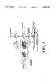
- FIG. 1is a schematic depiction of a vapor immersion three-dimensional micromachining system constructed in accordance with the present invention
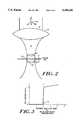
- FIG. 2is a schematic depiction of a microscope objective and beam focussing pattern in accordance with the invention
- FIG. 3shows the theoretical characteristic of a substantially binary reaction induced in accordance with the present invention
- FIG. 4shows an example of behavior of a substantially binary silicon etching reaction in accordance with the present invention
- FIGS. 5A-5Care schematic depictions of an illustrative etching of a three-dimensional object in accordance with the invention.
- FIG. 6is a schematic representation of an illustrative microchemical reaction induced in accordance with the invention.
- FIG. 7is a schematic representation of a field-imaging system suitable for use with the invention.
- FIG. 8is a schematic depiction of a microfluidic circuit constructed in accordance with the invention.
- FIG. 9Ais a schematic plan view of a microfluidic circuit constructed in accordance with the invention.
- FIG. 9Bis a perspective schematic view of a fiber-optic cable coupling device constructed in accordance with the invention.
- one aspect of the inventionfeatures a micromachining method for making three-dimensional objects in a size regime one to two orders of magnitude smaller than that of conventional machine tools. That is, objects made according to this invention may range in size from ten cubic micrometers to ten cubic centimeters.
- the methodutilizes fast, laser activated microchemical reactions to provide levels of resolution and versatility in the formation of the object profile in the third dimension which have been heretofore unachievable.
- the inventive conceptinvolves the architecture of layers. By successively forming two-dimensional patterns of finite thickness, through either etching in a substrate or deposition, a three-dimensional structure is formed.
- the inventionutilizes non-linear microchemical reactions initiated by a beam of radiant energy which varies in beam density level to confine the reaction zone thereby providing exceptionally high resolution in three dimensions.
- FIG. 1An illustrative system for carrying out the process of the invention is schematically shown in FIG. 1.
- a laser source 10directs a beam of radiant energy 12 through an X-Y scanner 14. While a laser source 10 and laser beam 12 are shown and discussed below in detail, those skilled in the art will appreciate that the concepts of the invention are equally applicable to other types of energy beams such as, for example, electron and focused ion beams. Other beams will, of course, require other known scanning techniques.
- the X-Y scannerincludes a pair of TeO 2 driven acousto-optic deflectors 16 for addressing a field of 256 ⁇ 256 pixels. Other means for deflecting the beam 12 in the X-Y plane will be apparent to those skilled in the art.
- a two axis galvo systemcan be used to scan a continuous-wave or pulsed laser.
- a third acousto-optic deflector 17compensates in real time for the non-uniform transmission of the deflectors across the scan field.
- the 256 ⁇ 256 pixel fieldcan be addressed at speeds up to 50,000 pixels per second.
- the fieldIn raster mode the field can be addressed at up to 2.5 million pixels per second. This speed is limited, in the random access mode, by the acoustic wave stabilization time of approximately ten microseconds per address point.
- the beam 12travels to beam splitters 18 and 20.
- the beam splittersafford the ability to monitor the reaction zone and thereby provide feedback data.
- a CCD camera 22is utilized for monitoring the reaction zone and registering the scan to existing structure on the substrate.
- an illuminator 24, such as a helium neon laser beam, introduced through beam splitter 20 into the focussing optics of the camera 22,can be detected in retroreflection and used to automatically maintain focus over extended X-Y travel by means of a spot minimization algorithm.
- the beam 12travels to a microscope objective 26 which is fixed to a stage 28 ("Z-stage") for moving the microscope objective 26 in the Z direction.
- the microscope objective 26critically focuses the beam to an interface plane 30 in a chamber 32.
- the Z stageis driven by a stepping motor (not shown) for displacing the microscope objective 26 to refocus the beam to successive interface planes for the successive patterning of layers.
- a suitable numerical aperture of the microscope objectiveis in the range of 0.1 to 0.9 and preferably is 0.25. This yields a nearly diffraction limited one micrometer focal spot.
- a reactive vapor ambientis maintained in chamber 32 via gas inlet 34 and gas outlet 36.
- the microchemical reaction conditionscan be maintained to produce nominal one micrometer by one micrometer by one micrometer pixel address points. In some etching applications, however, a vacuum is maintained in the chamber 32.
- an important feature of the inventionis that a critically focussed beam of radiant energy induces a non-linear microchemical reaction.
- the microchemical reactions of the inventionare non-linear, or binary, in that they essentially self-extinguish absent exposure to radiant energy above a prescribed intensity.
- the beam 12varies in beam density level so that it is only above the prescribed intensity at a certain points along the beam.
- FIG. 2shows that after the beam 12 passes through the microscope objective 26 it is focussed down to a focal point 42 at the interface plane 30. Confining the radiant energy of the prescribed intensity to the focal point 42 restricts any microchemical reactions induced by that radiant energy to this zone. Accordingly, the focal point 42 can be referred to as a reaction zone.
- the microchemical reactionself-extinguishes since the focal point 42 is no longer focussed at what has become the new interface plane 31.
- the reactionwill self-extinguish when material has been removed to the extent of line 29 due to the position of what has become the new interface plane 29 in respect to the focal point 42.
- the focal pointmust be scanned in the X-Y plane and stepped in the Z direction to continue to form the object. This is described below in greater detail.
- the reactionis confined along the substrate since it self-extinguishes abruptly at a distance where the beam-induced temperature of the substrate falls below the critical value.
- the substratemay be tilted relative to the Z-axis, but regions where the beam-induced temperature falls below the critical value will not be modified.
- the height of each pixelis accurately controlled by this effect and by accurately timing the beam dwell.
- the binary characteristic of the reactionis useful for this means of controlling height since the saturation means that an accurate height is achieved across the pixel and also that focal point dwell time is directly proportional to pixel height.
- FIG. 3shows the theoretical characteristic of a substantially binary reaction where the rate of deposition or etching substantially self extinguishes below a prescribed beam power, for a continuous wave beam, or beam fluence, for a pulsed beam.
- a prescribed levelis indicated as Pt.
- the reactionsaturates to a nearly constant rate at higher powers.
- the range of nearly-constant rateshould be over a parameter window which is easily controlled by the laser apparatus so that even when fluctuations in the source or optical apparatus are present, the nominal laser intensity can be set so that the reaction can be considered either substantially fully “on” or substantially fully “off.”
- FIG. 4shows typical behavior of a well-constructed substantially binary chemical reaction for the specific case of silicon etching with 488-nm light in a 250 Torr chlorine atmosphere.
- the vertical axisshows the measured etch rate plotted for various dwell times ranging from 32 to 1028 microseconds.
- the horizontal axisis laser power. Note that the reaction rate rises rapidly from an immeasurable value (less than 2 ⁇ 10 2 micrometers per second) to greater than 3 ⁇ 10 3 micrometers per second with an increase in laser power from approximately 600 milliwatts to 700 milliwatts. The reaction rate then varies only slightly at laser powers greater than 800 milliwatts.
- a useful etchant gas for silicon patterningis undiluted chlorine at a pressure of 1 to 2000 Torr.
- Other halogen-containing vaporsincluding SF 6 , CF 4 , CCl 4 , and various freons are also useful.
- Preferred pressure conditionstypically range between 10 and 2000 Torr.
- these gasesare effective etchants for germanium, molybdenum, tungsten and other metals.
- a diluentcan be added to the etchant gas to moderate etching in the halogen component.
- a 0.01 Torr to 100 Torr oxygen gas diluentstabilizes the laser etching, although it also slows the etch rate.
- a wavelength shorter than approximately 500 nanometerswill often be more effective since these metals become more strongly absorbent at these shorter wavelengths.
- Depositioncan be achieved using the nearly binary pyrolysis reaction for silane.
- Typical parameters for good deposition of polysilicon structuresare approximately 200 Torr of undiluted silane, using a power per unit beam diameter of one to five kilowatts per centimeter at 488-nanometer wavelength on a silicon substrate.
- Chromium oxide structurescan be deposited at 0.1 to two kilowatts per centimeter power on the same silicon substrate material using between one and ten Torr of chromium oxychloride as a vapor precursor.
- the substrateis placed in the chamber 32 while a slowly flowing (one standard cubic centimeter per minute) ambient of chlorine gas is passed through the chamber which is maintained at approximately 100 Torr.
- the laser source 10for example, a CW argon-ion laser, operates at 488 nanometers to deliver 900 milliwatts of power.
- a focal point of approximately one micrometer in depth and diameteris scanned across the surface of the substrate at approximately 7500 micrometers per second. This results in a dwell time of approximately 133 microseconds per pixel.
- the radiant energyraises the temperature of each one micrometer cubic pixel of silicon to just above its melting point. Under the above-stated conditions, this occurs at an instant power per unit beam radius slightly exceeding 5 ⁇ 10 3 watts per centimeter.
- a quasi-equilibrium thermal profileaccrues in the solid exposed to the focal point 42 in a time scale less than a microsecond.
- the locally effected regionis well confined to the area of the silicon near the one micrometer diameter radiated zone by the rapidly diverging steady state heat flow into the semi-infinite solid. Scanning speed is maintained fast enough to modify the layer in accordance with the non-linear localized reaction.
- the surface of the molten zonereacts with the chlorine ambient at a rate within an order of magnitude of the chlorine surface collision frequency. This is believed to be among the fastest known sustained gas/surface interfacial chemical reactions because of the extreme efficiency of the chemical path, the small zone size, and the reduction of transport limitations from boundary layer accumulation.
- the initial vapor phase productis believed to predominantly comprise SiCl 2 . This product is eventually converted to SiCl 4 in the cooling vapor stream flowing out of gas outlet 36.
- a first layer ⁇ Z 1can be created by etching, for example, by way of the above-described microchemical reaction. This is achieved by positioning microscope objective 26 to focus focal point 42 of beam 12 at the interface plane 30, which in this case is defined by the upper surface of silicon body 40. The beam 12 is scanned to the right in the Figure to etch a pattern in the X-Y plane of the body having a a depth corresponding to the thickness of layer ⁇ Z 1 . Typically, that thickness is approximately one micrometer.
- a new interface plane 30'is exposed.
- the microscope objective 26is then stepped down by way of Z stage 28 to focus focal point 42 on the new interface plane 30'. This results in a second layer ⁇ Z 2 being etched.
- a new interface plane 30"is exposed.
- the microscope objectiveis again stepped via Z stage 28 for etching a layer ⁇ Z 3 in silicon body 40.
- material removal volumescan be so small at each address point that stepping increments can create essentially curved surfaces. This is an advantage over, for example, mask-based lithographic processes in which only flat surfaces can be formed.
- Material removal rates of approximately 2 ⁇ 10 4 cubic micrometers per secondhave been achieved with the above described silicon chlorine system utilizing a 900 milliwatt laser power in conjunction with one micrometer focal point size, while maintaining a vapor atmosphere of approximately 400 Torr.
- This removal rateis nearly time independent and only weakly dependent upon scanning speed and laser power.
- Changing the laser dwell time at each pixelalters the etched depth in a nearly linear fashion and can thereby be exploited to accurately control depth.
- a larger dynamic range in etch ratecan be obtained by altering the pressure in the chamber.
- a laser dwell time of as small as one microsecondcan be utilized to provide a material removal rate as small as 2 ⁇ 10 -2 micrometer depth per dwell.
- a high chamber pressurecan be coupled with the largest focal point diameter which is consistent with the required degree of resolution and available beam power.
- volumetric etching rates of greater than 2 ⁇ 10 5 cubic micrometers per secondcan be achieved using a ten micrometer focal point size and a 300 Torr chamber pressure.
- the inventionprovides at least two distinct advantages over known methods for micromachining. These advantages include significantly greater resolution than has been heretofore achievable, and the ability to vary the profile of an object in the third dimension.
- the X-Y resolution of the processdepends on the confinement of the molten silicon zone. Because of the non-linearity of the phase transition and the efficient heat spreading into the solid, this zone can be significantly smaller than the diffraction-limited beam diameter. For example, using a visible light beam with 0.5 numerical aperture focussing optics in cooperation with thermal chlorine reactions, 0.2 micrometer line widths in silicon have been achieved. Vertical resolution (in the Z direction) is controlled by timing the duration of the melt and, if necessary, by slowing the reaction through reduced chamber pressure.
- the etch depthbecomes 1 nanometer per 10 microsecond temporal resolution element.
- Modifying the laser beam intensity distribution using beam-shaping opticscan be used to create "laser tool-bits" which can be used to control the reaction profile by changing the thermal patterns in the work-piece.
- the thin layer of regrown siliconis comparable in quality to that resulting from laser annealing. In most cases, this is quite sufficient for the formation of high performance electronic devices.
- Polishing of structurescan be accomplished by reducing the laser power below the melt threshold and making use of the photochemical reaction driven by vapor phase laser photolysis of the atmosphere in the chamber.
- the photolysis reactionproduces a plume of chlorine atoms which is reactive well below the silicon melting point.
- nearly one percent of the chlorine gascan be photochemically activated at approximately 50 Torr Cl 2 pressure. While this photochemical mechanism is typically three to four orders of magnitude slower than the thermal process, its low temperature and slow rate make it attractive as a method for polishing structures which have been thermally laser-etched.
- Another patterning strategyis to use a pulsed laser in either a scanned focused or field-imaged mode.
- Pixel heightcan then be controlled by the non-linear, binary, reaction as discussed above and the timed exposure supplied by the duration of the laser pulse.
- a 308 nm wavelength laser using a 20-nanosecond pulse durationcan be used to induce a solid-to-vapor phase transition of polyimide in an air or vacuum ambient and thereby etch 0.1 to 1 micrometer deep pixels with each pulse.
- the reactionis of the phase transition solid-to-vapor type with a concomittant chemical degradation of the polyimide.
- the pulse repetition ratecan be varied from 1 to 400 pulses per second to control material removal rate.
- the required fluence for this reactionis typically 50 to 400 millijoules per square centimeters.
- Preferred conditions for patterning polyimideare 150 millijoules per square centimeter at 308 nm wavelength. Under these conditions, approximately 0.2 micrometer depth of material is removed with each laser pulse in either ambient case. Vacuum irradiation, however, results in cleaner etching.
- a field-imaged mode systemis schematically shown in FIG. 7 wherein a light-valve array device 70 is illuminated with a pulsed laser beam 72 and images the beam 72 to a lens 74 for focussing onto an interface plane 76 on a workpiece 78.
- a reflection or transmission light valve arraycan be used, provided a fluence above the critical value for the non-linear reaction is achieved.
- the light-valve device 70is reconfigured in time without scanning the work piece. Those skilled in the art will be familiar with reflective and transmissive light valve devices.
- the light-valve array 70is electronically reconfigured in a known manner and the work piece 78 is stepped in the Z direction either toward or away from the lens 74. Irradiation of the next plane of pixels is then begun. After the full three-dimensional structure is achieved, the workpiece is stepped to the next field site and the process is repeated.
- Etching of polyimideprovides an excellent example for patterning with a UV laser in the field-imaged mode.
- numerous organic and inorganic materialsmay also be etched including metal-oxide ceramics and metals. Short pulses, 30 nanoseconds or less, are preferred for most materials since non-linear reaction conditions are achieved more easily.
- the field-imaged modecan also be adapted for deposition. In this case the nonlinear reaction is used to deposit a pattern of material from a gas phase precursor. For example, silicon can be deposited from disilane using a 193 nm laser.
- the disilane pressurewill preferably range from approximately 10 Torr to approximately 100 Torr and the incident laser fluence will range from 50 to 500 millijoules per square centimeter.
- an effective mode of operationis to use a 128 pixel by 128 pixel light valve array with reflective sixty micrometer by sixty micrometer pixels. The array is imaged onto the work piece at a five times reduction factor so that a field of 16,384 squares, each twelve micrometers across, can be etched or deposited.
- the imaging lensmay be an all-reflective optic if necessary for UV wavelengths less than approximately 250 nanometers.
- Fluence at the light valve arrayis preferably adjusted to be approximately equal to 4RE millijoules per square centimeter where R is the light valve reflectively and E is the imaging-system efficiency.
- the laseris fired at a repetition frequency of 200 hertz for approximately 0.25 second.
- the light valve arrayis then electronically reconfigured in a switching time less than 0.1 second and the laser is again fired to etch the next layer pattern.
- Numerous laser deposition and etching processescan be implemented, many of which are described in the book "Laser Microfabrication: Thin Film Processes and Lithography, Edition by D. J. Ehrlich and J. Y. Tsao (Academic Press, Boston, 1989).
- the processes and system of the inventionare suitable for the formation of a wide array of microelectromechanical devices.
- this class of deviceshas been impractical because of the difficulty of making microscopic three-dimensional surfaces.
- ithas been impractical to make three-dimensional smooth curves of prescribed shape which are essential for well-designed flow devices.
- Ithas furthermore been impossible to design and implement microchannel structures at fine dimension directly from a computer-aided-design file without the significant time delays characteristic of microfabrication using conventional photomasks.
- the design and fabrication of complicated devicescan be carried out in minutes or hours. This is critical in commercial applications in which great value is placed on the speed with which a custom device can be delivered to the marketplace.
- a microfluidic "standard cell” class of devices analogous to semiconductor electronic circuitscan be developed and stored in a computer file.
- the "standard cells”can be three-dimensional microstructures such as flow channels, branches, valve seats, pump seats, and detector elements. A designer can then recall these "standard cells” and assemble them at a computer-aided-design terminal into a custom fluidic system. Data from the terminal can then be sent directly to a laser scanner or light valve array thereby allowing a prototype device to be etched or deposited in minutes. Multiple copies of the device can be manufactured by making molds in this fashion and by then stamping out multiple copies using known replication techniques.
- a broad class of integrated microfluidic circuitscan be developed around the construct of functional layers in this manner. These circuits include devices such as valves, pumps, plumbing manifolds, chemical sensors, physical sensors (such as pressure and temperature) and heat exchangers.
- thermal isolation structures integrated into the native silicon water with electronicsmay allow more flexibility in dissipating heat.
- the devicesare miniaturized and interconnected at high density in order to gain the advantages of high complexity, small fluid volume, high sampling speed, reliability, and low fabrication costs. They are extremely well suited for the processing of precious fluids. Moreover, their small size lends itself to low material costs, ease of implantability and portability.
- microfluidic systemscan be utilized for high speed chemical analysis using expensive reagents or pharmaceuticals, the synthesis of macromolecules by high speed switching of flows, the detection of nerve or chemical warfare agents, the detection of drugs, and as physiological monitors. Additionally, the systems can be utilized in forensic, chemical and genetic engineering applications for the sequencing of genetic material. Macroscopic dimensioned fluid systems are impractical for applications such as these for various reasons including the cost of reagent fluids and the cost of constructing highly branched macrofluidic system.
- FIG. 8schematically shows a cleaved silicon wafer 50 with a layer of thermal oxide 52.
- the above discussed microchemical reactionsare induced by scanning the laser focal point under the transparent oxide film 52 to create a flow channel 54 beneath the oxide layer 52.
- the developing channel 54allows flow of vapor phase reactants and products in and out of the reaction zone to sustain the reaction.
- An electronic device layersuch as a thin film piezoelectric layer 55 and metallization film 56, may be added to provide, for example, an actuator layer for the valve and pumps formed in the substrate by the above described laser techniques.
- Other activator layerscould use lead-lanthanum-zirconium-titanium (PLZT), zinc oxide or other electro-mechanical thin films.
- PZTlead-lanthanum-zirconium-titanium
- electronicscan be formed on a separate chip and connected to the microchip by hybrid or multi-chip module technology. They can be either fabricated on a separate substrate and bonded or laminated to a first substrate containing the passive structures.
- a good choice of the actuator filmis sol-gel deposited lead zirconium titanate.
- the electrode layer 56can be platinum.
- FIG. 9Ashows a plan view of a typical microfluidic standard cell 100 that can be fabricated by the above-described techniques.
- the cell 100includes a flow path 102 have inlet port 104 and outlet port 106. Additionally, a pump 108 and a valve 110 control flow through the flow path 102.
- the coupling 200is a precision mechanical structure for aligning a fiber optic cable 202 with a laser 204.
- Other micro-optic applicationsinclude the precision machining of various types of refractive and diffractive optics.
- laser deposition using the processes citedcan be used to attach devices, to optimize optoelectronic components, and to customize performance.
- Laser three-dimensional etchingcan be used for the fabrication of wells, mirrors, and other optoelectronic structures, and to adjust the dimensions of partially fabricated systems.
- a further class of applications for the inventionis the assembly and packaging of microdevices.
- Previouslythere have been limited techniques for microscopic operations akin to, for example, welding at macroscopic dimension.
- the inventionit is possible to assemble and repair three-dimensional parts at microscopic scales.
- a microscopic cotter pincan be created by depositing from silane gas a twenty micrometer silicon ball on the end of a ten micrometer bearing post to fix a one-hundred micrometer, or smaller, gear on an end of the post.
- a three-dimensional silicon nitride wear padcould be created on this structure as well.
- the systemcan be utilized for in etching vias through a silicon wafer to allow subsequent passivation and metallization for through wafer contacts. This is because these scanning mechanisms retain the high beam energy required for this type of operation.
- Potential applications for this processinclude isolation of one side of a circuit from a harmful environment such as the type to which various micro-chemical sensors might be exposed.
- the sensing agentmay be on one side of a wafer while the electronics is on the other side.
Landscapes
- Engineering & Computer Science (AREA)
- Physics & Mathematics (AREA)
- Optics & Photonics (AREA)
- Toxicology (AREA)
- Mechanical Engineering (AREA)
- Health & Medical Sciences (AREA)
- General Physics & Mathematics (AREA)
- Environmental & Geological Engineering (AREA)
- Chemical & Material Sciences (AREA)
- Manufacturing & Machinery (AREA)
- Materials Engineering (AREA)
- Microelectronics & Electronic Packaging (AREA)
- Plasma & Fusion (AREA)
- Drying Of Semiconductors (AREA)
Abstract
Description
Claims (33)
Priority Applications (1)
| Application Number | Priority Date | Filing Date | Title |
|---|---|---|---|
| US07/828,247US5389196A (en) | 1992-01-30 | 1992-01-30 | Methods for fabricating three-dimensional micro structures |
Applications Claiming Priority (1)
| Application Number | Priority Date | Filing Date | Title |
|---|---|---|---|
| US07/828,247US5389196A (en) | 1992-01-30 | 1992-01-30 | Methods for fabricating three-dimensional micro structures |
Publications (1)
| Publication Number | Publication Date |
|---|---|
| US5389196Atrue US5389196A (en) | 1995-02-14 |
Family
ID=25251261
Family Applications (1)
| Application Number | Title | Priority Date | Filing Date |
|---|---|---|---|
| US07/828,247Expired - LifetimeUS5389196A (en) | 1992-01-30 | 1992-01-30 | Methods for fabricating three-dimensional micro structures |
Country Status (1)
| Country | Link |
|---|---|
| US (1) | US5389196A (en) |
Cited By (45)
| Publication number | Priority date | Publication date | Assignee | Title |
|---|---|---|---|---|
| US5631463A (en)* | 1992-09-01 | 1997-05-20 | Canon Kabushiki Kaisha | Displacement element, probe employing the element, and apparatus employing the probe |
| US5641391A (en)* | 1995-05-15 | 1997-06-24 | Hunter; Ian W. | Three dimensional microfabrication by localized electrodeposition and etching |
| US5786023A (en)* | 1996-02-13 | 1998-07-28 | Maxwell; James L. | Method and apparatus for the freeform growth of three-dimensional structures using pressurized precursor flows and growth rate control |
| EP0863543A3 (en)* | 1997-03-03 | 1999-01-27 | Schlumberger Technologies, Inc. | Through-the-substrate investigation of flip-chip IC's |
| US5874011A (en)* | 1996-08-01 | 1999-02-23 | Revise, Inc. | Laser-induced etching of multilayer materials |
| US6033721A (en)* | 1994-10-26 | 2000-03-07 | Revise, Inc. | Image-based three-axis positioner for laser direct write microchemical reaction |
| WO2000072221A1 (en)* | 1999-05-24 | 2000-11-30 | Potomac Photonics, Inc. | Patterned surface cleaning system of miniature structures |
| WO2000072224A1 (en)* | 1999-05-24 | 2000-11-30 | Potomac Photonics, Inc. | Material delivery system for miniature structure fabrication |
| WO2000072222A1 (en)* | 1999-05-24 | 2000-11-30 | Potomac Photonics, Inc. | Apparatus for fabrication of miniature structures |
| WO2000072223A1 (en)* | 1999-05-24 | 2000-11-30 | Potomac Photonics, Inc. | A pulse-position system for miniature structures |
| US6253116B1 (en) | 1998-08-04 | 2001-06-26 | New Jersey Institute Of Technology | Method and apparatus for rapid freezing prototyping |
| US20010045525A1 (en)* | 2000-01-21 | 2001-11-29 | Gerlach Robert L. | Shaped and low density focused ion beams |
| US20020182877A1 (en)* | 2001-04-09 | 2002-12-05 | Marc Nantel | Photo-processing of materials in the presence of reactive fluid |
| US20030011789A1 (en)* | 2001-06-29 | 2003-01-16 | Lyle Shirley | Apparatus and methods for optically monitoring thickness |
| US6623860B2 (en) | 2000-10-10 | 2003-09-23 | Aclara Biosciences, Inc. | Multilevel flow structures |
| US6649861B2 (en) | 2000-05-24 | 2003-11-18 | Potomac Photonics, Inc. | Method and apparatus for fabrication of miniature structures |
| US6674058B1 (en) | 2000-09-20 | 2004-01-06 | Compucyte Corporation | Apparatus and method for focusing a laser scanning cytometer |
| WO2003055660A3 (en)* | 2001-10-26 | 2004-01-22 | Aclara Biosciences Inc | System and method for injection molded micro-replication of micro-fluidic substrates |
| US20040099636A1 (en)* | 2002-11-21 | 2004-05-27 | Lawrence Scipioni | Fabrication of three dimensional structures |
| US20040140438A1 (en)* | 2001-01-19 | 2004-07-22 | Gerlach Robert L. | Angular aperture shaped beam system and method |
| US6792326B1 (en)* | 1999-05-24 | 2004-09-14 | Potomac Photonics, Inc. | Material delivery system for miniature structure fabrication |
| US20040190573A1 (en)* | 2003-03-24 | 2004-09-30 | Eastman Kodak Company | Electronic imaging system using organic laser array illuminating an area light valve |
| US6835426B2 (en)* | 2001-01-19 | 2004-12-28 | Potomac Photonics, Inc. | Method and apparatus for pulse-position synchronization in miniature structures manufacturing processes |
| US20050006136A1 (en)* | 2003-06-11 | 2005-01-13 | Arnold Craig B. | Laser-based technique for producing and embedding electrochemical cells and electronic components directly into circuit board materials |
| US6862490B1 (en)* | 1999-05-24 | 2005-03-01 | Potomac Photonics, Inc. | DLL circuit taking acount of external load |
| US6878567B2 (en)* | 2001-06-29 | 2005-04-12 | Intel Corporation | Method and apparatus for fabrication of passivated microfluidic structures in semiconductor substrates |
| US20070086822A1 (en)* | 2003-11-10 | 2007-04-19 | Technology Transfer Service Corp. | Laser marking device, laser marking method, and object to be marked |
| US7261542B2 (en) | 2004-03-18 | 2007-08-28 | Desktop Factory, Inc. | Apparatus for three dimensional printing using image layers |
| US20080067160A1 (en)* | 2006-09-14 | 2008-03-20 | Jouni Suutarinen | Systems and methods for laser cutting of materials |
| US20090255110A1 (en)* | 2006-02-03 | 2009-10-15 | United Technologies Corporation | Photo-etched edm electrode |
| US20090266804A1 (en)* | 2008-04-24 | 2009-10-29 | Costin Darryl J | Combination extrusion and laser-marking system, and related method |
| US20110134420A1 (en)* | 2008-07-22 | 2011-06-09 | Daisuke Matsumoto | Microchip and Analyzing Apparatus |
| US8224189B1 (en) | 2007-02-02 | 2012-07-17 | Sunlight Photonics Inc. | Retro-directive target for free-space optical communication and method of producing the same |
| WO2015128783A1 (en)* | 2014-02-28 | 2015-09-03 | Ettore Maurizio Costabeber | Improved stereolithography machine |
| US9141786B2 (en) | 1996-11-08 | 2015-09-22 | Finjan, Inc. | Malicious mobile code runtime monitoring system and methods |
| US9219755B2 (en) | 1996-11-08 | 2015-12-22 | Finjan, Inc. | Malicious mobile code runtime monitoring system and methods |
| WO2016100873A1 (en)* | 2014-12-18 | 2016-06-23 | The Regents Of The University Of Colorado, A Body Corporate | Novel methods of atomic layer etching (ale) using sequential, self-limiting thermal reactions |
| US20160207141A1 (en)* | 2015-01-21 | 2016-07-21 | Agie Charmilles New Technologies Sa | Laser Ablation Method with Patch Optimization |
| US20180043618A1 (en)* | 2015-03-02 | 2018-02-15 | The Board Of Regents, The University Of Texas System | Embedding apparatus and method utilizing additive manufacturing |
| US10208383B2 (en) | 2017-02-09 | 2019-02-19 | The Regents Of The University Of Colorado, A Body Corporate | Atomic layer etching processes using sequential, self-limiting thermal reactions comprising oxidation and fluorination |
| US10256108B2 (en) | 2016-03-01 | 2019-04-09 | Lam Research Corporation | Atomic layer etching of AL2O3 using a combination of plasma and vapor treatments |
| US10552603B2 (en) | 2000-05-17 | 2020-02-04 | Finjan, Inc. | Malicious mobile code runtime monitoring system and methods |
| US10787744B2 (en) | 2016-05-23 | 2020-09-29 | The Regents Of The University Of Colorado, A Body Corporate | Enhancement of thermal atomic layer etching |
| US11165408B2 (en)* | 2017-08-02 | 2021-11-02 | Disco Corporation | Method of manufacturing substrate for acoustic wave device |
| US11179697B2 (en) | 2014-02-03 | 2021-11-23 | International Business Machines Corporation | Flow cell array and uses thereof |
Citations (9)
| Publication number | Priority date | Publication date | Assignee | Title |
|---|---|---|---|---|
| US4331504A (en)* | 1981-06-25 | 1982-05-25 | International Business Machines Corporation | Etching process with vibrationally excited SF6 |
| US4615756A (en)* | 1984-07-11 | 1986-10-07 | Hitachi, Ltd. | Dry etching apparatus |
| US4615904A (en)* | 1982-06-01 | 1986-10-07 | Massachusetts Institute Of Technology | Maskless growth of patterned films |
| US4622095A (en)* | 1985-10-18 | 1986-11-11 | Ibm Corporation | Laser stimulated halogen gas etching of metal substrates |
| US4834834A (en)* | 1987-11-20 | 1989-05-30 | Massachusetts Institute Of Technology | Laser photochemical etching using surface halogenation |
| US4929402A (en)* | 1984-08-08 | 1990-05-29 | 3D Systems, Inc. | Method for production of three-dimensional objects by stereolithography |
| US5081002A (en)* | 1989-04-24 | 1992-01-14 | The Trustees Of Columbia University In The City Of New York | Method of localized photohemical etching of multilayered semiconductor body |
| US5129991A (en)* | 1991-04-30 | 1992-07-14 | Micron Technology, Inc. | Photoelectron-induced selective etch process |
| US5232749A (en)* | 1991-04-30 | 1993-08-03 | Micron Technology, Inc. | Formation of self-limiting films by photoemission induced vapor deposition |
- 1992
- 1992-01-30USUS07/828,247patent/US5389196A/ennot_activeExpired - Lifetime
Patent Citations (9)
| Publication number | Priority date | Publication date | Assignee | Title |
|---|---|---|---|---|
| US4331504A (en)* | 1981-06-25 | 1982-05-25 | International Business Machines Corporation | Etching process with vibrationally excited SF6 |
| US4615904A (en)* | 1982-06-01 | 1986-10-07 | Massachusetts Institute Of Technology | Maskless growth of patterned films |
| US4615756A (en)* | 1984-07-11 | 1986-10-07 | Hitachi, Ltd. | Dry etching apparatus |
| US4929402A (en)* | 1984-08-08 | 1990-05-29 | 3D Systems, Inc. | Method for production of three-dimensional objects by stereolithography |
| US4622095A (en)* | 1985-10-18 | 1986-11-11 | Ibm Corporation | Laser stimulated halogen gas etching of metal substrates |
| US4834834A (en)* | 1987-11-20 | 1989-05-30 | Massachusetts Institute Of Technology | Laser photochemical etching using surface halogenation |
| US5081002A (en)* | 1989-04-24 | 1992-01-14 | The Trustees Of Columbia University In The City Of New York | Method of localized photohemical etching of multilayered semiconductor body |
| US5129991A (en)* | 1991-04-30 | 1992-07-14 | Micron Technology, Inc. | Photoelectron-induced selective etch process |
| US5232749A (en)* | 1991-04-30 | 1993-08-03 | Micron Technology, Inc. | Formation of self-limiting films by photoemission induced vapor deposition |
Non-Patent Citations (10)
| Title |
|---|
| "Laser Deposition and Etching on Three-Dimensional Microstructures;" Bloomstein et al.; Published in 1991 International Conf. on Solid-State Sensors and Actuators Digest of Technical Ppapers-pp. 508-511. |
| "Laser-Chemical Three-Dimensional Writing of Multimaterial Structures for Microelectromechanics:" Bloomstein et al.; Published in Proceedings for IEEE Micro Electro Mechanical Systems pp. 202-203; 1991. |
| "Making a Model and Doing It Fast;" The New York Times, Sunday, Sep. 23, 1990; p. F9. |
| "The Small Wonders of Microengineering;" Ivan Amato; Science, 26 Jul. 1991; pp. 387-388. |
| "Truly Three-Dimensional Structures Microfabricated by Laser Chemical Processing;" Westberg et al.; 91CH2817-May 1991 IEEE pp. 516-519. |
| Laser Chemical Three Dimensional Writing of Multimaterial Structures for Microelectromechanics: Bloomstein et al.; Published in Proceedings for IEEE Micro Electro Mechanical Systems pp. 202 203; 1991.* |
| Laser Deposition and Etching on Three Dimensional Microstructures; Bloomstein et al.; Published in 1991 International Conf. on Solid State Sensors and Actuators Digest of Technical Ppapers pp. 508 511.* |
| Making a Model and Doing It Fast; The New York Times, Sunday, Sep. 23, 1990; p. F9.* |
| The Small Wonders of Microengineering; Ivan Amato; Science, 26 Jul. 1991; pp. 387 388.* |
| Truly Three Dimensional Structures Microfabricated by Laser Chemical Processing; Westberg et al.; 91CH2817 May 1991 IEEE pp. 516 519.* |
Cited By (70)
| Publication number | Priority date | Publication date | Assignee | Title |
|---|---|---|---|---|
| US5631463A (en)* | 1992-09-01 | 1997-05-20 | Canon Kabushiki Kaisha | Displacement element, probe employing the element, and apparatus employing the probe |
| US6033721A (en)* | 1994-10-26 | 2000-03-07 | Revise, Inc. | Image-based three-axis positioner for laser direct write microchemical reaction |
| US5641391A (en)* | 1995-05-15 | 1997-06-24 | Hunter; Ian W. | Three dimensional microfabrication by localized electrodeposition and etching |
| US5786023A (en)* | 1996-02-13 | 1998-07-28 | Maxwell; James L. | Method and apparatus for the freeform growth of three-dimensional structures using pressurized precursor flows and growth rate control |
| US5874011A (en)* | 1996-08-01 | 1999-02-23 | Revise, Inc. | Laser-induced etching of multilayer materials |
| US9444844B2 (en) | 1996-11-08 | 2016-09-13 | Finjan, Inc. | Malicious mobile code runtime monitoring system and methods |
| US9189621B2 (en) | 1996-11-08 | 2015-11-17 | Finjan, Inc. | Malicious mobile code runtime monitoring system and methods |
| US9141786B2 (en) | 1996-11-08 | 2015-09-22 | Finjan, Inc. | Malicious mobile code runtime monitoring system and methods |
| US9219755B2 (en) | 1996-11-08 | 2015-12-22 | Finjan, Inc. | Malicious mobile code runtime monitoring system and methods |
| EP0863543A3 (en)* | 1997-03-03 | 1999-01-27 | Schlumberger Technologies, Inc. | Through-the-substrate investigation of flip-chip IC's |
| US6253116B1 (en) | 1998-08-04 | 2001-06-26 | New Jersey Institute Of Technology | Method and apparatus for rapid freezing prototyping |
| US6583381B1 (en)* | 1999-05-24 | 2003-06-24 | Potomac Photonics, Inc. | Apparatus for fabrication of miniature structures |
| WO2000072223A1 (en)* | 1999-05-24 | 2000-11-30 | Potomac Photonics, Inc. | A pulse-position system for miniature structures |
| WO2000072221A1 (en)* | 1999-05-24 | 2000-11-30 | Potomac Photonics, Inc. | Patterned surface cleaning system of miniature structures |
| US6862490B1 (en)* | 1999-05-24 | 2005-03-01 | Potomac Photonics, Inc. | DLL circuit taking acount of external load |
| WO2000072222A1 (en)* | 1999-05-24 | 2000-11-30 | Potomac Photonics, Inc. | Apparatus for fabrication of miniature structures |
| US6792326B1 (en)* | 1999-05-24 | 2004-09-14 | Potomac Photonics, Inc. | Material delivery system for miniature structure fabrication |
| WO2000072224A1 (en)* | 1999-05-24 | 2000-11-30 | Potomac Photonics, Inc. | Material delivery system for miniature structure fabrication |
| US20010045525A1 (en)* | 2000-01-21 | 2001-11-29 | Gerlach Robert L. | Shaped and low density focused ion beams |
| US6949756B2 (en)* | 2000-01-21 | 2005-09-27 | Fei Company | Shaped and low density focused ion beams |
| US10552603B2 (en) | 2000-05-17 | 2020-02-04 | Finjan, Inc. | Malicious mobile code runtime monitoring system and methods |
| US6649861B2 (en) | 2000-05-24 | 2003-11-18 | Potomac Photonics, Inc. | Method and apparatus for fabrication of miniature structures |
| US6674058B1 (en) | 2000-09-20 | 2004-01-06 | Compucyte Corporation | Apparatus and method for focusing a laser scanning cytometer |
| US6623860B2 (en) | 2000-10-10 | 2003-09-23 | Aclara Biosciences, Inc. | Multilevel flow structures |
| US20040140438A1 (en)* | 2001-01-19 | 2004-07-22 | Gerlach Robert L. | Angular aperture shaped beam system and method |
| US6835426B2 (en)* | 2001-01-19 | 2004-12-28 | Potomac Photonics, Inc. | Method and apparatus for pulse-position synchronization in miniature structures manufacturing processes |
| US20020182877A1 (en)* | 2001-04-09 | 2002-12-05 | Marc Nantel | Photo-processing of materials in the presence of reactive fluid |
| US7446382B2 (en)* | 2001-06-29 | 2008-11-04 | Intel Corporation | Method and apparatus for fabrication of passivated microfluidic structures in semiconductor substrates |
| US6878567B2 (en)* | 2001-06-29 | 2005-04-12 | Intel Corporation | Method and apparatus for fabrication of passivated microfluidic structures in semiconductor substrates |
| US20050090034A1 (en)* | 2001-06-29 | 2005-04-28 | Intel Corporation | Method and apparatus for fabrication of passivated microfluidic structures in semiconductor substrates |
| US6937350B2 (en) | 2001-06-29 | 2005-08-30 | Massachusetts Institute Of Technology | Apparatus and methods for optically monitoring thickness |
| US20030011789A1 (en)* | 2001-06-29 | 2003-01-16 | Lyle Shirley | Apparatus and methods for optically monitoring thickness |
| US20040195728A1 (en)* | 2001-10-26 | 2004-10-07 | Dennis Slomski | System and method for injection molded micro-replication of micro-fluidic substrates |
| WO2003055660A3 (en)* | 2001-10-26 | 2004-01-22 | Aclara Biosciences Inc | System and method for injection molded micro-replication of micro-fluidic substrates |
| US7160475B2 (en) | 2002-11-21 | 2007-01-09 | Fei Company | Fabrication of three dimensional structures |
| US20040099636A1 (en)* | 2002-11-21 | 2004-05-27 | Lawrence Scipioni | Fabrication of three dimensional structures |
| US20040190573A1 (en)* | 2003-03-24 | 2004-09-30 | Eastman Kodak Company | Electronic imaging system using organic laser array illuminating an area light valve |
| US6950454B2 (en)* | 2003-03-24 | 2005-09-27 | Eastman Kodak Company | Electronic imaging system using organic laser array illuminating an area light valve |
| US6986199B2 (en)* | 2003-06-11 | 2006-01-17 | The United States Of America As Represented By The Secretary Of The Navy | Laser-based technique for producing and embedding electrochemical cells and electronic components directly into circuit board materials |
| US20050006136A1 (en)* | 2003-06-11 | 2005-01-13 | Arnold Craig B. | Laser-based technique for producing and embedding electrochemical cells and electronic components directly into circuit board materials |
| US20070086822A1 (en)* | 2003-11-10 | 2007-04-19 | Technology Transfer Service Corp. | Laser marking device, laser marking method, and object to be marked |
| US7705870B2 (en)* | 2003-11-10 | 2010-04-27 | Arai Corporation | Laser marking device, laser marking method, and object to be marked |
| US7261542B2 (en) | 2004-03-18 | 2007-08-28 | Desktop Factory, Inc. | Apparatus for three dimensional printing using image layers |
| US20090255110A1 (en)* | 2006-02-03 | 2009-10-15 | United Technologies Corporation | Photo-etched edm electrode |
| US7618514B2 (en)* | 2006-02-03 | 2009-11-17 | United Technologies Corporation | Photo-etched EDM electrode |
| US20080067160A1 (en)* | 2006-09-14 | 2008-03-20 | Jouni Suutarinen | Systems and methods for laser cutting of materials |
| US8224189B1 (en) | 2007-02-02 | 2012-07-17 | Sunlight Photonics Inc. | Retro-directive target for free-space optical communication and method of producing the same |
| US20090266804A1 (en)* | 2008-04-24 | 2009-10-29 | Costin Darryl J | Combination extrusion and laser-marking system, and related method |
| US8436990B2 (en)* | 2008-07-22 | 2013-05-07 | Arkray, Inc. | Microchip and analyzing apparatus |
| US20110134420A1 (en)* | 2008-07-22 | 2011-06-09 | Daisuke Matsumoto | Microchip and Analyzing Apparatus |
| US11266970B2 (en)* | 2014-02-03 | 2022-03-08 | International Business Machines Corporation | Imaging multiple chemical reactions in a flow cell array |
| US11266971B2 (en) | 2014-02-03 | 2022-03-08 | International Business Machines Corporation | Imaging multiple chemical reactions in a flow cell array |
| US11179697B2 (en) | 2014-02-03 | 2021-11-23 | International Business Machines Corporation | Flow cell array and uses thereof |
| US11273426B2 (en) | 2014-02-03 | 2022-03-15 | International Business Machines Corporation | Imaging multiple chemical reactions in a flow cell array |
| US11266972B2 (en) | 2014-02-03 | 2022-03-08 | International Business Machines Corporation | Recording emission from multiple chemical reactions sites in a flow cell array |
| US11207654B2 (en) | 2014-02-03 | 2021-12-28 | International Business Machines Corporation | Flow cell array and uses thereof |
| CN106061715B (en)* | 2014-02-28 | 2018-06-19 | 埃托雷·毛里齐奥·科斯塔贝贝尔 | Improved stereo photoetching machine |
| WO2015128783A1 (en)* | 2014-02-28 | 2015-09-03 | Ettore Maurizio Costabeber | Improved stereolithography machine |
| CN106061715A (en)* | 2014-02-28 | 2016-10-26 | 埃托雷·毛里齐奥·科斯塔贝贝尔 | Improved stereolithography machine |
| US10381227B2 (en) | 2014-12-18 | 2019-08-13 | The Regents Of The University Of Colorado, A Body Corporate | Methods of atomic layer etching (ALE) using sequential, self-limiting thermal reactions |
| WO2016100873A1 (en)* | 2014-12-18 | 2016-06-23 | The Regents Of The University Of Colorado, A Body Corporate | Novel methods of atomic layer etching (ale) using sequential, self-limiting thermal reactions |
| US10486267B2 (en)* | 2015-01-21 | 2019-11-26 | Agie Charmilles New Technologies Sa | Laser ablation method with patch optimization |
| US20160207141A1 (en)* | 2015-01-21 | 2016-07-21 | Agie Charmilles New Technologies Sa | Laser Ablation Method with Patch Optimization |
| US20180043618A1 (en)* | 2015-03-02 | 2018-02-15 | The Board Of Regents, The University Of Texas System | Embedding apparatus and method utilizing additive manufacturing |
| US10256108B2 (en) | 2016-03-01 | 2019-04-09 | Lam Research Corporation | Atomic layer etching of AL2O3 using a combination of plasma and vapor treatments |
| US10784118B2 (en) | 2016-03-01 | 2020-09-22 | Lam Research Corporation | Atomic layer etching using a combination of plasma and vapor treatments |
| US10787744B2 (en) | 2016-05-23 | 2020-09-29 | The Regents Of The University Of Colorado, A Body Corporate | Enhancement of thermal atomic layer etching |
| US10208383B2 (en) | 2017-02-09 | 2019-02-19 | The Regents Of The University Of Colorado, A Body Corporate | Atomic layer etching processes using sequential, self-limiting thermal reactions comprising oxidation and fluorination |
| US11165408B2 (en)* | 2017-08-02 | 2021-11-02 | Disco Corporation | Method of manufacturing substrate for acoustic wave device |
| TWI761547B (en)* | 2017-08-02 | 2022-04-21 | 日商迪思科股份有限公司 | Manufacturing method of substrate for elastic wave device |
Similar Documents
| Publication | Publication Date | Title |
|---|---|---|
| US5389196A (en) | Methods for fabricating three-dimensional micro structures | |
| Bloomstein et al. | Laser‐chemical three‐dimensional writing for microelectromechanics and application to standard‐cell microfluidics | |
| Lim et al. | Fabrication of microfluidic mixers and artificial vasculatures using a high-brightness diode-pumped Nd: YAG laser direct write method | |
| US6649861B2 (en) | Method and apparatus for fabrication of miniature structures | |
| US6583381B1 (en) | Apparatus for fabrication of miniature structures | |
| US6783920B2 (en) | Photosensitive glass variable laser exposure patterning method | |
| US20040012124A1 (en) | Apparatus and method of fabricating small-scale devices | |
| US8393289B2 (en) | Laser assisted nano deposition | |
| EP0437043A2 (en) | Laser method and device for processing microcapsules or particles | |
| US7316748B2 (en) | Apparatus and method of dispensing small-scale powders | |
| Harvey et al. | Fabrication techniques and their application to produce novel micromachined structures and devices using excimer laser projection | |
| Holmes | Laser fabrication and assembly processes for MEMS | |
| US7053351B2 (en) | Near-field scanning optical microscope for laser machining of micro- and nano- structures | |
| Rizvi | Production of novel 3D microstructures using excimer laser mask projection techniques | |
| Livingston et al. | Variable UV laser exposure processing of photosensitive glass-ceramics: maskless micro-to meso-scale structure fabrication | |
| US6862490B1 (en) | DLL circuit taking acount of external load | |
| US20030071269A1 (en) | Apparatus and method for laser selective bonding technique for making sealed or enclosed microchannel structures | |
| Bertsch et al. | Microstereolithography: a review | |
| CN1313239C (en) | Laser Drilling System and Method Using Continuous Optimization of Depth of Focus | |
| Rizvi et al. | Laser micromachining: new developments and applications | |
| Mullenborn et al. | Fast 3D laser micromachining of silicon for micromechanical and microfluidic applications | |
| Christensen Jr | Waveguide excimer laser fabrication of 3D microstructures | |
| WO2003090937A1 (en) | Apparatus and method of fabricating small-scale devices | |
| JP2544520B2 (en) | Fine particle dynamics pattern | |
| TWI898259B (en) | Method for imaging a light beam onto an object, method for introducing an opening into a workpiece using the method, and device having an optical arrangement |
Legal Events
| Date | Code | Title | Description |
|---|---|---|---|
| AS | Assignment | Owner name:MASSACHUSETTS INSTITUTE OF TECHNOLOGY A CORPORATI Free format text:ASSIGNMENT OF ASSIGNORS INTEREST.;ASSIGNORS:BLOOMSTEIN, THEODORE M.;EHRLICH, DANIEL;FLYNN, ANITA M.;REEL/FRAME:006066/0399 Effective date:19920401 | |
| FEPP | Fee payment procedure | Free format text:PAYOR NUMBER ASSIGNED (ORIGINAL EVENT CODE: ASPN); ENTITY STATUS OF PATENT OWNER: LARGE ENTITY | |
| STCF | Information on status: patent grant | Free format text:PATENTED CASE | |
| FEPP | Fee payment procedure | Free format text:PAYER NUMBER DE-ASSIGNED (ORIGINAL EVENT CODE: RMPN); ENTITY STATUS OF PATENT OWNER: LARGE ENTITY | |
| FEPP | Fee payment procedure | Free format text:PAT HLDR NO LONGER CLAIMS SMALL ENT STAT AS NONPROFIT ORG (ORIGINAL EVENT CODE: LSM3); ENTITY STATUS OF PATENT OWNER: LARGE ENTITY Free format text:PAYOR NUMBER ASSIGNED (ORIGINAL EVENT CODE: ASPN); ENTITY STATUS OF PATENT OWNER: LARGE ENTITY Free format text:PAYER NUMBER DE-ASSIGNED (ORIGINAL EVENT CODE: RMPN); ENTITY STATUS OF PATENT OWNER: LARGE ENTITY | |
| FPAY | Fee payment | Year of fee payment:4 | |
| FPAY | Fee payment | Year of fee payment:8 | |
| FPAY | Fee payment | Year of fee payment:12 | |
| FEPP | Fee payment procedure | Free format text:PAYER NUMBER DE-ASSIGNED (ORIGINAL EVENT CODE: RMPN); ENTITY STATUS OF PATENT OWNER: LARGE ENTITY Free format text:PAYOR NUMBER ASSIGNED (ORIGINAL EVENT CODE: ASPN); ENTITY STATUS OF PATENT OWNER: LARGE ENTITY |