US5387445A - Liquid crystal display device - Google Patents
Liquid crystal display deviceDownload PDFInfo
- Publication number
- US5387445A US5387445AUS07/847,170US84717092AUS5387445AUS 5387445 AUS5387445 AUS 5387445AUS 84717092 AUS84717092 AUS 84717092AUS 5387445 AUS5387445 AUS 5387445A
- Authority
- US
- United States
- Prior art keywords
- liquid crystal
- resin
- compound
- light
- per molecule
- Prior art date
- Legal status (The legal status is an assumption and is not a legal conclusion. Google has not performed a legal analysis and makes no representation as to the accuracy of the status listed.)
- Expired - Lifetime
Links
Images

Classifications
- G—PHYSICS
- G02—OPTICS
- G02F—OPTICAL DEVICES OR ARRANGEMENTS FOR THE CONTROL OF LIGHT BY MODIFICATION OF THE OPTICAL PROPERTIES OF THE MEDIA OF THE ELEMENTS INVOLVED THEREIN; NON-LINEAR OPTICS; FREQUENCY-CHANGING OF LIGHT; OPTICAL LOGIC ELEMENTS; OPTICAL ANALOGUE/DIGITAL CONVERTERS
- G02F1/00—Devices or arrangements for the control of the intensity, colour, phase, polarisation or direction of light arriving from an independent light source, e.g. switching, gating or modulating; Non-linear optics
- G02F1/01—Devices or arrangements for the control of the intensity, colour, phase, polarisation or direction of light arriving from an independent light source, e.g. switching, gating or modulating; Non-linear optics for the control of the intensity, phase, polarisation or colour
- G02F1/13—Devices or arrangements for the control of the intensity, colour, phase, polarisation or direction of light arriving from an independent light source, e.g. switching, gating or modulating; Non-linear optics for the control of the intensity, phase, polarisation or colour based on liquid crystals, e.g. single liquid crystal display cells
- G02F1/133—Constructional arrangements; Operation of liquid crystal cells; Circuit arrangements
- G02F1/1333—Constructional arrangements; Manufacturing methods
- G02F1/1339—Gaskets; Spacers; Sealing of cells
- G—PHYSICS
- G03—PHOTOGRAPHY; CINEMATOGRAPHY; ANALOGOUS TECHNIQUES USING WAVES OTHER THAN OPTICAL WAVES; ELECTROGRAPHY; HOLOGRAPHY
- G03F—PHOTOMECHANICAL PRODUCTION OF TEXTURED OR PATTERNED SURFACES, e.g. FOR PRINTING, FOR PROCESSING OF SEMICONDUCTOR DEVICES; MATERIALS THEREFOR; ORIGINALS THEREFOR; APPARATUS SPECIALLY ADAPTED THEREFOR
- G03F7/00—Photomechanical, e.g. photolithographic, production of textured or patterned surfaces, e.g. printing surfaces; Materials therefor, e.g. comprising photoresists; Apparatus specially adapted therefor
- G03F7/004—Photosensitive materials
- G03F7/027—Non-macromolecular photopolymerisable compounds having carbon-to-carbon double bonds, e.g. ethylenic compounds
- G03F7/0275—Non-macromolecular photopolymerisable compounds having carbon-to-carbon double bonds, e.g. ethylenic compounds with dithiol or polysulfide compounds
- C—CHEMISTRY; METALLURGY
- C09—DYES; PAINTS; POLISHES; NATURAL RESINS; ADHESIVES; COMPOSITIONS NOT OTHERWISE PROVIDED FOR; APPLICATIONS OF MATERIALS NOT OTHERWISE PROVIDED FOR
- C09K—MATERIALS FOR MISCELLANEOUS APPLICATIONS, NOT PROVIDED FOR ELSEWHERE
- C09K2323/00—Functional layers of liquid crystal optical display excluding electroactive liquid crystal layer characterised by chemical composition
- C09K2323/05—Bonding or intermediate layer characterised by chemical composition, e.g. sealant or spacer
- C09K2323/057—Ester polymer, e.g. polycarbonate, polyacrylate or polyester
- G—PHYSICS
- G02—OPTICS
- G02F—OPTICAL DEVICES OR ARRANGEMENTS FOR THE CONTROL OF LIGHT BY MODIFICATION OF THE OPTICAL PROPERTIES OF THE MEDIA OF THE ELEMENTS INVOLVED THEREIN; NON-LINEAR OPTICS; FREQUENCY-CHANGING OF LIGHT; OPTICAL LOGIC ELEMENTS; OPTICAL ANALOGUE/DIGITAL CONVERTERS
- G02F2202/00—Materials and properties
- G02F2202/02—Materials and properties organic material
- G02F2202/022—Materials and properties organic material polymeric
- G02F2202/023—Materials and properties organic material polymeric curable
Definitions
- This inventionrelates to the use of a light curable resin composition for the sealing and/or encapsulation and/or inner construction of a liquid crystal cell and to the derived liquid crystal display device.
- a liquid crystal cell suitable for use as a display deviceis formed by bonding together at their peripheral parts two sheets or plates of an electrically insulating substrate, provided on their inner surfaces with transparent electrodes, using a sealant in the shape of a frame to maintain the substrates at a fixed and uniform distance apart and then feeding the liquid crystal material into the cell through a small inlet formed by leaving an aperture in the sealant and subsequently closing the inlet with an encapsulant.
- the sealant or encapsulantshould have excellent adhesion to the substrate, for example glass, and that it should not disturb the alignment of the liquid crystal and it is known to use a thermosetting epoxy resin for this purpose.
- a thermosetting epoxy resinfor this purpose.
- an epoxy resinneeds an extended high temperature cure, production line difficulties have been experienced.
- heating the resincan cause it to flow into the liquid crystal material so that the properties of the liquid crystal are adversely affected.
- cure at room temperaturenot only extends the cure time but also prolongs the contact time between the liquid crystal and the uncured epoxy resin so that low molecular weight ingredients of the resin diffuse into the liquid crystal bringing about a deterioration in performance by, for example, disturbing the alignment of the liquid crystal or lowering its insulation property.
- UV-curable resinsinclude radical polymerisation type resins in which acrylic monomers and oligomers are cured by photoinitiated radical polymerisation and cationic type resins in which an epoxy resin is cured by photoinitiated cationic polymerisation under the action of UV radiation and the like using an aromatic onium salt and the like as photoinitiator.
- the use of these resins for the sealing and/or encapsulation of liquid crystal cellshas been described in Japanese Patent Disclosures 59-93715 and 61-233719.
- certain light curable resin compositionscan be used for sealing and/or encapsulating and/or the inner construction of a liquid crystal cell and are able to provide stable liquid crystal cells having excellent working properties, the alignment of the liquid crystal remaining unaffected for long periods.
- the resin compositionsare especially suitable for encapsulating the liquid crystal inlet of the cell.
- the inventionprovides a liquid crystal display device including two electrically insulating substrates, electrodes on the inner surfaces of the substrates, a film of liquid crystal material contained between the electrodes and a resinous material as sealant and/or encapsulant and/or inner structural component characterised in that the resinous material is the product of light-curing a light-curable resin composition comprising at least one compound having two or more non-aromatic carbon-carbon unsaturated bonds per molecule, at least one compound having two or more mercapto groups per molecule and a photoinitiator.
- Inhibition of polymerisation by oxygen found in conventional light curable resin compositionsdoes not occur in the photopolymerisation reaction between a compound having at least two non-aromatic carbon-carbon unsaturated bonds per molecule (hereinafter referred to as a polyene) and a compound having at least two mercapto groups per molecule (hereinafter referred to as a polythiol).
- a polyenea compound having at least two non-aromatic carbon-carbon unsaturated bonds per molecule
- a polythiola compound having at least two mercapto groups per molecule
- the second componenta compound having at least two mercapto groups per molecule, may be represented by the general formula
- Ais an organic residue and q is an integer of 2 or more.
- polythiolsan ester of a thiol compound having a carboxyl group and a polyalcohol, for example trimethylolethane tris (mercaptoacetate), trimethylolethane tris (mercaptopropionate), trimethylolpropane tris(mercaptoacetate), trimethylolpropane tris (mercaptopropionate), pentaerythritol tetrakis (mercaptoacetate), pentaerythritol tetrakis (mercaptopropionate), ethylene glycol bis (mercaptoacetate), ethylene glycol bis (mercaptopropionate), polyethylene glycol bis (mercaptoacetate), polyethylene glycol bis (mercaptopropionate), dipentaerythritol hexakis (mercaptoacetate) and dipentaerythritol hexakis (mercaptopropionate), aliphatic polythiols, for example, dim
- a reaction product obtained by a reaction between a polyepoxy compound and a polythiola reaction product obtained by a reaction between a polyepoxy compound and thioglycolic acid and the like which have an average molecular weight more than 300.
- the essential criteria for the sealant and/or the encapsulant of the liquid crystal cellare that there should be no leakage of liquid crystal and no disturbance and/or disorder in liquid crystal alignment for a long period of time.
- the properties of the cured substancemay be freely varied in the above mentioned reaction product between an epoxy resin and a polythiol by means of properly selecting the molecular structure of the epoxy resin to be used.
- a phenolnovolak type resin or bisphenol A type resinmay be selected as an epoxy resin.
- a polyglycol type resinmay be selected.
- photopolymerization initiatorthere is no restriction on the photopolymerization initiator to be used.
- benzophenone, p-methoxybenzophenone, xanthone, chloroxanthone, m-chloro-acetophenone, propiophenone, anthraquinone, camphorquinone, trimethylbenzoyl diphenylphosphine oxide and benzilmay be mentioned but without limitation to these particular examples.
- a preferred mixing ratio of the components in the resin compositionis within a range between 1:0.1 and 1:3, and preferably in a range between 1:0.5 and 1:2 as a stoichiometric ratio of the non-aromatic carbon-carbon unsaturated bond in the polyene compound to SH group in the polythiol, but other ratios are not excluded.
- Suitable quantities of photopolymerization initiatorare within a range from 0.1 wt % to 5 wt % of the total quantity of the resin, but other amounts are not excluded.
- the viscosity of a resin compositionWhen encapsulating the inlet of the liquid crystal cell, if the viscosity of a resin composition is too low, the resin infuses deeply into the liquid crystal to adversely affect the performance of the liquid crystal cell and if the viscosity is too high, a suitable infusion of the resin into the liquid crystal inlet becomes difficult so that production problems occur.
- the preferred viscosity of the resin compositionis therefore within a range between 10 and 1000 poises and especially between 20 and 500 poises at 25° C.
- a polyene and/or a polythiol having a low viscositymay be used as a reaction diluent, or aerosil (fine particles of highly pure anhydrous silica; "Aerosil” is a registered trade mark of Nippon Aerosil) and the like maybe used as a viscosity improver or a thickener, but the usage of a polythiol of low viscosity can be troublesome in operation because of a strong offensive odour. It has been found that triallyl isocyanurate and triallyl cyanurate show an excellent dilution effect and also have high reactivity.
- the resin compositioncontains the aforementioned polythiol, polyene and photoinitiator as the essential components, but according to necessity or desire, may also contain such additives as an oxidation inhibitor, a polymerization inhibitor, a thixotropy improver, a silane coupling agent, a curing promoter and a filler.
- the light to be used for the curing of the light curable resin compositionmay be visible light or ultraviolet rays, or radiation containing both visible wave lengths and ultraviolet wave lengths.
- the wave length of the radiation to be usedit is preferably selected in accordance with the kind of photoinitiator being used.
- a light-curable resin compositionfor the sealing and/or encapsulation and/or providing an inner structural component of a liquid crystal display device, said composition having a viscosity of from 20 to 500 poises at 25° C. and comprising:
- a polyene componentcomprising at least one compound having two or more non-aromatic carbon-carbon unsaturated bonds per molecule, said component containing triallyl isocyanurate and/or triallyl cyanurate;
- urethane acrylate oligomer prepared with polybutadieneTEA-1000 manufactured by Nippon Soda
- 50 parts of neopentyl glycol diacrylate, 20 parts of 1.4 butanediol dimercaptopropionate, 1 part of trimethylbenzoyldiphenylphosphine oxide and 2 parts of Aerosil 200were mixed by kneading with release of air.
- the viscosity of this resinwas 30 poises at 25° C.
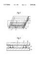
- FIG. 1is an oblique sketch of a liquid crystal cell
- FIG. 2is a cross section showing in detail section D 1 on the plane D in FIG. 1;
- FIG. 3is a reproduction of a photograph, taken using a polarising microscope (magnification 40 times) of the interface between the liquid crystal and the resin in the liquid crystal cell, prepared using the resin composition of Example 1, after standing for 500 hours at 80° C. and 90% RH, and
- FIG. 4is a reproduction of a photograph, taken using a polarising microscope (magnification 40 times), of the interface between the liquid crystal and the resin in the liquid crystal cell, prepared using the resin composition of Comparative Example 1, after standing for 15 hours at 80° C. and 90% RH.
- a liquid crystal cellcomprises transparent glass substrates 1a and 1b provided with transparent electrodes 5a and 5b, a spacer 4 to maintain the glass substrates 1a and 1b at a fixed distance apart, peripheral sealant 2 provided with liquid crystal inlet 3 and a space 6 defined by the glass substrates and spacer.
- the first step in the preparation of the liquid crystal cellwas the forming of a transparent electrode 5a, consisting for example of indium stannous oxide, on a glass substrate 1a, an oriented membrane made of polyimide resin then being formed on the transparent electrode followed by a rubbing treatment.
- a resin composition as prepared in each Example or Comparative Examplewas then applied to the peripheral parts of the glass substrate and to the inner partition (not shown in FIGS. 1 and 2) of the cell by screen printing.
- the glass plate 1awas then combined with a second glass plate 1b, to which the same treatment had been applied, and a spacer 4 of 10 microns thickness, and pressure was applied to ensure adhesion.
- the cell, so formed,was irradiated by a xenon lamp (0.1 W/cm 2 ) for 5 minutes to cure the resin.
- a liquid crystalZL 11636 manufactured by Merck & Co
- the resin composition used as peripheral sealantwas applied to encapsulate the liquid crystal inlet.
- the encapsulant compositionwas irradiated by the xenon lamp for 5 minutes to effect cure.
- part A where light passes throughis liquid crystal
- Bis peripheral sealant and structural material for the interior of the cell
- Cis encapsulant for the inlet.
- part A where light passes throughis again liquid crystal and part B is sealant/encapsulant. It is obvious from the schlieren effect that can be seen at the interface between the liquid crystal and the encapsulant that the initial uniform alignment of the liquid crystal has been disturbed by the resin composition of Comparative Example 1.
- the resin composition of Comparative Example 2was used, no disturbance of alignment at the interface between the liquid crystal and the encapsulant was observed but a leakage of liquid crystal occurred after standing at 50° C. and 90% RH for 300 hours.
- the resin composition of Comparative Example 3was used as encapsulant, a large quantity of the resin infused into the liquid crystal because of the low viscosity of the resin.
- the high viscosity resin composition of Comparative Example 4it took more than 10 minutes to obtain a proper infusion of the resin into the liquid crystal and operating difficulties were then experienced.
Landscapes
- Physics & Mathematics (AREA)
- Nonlinear Science (AREA)
- General Physics & Mathematics (AREA)
- Optics & Photonics (AREA)
- Crystallography & Structural Chemistry (AREA)
- Chemical & Material Sciences (AREA)
- Mathematical Physics (AREA)
- Spectroscopy & Molecular Physics (AREA)
- Liquid Crystal (AREA)
- Epoxy Resins (AREA)
- Compositions Of Macromolecular Compounds (AREA)
- Polymers With Sulfur, Phosphorus Or Metals In The Main Chain (AREA)
- Sealing Material Composition (AREA)
Abstract
Description
A--(SH).sub.q
Claims (4)
Applications Claiming Priority (2)
| Application Number | Priority Date | Filing Date | Title |
|---|---|---|---|
| JP6934891 | 1991-03-08 | ||
| JP3-069348 | 1991-03-08 |
Publications (1)
| Publication Number | Publication Date |
|---|---|
| US5387445Atrue US5387445A (en) | 1995-02-07 |
Family
ID=13399960
Family Applications (1)
| Application Number | Title | Priority Date | Filing Date |
|---|---|---|---|
| US07/847,170Expired - LifetimeUS5387445A (en) | 1991-03-08 | 1992-03-09 | Liquid crystal display device |
Country Status (7)
| Country | Link |
|---|---|
| US (1) | US5387445A (en) |
| EP (1) | EP0503834B1 (en) |
| JP (1) | JP3306895B2 (en) |
| AT (1) | ATE141017T1 (en) |
| DE (1) | DE69212515T2 (en) |
| DK (1) | DK0503834T3 (en) |
| ES (1) | ES2090497T3 (en) |
Cited By (43)
| Publication number | Priority date | Publication date | Assignee | Title |
|---|---|---|---|---|
| US5539545A (en)* | 1993-05-18 | 1996-07-23 | Semiconductor Energy Laboratory Co., Ltd. | Method of making LCD in which resin columns are cured and the liquid crystal is reoriented |
| US5546208A (en)* | 1993-02-19 | 1996-08-13 | Semiconductor Energy Laboratory Co., Ltd. | Electrooptical device involving a mixture of liquid crystal, photo curable resins and reaction initiating material for forming resinous columns |
| US5556670A (en)* | 1992-10-15 | 1996-09-17 | Casio Computer Co., Ltd. | Liquid crystal display panel |
| US5739882A (en)* | 1991-11-18 | 1998-04-14 | Semiconductor Energy Laboratory Co., Ltd. | LCD polymerized column spacer formed on a modified substrate, from an acrylic resin, on a surface having hydrophilic and hydrophobic portions, or at regular spacings |
| US5876805A (en)* | 1996-04-05 | 1999-03-02 | Minnesota Mining & Manufacturing Co. | Visible light polymerizable thiol-ene composition |
| US5898041A (en)* | 1995-03-01 | 1999-04-27 | Matsushita Electric Industrial Co., Ltd. | Production process of liquid crystal display panel, seal material for liquid crystal cell and liquid crystal display |
| US5991000A (en)* | 1996-06-13 | 1999-11-23 | United States Of America As Represented By The Secretary Of The Navy | Cavity uniformity having patterned spaces of aluminum oxide or silicon dioxide |
| US6001203A (en)* | 1995-03-01 | 1999-12-14 | Matsushita Electric Industrial Co., Ltd. | Production process of liquid crystal display panel, seal material for liquid crystal cell and liquid crystal display |
| US6031593A (en)* | 1996-08-23 | 2000-02-29 | Sharp Kabushiki Kaisha | Method of manufacturing spacing layer for liquid crystal display using light shielding layer as a mask |
| US6129955A (en)* | 1995-10-26 | 2000-10-10 | International Business Machines Corporation | Encapsulating a solder joint with a photo cured epoxy resin or cyanate |
| US6191841B1 (en)* | 1998-11-30 | 2001-02-20 | Kabushiki Kaisha Toshiba | Method of manufacturing liquid crystal display cell |
| US6309902B1 (en)* | 1996-08-08 | 2001-10-30 | Seiko Epson Corporation | Method for coating semiconductor element with resin, coating resin, and liquid crystal display device |
| US20020039160A1 (en)* | 2000-10-04 | 2002-04-04 | Lg Philips Lcd Co., Ltd. | Liquid crystal display device and method for manufacturing the same |
| US20030112404A1 (en)* | 2001-12-14 | 2003-06-19 | Lg.Philips Lcd Co., Ltd. | Liquid crystal display device and method of fabricating the same |
| US20030156230A1 (en)* | 2002-02-20 | 2003-08-21 | Boer Willem Den | Light sensitive display |
| US20050134749A1 (en)* | 2003-12-19 | 2005-06-23 | Adiel Abileah | Reflection resistant display |
| US20050231656A1 (en)* | 2004-04-16 | 2005-10-20 | Planar Systems, Inc. | Image sensor with photosensitive thin film transistors and dark current compensation |
| US20050249891A1 (en)* | 2000-06-21 | 2005-11-10 | Mitsui Chemicals Inc. | Sealant material for plastic liquid crystal display cells including two-component epoxy resin composition |
| US20050270438A1 (en)* | 1993-09-20 | 2005-12-08 | Semiconductor Energy Laboratory Co., Ltd. | Electro-optical device |
| US20060045240A1 (en)* | 2004-08-31 | 2006-03-02 | Buchner Gregory C | Method and apparatus for delayed answering of telecommunications request |
| US20060125971A1 (en)* | 2003-12-17 | 2006-06-15 | Planar Systems, Inc. | Integrated optical light sensitive active matrix liquid crystal display |
| US20060187367A1 (en)* | 2002-05-23 | 2006-08-24 | Adiel Abileah | Light sensitive display |
| US20070109239A1 (en)* | 2005-11-14 | 2007-05-17 | Den Boer Willem | Integrated light sensitive liquid crystal display |
| US20080048995A1 (en)* | 2003-02-20 | 2008-02-28 | Planar Systems, Inc. | Light sensitive display |
| US20080062156A1 (en)* | 2003-02-20 | 2008-03-13 | Planar Systems, Inc. | Light sensitive display |
| US20080239230A1 (en)* | 2003-03-07 | 2008-10-02 | Semiconductor Energy Laboratory Co., Ltd. | Liquid crystal display device and method for manufacturing the same |
| US20090027592A1 (en)* | 2007-07-25 | 2009-01-29 | Nec Lcd Technologies, Ltd. | Display device, manufacturing method of display device, and manufacturing apparatus for the same |
| US20090167712A1 (en)* | 2002-03-01 | 2009-07-02 | Planar Systems, Inc. | Reflection resistant touch screens |
| US8638320B2 (en) | 2011-06-22 | 2014-01-28 | Apple Inc. | Stylus orientation detection |
| US8928635B2 (en) | 2011-06-22 | 2015-01-06 | Apple Inc. | Active stylus |
| US20150048388A1 (en)* | 2013-08-16 | 2015-02-19 | Samsung Display Co., Ltd. | Flat panel display apparatus and method of manufacturing the same |
| US9176604B2 (en) | 2012-07-27 | 2015-11-03 | Apple Inc. | Stylus device |
| US9310923B2 (en) | 2010-12-03 | 2016-04-12 | Apple Inc. | Input device for touch sensitive devices |
| US9329703B2 (en) | 2011-06-22 | 2016-05-03 | Apple Inc. | Intelligent stylus |
| US20160362576A1 (en)* | 2014-02-28 | 2016-12-15 | Furukawa Electric Co., Ltd. | Resin composition for sealing electronic device, and electronic device |
| US9557845B2 (en) | 2012-07-27 | 2017-01-31 | Apple Inc. | Input device for and method of communication with capacitive devices through frequency variation |
| US9652090B2 (en) | 2012-07-27 | 2017-05-16 | Apple Inc. | Device for digital communication through capacitive coupling |
| US9939935B2 (en) | 2013-07-31 | 2018-04-10 | Apple Inc. | Scan engine for touch controller architecture |
| US10048775B2 (en) | 2013-03-14 | 2018-08-14 | Apple Inc. | Stylus detection and demodulation |
| US10061450B2 (en) | 2014-12-04 | 2018-08-28 | Apple Inc. | Coarse scan and targeted active mode scan for touch |
| US10196547B2 (en)* | 2014-02-28 | 2019-02-05 | Furukawa Electrics Co., Ltd. | Resin composition for sealing electronic device, and electronic device |
| US10474277B2 (en) | 2016-05-31 | 2019-11-12 | Apple Inc. | Position-based stylus communication |
| US12153764B1 (en) | 2020-09-25 | 2024-11-26 | Apple Inc. | Stylus with receive architecture for position determination |
Families Citing this family (9)
| Publication number | Priority date | Publication date | Assignee | Title |
|---|---|---|---|---|
| GB2279656B (en)* | 1993-06-22 | 1997-04-09 | Three Bond Co Ltd | Sealing compound for liquid crystal |
| KR0140908B1 (en)* | 1995-01-20 | 1998-06-15 | 박흥기 | Pigment dispersed photoresist composition for color filter of lcd |
| JPH1138422A (en)* | 1997-07-23 | 1999-02-12 | Sharp Corp | Liquid crystal display device and method of manufacturing the same |
| RU2172974C2 (en)* | 1999-04-20 | 2001-08-27 | ОПТИВА, Инк. | Liquid-crystal display |
| US7015990B2 (en) | 2000-04-24 | 2006-03-21 | Nitto Denko Corporation | Liquid crystal display including O-type and E-type polarizer |
| JP2003096185A (en)* | 2001-07-17 | 2003-04-03 | Mitsui Chemicals Inc | Photocurable resin composition |
| CN101535872B (en) | 2006-11-10 | 2011-12-14 | 旭硝子株式会社 | Method for manufacturing liquid crystal display and liquid crystal display |
| JP2009186962A (en)* | 2007-07-17 | 2009-08-20 | Sony Chemical & Information Device Corp | Display device manufacturing method |
| JP5831891B2 (en)* | 2011-08-10 | 2015-12-09 | デンカ株式会社 | Method for producing resin composition and adhesive |
Citations (6)
| Publication number | Priority date | Publication date | Assignee | Title |
|---|---|---|---|---|
| US3714290A (en)* | 1971-06-25 | 1973-01-30 | Grace W R & Co | Chemically curable liquid polyene-polythiol polymer composition |
| US4272586A (en)* | 1978-02-23 | 1981-06-09 | Denki Kagaku Kogyo Kabushiki Kaisha | Laminated glass product |
| US4297401A (en)* | 1978-12-26 | 1981-10-27 | Minnesota Mining & Manufacturing Company | Liquid crystal display and photopolymerizable sealant therefor |
| US4494825A (en)* | 1981-03-04 | 1985-01-22 | Hitachi, Ltd. | Fill port seal with first and second photosensitizers |
| EP0205261A2 (en)* | 1985-06-10 | 1986-12-17 | General Motors Corporation | Liquid crystal droplets dispersed in thin films of UV-curable polymers |
| WO1989006264A1 (en)* | 1987-12-28 | 1989-07-13 | Hughes Aircraft Company | Dispersion of liquid crystal droplets in a photopolymerized matrix, and devices made therefrom |
- 1992
- 1992-03-04ESES92301865Tpatent/ES2090497T3/ennot_activeExpired - Lifetime
- 1992-03-04EPEP92301865Apatent/EP0503834B1/ennot_activeExpired - Lifetime
- 1992-03-04ATAT92301865Tpatent/ATE141017T1/ennot_activeIP Right Cessation
- 1992-03-04DEDE69212515Tpatent/DE69212515T2/ennot_activeExpired - Fee Related
- 1992-03-04DKDK92301865.9Tpatent/DK0503834T3/enactive
- 1992-03-09USUS07/847,170patent/US5387445A/ennot_activeExpired - Lifetime
- 1992-03-09JPJP05089292Apatent/JP3306895B2/ennot_activeExpired - Lifetime
Patent Citations (6)
| Publication number | Priority date | Publication date | Assignee | Title |
|---|---|---|---|---|
| US3714290A (en)* | 1971-06-25 | 1973-01-30 | Grace W R & Co | Chemically curable liquid polyene-polythiol polymer composition |
| US4272586A (en)* | 1978-02-23 | 1981-06-09 | Denki Kagaku Kogyo Kabushiki Kaisha | Laminated glass product |
| US4297401A (en)* | 1978-12-26 | 1981-10-27 | Minnesota Mining & Manufacturing Company | Liquid crystal display and photopolymerizable sealant therefor |
| US4494825A (en)* | 1981-03-04 | 1985-01-22 | Hitachi, Ltd. | Fill port seal with first and second photosensitizers |
| EP0205261A2 (en)* | 1985-06-10 | 1986-12-17 | General Motors Corporation | Liquid crystal droplets dispersed in thin films of UV-curable polymers |
| WO1989006264A1 (en)* | 1987-12-28 | 1989-07-13 | Hughes Aircraft Company | Dispersion of liquid crystal droplets in a photopolymerized matrix, and devices made therefrom |
Cited By (95)
| Publication number | Priority date | Publication date | Assignee | Title |
|---|---|---|---|---|
| US5739882A (en)* | 1991-11-18 | 1998-04-14 | Semiconductor Energy Laboratory Co., Ltd. | LCD polymerized column spacer formed on a modified substrate, from an acrylic resin, on a surface having hydrophilic and hydrophobic portions, or at regular spacings |
| US5556670A (en)* | 1992-10-15 | 1996-09-17 | Casio Computer Co., Ltd. | Liquid crystal display panel |
| US5546208A (en)* | 1993-02-19 | 1996-08-13 | Semiconductor Energy Laboratory Co., Ltd. | Electrooptical device involving a mixture of liquid crystal, photo curable resins and reaction initiating material for forming resinous columns |
| US5539545A (en)* | 1993-05-18 | 1996-07-23 | Semiconductor Energy Laboratory Co., Ltd. | Method of making LCD in which resin columns are cured and the liquid crystal is reoriented |
| US7525629B2 (en)* | 1993-09-20 | 2009-04-28 | Semiconductor Energy Laboratory Co., Ltd. | Liquid crystal display device comprising drive circuits that include thin film transistors formed on both substrates |
| US20050270438A1 (en)* | 1993-09-20 | 2005-12-08 | Semiconductor Energy Laboratory Co., Ltd. | Electro-optical device |
| US5898041A (en)* | 1995-03-01 | 1999-04-27 | Matsushita Electric Industrial Co., Ltd. | Production process of liquid crystal display panel, seal material for liquid crystal cell and liquid crystal display |
| US6013339A (en)* | 1995-03-01 | 2000-01-11 | Matsushita Electric Industrial Co., Ltd. | Liquid crystal display panel, seal material for liquid crystal cell and liquid crystal display |
| US6001203A (en)* | 1995-03-01 | 1999-12-14 | Matsushita Electric Industrial Co., Ltd. | Production process of liquid crystal display panel, seal material for liquid crystal cell and liquid crystal display |
| US6129955A (en)* | 1995-10-26 | 2000-10-10 | International Business Machines Corporation | Encapsulating a solder joint with a photo cured epoxy resin or cyanate |
| US5876805A (en)* | 1996-04-05 | 1999-03-02 | Minnesota Mining & Manufacturing Co. | Visible light polymerizable thiol-ene composition |
| US5991000A (en)* | 1996-06-13 | 1999-11-23 | United States Of America As Represented By The Secretary Of The Navy | Cavity uniformity having patterned spaces of aluminum oxide or silicon dioxide |
| US6309902B1 (en)* | 1996-08-08 | 2001-10-30 | Seiko Epson Corporation | Method for coating semiconductor element with resin, coating resin, and liquid crystal display device |
| US6031593A (en)* | 1996-08-23 | 2000-02-29 | Sharp Kabushiki Kaisha | Method of manufacturing spacing layer for liquid crystal display using light shielding layer as a mask |
| US6191841B1 (en)* | 1998-11-30 | 2001-02-20 | Kabushiki Kaisha Toshiba | Method of manufacturing liquid crystal display cell |
| US20050249891A1 (en)* | 2000-06-21 | 2005-11-10 | Mitsui Chemicals Inc. | Sealant material for plastic liquid crystal display cells including two-component epoxy resin composition |
| US20020039160A1 (en)* | 2000-10-04 | 2002-04-04 | Lg Philips Lcd Co., Ltd. | Liquid crystal display device and method for manufacturing the same |
| US7429412B2 (en)* | 2000-10-04 | 2008-09-30 | Lg Display Co., Ltd. | Liquid crystal display device and method for manufacturing the same |
| US7391493B2 (en)* | 2001-12-14 | 2008-06-24 | Lg Display Lcd Co., Ltd. | Liquid crystal display device having column spacers and method of fabricating the same |
| US20030112404A1 (en)* | 2001-12-14 | 2003-06-19 | Lg.Philips Lcd Co., Ltd. | Liquid crystal display device and method of fabricating the same |
| US9134851B2 (en) | 2002-02-20 | 2015-09-15 | Apple Inc. | Light sensitive display |
| US20100059296A9 (en)* | 2002-02-20 | 2010-03-11 | Planar Systems, Inc. | Light sensitive display |
| US20050285985A1 (en)* | 2002-02-20 | 2005-12-29 | Planar Systems, Inc. | Light sensitive display |
| US7872641B2 (en) | 2002-02-20 | 2011-01-18 | Apple Inc. | Light sensitive display |
| US8570449B2 (en) | 2002-02-20 | 2013-10-29 | Apple Inc. | Light sensitive display with pressure sensor |
| US20070279346A1 (en)* | 2002-02-20 | 2007-12-06 | Planar Systems, Inc. | Display with embedded image sensor |
| US9411470B2 (en) | 2002-02-20 | 2016-08-09 | Apple Inc. | Light sensitive display with multiple data set object detection |
| US20100020044A1 (en)* | 2002-02-20 | 2010-01-28 | Apple Inc. | Light sensitive display with switchable detection modes |
| US20100013794A1 (en)* | 2002-02-20 | 2010-01-21 | Apple Inc. | Light sensitive display with multiple data set object detection |
| US20080055295A1 (en)* | 2002-02-20 | 2008-03-06 | Planar Systems, Inc. | Light sensitive display |
| US20100013793A1 (en)* | 2002-02-20 | 2010-01-21 | Apple Inc. | Light sensitive display with pressure sensor |
| US20080066972A1 (en)* | 2002-02-20 | 2008-03-20 | Planar Systems, Inc. | Light sensitive display |
| US20100013796A1 (en)* | 2002-02-20 | 2010-01-21 | Apple Inc. | Light sensitive display with object detection calibration |
| US20080111780A1 (en)* | 2002-02-20 | 2008-05-15 | Planar Systems, Inc. | Light sensitive display |
| US20080129909A1 (en)* | 2002-02-20 | 2008-06-05 | Planar Systems, Inc. | Light sensitive display |
| US20080129914A1 (en)* | 2002-02-20 | 2008-06-05 | Planar Systems, Inc. | Light sensitive display |
| US20080129913A1 (en)* | 2002-02-20 | 2008-06-05 | Planar Systems, Inc. | Light sensitive display |
| US9971456B2 (en) | 2002-02-20 | 2018-05-15 | Apple Inc. | Light sensitive display with switchable detection modes for detecting a fingerprint |
| US20030156230A1 (en)* | 2002-02-20 | 2003-08-21 | Boer Willem Den | Light sensitive display |
| US11073926B2 (en) | 2002-02-20 | 2021-07-27 | Apple Inc. | Light sensitive display |
| US8441422B2 (en) | 2002-02-20 | 2013-05-14 | Apple Inc. | Light sensitive display with object detection calibration |
| US20090167712A1 (en)* | 2002-03-01 | 2009-07-02 | Planar Systems, Inc. | Reflection resistant touch screens |
| US7852417B2 (en) | 2002-05-23 | 2010-12-14 | Apple Inc. | Light sensitive display |
| US20080165311A1 (en)* | 2002-05-23 | 2008-07-10 | Adiel Abileah | Light sensitive display |
| US8044930B2 (en) | 2002-05-23 | 2011-10-25 | Apple Inc. | Light sensitive display |
| US7880733B2 (en) | 2002-05-23 | 2011-02-01 | Apple Inc. | Light sensitive display |
| US7880819B2 (en) | 2002-05-23 | 2011-02-01 | Apple Inc. | Light sensitive display |
| US20080049153A1 (en)* | 2002-05-23 | 2008-02-28 | Adiel Abileah | Light sensitive display |
| US20080049154A1 (en)* | 2002-05-23 | 2008-02-28 | Adiel Abileah | Light sensitive display |
| US20060187367A1 (en)* | 2002-05-23 | 2006-08-24 | Adiel Abileah | Light sensitive display |
| US7830461B2 (en) | 2002-05-23 | 2010-11-09 | Apple Inc. | Light sensitive display |
| US9354735B2 (en) | 2002-05-23 | 2016-05-31 | Apple Inc. | Light sensitive display |
| US20080062156A1 (en)* | 2003-02-20 | 2008-03-13 | Planar Systems, Inc. | Light sensitive display |
| US20080048995A1 (en)* | 2003-02-20 | 2008-02-28 | Planar Systems, Inc. | Light sensitive display |
| US20080084374A1 (en)* | 2003-02-20 | 2008-04-10 | Planar Systems, Inc. | Light sensitive display |
| US8207946B2 (en) | 2003-02-20 | 2012-06-26 | Apple Inc. | Light sensitive display |
| US8634050B2 (en)* | 2003-03-07 | 2014-01-21 | Semiconductor Energy Laboratory Co., Ltd. | Liquid crystal display device and method for manufacturing the same |
| US20080239230A1 (en)* | 2003-03-07 | 2008-10-02 | Semiconductor Energy Laboratory Co., Ltd. | Liquid crystal display device and method for manufacturing the same |
| US20060125971A1 (en)* | 2003-12-17 | 2006-06-15 | Planar Systems, Inc. | Integrated optical light sensitive active matrix liquid crystal display |
| US20050134749A1 (en)* | 2003-12-19 | 2005-06-23 | Adiel Abileah | Reflection resistant display |
| US20100302419A1 (en)* | 2004-04-16 | 2010-12-02 | Apple Inc. | Image sensor with photosensitive thin film transistors and dark current compensation |
| US7773139B2 (en) | 2004-04-16 | 2010-08-10 | Apple Inc. | Image sensor with photosensitive thin film transistors |
| US20050231656A1 (en)* | 2004-04-16 | 2005-10-20 | Planar Systems, Inc. | Image sensor with photosensitive thin film transistors and dark current compensation |
| US8289429B2 (en) | 2004-04-16 | 2012-10-16 | Apple Inc. | Image sensor with photosensitive thin film transistors and dark current compensation |
| US20060045240A1 (en)* | 2004-08-31 | 2006-03-02 | Buchner Gregory C | Method and apparatus for delayed answering of telecommunications request |
| US20070109239A1 (en)* | 2005-11-14 | 2007-05-17 | Den Boer Willem | Integrated light sensitive liquid crystal display |
| US20090027592A1 (en)* | 2007-07-25 | 2009-01-29 | Nec Lcd Technologies, Ltd. | Display device, manufacturing method of display device, and manufacturing apparatus for the same |
| US9310923B2 (en) | 2010-12-03 | 2016-04-12 | Apple Inc. | Input device for touch sensitive devices |
| US9921684B2 (en) | 2011-06-22 | 2018-03-20 | Apple Inc. | Intelligent stylus |
| US8928635B2 (en) | 2011-06-22 | 2015-01-06 | Apple Inc. | Active stylus |
| US9329703B2 (en) | 2011-06-22 | 2016-05-03 | Apple Inc. | Intelligent stylus |
| US9519361B2 (en) | 2011-06-22 | 2016-12-13 | Apple Inc. | Active stylus |
| US8638320B2 (en) | 2011-06-22 | 2014-01-28 | Apple Inc. | Stylus orientation detection |
| US9176604B2 (en) | 2012-07-27 | 2015-11-03 | Apple Inc. | Stylus device |
| US9557845B2 (en) | 2012-07-27 | 2017-01-31 | Apple Inc. | Input device for and method of communication with capacitive devices through frequency variation |
| US9582105B2 (en) | 2012-07-27 | 2017-02-28 | Apple Inc. | Input device for touch sensitive devices |
| US9652090B2 (en) | 2012-07-27 | 2017-05-16 | Apple Inc. | Device for digital communication through capacitive coupling |
| US10048775B2 (en) | 2013-03-14 | 2018-08-14 | Apple Inc. | Stylus detection and demodulation |
| US11687192B2 (en) | 2013-07-31 | 2023-06-27 | Apple Inc. | Touch controller architecture |
| US9939935B2 (en) | 2013-07-31 | 2018-04-10 | Apple Inc. | Scan engine for touch controller architecture |
| US10067580B2 (en) | 2013-07-31 | 2018-09-04 | Apple Inc. | Active stylus for use with touch controller architecture |
| US12340048B2 (en) | 2013-07-31 | 2025-06-24 | Apple Inc. | Touch controller architecture |
| US10845901B2 (en) | 2013-07-31 | 2020-11-24 | Apple Inc. | Touch controller architecture |
| US20150048388A1 (en)* | 2013-08-16 | 2015-02-19 | Samsung Display Co., Ltd. | Flat panel display apparatus and method of manufacturing the same |
| US8969888B1 (en)* | 2013-08-16 | 2015-03-03 | Samsung Display Co., Ltd. | Flat panel display apparatus and method of manufacturing the same |
| US10196547B2 (en)* | 2014-02-28 | 2019-02-05 | Furukawa Electrics Co., Ltd. | Resin composition for sealing electronic device, and electronic device |
| US10196534B2 (en)* | 2014-02-28 | 2019-02-05 | Furukawa Electric Co., Ltd. | Resin composition for sealing electronic device, and electronic device |
| TWI634148B (en)* | 2014-02-28 | 2018-09-01 | 古河電氣工業股份有限公司 | Resin composition for electronic device sealing and electronic device |
| US20160362576A1 (en)* | 2014-02-28 | 2016-12-15 | Furukawa Electric Co., Ltd. | Resin composition for sealing electronic device, and electronic device |
| US10067618B2 (en) | 2014-12-04 | 2018-09-04 | Apple Inc. | Coarse scan and targeted active mode scan for touch |
| US10664113B2 (en) | 2014-12-04 | 2020-05-26 | Apple Inc. | Coarse scan and targeted active mode scan for touch and stylus |
| US10061449B2 (en) | 2014-12-04 | 2018-08-28 | Apple Inc. | Coarse scan and targeted active mode scan for touch and stylus |
| US10061450B2 (en) | 2014-12-04 | 2018-08-28 | Apple Inc. | Coarse scan and targeted active mode scan for touch |
| US10474277B2 (en) | 2016-05-31 | 2019-11-12 | Apple Inc. | Position-based stylus communication |
| US12153764B1 (en) | 2020-09-25 | 2024-11-26 | Apple Inc. | Stylus with receive architecture for position determination |
Also Published As
| Publication number | Publication date |
|---|---|
| JPH06220305A (en) | 1994-08-09 |
| DE69212515T2 (en) | 1996-12-05 |
| ES2090497T3 (en) | 1996-10-16 |
| ATE141017T1 (en) | 1996-08-15 |
| DK0503834T3 (en) | 1996-08-26 |
| EP0503834A3 (en) | 1992-10-07 |
| EP0503834B1 (en) | 1996-07-31 |
| EP0503834A2 (en) | 1992-09-16 |
| JP3306895B2 (en) | 2002-07-24 |
| DE69212515D1 (en) | 1996-09-05 |
Similar Documents
| Publication | Publication Date | Title |
|---|---|---|
| US5387445A (en) | Liquid crystal display device | |
| JP4211942B2 (en) | Liquid crystal sealant and liquid crystal display cell using the same | |
| TWI420205B (en) | Hardening resin composition for liquid crystal sealing and manufacturing method for liquid crystal display panel using the same | |
| CN102804045B (en) | Visible light-curable liquid crystal sealing material and liquid crystal display cell using same | |
| WO2012011220A1 (en) | Liquid crystal sealing agent and liquid crystal display cell using same | |
| JP2007316624A (en) | Sealing material for liquid crystal dispensing method, vertically conducting material, and liquid crystal display device | |
| JP4948317B2 (en) | Liquid crystal sealant, liquid crystal display panel manufacturing method using the same, and liquid crystal display panel | |
| JP7421691B1 (en) | Sealant for liquid crystal display elements and liquid crystal display elements | |
| CN103635854B (en) | Liquid crystal sealing agent and use its liquid crystal display | |
| JPH0713173A (en) | Sealing agent for liquid crystal | |
| JP7112604B1 (en) | Liquid crystal display element sealant, vertical conduction material, and liquid crystal display element | |
| JP2020042089A (en) | Sealant for liquid crystal display element, vertical conductive material, and liquid crystal display element | |
| JP7253118B1 (en) | Sealant for liquid crystal display element and liquid crystal display element | |
| JP6849866B1 (en) | Curable resin composition, sealant for liquid crystal display element, vertical conductive material, and liquid crystal display element | |
| CN112424680B (en) | Light-shielding sealant for liquid crystal instillation process and method for manufacturing liquid crystal display panel using same | |
| JP2006039096A (en) | Composition for liquid crystal display device | |
| JP7007524B1 (en) | Sealing agent for liquid crystal display element, vertical conduction material, and liquid crystal display element | |
| JP6922114B1 (en) | Sealant for display element, vertical conduction material and display element | |
| JP2006023581A (en) | Curable resin composition for liquid crystal display element | |
| KR20180094594A (en) | Sealant composition for liquid crystal display device | |
| CN120722615A (en) | Method for producing liquid crystal sealing agent for liquid crystal instillation method and method for producing liquid crystal display panel | |
| JP2024068730A (en) | Liquid crystal sealant for liquid crystal dropping method and liquid crystal display cell using same | |
| JP2025130705A (en) | Sealant for optical devices | |
| CN120020193A (en) | Liquid crystal sealant for liquid crystal dropping method and liquid crystal display panel using the same | |
| JP2023083652A (en) | Liquid crystal sealant for liquid crystal dropping method and liquid crystal display panel using the same |
Legal Events
| Date | Code | Title | Description |
|---|---|---|---|
| AS | Assignment | Owner name:IMPERIAL CHEMICAL INDUSTRIES PLC, ENGLAND Free format text:ASSIGNMENT OF ASSIGNORS INTEREST.;ASSIGNORS:HORIUCHI, SHIN;WAKABAYASHI, SUMIO;DOBA, TAKAHISA;REEL/FRAME:006129/0268 Effective date:19920317 | |
| AS | Assignment | Owner name:ZENECA LIMITED, ENGLAND Free format text:ASSIGNMENT OF ASSIGNORS INTEREST;ASSIGNOR:IMPERIAL CHEMICAL INDUSTRIES PLC;REEL/FRAME:006965/0039 Effective date:19931102 | |
| STCF | Information on status: patent grant | Free format text:PATENTED CASE | |
| AS | Assignment | Owner name:ABLESTIK LABORATORIES Free format text:ASSIGNMENT OF ASSIGNORS INTEREST;ASSIGNOR:ZENECA LIMITED;REEL/FRAME:007404/0043 Effective date:19940922 | |
| AS | Assignment | Owner name:NATIONAL STARCH AND CHEMICAL INVESTMENT HOLDING CO Free format text:ASSIGNMENT OF ASSIGNORS INTEREST;ASSIGNOR:ABLESTIK LABORATORIES;REEL/FRAME:007543/0653 Effective date:19950315 | |
| FEPP | Fee payment procedure | Free format text:PAYOR NUMBER ASSIGNED (ORIGINAL EVENT CODE: ASPN); ENTITY STATUS OF PATENT OWNER: LARGE ENTITY | |
| FPAY | Fee payment | Year of fee payment:4 | |
| FPAY | Fee payment | Year of fee payment:8 | |
| FPAY | Fee payment | Year of fee payment:12 | |
| AS | Assignment | Owner name:HENKEL CORPORATION, CONNECTICUT Free format text:MERGER;ASSIGNOR:NATIONAL STARCH AND CHEMICAL INVESTMENT AND HOLDING CORPORATION;REEL/FRAME:025095/0884 Effective date:20081231 |