US5387314A - Fabrication of ink fill slots in thermal ink-jet printheads utilizing chemical micromachining - Google Patents
Fabrication of ink fill slots in thermal ink-jet printheads utilizing chemical micromachiningDownload PDFInfo
- Publication number
- US5387314A US5387314AUS08/009,151US915193AUS5387314AUS 5387314 AUS5387314 AUS 5387314AUS 915193 AUS915193 AUS 915193AUS 5387314 AUS5387314 AUS 5387314A
- Authority
- US
- United States
- Prior art keywords
- ink
- fill slot
- ink fill
- feed channel
- etching
- Prior art date
- Legal status (The legal status is an assumption and is not a legal conclusion. Google has not performed a legal analysis and makes no representation as to the accuracy of the status listed.)
- Expired - Lifetime
Links
- 238000005459micromachiningMethods0.000titleclaimsdescription8
- 238000004519manufacturing processMethods0.000titledescription7
- 239000000126substanceSubstances0.000titledescription2
- 238000000034methodMethods0.000claimsabstractdescription44
- 239000000758substrateSubstances0.000claimsabstractdescription33
- 238000005299abrasionMethods0.000claimsabstractdescription6
- 238000003754machiningMethods0.000claimsabstractdescription6
- 238000001020plasma etchingMethods0.000claimsabstractdescription6
- 238000000608laser ablationMethods0.000claimsabstractdescription3
- 238000005530etchingMethods0.000claimsdescription27
- XUIMIQQOPSSXEZ-UHFFFAOYSA-NSiliconChemical compound[Si]XUIMIQQOPSSXEZ-UHFFFAOYSA-N0.000claimsdescription23
- 229910052710siliconInorganic materials0.000claimsdescription22
- 239000010703siliconSubstances0.000claimsdescription22
- 230000004888barrier functionEffects0.000claimsdescription18
- 238000000059patterningMethods0.000claimsdescription3
- 238000005488sandblastingMethods0.000claimsdescription2
- 239000010409thin filmSubstances0.000claims3
- 239000003989dielectric materialSubstances0.000claims2
- 238000003631wet chemical etchingMethods0.000claims1
- 239000012530fluidSubstances0.000abstractdescription10
- 239000000463materialSubstances0.000abstractdescription5
- 238000003486chemical etchingMethods0.000abstractdescription4
- 238000010304firingMethods0.000description14
- 230000008569processEffects0.000description14
- 235000012431wafersNutrition0.000description10
- 230000000873masking effectEffects0.000description5
- 238000007639printingMethods0.000description5
- 230000008901benefitEffects0.000description4
- 230000015572biosynthetic processEffects0.000description3
- 238000007641inkjet printingMethods0.000description3
- VYPSYNLAJGMNEJ-UHFFFAOYSA-NSilicium dioxideChemical compoundO=[Si]=OVYPSYNLAJGMNEJ-UHFFFAOYSA-N0.000description2
- 238000013016dampingMethods0.000description2
- 238000001035dryingMethods0.000description2
- 238000010438heat treatmentMethods0.000description2
- 230000006872improvementEffects0.000description2
- 238000004377microelectronicMethods0.000description2
- 230000004048modificationEffects0.000description2
- 238000012986modificationMethods0.000description2
- 230000004044responseEffects0.000description2
- 229910052581Si3N4Inorganic materials0.000description1
- 230000009471actionEffects0.000description1
- 239000000654additiveSubstances0.000description1
- 230000000996additive effectEffects0.000description1
- 239000007864aqueous solutionSubstances0.000description1
- 230000009286beneficial effectEffects0.000description1
- 238000006243chemical reactionMethods0.000description1
- 150000001875compoundsChemical class0.000description1
- 239000004020conductorSubstances0.000description1
- 239000013078crystalSubstances0.000description1
- 230000007423decreaseEffects0.000description1
- 230000001419dependent effectEffects0.000description1
- 238000001312dry etchingMethods0.000description1
- 230000000694effectsEffects0.000description1
- NBVXSUQYWXRMNV-UHFFFAOYSA-NfluoromethaneChemical compoundFCNBVXSUQYWXRMNV-UHFFFAOYSA-N0.000description1
- 230000005499meniscusEffects0.000description1
- 239000000203mixtureSubstances0.000description1
- 229910021421monocrystalline siliconInorganic materials0.000description1
- 229910052756noble gasInorganic materials0.000description1
- 150000002835noble gasesChemical class0.000description1
- 230000010355oscillationEffects0.000description1
- 238000002161passivationMethods0.000description1
- 229920002120photoresistant polymerPolymers0.000description1
- 235000012239silicon dioxideNutrition0.000description1
- 239000000377silicon dioxideSubstances0.000description1
- HQVNEWCFYHHQES-UHFFFAOYSA-Nsilicon nitrideChemical compoundN12[Si]34N5[Si]62N3[Si]51N64HQVNEWCFYHHQES-UHFFFAOYSA-N0.000description1
Images


Classifications
- B—PERFORMING OPERATIONS; TRANSPORTING
- B41—PRINTING; LINING MACHINES; TYPEWRITERS; STAMPS
- B41J—TYPEWRITERS; SELECTIVE PRINTING MECHANISMS, i.e. MECHANISMS PRINTING OTHERWISE THAN FROM A FORME; CORRECTION OF TYPOGRAPHICAL ERRORS
- B41J2/00—Typewriters or selective printing mechanisms characterised by the printing or marking process for which they are designed
- B41J2/005—Typewriters or selective printing mechanisms characterised by the printing or marking process for which they are designed characterised by bringing liquid or particles selectively into contact with a printing material
- B41J2/01—Ink jet
- B41J2/135—Nozzles
- B41J2/14—Structure thereof only for on-demand ink jet heads
- B41J2/14016—Structure of bubble jet print heads
- B41J2/14032—Structure of the pressure chamber
- B41J2/1404—Geometrical characteristics
- B—PERFORMING OPERATIONS; TRANSPORTING
- B41—PRINTING; LINING MACHINES; TYPEWRITERS; STAMPS
- B41J—TYPEWRITERS; SELECTIVE PRINTING MECHANISMS, i.e. MECHANISMS PRINTING OTHERWISE THAN FROM A FORME; CORRECTION OF TYPOGRAPHICAL ERRORS
- B41J2/00—Typewriters or selective printing mechanisms characterised by the printing or marking process for which they are designed
- B41J2/005—Typewriters or selective printing mechanisms characterised by the printing or marking process for which they are designed characterised by bringing liquid or particles selectively into contact with a printing material
- B41J2/01—Ink jet
- B41J2/135—Nozzles
- B41J2/14—Structure thereof only for on-demand ink jet heads
- B41J2/14016—Structure of bubble jet print heads
- B41J2/14145—Structure of the manifold
- B—PERFORMING OPERATIONS; TRANSPORTING
- B41—PRINTING; LINING MACHINES; TYPEWRITERS; STAMPS
- B41J—TYPEWRITERS; SELECTIVE PRINTING MECHANISMS, i.e. MECHANISMS PRINTING OTHERWISE THAN FROM A FORME; CORRECTION OF TYPOGRAPHICAL ERRORS
- B41J2/00—Typewriters or selective printing mechanisms characterised by the printing or marking process for which they are designed
- B41J2/005—Typewriters or selective printing mechanisms characterised by the printing or marking process for which they are designed characterised by bringing liquid or particles selectively into contact with a printing material
- B41J2/01—Ink jet
- B41J2/135—Nozzles
- B41J2/16—Production of nozzles
- B41J2/1601—Production of bubble jet print heads
- B41J2/1603—Production of bubble jet print heads of the front shooter type
- B—PERFORMING OPERATIONS; TRANSPORTING
- B41—PRINTING; LINING MACHINES; TYPEWRITERS; STAMPS
- B41J—TYPEWRITERS; SELECTIVE PRINTING MECHANISMS, i.e. MECHANISMS PRINTING OTHERWISE THAN FROM A FORME; CORRECTION OF TYPOGRAPHICAL ERRORS
- B41J2/00—Typewriters or selective printing mechanisms characterised by the printing or marking process for which they are designed
- B41J2/005—Typewriters or selective printing mechanisms characterised by the printing or marking process for which they are designed characterised by bringing liquid or particles selectively into contact with a printing material
- B41J2/01—Ink jet
- B41J2/135—Nozzles
- B41J2/16—Production of nozzles
- B41J2/1621—Manufacturing processes
- B41J2/1626—Manufacturing processes etching
- B41J2/1628—Manufacturing processes etching dry etching
- B—PERFORMING OPERATIONS; TRANSPORTING
- B41—PRINTING; LINING MACHINES; TYPEWRITERS; STAMPS
- B41J—TYPEWRITERS; SELECTIVE PRINTING MECHANISMS, i.e. MECHANISMS PRINTING OTHERWISE THAN FROM A FORME; CORRECTION OF TYPOGRAPHICAL ERRORS
- B41J2/00—Typewriters or selective printing mechanisms characterised by the printing or marking process for which they are designed
- B41J2/005—Typewriters or selective printing mechanisms characterised by the printing or marking process for which they are designed characterised by bringing liquid or particles selectively into contact with a printing material
- B41J2/01—Ink jet
- B41J2/135—Nozzles
- B41J2/16—Production of nozzles
- B41J2/1621—Manufacturing processes
- B41J2/1626—Manufacturing processes etching
- B41J2/1629—Manufacturing processes etching wet etching
- B—PERFORMING OPERATIONS; TRANSPORTING
- B41—PRINTING; LINING MACHINES; TYPEWRITERS; STAMPS
- B41J—TYPEWRITERS; SELECTIVE PRINTING MECHANISMS, i.e. MECHANISMS PRINTING OTHERWISE THAN FROM A FORME; CORRECTION OF TYPOGRAPHICAL ERRORS
- B41J2/00—Typewriters or selective printing mechanisms characterised by the printing or marking process for which they are designed
- B41J2/005—Typewriters or selective printing mechanisms characterised by the printing or marking process for which they are designed characterised by bringing liquid or particles selectively into contact with a printing material
- B41J2/01—Ink jet
- B41J2/135—Nozzles
- B41J2/16—Production of nozzles
- B41J2/1621—Manufacturing processes
- B41J2/1631—Manufacturing processes photolithography
- B—PERFORMING OPERATIONS; TRANSPORTING
- B41—PRINTING; LINING MACHINES; TYPEWRITERS; STAMPS
- B41J—TYPEWRITERS; SELECTIVE PRINTING MECHANISMS, i.e. MECHANISMS PRINTING OTHERWISE THAN FROM A FORME; CORRECTION OF TYPOGRAPHICAL ERRORS
- B41J2/00—Typewriters or selective printing mechanisms characterised by the printing or marking process for which they are designed
- B41J2/005—Typewriters or selective printing mechanisms characterised by the printing or marking process for which they are designed characterised by bringing liquid or particles selectively into contact with a printing material
- B41J2/01—Ink jet
- B41J2/135—Nozzles
- B41J2/16—Production of nozzles
- B41J2/1621—Manufacturing processes
- B41J2/1632—Manufacturing processes machining
- B41J2/1634—Manufacturing processes machining laser machining
Definitions
- the present applicationis related to U.S. Pat. No. 5,317,346, entitled “Compound Ink Feed Slot” and assigned to the same assignee as the present application.
- the present applicationis also related to U.S. Pat. No. 5,308,442, entitled “Anisotropically Etched Ink Feed Slot in Silicon” and assigned to the same assignee as the present application.
- the present inventionrelates to thermal ink-jet printers, and, more particularly, to an improved printhead structure for introducing ink into the firing chambers.
- the art of thermal ink-jet printingit is known to provide a plurality of electrically resistive elements on a common substrate for the purpose of heating a corresponding plurality of ink volumes contained in adjacent ink reservoirs leading to the ink ejection and printing process.
- the adjacent ink reservoirsare typically provided as cavities in a barrier layer attached to the substrate for properly isolating mechanical energy to predefined volumes of ink.
- the mechanical energyresults from the conversion of electrical energy supplied to the resistive elements which creates a rapidly expanding vapor bubble in the ink above the resistive elements.
- a plurality of ink ejection orificesare provided above these cavities in a nozzle plate and provide exit paths for ink during the printing process.
- thermal ink-jet printheadsit is necessary to provide a flow of ink to the thermal, or resistive, element causing ink drop ejection. This has been accomplished by manufacturing ink fill channels, or slots, in the substrate, ink barrier, or nozzle plate.
- U.S. Pat. No. 4,789,425is directed to the "roof-shooter" configuration.
- this patentemploys anisotropic etching of the substrate to form ink feed channels, it fails to address the issue of how to supply the volume of ink required at higher frequencies of operation.
- control of geometry, pen speed, or specific hydraulic damping controlfails to address the issue of precisely matching the fluid impedance of every functional nozzle so that they all behave the same.
- an ink fill slotcan be precisely manufactured in a substrate utilizing photolithographic techniques with chemical etching, plasma etching, or a combination thereof. These methods may be used in conjunction with laser machining, mechanical abrasion, electromechanical machining, or conventional etch to remove additional substrate material in desired areas.
- the improved ink-jet printhead of the inventionincludes a plurality of ink-propelling thermal elements, each ink-propelling element disposed in a separate drop ejection chamber defined by three barrier walls and a fourth side open to a reservoir of ink common to at least some of the elements, and a plurality of nozzles comprising orifices disposed in a cover plate in close proximity to the elements, each orifice operatively associated with an element for ejecting a quantity of ink normal to the plane defined by each element and through the orifices toward a print medium in pre-defined sequences to form alphanumeric characters and graphics thereon.
- Inkis supplied to the thermal element from an ink fill slot by means of an ink feed channel.
- Each drop ejection chambermay be provided with a pair of opposed projections formed in walls in the ink feed channel and separated by a width to cause a constriction between the plenum and the channel, and each drop ejection chamber may be further provided with lead-in lobes disposed between the projections and separating one ink feed channel from a neighboring ink feed channel.
- the improvementcomprises forming the ink fill slot and the drop ejection chamber and associated ink feed channel on one substrate, in which the ink fill slot is partially formed by anisotropic etching of the substrate, employing chemical and/or plasma etching.
- the dimensions of the ink fill slot relative to the ink feed channelmay be precisely controlled to aid in fluid tuning of the pen.
- the ink fill slot positioncan be controlled to within about 20 ⁇ m of the hydraulic limiting orifice (the area between the lead-in lobes) and can be modulated in depth as the slot extends to minimize air bubble trapping.
- the frequency of operation of thermal ink-jet pensis dependent upon the shelf or distance the ink needs to travel from the ink fill slot to the firing chamber, among other things. At higher frequencies, this distance, or shelf, must also be fairly tightly controlled. Through photochemical micromachining, this distance can be more tightly controlled and placed closer to the firing chamber. Etching can be from the frontside, backside, or both. A combination of etch processes can allow a range of profiles of the ink fill slot and shelf. This process can be used instead of, or in conjunction with, conventional "mechanical" slotting procedures to enhance performance or allow batch processing.
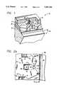
- FIG. 1is a perspective view of a resistor situated in a firing chamber formed from a barrier layer, an ink feed channel fluidically communicating with the firing chamber, and an ink fill slot for supplying ink to the ink feed channel, in accordance with the invention
- FIG. 2ais a top plan view of the configuration depicted in FIG. 1 and including adjacent resistors and ink feed channels, in which the shelf length is a constant dimension as measured from the entrance to the ink feed channel;
- FIG. 2bis a view similar to that of FIG. 2a, but depicting an equalized shelf length that follows the contours of the barrier layer;
- FIG. 3is a top plan view of a portion of a printhead, showing one embodiment of a plurality of the configurations depicted in FIG. 2A;
- FIGS. 4A-4Dare cross-sectional view of the resistor configuration of FIG. 3, showing the results of anisotropic etching of a ⁇ 100> oriented silicon substrate;
- FIG. 5A-5Dare a similar views as FIGS. 4A-4D, but with a ⁇ 110> oriented silicon substrate;
- FIG. 6A-6Dare cross-sectional view equivalent to FIGS. 4A-4D or 5A-5D in which the ink-feed slot is produced by abrasive or laser micromachining;
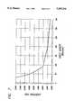
- FIG. 7on coordinates of pen frequency in Hertz and shelf length in micrometers, is a plot of the dependence of pen frequency as a function of shelf length for a specific drop volume case.
- FIG. 1depicts a printing or drop ejecting element 10, formed on a substrate 12.
- FIGS. 2a and 2bdepict three adjacent printing elements 10, while FIG. 3 depicts a portion of a printhead 13 comprising a plurality of such firing elements and shows a common ink fill slot 18 providing a supply of ink thereto.
- FIG. 3depicts one common configuration of a plurality of firing elements, namely, two parallel rows of the firing elements 10 about a common ink fill slot 18, other configurations employed in thermal ink-jet printing, such as approximately circular and single row, may also be formed in the practice of the invention.
- Each firing element 10comprises an ink feed channel 14, with a resistor 16 situated at one end 14a thereof.
- the ink feed channel 14 and drop ejection chamber 15 encompassing the resistor 16 on three sidesare formed in a layer 17 which comprises a photopolymerizable material which is appropriately masked and etched/developed to form the desired patterned opening.
- Ink(not shown) is introduced at the opposite end 14b of the ink feed channel 14, as indicated by arrow "A", from an ink fill slot, indicated generally at 18.
- a pair of opposed projections 24 at the entrance to the ink feed channel 14provide a localized constriction, as indicated by the arrow "B".
- the purpose of the localized constrictionwhich is related to improve the damping of fluid motion of the ink, is more specifically described in U.S. Pat. No. 4,882,595, and forms no part of this invention.
- Each such printing element 10comprises the various features set forth above.
- Each resistor 16is seen to be set in a drop ejection chamber 15 defined by three barrier walls and a fourth side open to the ink fill slot 18 of ink common to at least some of the elements 10, with a plurality of nozzles 20 comprising orifices disposed in a cover plate 22 near the resistors 16.
- Each orifice 20is thus seen to be operatively associated with an resistor 16 for ejecting a quantity of ink normal to the plane defined by that resistor and through the orifices toward a print medium (not shown) in defined patterns to form alphanumeric characters and graphics thereon.
- Each firing element 10is provided with a pair of opposed projections 24 formed in walls in the ink feed channel 14 and separated by a width "B" to cause a constriction between the ink fill slot 18 and the channel.
- Each firing element 10may be provided with lead-in lobes 24a disposed between the projections 24 and separating one ink feed channel 14 from a neighboring ink feed channel 14'.
- the improvementcomprises a precision means of forming the ink fill slot 18 and associated ink feed channel 14 on one substrate 12.
- the ink fill slot 18is extended to the pair of lead-in lobes 24a of each firing chamber, either at a constant distance from the entrance to the ink feed channel 14, as shown in FIG. 2A, or at an equalized distance from the contour formed by the barrier layer 17, as shown in FIG. 2B.
- the ink fill slot 18is extended by means of extension 18a toward the lead-in lobes 24a, using precise etching, described in greater detail below, to controllably align the ink fill slot relative to the entrance to the ink feed channel 14, indicated at "A".
- the extended portion 18a of the ink fill slot 18terminates at a constant distance from the centerline of the ink fill slot, very close to the lead-in lobes 24a.
- Use of precise etching, described below,permits a shorter shelf length, S L , to be formed; this shelf length is shorter than that of a presently commercially available pen used in Hewlett-Packard's DeskJet® printer, which extends to the edge of the ink fill slot 18.
- the shorter shelf lengthpermits firing at higher frequencies than presently commercially available pens. While the fluid impedance of the pen imparted to the ink is reduced compared to that in the commercially available pens, thereby resulting in improved performance, it is not substantially constant from one resistor heater 16 to the next.
- the extended portion 18a of the ink fill slot 18follows the contour of the barrier wall 17 defining the lead-in lobes 24a, providing an equalized shelf length S L .
- This equalized shelf lengthprovides a substantially constant fluid impedance to the ink in the pen, which results in improved pen performance.
- the extended portion 18a of the ink fill slot 18is precisely manufactured in a substrate 12 utilizing photolithographic techniques with chemical etching, plasma etching, or a combination thereof. These methods may be used in conjunction with laser micromachining, mechanical abrasion, or electromechanical machining to remove additional substrate material in desired areas.
- Representative substrates for the fabrication of ink fill slots 18 in accordance with the inventioncomprise single crystal silicon wafers, commonly used in the microelectronics industry. Silicon wafers with ⁇ 100> or ⁇ 110> crystal orientations are preferred. Three methods of ink fill slot fabrication consistent with this invention are detailed below. Typical resultant structures are shown in FIGS. 4C, 5C, and 6C.
- Thermally grown oxide 26is a representative etch mask for silicon.
- the barrier layer 17 and defined drop ejection chamber 15 and ink feed channel 14, along with resistor heater 16 and associated electrical traces,are formed in separate steps prior to this step.
- the etching in this stepmay be done using any or all of an isotropic etchant, such as dry (plasma) etching.
- FIG. 4Dis a cross-sectional view of a final structure in which ink is fed from the bottom of the substrate 12.
- ⁇ 100> oriented siliconis employed as the substrate 12.
- An oxide film 26, preferably silicon dioxide,is formed on both surfaces 12a, 12b of the substrate and is used to define the ink fill slot 18 to be etched.
- a silicon nitride film or other masking layercould be used, as detailed in the prior art.
- the dielectric 26 on the secondary surface 12bis patterned prior to formation of the ink fill slot 18.
- the ink fill slot 18comprises two portions.
- the first portion, 18'is formed by anisotropic etching. Since the anisotropic etching is in ⁇ 100> silicon, the angle formed is 54.74° , as is well-known.
- An aqueous solution of KOH, in a ratio of KOH:H 2 O of 2:1, heated to about 85° C.is used for the anisotropic etching.
- This etchantetches ⁇ 100> silicon at a rate of about 1.6 ⁇ m/minute.
- the etching actionis greatly reduced at a point where the ⁇ 111>planes intersect, and the ⁇ 100> bottom surface no longer exists.
- the anisotropic etchingis stopped part way through the silicon wafer 12, as shown in FIG. 4A.
- heater resistors 16and electrical traces, or conductors, associated therewith, not shown are formed on the front surface 12a of the wafer, as shown in FIG. 4B.
- the processwhich is well-known, comprises forming appropriate layers and patterning them.
- the second portion, 18a, of the ink fill slot 18is formed by a combination of isotropic and anisotropic etching, either by wet or dry processes, from the primary surface 12'. This process etches through the dielectric layer 26 on the primary surface 12a and into the silicon wafer 12 to connect with the previously-etched ink fill slot portion 18'.
- the resulting structureis shown in FIG. 4C.
- Dry etching in a plasma systemmay be used to define the second portion 18a.
- CF 4may be used, but other plasma etchants are also available for faster etching of the passivation while still protecting the silicon surface from overetch.
- etching stepbrings the ink fill slot 18 very close to the ink feed channel 14.
- the proximity of the ink fill slot 18 to the ink feed channel 14permits the printhead to be very responsive to demands for ink required at high drop ejection frequencies.
- Suitable maskingis used to form the second portion 18a; this masking may be configured to permit obtaining either the constant shelf length structure depicted in FIG. 2A or the equalized shelf length structure depicted in FIG. 2B.
- the structureis completed, as depicted in FIG. 4D, by the formation of the barrier layer 17 and the orifice plate 22 with nozzles 20 therein.
- FIGS. 5A-Drepresent a similar cross-sectional view of a final structure in which ink is fed from the bottom of the substrate 12, which in this case is ⁇ 110> oriented.
- anisotropic etchingmay be used to etch part way or all the way through the substrate 10, using the same etchant as for ⁇ 100>.
- the only difference in the process of this embodiment from that depicted in FIGS. 4A-Dis the use of silicon of a different crystallographic orientation.
- the waferis processed by known thermal ink-jet processes on the primary surface to form resistors 16 on the surface of the passivating layer 26.
- a suitable photodefined masking layer(not shown) is then applied and imaged, exposing the area to be precision etched.
- masking layersinclude DuPont's VACREL and positive or negative photoresists, such as Hoechst AZ4906 or OCG SC900, respectively.
- only the primary surface, 12aneeds to be protected by the in-sulating dielectric layer 26.
- Etchingis done by well-documented dry processes utilizing CF 4 +O 2 , SF 6 , or a mixture of fluorocarbon and noble gases to form portion 18a.
- the etch profilecan be controlled by varying operating pressure and/or etcher configuration from reactive ion etching regimes (about 50 to 150 millitort pressures and about 400 to 1,000 volts effective bias) anisotropic etching to high pressure planar etch regions (about 340 to 700 millitorr pressure and 0 to about 100 volts effective bias) isotropic etching or some subtle and beneficial combination of processes.
- the main part 18' of the ink feed slot 18is then formed by micromachining, such as mechanical abrasion, e.g., sandblasting, or laser ablation, or electromechanical machining from the secondary surface 12b.
- the barrier layer 17is generally formed prior to the final formation of the main part 18', for reasons related to wafer handling (making the wafer stronger) and parts flow (avoiding returning the wafer to the clean room for processing).
- the frequency limit of a thermal ink-jet penis limited by resistance in the flow of ink to the nozzle. Some resistance in ink flow is necessary to damp meniscus oscillation. However, too much resistance limits the upper frequency that a pen can operate.
- Ink flow resistanceis intentionally controlled by a gap adjacent the resistor 16 with a well-defined length and width. This gap is the ink feed channel 14, and its geometry is described elsewhere; see, e.g., U.S. Pat. No. 4,882,595, issued to K. E. Trueba et al and assigned to the same assignee as the present application.
- the distance of the resistor 16 from the ink fill slot 18varies with the firing patterns of the printhead.
- the entrancecomprises a region between the orifice plate 22 and the substrate 12 and its height is essentially a function of the thickness of the barrier material 17. This region has high impedance, since its height is small, and is additive to the well-controlled intentional impedance of the gap adjacent the resistor.
- the distance from the ink fill slot 18 to the entrance to the ink feed channel 14is designated the shelf S L .
- the effect of the length of the shelf on pen frequencycan be seen in FIG. 7: as the shelf increases in length, the nozzle frequency decreases.
- the substrate 12is etchedin this shelf region to form extension 18a of the ink fill slot 18, which effectively reduces the shelf length and increases the cross-sectional area of the entrance to the ink feed channel 14.
- the fluid impedanceis reduced; both of the embodiments described above are so treated. In this manner, all nozzles have a more uniform frequency response.
- the advantage of the process of the inventionis that the entire pen can now operate at a uniform higher frequency.
- each nozzle 20had a different impedance as a function of its shelf length. With this variable eliminated, all nozzles have substantially the same impedance, thus tuning is simplified and when one nozzle is optimized, all nozzles are optimized.
- the penhad to be tuned for worst case nozzles, that is, the gap had to be tightened so that the nozzles lowest in impedance (shortest shelf) were not under-damped. Therefore, nozzles with a larger shelf would have greater impedance and lower frequency response.
- the curve shown in FIG. 7has been derived from a pen ejecting droplets of about 130 pl volume.
- a shelf length of about 10 to 50 ⁇ mis preferred for high operating frequency.
- the curvesare flatter and faster.
- FIGS. 2A and 2Bdepict the shelf length (S L ).
- the shelfis at a constant location on the die and therefore the S L dimension as measured from the entrance to the ink feed channel 14 varies somewhat due to resistor stagger, while in the latter case, the shelf length is equalized, in that it follows the contours of the barrier layer 17.
- the precision etch of the primary surface of the silicon substrate in combination with the anisotropically etch through the secondary surfaceprovides improved ink flow characteristics and is expected to find use in thermal ink-jet printheads.
- the precision etchmay be done by a variety of isotropic etching processes.
Landscapes
- Engineering & Computer Science (AREA)
- Manufacturing & Machinery (AREA)
- Physics & Mathematics (AREA)
- Geometry (AREA)
- Optics & Photonics (AREA)
- Particle Formation And Scattering Control In Inkjet Printers (AREA)
Abstract
Description
Claims (18)
Priority Applications (6)
| Application Number | Priority Date | Filing Date | Title |
|---|---|---|---|
| US08/009,151US5387314A (en) | 1993-01-25 | 1993-01-25 | Fabrication of ink fill slots in thermal ink-jet printheads utilizing chemical micromachining |
| DE69403352TDE69403352T2 (en) | 1993-01-25 | 1994-01-19 | Process for manufacturing a thermal ink jet print head |
| EP94300395AEP0609012B1 (en) | 1993-01-25 | 1994-01-19 | Method for manufacturing a thermal ink-jet print head |
| JP02327494AJP3535557B2 (en) | 1993-01-25 | 1994-01-25 | Method of forming ink-filled slot in inkjet printhead |
| US08/323,187US5608436A (en) | 1993-01-25 | 1994-10-14 | Inkjet printer printhead having equalized shelf length |
| US08/323,185US5441593A (en) | 1993-01-25 | 1994-10-14 | Fabrication of ink fill slots in thermal ink-jet printheads utilizing chemical micromachining |
Applications Claiming Priority (1)
| Application Number | Priority Date | Filing Date | Title |
|---|---|---|---|
| US08/009,151US5387314A (en) | 1993-01-25 | 1993-01-25 | Fabrication of ink fill slots in thermal ink-jet printheads utilizing chemical micromachining |
Related Child Applications (3)
| Application Number | Title | Priority Date | Filing Date |
|---|---|---|---|
| US29025397Continuation | 1994-06-29 | ||
| US08/323,187DivisionUS5608436A (en) | 1993-01-25 | 1994-10-14 | Inkjet printer printhead having equalized shelf length |
| US08/323,185ContinuationUS5441593A (en) | 1993-01-25 | 1994-10-14 | Fabrication of ink fill slots in thermal ink-jet printheads utilizing chemical micromachining |
Publications (1)
| Publication Number | Publication Date |
|---|---|
| US5387314Atrue US5387314A (en) | 1995-02-07 |
Family
ID=21735887
Family Applications (3)
| Application Number | Title | Priority Date | Filing Date |
|---|---|---|---|
| US08/009,151Expired - LifetimeUS5387314A (en) | 1993-01-25 | 1993-01-25 | Fabrication of ink fill slots in thermal ink-jet printheads utilizing chemical micromachining |
| US08/323,187Expired - LifetimeUS5608436A (en) | 1993-01-25 | 1994-10-14 | Inkjet printer printhead having equalized shelf length |
| US08/323,185Expired - LifetimeUS5441593A (en) | 1993-01-25 | 1994-10-14 | Fabrication of ink fill slots in thermal ink-jet printheads utilizing chemical micromachining |
Family Applications After (2)
| Application Number | Title | Priority Date | Filing Date |
|---|---|---|---|
| US08/323,187Expired - LifetimeUS5608436A (en) | 1993-01-25 | 1994-10-14 | Inkjet printer printhead having equalized shelf length |
| US08/323,185Expired - LifetimeUS5441593A (en) | 1993-01-25 | 1994-10-14 | Fabrication of ink fill slots in thermal ink-jet printheads utilizing chemical micromachining |
Country Status (4)
| Country | Link |
|---|---|
| US (3) | US5387314A (en) |
| EP (1) | EP0609012B1 (en) |
| JP (1) | JP3535557B2 (en) |
| DE (1) | DE69403352T2 (en) |
Cited By (137)
| Publication number | Priority date | Publication date | Assignee | Title |
|---|---|---|---|---|
| EP0764533A3 (en)* | 1995-09-22 | 1997-08-13 | Lexmark Int Inc | Manufacture of feed slots in a silicon substrate for an inkjet thermal printer |
| US5666143A (en)* | 1994-07-29 | 1997-09-09 | Hewlett-Packard Company | Inkjet printhead with tuned firing chambers and multiple inlets |
| US5710070A (en)* | 1996-11-08 | 1998-01-20 | Chartered Semiconductor Manufacturing Pte Ltd. | Application of titanium nitride and tungsten nitride thin film resistor for thermal ink jet technology |
| US5781994A (en)* | 1994-12-01 | 1998-07-21 | Commissariate A L'energie Atomique | Process for the micromechanical fabrication of nozzles for liquid jets |
| US5793393A (en)* | 1996-08-05 | 1998-08-11 | Hewlett-Packard Company | Dual constriction inklet nozzle feed channel |
| US5808640A (en)* | 1994-04-19 | 1998-09-15 | Hewlett-Packard Company | Special geometry ink jet resistor for high dpi/high frequency structures |
| US5818478A (en)* | 1996-08-02 | 1998-10-06 | Lexmark International, Inc. | Ink jet nozzle placement correction |
| US5847737A (en)* | 1996-06-18 | 1998-12-08 | Kaufman; Micah Abraham | Filter for ink jet printhead |
| US5912685A (en)* | 1994-07-29 | 1999-06-15 | Hewlett-Packard Company | Reduced crosstalk inkjet printer printhead |
| WO2000000354A1 (en) | 1998-06-29 | 2000-01-06 | Olivetti Lexikon S.P.A. | Ink jet printhead |
| US6039439A (en)* | 1998-06-19 | 2000-03-21 | Lexmark International, Inc. | Ink jet heater chip module |
| US6042222A (en)* | 1997-08-27 | 2000-03-28 | Hewlett-Packard Company | Pinch point angle variation among multiple nozzle feed channels |
| US6132033A (en)* | 1999-04-30 | 2000-10-17 | Hewlett-Packard Company | Inkjet print head with flow control manifold and columnar structures |
| US6158843A (en)* | 1997-03-28 | 2000-12-12 | Lexmark International, Inc. | Ink jet printer nozzle plates with ink filtering projections |
| US6183064B1 (en) | 1995-08-28 | 2001-02-06 | Lexmark International, Inc. | Method for singulating and attaching nozzle plates to printheads |
| US6190005B1 (en)* | 1993-11-19 | 2001-02-20 | Canon Kabushiki Kaisha | Method for manufacturing an ink jet head |
| US6209993B1 (en)* | 1998-05-29 | 2001-04-03 | Industrial Technology Research Institute | Structure and fabricating method for ink-jet printhead chip |
| US6231168B1 (en) | 1999-04-30 | 2001-05-15 | Hewlett-Packard Company | Ink jet print head with flow control manifold shape |
| US6238269B1 (en) | 2000-01-26 | 2001-05-29 | Hewlett-Packard Company | Ink feed slot formation in ink-jet printheads |
| US6254214B1 (en) | 1999-06-11 | 2001-07-03 | Lexmark International, Inc. | System for cooling and maintaining an inkjet print head at a constant temperature |
| US6260957B1 (en) | 1999-12-20 | 2001-07-17 | Lexmark International, Inc. | Ink jet printhead with heater chip ink filter |
| US6273557B1 (en)* | 1998-03-02 | 2001-08-14 | Hewlett-Packard Company | Micromachined ink feed channels for an inkjet printhead |
| US6283584B1 (en) | 2000-04-18 | 2001-09-04 | Lexmark International, Inc. | Ink jet flow distribution system for ink jet printer |
| US6337465B1 (en)* | 1999-03-09 | 2002-01-08 | Mide Technology Corp. | Laser machining of electroactive ceramics |
| US6364466B1 (en)* | 2000-11-30 | 2002-04-02 | Hewlett-Packard Company | Particle tolerant ink-feed channel structure for fully integrated inkjet printhead |
| US6398348B1 (en) | 2000-09-05 | 2002-06-04 | Hewlett-Packard Company | Printing structure with insulator layer |
| US6425804B1 (en) | 2000-03-21 | 2002-07-30 | Hewlett-Packard Company | Pressurized delivery system for abrasive particulate material |
| US6449831B1 (en) | 1998-06-19 | 2002-09-17 | Lexmark International, Inc | Process for making a heater chip module |
| US6499835B1 (en)* | 2001-10-30 | 2002-12-31 | Hewlett-Packard Company | Ink delivery system for an inkjet printhead |
| US20030036279A1 (en)* | 2001-08-16 | 2003-02-20 | Simon Dodd | Thermal inkjet printhead processing with silicon etching |
| US6540337B1 (en)* | 2002-07-26 | 2003-04-01 | Hewlett-Packard Company | Slotted substrates and methods and systems for forming same |
| US20030071011A1 (en)* | 2001-09-26 | 2003-04-17 | Ryoichi Yamamoto | Method and apparatus for manufacturing liquid drop ejecting head |
| US6555480B2 (en) | 2001-07-31 | 2003-04-29 | Hewlett-Packard Development Company, L.P. | Substrate with fluidic channel and method of manufacturing |
| US6554403B1 (en)* | 2002-04-30 | 2003-04-29 | Hewlett-Packard Development Company, L.P. | Substrate for fluid ejection device |
| WO2003035401A1 (en) | 2001-10-25 | 2003-05-01 | Olivetti I-Jet S.P.A. | Improved process for construction of a feeding duct for an ink jet printhead |
| US6560871B1 (en) | 2000-03-21 | 2003-05-13 | Hewlett-Packard Development Company, L.P. | Semiconductor substrate having increased facture strength and method of forming the same |
| US20030117449A1 (en)* | 2001-12-20 | 2003-06-26 | David Cahill | Method of laser machining a fluid slot |
| US20030137559A1 (en)* | 2002-01-24 | 2003-07-24 | Industrial Technology Research Institute | Integrated inkjet print head with rapid ink refill mechanism and off-shooter heater |
| US20030141279A1 (en)* | 2002-01-31 | 2003-07-31 | Miller Michael D. | Methods and systems for forming slots in a substrate |
| US20030140496A1 (en)* | 2002-01-31 | 2003-07-31 | Shen Buswell | Methods and systems for forming slots in a semiconductor substrate |
| WO2003070471A1 (en) | 2002-02-20 | 2003-08-28 | Olivetti I-Jet S.P.A. | Composite ink jet printhead and relative manufacturing process |
| US20030201245A1 (en)* | 2002-04-30 | 2003-10-30 | Chien-Hua Chen | Substrate and method forming substrate for fluid ejection device |
| US6641745B2 (en) | 2001-11-16 | 2003-11-04 | Hewlett-Packard Development Company, L.P. | Method of forming a manifold in a substrate and printhead substructure having the same |
| US6672712B1 (en) | 2002-10-31 | 2004-01-06 | Hewlett-Packard Development Company, L.P. | Slotted substrates and methods and systems for forming same |
| US20040004649A1 (en)* | 2002-07-03 | 2004-01-08 | Andreas Bibl | Printhead |
| US6675476B2 (en) | 2000-12-05 | 2004-01-13 | Hewlett-Packard Development Company, L.P. | Slotted substrates and techniques for forming same |
| US6679587B2 (en)* | 2001-10-31 | 2004-01-20 | Hewlett-Packard Development Company, L.P. | Fluid ejection device with a composite substrate |
| US6685302B2 (en) | 2001-10-31 | 2004-02-03 | Hewlett-Packard Development Company, L.P. | Flextensional transducer and method of forming a flextensional transducer |
| US20040026366A1 (en)* | 2001-11-28 | 2004-02-12 | Andre Sharon | Method of manufacturing ultra-precise, self-assembled micro systems |
| US20040055145A1 (en)* | 2002-01-31 | 2004-03-25 | Shen Buswell | Substrate slot formation |
| US6757973B2 (en)* | 2000-07-27 | 2004-07-06 | Samsung Electronics Co., Ltd. | Method for forming throughhole in ink-jet print head |
| US20040141027A1 (en)* | 2003-01-21 | 2004-07-22 | Truninger Martha A. | Substrate and method of forming substrate for fluid ejection device |
| US20040155943A1 (en)* | 2003-02-07 | 2004-08-12 | Samsung Electronics Co., Ltd. | Bubble-ink jet print head and fabrication method thereof |
| US20040169700A1 (en)* | 2000-07-24 | 2004-09-02 | Lee Chung-Jeon | Bubble-jet type ink-jet printhead |
| US20040174407A1 (en)* | 2002-12-27 | 2004-09-09 | Canon Kabushiki Kaisha | Ink jet recording head, manufacturing method therefor, and substrate for ink jet recording head manufacture |
| US20040179073A1 (en)* | 2003-03-10 | 2004-09-16 | Valley Jeffrey M. | Integrated fluid ejection device and filter |
| US20040218017A1 (en)* | 2003-04-30 | 2004-11-04 | Kawamura Naoto A. | Slotted substrates and methods and systems for forming same |
| US20040226926A1 (en)* | 2003-05-13 | 2004-11-18 | Pollard Jeffrey R. | Laser micromachining systems |
| US20050012772A1 (en)* | 2003-07-15 | 2005-01-20 | Truninger Martha A. | Substrate and method of forming substrate for fluid ejection device |
| US20050036004A1 (en)* | 2003-08-13 | 2005-02-17 | Barbara Horn | Methods and systems for conditioning slotted substrates |
| US6883903B2 (en) | 2003-01-21 | 2005-04-26 | Martha A. Truninger | Flextensional transducer and method of forming flextensional transducer |
| US20050174375A1 (en)* | 1998-10-16 | 2005-08-11 | Silverbrook Research Pty Ltd | Inkjet printer comprising MEMS temperature sensors |
| US20050185017A1 (en)* | 2004-01-29 | 2005-08-25 | Hewlett-Packard Development Company, L.P. | Method of making an inkjet printhead |
| US20050206687A1 (en)* | 2003-10-03 | 2005-09-22 | Pugliese Roberto A Jr | Thin film coating of a slotted substrate and techniques for forming slotted substrates with partially patterned layers |
| US20060000925A1 (en)* | 2004-06-30 | 2006-01-05 | Maher Colin G | Reduced sized micro-fluid jet nozzle structure |
| US20060044352A1 (en)* | 2004-08-31 | 2006-03-02 | Martin Bresciani | Substrate and method of forming substrate for fluid ejection device |
| US20060049156A1 (en)* | 2002-02-15 | 2006-03-09 | Michael Mulloy | Method of forming substrate for fluid ejection device |
| US20060157864A1 (en)* | 2005-01-12 | 2006-07-20 | Industrial Technology Research Institute | Electronic device package and method of manufacturing the same |
| US20060232636A1 (en)* | 2005-04-15 | 2006-10-19 | Sadiq Bengali | Inkjet printhead |
| US20060266733A1 (en)* | 2005-05-24 | 2006-11-30 | Canon Kabushiki Kaisha | Liquid-ejection head and method for producing the same |
| US20070105382A1 (en)* | 2003-11-04 | 2007-05-10 | Benq Corporation | Fluid ejection device and method of fabricating the same |
| US20070291090A1 (en)* | 2006-06-14 | 2007-12-20 | Fujifilm Corporation | Liquid ejection apparatus and image forming apparatus |
| US20080074451A1 (en)* | 2004-03-15 | 2008-03-27 | Fujifilm Dimatix, Inc. | High frequency droplet ejection device and method |
| US20080116167A1 (en)* | 2006-11-20 | 2008-05-22 | Canon Kabushiki Kaisha | Ink jet print head manufacturing method and ink jet print head |
| US20080122899A1 (en)* | 2006-11-27 | 2008-05-29 | Samsung Electronics Co., Ltd. | Inkjet print head and method of manufacturing the same |
| US20080170088A1 (en)* | 2007-01-11 | 2008-07-17 | William Letendre | Ejection of drops having variable drop size from an ink jet printer |
| US20080230513A1 (en)* | 2007-03-22 | 2008-09-25 | Samsung Electronics Co., Ltd. | Method of manufacturing ink-jet print head |
| US20080239009A1 (en)* | 2005-04-04 | 2008-10-02 | Silverbrook Research Pty Ltd | Inkjet printhead having mems sensors for directionally heated ink ejection |
| US20080246818A1 (en)* | 2005-10-11 | 2008-10-09 | Silverbrook Research Pty Ltd | Inkjet printhead with two-part body structure containing heater elements |
| US20090020511A1 (en)* | 2007-07-17 | 2009-01-22 | Kommera Swaroop K | Ablation |
| US20090026620A1 (en)* | 2007-05-15 | 2009-01-29 | Sharp Kabushiki Kaisha | Method for cutting multilayer substrate, method for manufacturing semiconductor device, semiconductor device, light emitting device, and backlight device |
| US20090051741A1 (en)* | 2005-06-16 | 2009-02-26 | Blair Dustin W | Print head having extended surface elements |
| US20090085976A1 (en)* | 1997-07-15 | 2009-04-02 | Silverbrook Research Pty Ltd | Nozzle arrangement for an inkjet printhead having an ink ejecting roof structure |
| US20090141054A1 (en)* | 1997-07-15 | 2009-06-04 | Silverbrook Research Pty Ltd. | Print engine controller for an inkjet printhead |
| US20090273638A1 (en)* | 1997-07-15 | 2009-11-05 | Silverbrook Research Pty Ltd | Printhead Integrated Circuit With More Than Two Metal Layer CMOS |
| US20090273635A1 (en)* | 1997-07-15 | 2009-11-05 | Silverbrook Research Pty Ltd | Printhead Integrated Circuit For Low Volume Droplet Ejection |
| US20090273622A1 (en)* | 1997-07-15 | 2009-11-05 | Silverbrook Research Pty Ltd | Printhead Integrated Circuit With Low Operating Power |
| US20090273633A1 (en)* | 1997-07-15 | 2009-11-05 | Silverbrook Research Pty Ltd | Printhead Integrated Circuit With High Density Nozzle Array |
| US20090275151A1 (en)* | 1997-07-15 | 2009-11-05 | Silverbrook Research Pty Ltd | Method Of Forming Printhead By Removing Sacrificial Material Through Nozzle Apertures |
| US20090273642A1 (en)* | 1997-07-15 | 2009-11-05 | Silverbrook Research Pty Ltd | Printhead IC With Low Velocity Droplet Ejection |
| US20090273636A1 (en)* | 1997-07-15 | 2009-11-05 | Silverbrook Research Pty Ltd | Electro-Thermal Inkjet Printer With High Speed Media Feed |
| US20090273641A1 (en)* | 1997-07-15 | 2009-11-05 | Silverbrook Research Pty Ltd | Printhead IC With Ink Supply Channel For Multiple Nozzle Rows |
| US20090273634A1 (en)* | 1997-07-15 | 2009-11-05 | Silverbrook Research Pty Ltd | Printhead Integrated Circuit With Thin Nozzle Layer |
| US20090273640A1 (en)* | 1997-07-15 | 2009-11-05 | Silverbrook Research Pty Ltd | Printhead Integrated Circuit With Small Nozzle Apertures |
| US20090273643A1 (en)* | 1997-07-15 | 2009-11-05 | Silverbrook Research Pty Ltd | Printhead Integrated Circuit With Ink Supply Through Wafer Thickness |
| US20090273639A1 (en)* | 1997-07-15 | 2009-11-05 | Silverbrook Research Pty Ltd | Printhead Integrated Circuit With Actuators Proximate Exterior Surface |
| US20090273632A1 (en)* | 1997-07-15 | 2009-11-05 | Silverbrook Research Pty Ltd | Printhead Integrated Circuit With Large Nozzle Array |
| US20090278892A1 (en)* | 1997-07-15 | 2009-11-12 | Silverbrook Research Pty Ltd | Printhead IC With Small Ink Chambers |
| US20090278891A1 (en)* | 1997-07-15 | 2009-11-12 | Silverbrook Research Pty Ltd | Printhead IC With Filter Structure At Inlet To Ink Chambers |
| US20090309938A1 (en)* | 2008-06-17 | 2009-12-17 | Canon Kabushiki Kaisha | Ink jet print head manufacturing method and ink jet print head |
| US20100020136A1 (en)* | 2008-07-25 | 2010-01-28 | Samsung Electronics Co., Ltd. | Inkjet printhead and method of manufacturing the same |
| US20100045746A1 (en)* | 1997-07-15 | 2010-02-25 | Silverbrook Research Pty Ltd | Sealed nozzle arrangement for printhead |
| US20100053268A1 (en)* | 1998-10-16 | 2010-03-04 | Silverbrook Research Pty Ltd | Nozzle Arrangement With Laminated Ink Ejection Member And Ink Spread Prevention Rim |
| US20100073431A1 (en)* | 1997-07-15 | 2010-03-25 | Silverbrook Research Pty Ltd | Nozzle Structure With Reciprocating Cantilevered Thermal Actuator |
| US20100073426A1 (en)* | 1997-07-15 | 2010-03-25 | Silverbrook Research Pty Ltd | Printhead with nozzles having individual supply passages extending into substrate |
| US20100149255A1 (en)* | 1998-06-09 | 2010-06-17 | Silverbrook Research Pty Ltd | Printhead nozzle arrangement having ink ejecting actuators annularly arranged around ink ejection port |
| US20100171793A1 (en)* | 2009-01-06 | 2010-07-08 | Samsung Electronics Co., Ltd | Ink feedhole of inkjet printhead and method of forming the same |
| US7754999B2 (en) | 2003-05-13 | 2010-07-13 | Hewlett-Packard Development Company, L.P. | Laser micromachining and methods of same |
| US20100207997A1 (en)* | 1998-06-09 | 2010-08-19 | Silverbrook Research Pty Ltd | Printhead nozzle arrangement having interleaved heater elements |
| US20100208000A1 (en)* | 1997-07-15 | 2010-08-19 | Silverbrook Research Pty Ltd | Printhead with high drag nozzle chamber inlets |
| US20100214366A1 (en)* | 1997-07-15 | 2010-08-26 | Silverbrook Research Pty Ltd | Printhead with double omega-shaped heater elements |
| US20100247766A1 (en)* | 2009-03-25 | 2010-09-30 | University Of Michigan | Nozzle geometry for organic vapor jet printing |
| US20100295903A1 (en)* | 1997-07-15 | 2010-11-25 | Silverbrook Research Pty Ltd | Ink ejection nozzle arrangement for inkjet printer |
| US20100295902A1 (en)* | 1997-07-15 | 2010-11-25 | Silverbrook Research Pty Ltd | Nozzle arrangement for inkjet printhead incorporating a protective structure |
| US20100309252A1 (en)* | 1997-07-15 | 2010-12-09 | Silverbrook Research Pty Ltd | Ejection nozzle arrangement |
| US20110012256A1 (en)* | 2009-07-14 | 2011-01-20 | Denso Corporation | Semiconductor module |
| US20110109700A1 (en)* | 1997-07-15 | 2011-05-12 | Silverbrook Research Pty Ltd | Ink ejection mechanism with thermal actuator coil |
| US20110122183A1 (en)* | 2005-04-04 | 2011-05-26 | Silverbrook Research Pty Ltd | Printhead incorporating pressure pulse diffusing structures between ink chambers supplied by same ink inlet |
| US7950779B2 (en) | 1997-07-15 | 2011-05-31 | Silverbrook Research Pty Ltd | Inkjet printhead with heaters suspended by sloped sections of less resistance |
| US20110134193A1 (en)* | 1997-07-15 | 2011-06-09 | Silverbrook Research Pty Ltd | Nozzle arrangement with an actuator having iris vanes |
| US20110157280A1 (en)* | 1997-07-15 | 2011-06-30 | Silverbrook Research Pty Ltd | Printhead nozzle arrangements with magnetic paddle actuators |
| US20110175970A1 (en)* | 1997-07-15 | 2011-07-21 | Silverbrook Research Pty Ltd | Inkjet printhead integrated circuit incorporating fulcrum assisted ink ejection actuator |
| US20110211023A1 (en)* | 1997-07-15 | 2011-09-01 | Silverbrook Research Pty Ltd | Printhead ejection nozzle |
| US20110228008A1 (en)* | 1997-07-15 | 2011-09-22 | Silverbrook Research Pty Ltd | Printhead having relatively sized fluid ducts and nozzles |
| US8029102B2 (en) | 1997-07-15 | 2011-10-04 | Silverbrook Research Pty Ltd | Printhead having relatively dimensioned ejection ports and arms |
| US8047156B2 (en) | 2007-07-02 | 2011-11-01 | Hewlett-Packard Development Company, L.P. | Dice with polymer ribs |
| US8061812B2 (en) | 1997-07-15 | 2011-11-22 | Silverbrook Research Pty Ltd | Ejection nozzle arrangement having dynamic and static structures |
| US8491076B2 (en) | 2004-03-15 | 2013-07-23 | Fujifilm Dimatix, Inc. | Fluid droplet ejection devices and methods |
| US20130237062A1 (en)* | 2011-05-12 | 2013-09-12 | Jaroslaw W. Winniczek | Method for achieving smooth side walls after bosch etch process |
| US8708441B2 (en) | 2004-12-30 | 2014-04-29 | Fujifilm Dimatix, Inc. | Ink jet printing |
| US20140362146A1 (en)* | 2012-04-27 | 2014-12-11 | Hewlett-Packard Development Company, Lp. | Compound slot |
| US20160009085A1 (en)* | 2013-02-28 | 2016-01-14 | Hewlett-Packard Development Company, L.P. | Transfer molded fluid flow structure |
| US20170297336A1 (en)* | 2016-04-18 | 2017-10-19 | Canon Kabushiki Kaisha | Method for manufacturing liquid ejection head |
| US10836169B2 (en) | 2013-02-28 | 2020-11-17 | Hewlett-Packard Development Company, L.P. | Molded printhead |
| US10994541B2 (en) | 2013-02-28 | 2021-05-04 | Hewlett-Packard Development Company, L.P. | Molded fluid flow structure with saw cut channel |
| CN112743990A (en)* | 2019-10-31 | 2021-05-04 | 精工爱普生株式会社 | Flow path structure, method of manufacturing the same, liquid ejecting apparatus, and liquid ejecting head |
| US11292257B2 (en) | 2013-03-20 | 2022-04-05 | Hewlett-Packard Development Company, L.P. | Molded die slivers with exposed front and back surfaces |
Families Citing this family (62)
| Publication number | Priority date | Publication date | Assignee | Title |
|---|---|---|---|---|
| US5648805A (en)* | 1992-04-02 | 1997-07-15 | Hewlett-Packard Company | Inkjet printhead architecture for high speed and high resolution printing |
| US5594481A (en)* | 1992-04-02 | 1997-01-14 | Hewlett-Packard Company | Ink channel structure for inkjet printhead |
| US5563642A (en)* | 1992-04-02 | 1996-10-08 | Hewlett-Packard Company | Inkjet printhead architecture for high speed ink firing chamber refill |
| DE69506306T2 (en)* | 1994-04-20 | 1999-06-10 | Seiko Epson Corp., Tokio/Tokyo | Ink jet recording apparatus and method for manufacturing an ink jet head |
| DE69504024T2 (en)* | 1994-12-27 | 1999-03-25 | Agfa-Gevaert N.V., Mortsel | Direct electrostatic printing device (DEP) with a printhead structure with a maximum current flow of 50 microA between the control electrode and the shielding electrode |
| US5850241A (en)* | 1995-04-12 | 1998-12-15 | Eastman Kodak Company | Monolithic print head structure and a manufacturing process therefor using anisotropic wet etching |
| EP0771272A1 (en)* | 1995-04-12 | 1997-05-07 | Eastman Kodak Company | Monolithic printing heads and manufacturing processes therefor |
| AUPN230695A0 (en)* | 1995-04-12 | 1995-05-04 | Eastman Kodak Company | A manufacturing process for monolithic lift print heads using anistropic wet etching |
| JP2914218B2 (en) | 1995-05-10 | 1999-06-28 | 富士ゼロックス株式会社 | Thermal inkjet head and recording device |
| JP3386099B2 (en)* | 1995-07-03 | 2003-03-10 | セイコーエプソン株式会社 | Nozzle plate for ink jet recording head, method of manufacturing the same, and ink jet recording head |
| JP3402865B2 (en)* | 1995-08-09 | 2003-05-06 | キヤノン株式会社 | Method for manufacturing liquid jet recording head |
| JP3618960B2 (en)* | 1996-05-13 | 2005-02-09 | キヤノン株式会社 | Ink jet recording head and ink jet apparatus equipped with the head |
| DK0841167T3 (en)* | 1996-11-11 | 2005-01-24 | Canon Kk | Process for making through-hole and using said method for making a silicon substrate having a through-hole, and a device using such a substrate, method for making ..... |
| KR100311880B1 (en)* | 1996-11-11 | 2001-12-20 | 미다라이 후지오 | Method of producing a through-hole, silicon substrate having a through-hole, device using such a substrate, method of producing an ink-jet print head, and ink-jet print head |
| JP3423551B2 (en) | 1996-12-13 | 2003-07-07 | キヤノン株式会社 | Ink jet recording head manufacturing method and ink jet recording head |
| JP3386108B2 (en)* | 1997-01-24 | 2003-03-17 | セイコーエプソン株式会社 | Ink jet recording head |
| JP3416467B2 (en)* | 1997-06-20 | 2003-06-16 | キヤノン株式会社 | Method of manufacturing inkjet head, inkjet head and inkjet printing apparatus |
| US6318843B1 (en)* | 1997-10-23 | 2001-11-20 | Hewlett-Packard Company | Control of adhesive flow in an inkjet printer printhead |
| US6540335B2 (en) | 1997-12-05 | 2003-04-01 | Canon Kabushiki Kaisha | Ink jet print head and ink jet printing device mounting this head |
| TW403833B (en)* | 1998-06-15 | 2000-09-01 | Ind Tech Res Inst | Ink pathway design |
| DE69931526T2 (en)* | 1999-12-10 | 2007-04-26 | Fuji Photo Film Co., Ltd., Minami-Ashigara | INK JET PRINT HEAD, METHOD FOR PRODUCING PRINT HEADS AND PRINTER |
| JP4690556B2 (en)* | 2000-07-21 | 2011-06-01 | 大日本印刷株式会社 | Fine pattern forming apparatus and fine nozzle manufacturing method |
| US6402301B1 (en) | 2000-10-27 | 2002-06-11 | Lexmark International, Inc | Ink jet printheads and methods therefor |
| US7594507B2 (en) | 2001-01-16 | 2009-09-29 | Hewlett-Packard Development Company, L.P. | Thermal generation of droplets for aerosol |
| US6629756B2 (en) | 2001-02-20 | 2003-10-07 | Lexmark International, Inc. | Ink jet printheads and methods therefor |
| US6447104B1 (en)* | 2001-03-13 | 2002-09-10 | Hewlett-Packard Company | Firing chamber geometry for inkjet printhead |
| US6749289B2 (en)* | 2001-03-22 | 2004-06-15 | Fuji Photo Film Co., Ltd. | Liquid ejection apparatus and inkjet printer, and method of manufacturing them |
| US6364467B1 (en)* | 2001-05-04 | 2002-04-02 | Hewlett-Packard Company | Barrier island stagger compensation |
| US6805432B1 (en)* | 2001-07-31 | 2004-10-19 | Hewlett-Packard Development Company, L.P. | Fluid ejecting device with fluid feed slot |
| EP1769872A3 (en)* | 2001-12-20 | 2007-04-11 | Hewlett-Packard Company | Method of laser machining a fluid slot |
| US6942320B2 (en)* | 2002-01-24 | 2005-09-13 | Industrial Technology Research Institute | Integrated micro-droplet generator |
| US6979797B2 (en)* | 2002-01-31 | 2005-12-27 | Hewlett-Packard Development Company, L.P. | Slotted substrates and methods and systems for forming same |
| US7105097B2 (en) | 2002-01-31 | 2006-09-12 | Hewlett-Packard Development Company, L.P. | Substrate and method of forming substrate for fluid ejection device |
| US6520624B1 (en)* | 2002-06-18 | 2003-02-18 | Hewlett-Packard Company | Substrate with fluid passage supports |
| KR20040005155A (en)* | 2002-07-08 | 2004-01-16 | 삼성전자주식회사 | A forming method for a ink supply pass of a ink jet head |
| US20040021741A1 (en)* | 2002-07-30 | 2004-02-05 | Ottenheimer Thomas H. | Slotted substrate and method of making |
| US6666546B1 (en)* | 2002-07-31 | 2003-12-23 | Hewlett-Packard Development Company, L.P. | Slotted substrate and method of making |
| US6880926B2 (en)* | 2002-10-31 | 2005-04-19 | Hewlett-Packard Development Company, L.P. | Circulation through compound slots |
| JP4195599B2 (en)* | 2002-10-31 | 2008-12-10 | Hoya株式会社 | Convex cam structure |
| US6746106B1 (en)* | 2003-01-30 | 2004-06-08 | Hewlett-Packard Development Company, L.P. | Fluid ejection device |
| KR100652214B1 (en)* | 2003-04-03 | 2006-11-30 | 엘지.필립스 엘시디 주식회사 | Manufacturing method of liquid crystal display device |
| US20050088477A1 (en)* | 2003-10-27 | 2005-04-28 | Barbara Horn | Features in substrates and methods of forming |
| ITTO20030841A1 (en)* | 2003-10-27 | 2005-04-28 | Olivetti I Jet Spa | INKJET PRINT HEAD AND ITS MANUFACTURING PROCESS. |
| US7152951B2 (en)* | 2004-02-10 | 2006-12-26 | Lexmark International, Inc. | High resolution ink jet printhead |
| US7281783B2 (en)* | 2004-02-27 | 2007-10-16 | Hewlett-Packard Development Company, L.P. | Fluid ejection device |
| US20050236358A1 (en)* | 2004-04-26 | 2005-10-27 | Shen Buswell | Micromachining methods and systems |
| US7681306B2 (en)* | 2004-04-28 | 2010-03-23 | Hymite A/S | Method of forming an assembly to house one or more micro components |
| US7429335B2 (en)* | 2004-04-29 | 2008-09-30 | Shen Buswell | Substrate passage formation |
| US20050280674A1 (en)* | 2004-06-17 | 2005-12-22 | Mcreynolds Darrell L | Process for modifying the surface profile of an ink supply channel in a printhead |
| US7267431B2 (en)* | 2004-06-30 | 2007-09-11 | Lexmark International, Inc. | Multi-fluid ejection device |
| US8262204B2 (en)* | 2007-10-15 | 2012-09-11 | Hewlett-Packard Development Company, L.P. | Print head die slot ribs |
| EP2276633B1 (en)* | 2008-05-06 | 2013-10-16 | Hewlett-Packard Development Company, L.P. | Print head feed slot ribs |
| JP2010000649A (en)* | 2008-06-19 | 2010-01-07 | Canon Inc | Recording head |
| JP5448581B2 (en)* | 2008-06-19 | 2014-03-19 | キヤノン株式会社 | Method for manufacturing substrate for liquid discharge head and method for processing substrate |
| US8888252B2 (en)* | 2008-07-09 | 2014-11-18 | Hewlett-Packard Development Company, L.P. | Print head slot ribs |
| JP4656670B2 (en) | 2008-12-19 | 2011-03-23 | キヤノン株式会社 | Liquid discharge head and method of manufacturing liquid discharge head |
| WO2011126492A1 (en)* | 2010-04-09 | 2011-10-13 | Hewlett-Packard Development Company, L.P. | Print head |
| JP6269010B2 (en)* | 2013-12-12 | 2018-01-31 | セイコーエプソン株式会社 | Silicon substrate processing method |
| JP2015168143A (en)* | 2014-03-06 | 2015-09-28 | セイコーエプソン株式会社 | Formation method of through-hole, member, inkjet head, inkjet head unit and inkjet type recording apparatus |
| JP2017100426A (en)* | 2015-12-04 | 2017-06-08 | セイコーエプソン株式会社 | Flow passage member, liquid injection device and manufacturing method for flow passage member |
| JP7321785B2 (en)* | 2019-06-17 | 2023-08-07 | キヤノン株式会社 | SUBSTRATE, LIQUID EJECTION HEAD AND MANUFACTURING METHOD THEREOF |
| JP2023108679A (en)* | 2022-01-26 | 2023-08-07 | キヤノン株式会社 | Recording element substrate and manufacturing method for the same |
Citations (15)
| Publication number | Priority date | Publication date | Assignee | Title |
|---|---|---|---|---|
| US4601777A (en)* | 1985-04-03 | 1986-07-22 | Xerox Corporation | Thermal ink jet printhead and process therefor |
| US4612554A (en)* | 1985-07-29 | 1986-09-16 | Xerox Corporation | High density thermal ink jet printhead |
| US4638337A (en)* | 1985-08-02 | 1987-01-20 | Xerox Corporation | Thermal ink jet printhead |
| USRE32572E (en)* | 1985-04-03 | 1988-01-05 | Xerox Corporation | Thermal ink jet printhead and process therefor |
| US4789425A (en)* | 1987-08-06 | 1988-12-06 | Xerox Corporation | Thermal ink jet printhead fabricating process |
| US4829324A (en)* | 1987-12-23 | 1989-05-09 | Xerox Corporation | Large array thermal ink jet printhead |
| US4851371A (en)* | 1988-12-05 | 1989-07-25 | Xerox Corporation | Fabricating process for large array semiconductive devices |
| US4863560A (en)* | 1988-08-22 | 1989-09-05 | Xerox Corp | Fabrication of silicon structures by single side, multiple step etching process |
| US4875968A (en)* | 1989-02-02 | 1989-10-24 | Xerox Corporation | Method of fabricating ink jet printheads |
| US4882595A (en)* | 1987-10-30 | 1989-11-21 | Hewlett-Packard Company | Hydraulically tuned channel architecture |
| US4899181A (en)* | 1989-01-30 | 1990-02-06 | Xerox Corporation | Large monolithic thermal ink jet printhead |
| US4899178A (en)* | 1989-02-02 | 1990-02-06 | Xerox Corporation | Thermal ink jet printhead with internally fed ink reservoir |
| US4961821A (en)* | 1989-11-22 | 1990-10-09 | Xerox Corporation | Ode through holes and butt edges without edge dicing |
| US5160577A (en)* | 1991-07-30 | 1992-11-03 | Deshpande Narayan V | Method of fabricating an aperture plate for a roof-shooter type printhead |
| US5308442A (en)* | 1993-01-25 | 1994-05-03 | Hewlett-Packard Company | Anisotropically etched ink fill slots in silicon |
Family Cites Families (7)
| Publication number | Priority date | Publication date | Assignee | Title |
|---|---|---|---|---|
| US32572A (en)* | 1861-06-18 | Safety-guard for steam-boilers | ||
| CA1300974C (en)* | 1987-10-30 | 1992-05-19 | Kenneth E. Trueba | Hydraulically tuned channel architecture |
| US4808260A (en)* | 1988-02-05 | 1989-02-28 | Ford Motor Company | Directional aperture etched in silicon |
| IT1234800B (en)* | 1989-06-08 | 1992-05-27 | C Olivetti & C Spa Sede Via Je | MANUFACTURING PROCEDURE OF INK-JET THERMAL HEADS AND HEADS SO OBTAINED |
| US5198834A (en)* | 1991-04-02 | 1993-03-30 | Hewlett-Packard Company | Ink jet print head having two cured photoimaged barrier layers |
| US5392064A (en)* | 1991-12-19 | 1995-02-21 | Xerox Corporation | Liquid level control structure |
| US5317346A (en)* | 1992-03-04 | 1994-05-31 | Hewlett-Packard Company | Compound ink feed slot |
- 1993
- 1993-01-25USUS08/009,151patent/US5387314A/ennot_activeExpired - Lifetime
- 1994
- 1994-01-19DEDE69403352Tpatent/DE69403352T2/ennot_activeExpired - Lifetime
- 1994-01-19EPEP94300395Apatent/EP0609012B1/ennot_activeExpired - Lifetime
- 1994-01-25JPJP02327494Apatent/JP3535557B2/ennot_activeExpired - Lifetime
- 1994-10-14USUS08/323,187patent/US5608436A/ennot_activeExpired - Lifetime
- 1994-10-14USUS08/323,185patent/US5441593A/ennot_activeExpired - Lifetime
Patent Citations (15)
| Publication number | Priority date | Publication date | Assignee | Title |
|---|---|---|---|---|
| US4601777A (en)* | 1985-04-03 | 1986-07-22 | Xerox Corporation | Thermal ink jet printhead and process therefor |
| USRE32572E (en)* | 1985-04-03 | 1988-01-05 | Xerox Corporation | Thermal ink jet printhead and process therefor |
| US4612554A (en)* | 1985-07-29 | 1986-09-16 | Xerox Corporation | High density thermal ink jet printhead |
| US4638337A (en)* | 1985-08-02 | 1987-01-20 | Xerox Corporation | Thermal ink jet printhead |
| US4789425A (en)* | 1987-08-06 | 1988-12-06 | Xerox Corporation | Thermal ink jet printhead fabricating process |
| US4882595A (en)* | 1987-10-30 | 1989-11-21 | Hewlett-Packard Company | Hydraulically tuned channel architecture |
| US4829324A (en)* | 1987-12-23 | 1989-05-09 | Xerox Corporation | Large array thermal ink jet printhead |
| US4863560A (en)* | 1988-08-22 | 1989-09-05 | Xerox Corp | Fabrication of silicon structures by single side, multiple step etching process |
| US4851371A (en)* | 1988-12-05 | 1989-07-25 | Xerox Corporation | Fabricating process for large array semiconductive devices |
| US4899181A (en)* | 1989-01-30 | 1990-02-06 | Xerox Corporation | Large monolithic thermal ink jet printhead |
| US4875968A (en)* | 1989-02-02 | 1989-10-24 | Xerox Corporation | Method of fabricating ink jet printheads |
| US4899178A (en)* | 1989-02-02 | 1990-02-06 | Xerox Corporation | Thermal ink jet printhead with internally fed ink reservoir |
| US4961821A (en)* | 1989-11-22 | 1990-10-09 | Xerox Corporation | Ode through holes and butt edges without edge dicing |
| US5160577A (en)* | 1991-07-30 | 1992-11-03 | Deshpande Narayan V | Method of fabricating an aperture plate for a roof-shooter type printhead |
| US5308442A (en)* | 1993-01-25 | 1994-05-03 | Hewlett-Packard Company | Anisotropically etched ink fill slots in silicon |
Non-Patent Citations (6)
| Title |
|---|
| E. Bassous, "Fabrication of Novel Three-Dimensional Microstructures by the Anisotropic Etching of (100) and (110) Silicon", in IEEE Transactions on Electron Devices, vol. ED-25, No. 10, pp. 1178-1185 (Oct. 1978). |
| E. Bassous, Fabrication of Novel Three Dimensional Microstructures by the Anisotropic Etching of (100) and (110) Silicon , in IEEE Transactions on Electron Devices, vol. ED 25, No. 10, pp. 1178 1185 (Oct. 1978).* |
| K. E. Bean, "Anisotropic Etching of Silicon", in IEEE Transactions on Electron Devices, vol. ED-25, No. 10, pp. 1185-1192 (Oct. 1978). |
| K. E. Bean, Anisotropic Etching of Silicon , in IEEE Transactions on Electron Devices, vol. ED 25, No. 10, pp. 1185 1192 (Oct. 1978).* |
| K. E. Petersen, "Silicon as a Mechanical Material", in Proceedings of the IEEE, vol. 70, No. 5, pp. 420-457 (May 1982). |
| K. E. Petersen, Silicon as a Mechanical Material , in Proceedings of the IEEE, vol. 70, No. 5, pp. 420 457 (May 1982).* |
Cited By (287)
| Publication number | Priority date | Publication date | Assignee | Title |
|---|---|---|---|---|
| US6190005B1 (en)* | 1993-11-19 | 2001-02-20 | Canon Kabushiki Kaisha | Method for manufacturing an ink jet head |
| US5808640A (en)* | 1994-04-19 | 1998-09-15 | Hewlett-Packard Company | Special geometry ink jet resistor for high dpi/high frequency structures |
| US5912685A (en)* | 1994-07-29 | 1999-06-15 | Hewlett-Packard Company | Reduced crosstalk inkjet printer printhead |
| US5666143A (en)* | 1994-07-29 | 1997-09-09 | Hewlett-Packard Company | Inkjet printhead with tuned firing chambers and multiple inlets |
| US5781994A (en)* | 1994-12-01 | 1998-07-21 | Commissariate A L'energie Atomique | Process for the micromechanical fabrication of nozzles for liquid jets |
| US6183064B1 (en) | 1995-08-28 | 2001-02-06 | Lexmark International, Inc. | Method for singulating and attaching nozzle plates to printheads |
| US6323456B1 (en) | 1995-08-28 | 2001-11-27 | Lexmark International, Inc. | Method of forming an ink jet printhead structure |
| US5658471A (en)* | 1995-09-22 | 1997-08-19 | Lexmark International, Inc. | Fabrication of thermal ink-jet feed slots in a silicon substrate |
| EP0764533A3 (en)* | 1995-09-22 | 1997-08-13 | Lexmark Int Inc | Manufacture of feed slots in a silicon substrate for an inkjet thermal printer |
| US5847737A (en)* | 1996-06-18 | 1998-12-08 | Kaufman; Micah Abraham | Filter for ink jet printhead |
| AU715288B2 (en)* | 1996-06-18 | 2000-01-20 | Funai Electric Co., Ltd. | Filter for ink jet printhead |
| US5818478A (en)* | 1996-08-02 | 1998-10-06 | Lexmark International, Inc. | Ink jet nozzle placement correction |
| US5793393A (en)* | 1996-08-05 | 1998-08-11 | Hewlett-Packard Company | Dual constriction inklet nozzle feed channel |
| US5870121A (en)* | 1996-11-08 | 1999-02-09 | Chartered Semiconductor Manufacturing, Ltd. | Ti/titanium nitride and ti/tungsten nitride thin film resistors for thermal ink jet technology |
| US5710070A (en)* | 1996-11-08 | 1998-01-20 | Chartered Semiconductor Manufacturing Pte Ltd. | Application of titanium nitride and tungsten nitride thin film resistor for thermal ink jet technology |
| US6158843A (en)* | 1997-03-28 | 2000-12-12 | Lexmark International, Inc. | Ink jet printer nozzle plates with ink filtering projections |
| US20090273622A1 (en)* | 1997-07-15 | 2009-11-05 | Silverbrook Research Pty Ltd | Printhead Integrated Circuit With Low Operating Power |
| US20090267991A1 (en)* | 1997-07-15 | 2009-10-29 | Silverbrook Research Pty Ltd | Printhead module for wide format pagewidth inkjet printer |
| US8117751B2 (en)* | 1997-07-15 | 2012-02-21 | Silverbrook Research Pty Ltd | Method of forming printhead by removing sacrificial material through nozzle apertures |
| US8083326B2 (en) | 1997-07-15 | 2011-12-27 | Silverbrook Research Pty Ltd | Nozzle arrangement with an actuator having iris vanes |
| US8123336B2 (en) | 1997-07-15 | 2012-02-28 | Silverbrook Research Pty Ltd | Printhead micro-electromechanical nozzle arrangement with motion-transmitting structure |
| US8079669B2 (en)* | 1997-07-15 | 2011-12-20 | Silverbrook Research Pty Ltd | Printhead with high drag nozzle chamber inlets |
| US8075104B2 (en) | 1997-07-15 | 2011-12-13 | Sliverbrook Research Pty Ltd | Printhead nozzle having heater of higher resistance than contacts |
| US8061812B2 (en) | 1997-07-15 | 2011-11-22 | Silverbrook Research Pty Ltd | Ejection nozzle arrangement having dynamic and static structures |
| US8029101B2 (en) | 1997-07-15 | 2011-10-04 | Silverbrook Research Pty Ltd | Ink ejection mechanism with thermal actuator coil |
| US8287105B2 (en) | 1997-07-15 | 2012-10-16 | Zamtec Limited | Nozzle arrangement for an inkjet printhead having an ink ejecting roof structure |
| US8029107B2 (en) | 1997-07-15 | 2011-10-04 | Silverbrook Research Pty Ltd | Printhead with double omega-shaped heater elements |
| US8029102B2 (en) | 1997-07-15 | 2011-10-04 | Silverbrook Research Pty Ltd | Printhead having relatively dimensioned ejection ports and arms |
| US8025366B2 (en) | 1997-07-15 | 2011-09-27 | Silverbrook Research Pty Ltd | Inkjet printhead with nozzle layer defining etchant holes |
| US20110228008A1 (en)* | 1997-07-15 | 2011-09-22 | Silverbrook Research Pty Ltd | Printhead having relatively sized fluid ducts and nozzles |
| US20090085976A1 (en)* | 1997-07-15 | 2009-04-02 | Silverbrook Research Pty Ltd | Nozzle arrangement for an inkjet printhead having an ink ejecting roof structure |
| US8366243B2 (en) | 1997-07-15 | 2013-02-05 | Zamtec Ltd | Printhead integrated circuit with actuators proximate exterior surface |
| US8020970B2 (en) | 1997-07-15 | 2011-09-20 | Silverbrook Research Pty Ltd | Printhead nozzle arrangements with magnetic paddle actuators |
| US8393714B2 (en) | 1997-07-15 | 2013-03-12 | Zamtec Ltd | Printhead with fluid flow control |
| US8408679B2 (en) | 1997-07-15 | 2013-04-02 | Zamtec Ltd | Printhead having CMOS drive circuitry |
| US20090141054A1 (en)* | 1997-07-15 | 2009-06-04 | Silverbrook Research Pty Ltd. | Print engine controller for an inkjet printhead |
| US20110211020A1 (en)* | 1997-07-15 | 2011-09-01 | Silverbrook Research Pty Ltd | Printhead micro-electromechanical nozzle arrangement with motion-transmitting structure |
| US20090273638A1 (en)* | 1997-07-15 | 2009-11-05 | Silverbrook Research Pty Ltd | Printhead Integrated Circuit With More Than Two Metal Layer CMOS |
| US7950779B2 (en) | 1997-07-15 | 2011-05-31 | Silverbrook Research Pty Ltd | Inkjet printhead with heaters suspended by sloped sections of less resistance |
| US8419165B2 (en) | 1997-07-15 | 2013-04-16 | Zamtec Ltd | Printhead module for wide format pagewidth inkjet printer |
| US20090273635A1 (en)* | 1997-07-15 | 2009-11-05 | Silverbrook Research Pty Ltd | Printhead Integrated Circuit For Low Volume Droplet Ejection |
| US20110109700A1 (en)* | 1997-07-15 | 2011-05-12 | Silverbrook Research Pty Ltd | Ink ejection mechanism with thermal actuator coil |
| US8113629B2 (en) | 1997-07-15 | 2012-02-14 | Silverbrook Research Pty Ltd. | Inkjet printhead integrated circuit incorporating fulcrum assisted ink ejection actuator |
| US20090273633A1 (en)* | 1997-07-15 | 2009-11-05 | Silverbrook Research Pty Ltd | Printhead Integrated Circuit With High Density Nozzle Array |
| US20090275151A1 (en)* | 1997-07-15 | 2009-11-05 | Silverbrook Research Pty Ltd | Method Of Forming Printhead By Removing Sacrificial Material Through Nozzle Apertures |
| US20110096125A1 (en)* | 1997-07-15 | 2011-04-28 | Silverbrook Research Pty Ltd | Inkjet printhead with nozzle layer defining etchant holes |
| US7967418B2 (en)* | 1997-07-15 | 2011-06-28 | Silverbrook Research Pty Ltd | Printhead with nozzles having individual supply passages extending into substrate |
| US7967416B2 (en) | 1997-07-15 | 2011-06-28 | Silverbrook Research Pty Ltd | Sealed nozzle arrangement for printhead |
| US20100026763A1 (en)* | 1997-07-15 | 2010-02-04 | Silverbrook Research Pty Ltd | Printhead having cmos drive circuitry |
| US20090273642A1 (en)* | 1997-07-15 | 2009-11-05 | Silverbrook Research Pty Ltd | Printhead IC With Low Velocity Droplet Ejection |
| US20090273636A1 (en)* | 1997-07-15 | 2009-11-05 | Silverbrook Research Pty Ltd | Electro-Thermal Inkjet Printer With High Speed Media Feed |
| US20090273641A1 (en)* | 1997-07-15 | 2009-11-05 | Silverbrook Research Pty Ltd | Printhead IC With Ink Supply Channel For Multiple Nozzle Rows |
| US7976130B2 (en) | 1997-07-15 | 2011-07-12 | Silverbrook Research Pty Ltd | Printhead micro-electromechanical nozzle arrangement with motion-transmitting structure |
| US20100309252A1 (en)* | 1997-07-15 | 2010-12-09 | Silverbrook Research Pty Ltd | Ejection nozzle arrangement |
| US20110134193A1 (en)* | 1997-07-15 | 2011-06-09 | Silverbrook Research Pty Ltd | Nozzle arrangement with an actuator having iris vanes |
| US20090273634A1 (en)* | 1997-07-15 | 2009-11-05 | Silverbrook Research Pty Ltd | Printhead Integrated Circuit With Thin Nozzle Layer |
| US20100295902A1 (en)* | 1997-07-15 | 2010-11-25 | Silverbrook Research Pty Ltd | Nozzle arrangement for inkjet printhead incorporating a protective structure |
| US20100295903A1 (en)* | 1997-07-15 | 2010-11-25 | Silverbrook Research Pty Ltd | Ink ejection nozzle arrangement for inkjet printer |
| US20090273640A1 (en)* | 1997-07-15 | 2009-11-05 | Silverbrook Research Pty Ltd | Printhead Integrated Circuit With Small Nozzle Apertures |
| US20090273643A1 (en)* | 1997-07-15 | 2009-11-05 | Silverbrook Research Pty Ltd | Printhead Integrated Circuit With Ink Supply Through Wafer Thickness |
| US20090273639A1 (en)* | 1997-07-15 | 2009-11-05 | Silverbrook Research Pty Ltd | Printhead Integrated Circuit With Actuators Proximate Exterior Surface |
| US7976129B2 (en) | 1997-07-15 | 2011-07-12 | Silverbrook Research Pty Ltd | Nozzle structure with reciprocating cantilevered thermal actuator |
| US20110169892A1 (en)* | 1997-07-15 | 2011-07-14 | Silverbrook Research Pty Ltd | Inkjet nozzle incorporating actuator with magnetic poles |
| US20090273632A1 (en)* | 1997-07-15 | 2009-11-05 | Silverbrook Research Pty Ltd | Printhead Integrated Circuit With Large Nozzle Array |
| US20090278892A1 (en)* | 1997-07-15 | 2009-11-12 | Silverbrook Research Pty Ltd | Printhead IC With Small Ink Chambers |
| US20090278891A1 (en)* | 1997-07-15 | 2009-11-12 | Silverbrook Research Pty Ltd | Printhead IC With Filter Structure At Inlet To Ink Chambers |
| US20090289996A1 (en)* | 1997-07-15 | 2009-11-26 | Silverbrook Research Pty Ltd | Nozzle Arrangement With Pivotal Wall Coupled To Thermal Expansion Actuator |
| US7980667B2 (en) | 1997-07-15 | 2011-07-19 | Silverbrook Research Pty Ltd | Nozzle arrangement with pivotal wall coupled to thermal expansion actuator |
| US20090295868A1 (en)* | 1997-07-15 | 2009-12-03 | Silverbrook Research Pty Ltd | Printhead Having Ejection Nozzles Over Wide Printing Zone |
| US20090303286A1 (en)* | 1997-07-15 | 2009-12-10 | Silverbrook Research Pty Ltd | Printhead For Wide Format High Resolution Printing |
| US20110211023A1 (en)* | 1997-07-15 | 2011-09-01 | Silverbrook Research Pty Ltd | Printhead ejection nozzle |
| US20100214366A1 (en)* | 1997-07-15 | 2010-08-26 | Silverbrook Research Pty Ltd | Printhead with double omega-shaped heater elements |
| US20100208000A1 (en)* | 1997-07-15 | 2010-08-19 | Silverbrook Research Pty Ltd | Printhead with high drag nozzle chamber inlets |
| US20110211025A1 (en)* | 1997-07-15 | 2011-09-01 | Silverbrook Research Pty Ltd | Printhead nozzle having heater of higher resistance than contacts |
| US20110157280A1 (en)* | 1997-07-15 | 2011-06-30 | Silverbrook Research Pty Ltd | Printhead nozzle arrangements with magnetic paddle actuators |
| US20110175970A1 (en)* | 1997-07-15 | 2011-07-21 | Silverbrook Research Pty Ltd | Inkjet printhead integrated circuit incorporating fulcrum assisted ink ejection actuator |
| US20100045746A1 (en)* | 1997-07-15 | 2010-02-25 | Silverbrook Research Pty Ltd | Sealed nozzle arrangement for printhead |
| US20100073426A1 (en)* | 1997-07-15 | 2010-03-25 | Silverbrook Research Pty Ltd | Printhead with nozzles having individual supply passages extending into substrate |
| US20100073431A1 (en)* | 1997-07-15 | 2010-03-25 | Silverbrook Research Pty Ltd | Nozzle Structure With Reciprocating Cantilevered Thermal Actuator |
| US20100073427A1 (en)* | 1997-07-15 | 2010-03-25 | Silverbrook Research Pty Ltd. | Printhead micro-electromechanical nozzle arrangement with motion-transmitting structure |
| US6042222A (en)* | 1997-08-27 | 2000-03-28 | Hewlett-Packard Company | Pinch point angle variation among multiple nozzle feed channels |
| US6534247B2 (en) | 1998-03-02 | 2003-03-18 | Hewlett-Packard Company | Method of fabricating micromachined ink feed channels for an inkjet printhead |
| US6273557B1 (en)* | 1998-03-02 | 2001-08-14 | Hewlett-Packard Company | Micromachined ink feed channels for an inkjet printhead |
| US6209993B1 (en)* | 1998-05-29 | 2001-04-03 | Industrial Technology Research Institute | Structure and fabricating method for ink-jet printhead chip |
| US20100207997A1 (en)* | 1998-06-09 | 2010-08-19 | Silverbrook Research Pty Ltd | Printhead nozzle arrangement having interleaved heater elements |
| US7997687B2 (en) | 1998-06-09 | 2011-08-16 | Silverbrook Research Pty Ltd | Printhead nozzle arrangement having interleaved heater elements |
| US20100149255A1 (en)* | 1998-06-09 | 2010-06-17 | Silverbrook Research Pty Ltd | Printhead nozzle arrangement having ink ejecting actuators annularly arranged around ink ejection port |
| US7971969B2 (en) | 1998-06-09 | 2011-07-05 | Silverbrook Research Pty Ltd | Printhead nozzle arrangement having ink ejecting actuators annularly arranged around ink ejection port |
| US20100271434A1 (en)* | 1998-06-09 | 2010-10-28 | Silverbrook Research Pty Ltd | Printhead with movable ejection orifice |
| US20100277551A1 (en)* | 1998-06-09 | 2010-11-04 | Silverbrook Research Pty Ltd | Micro-electromechanical nozzle arrangement having cantilevered actuator |
| US6449831B1 (en) | 1998-06-19 | 2002-09-17 | Lexmark International, Inc | Process for making a heater chip module |
| US6039439A (en)* | 1998-06-19 | 2000-03-21 | Lexmark International, Inc. | Ink jet heater chip module |
| US6796019B2 (en) | 1998-06-19 | 2004-09-28 | Lexmark International, Inc. | Process for making a heater chip module |
| WO2000000354A1 (en) | 1998-06-29 | 2000-01-06 | Olivetti Lexikon S.P.A. | Ink jet printhead |
| US6412921B1 (en)* | 1998-06-29 | 2002-07-02 | Olivetti Tecnost S.P.A. | Ink jet printhead |
| US7258421B2 (en) | 1998-10-16 | 2007-08-21 | Silverbrook Research Pty Ltd | Nozzle assembly layout for inkjet printhead |
| US20060061628A1 (en)* | 1998-10-16 | 2006-03-23 | Silverbrook Research Pty Ltd | Inkjet printhead assembly with an ink storage and distribution assembly |
| US20100053268A1 (en)* | 1998-10-16 | 2010-03-04 | Silverbrook Research Pty Ltd | Nozzle Arrangement With Laminated Ink Ejection Member And Ink Spread Prevention Rim |
| US6994426B2 (en)* | 1998-10-16 | 2006-02-07 | Silverbrook Research Pty Ltd | Inkjet printer comprising MEMS temperature sensors |
| US20050174375A1 (en)* | 1998-10-16 | 2005-08-11 | Silverbrook Research Pty Ltd | Inkjet printer comprising MEMS temperature sensors |
| US7086717B2 (en) | 1998-10-16 | 2006-08-08 | Silverbrook Research Pty Ltd | Inkjet printhead assembly with an ink storage and distribution assembly |
| US20060227167A1 (en)* | 1998-10-16 | 2006-10-12 | Silverbrook Research Pty Ltd | Nozzle assembly layout for inkjet printhead |
| US7784910B2 (en) | 1998-10-16 | 2010-08-31 | Silverbrook Research Pty Ltd | Nozzle arrangement incorporating a thermal actuator mechanism with ink ejection paddle |
| US6337465B1 (en)* | 1999-03-09 | 2002-01-08 | Mide Technology Corp. | Laser machining of electroactive ceramics |
| US7205707B2 (en) | 1999-03-09 | 2007-04-17 | Mide Technology Corporation | Laser machining of electroactive ceramics |
| US20060006769A1 (en)* | 1999-03-09 | 2006-01-12 | Masters Brett P | Laser machining of electroactive ceramics |
| US6231168B1 (en) | 1999-04-30 | 2001-05-15 | Hewlett-Packard Company | Ink jet print head with flow control manifold shape |
| US6132033A (en)* | 1999-04-30 | 2000-10-17 | Hewlett-Packard Company | Inkjet print head with flow control manifold and columnar structures |
| US6662435B1 (en)* | 1999-04-30 | 2003-12-16 | Hewlett-Packard Development Company, Lp | Method of manufacturing an ink jet print head |
| US6254214B1 (en) | 1999-06-11 | 2001-07-03 | Lexmark International, Inc. | System for cooling and maintaining an inkjet print head at a constant temperature |
| US6260957B1 (en) | 1999-12-20 | 2001-07-17 | Lexmark International, Inc. | Ink jet printhead with heater chip ink filter |
| US6238269B1 (en) | 2000-01-26 | 2001-05-29 | Hewlett-Packard Company | Ink feed slot formation in ink-jet printheads |
| US6435950B1 (en) | 2000-03-21 | 2002-08-20 | Hewlett-Packard Company | Pressurized delivery method for abrasive particulate material |
| US7055242B2 (en) | 2000-03-21 | 2006-06-06 | Hewlett-Packard Development Company, L.P. | Semiconductor substrate having increased fracture strength |
| US6623335B2 (en) | 2000-03-21 | 2003-09-23 | Hewlett-Packard Development Company, L.P. | Method of forming ink fill slot of ink-jet printhead |
| US6623338B2 (en) | 2000-03-21 | 2003-09-23 | Hewlett-Packard Development Company, L.P. | Method of abrading silicon substrate |
| US6425804B1 (en) | 2000-03-21 | 2002-07-30 | Hewlett-Packard Company | Pressurized delivery system for abrasive particulate material |
| US20030117458A1 (en)* | 2000-03-21 | 2003-06-26 | Ramos David O. | Semiconductor substrate having increased facture strength and method of forming the same |
| US6560871B1 (en) | 2000-03-21 | 2003-05-13 | Hewlett-Packard Development Company, L.P. | Semiconductor substrate having increased facture strength and method of forming the same |
| US6283584B1 (en) | 2000-04-18 | 2001-09-04 | Lexmark International, Inc. | Ink jet flow distribution system for ink jet printer |
| US7263773B2 (en)* | 2000-07-24 | 2007-09-04 | Samsung Electronics Co., Ltd. | Method of manufacturing a bubble-jet type ink-jet printhead |
| US20040169700A1 (en)* | 2000-07-24 | 2004-09-02 | Lee Chung-Jeon | Bubble-jet type ink-jet printhead |
| US6757973B2 (en)* | 2000-07-27 | 2004-07-06 | Samsung Electronics Co., Ltd. | Method for forming throughhole in ink-jet print head |
| US6938340B2 (en) | 2000-09-05 | 2005-09-06 | Hewlett-Packard Development Company, L.P. | Method of forming a printhead using a silicon on insulator substrate |
| US20030058309A1 (en)* | 2000-09-05 | 2003-03-27 | Haluzak Charles C. | Fully integrated printhead using silicon on insulator wafer |
| US6398348B1 (en) | 2000-09-05 | 2002-06-04 | Hewlett-Packard Company | Printing structure with insulator layer |
| US6364466B1 (en)* | 2000-11-30 | 2002-04-02 | Hewlett-Packard Company | Particle tolerant ink-feed channel structure for fully integrated inkjet printhead |
| US20040139608A1 (en)* | 2000-12-05 | 2004-07-22 | Hostetler Timothy S. | Slotted substrates and techniques for forming same |
| US6968617B2 (en) | 2000-12-05 | 2005-11-29 | Hewlett-Packard Development Company, L.P. | Methods of fabricating fluid ejection devices |
| US20060016073A1 (en)* | 2000-12-05 | 2006-01-26 | Hostetler Timothy S | Slotted substrates and techniques for forming same |
| US6675476B2 (en) | 2000-12-05 | 2004-01-13 | Hewlett-Packard Development Company, L.P. | Slotted substrates and techniques for forming same |
| US6555480B2 (en) | 2001-07-31 | 2003-04-29 | Hewlett-Packard Development Company, L.P. | Substrate with fluidic channel and method of manufacturing |
| US20030036279A1 (en)* | 2001-08-16 | 2003-02-20 | Simon Dodd | Thermal inkjet printhead processing with silicon etching |
| US20070084824A1 (en)* | 2001-08-16 | 2007-04-19 | Simon Dodd | Thermal inkjet printhead processing with silicon etching |
| US7160806B2 (en)* | 2001-08-16 | 2007-01-09 | Hewlett-Packard Development Company, L.P. | Thermal inkjet printhead processing with silicon etching |
| US7521267B2 (en) | 2001-08-16 | 2009-04-21 | Hewlett-Packard Development Company, L.P. | Thermal inkjet printhead processing with silicon etching |
| US20030071011A1 (en)* | 2001-09-26 | 2003-04-17 | Ryoichi Yamamoto | Method and apparatus for manufacturing liquid drop ejecting head |
| US7108584B2 (en)* | 2001-09-26 | 2006-09-19 | Fuji Photo Film Co., Ltd. | Method and apparatus for manufacturing liquid drop ejecting head |
| WO2003035401A1 (en) | 2001-10-25 | 2003-05-01 | Olivetti I-Jet S.P.A. | Improved process for construction of a feeding duct for an ink jet printhead |
| US6499835B1 (en)* | 2001-10-30 | 2002-12-31 | Hewlett-Packard Company | Ink delivery system for an inkjet printhead |
| US6679587B2 (en)* | 2001-10-31 | 2004-01-20 | Hewlett-Packard Development Company, L.P. | Fluid ejection device with a composite substrate |
| US20040104198A1 (en)* | 2001-10-31 | 2004-06-03 | Chien-Hua Chen | Fluid ejection device with a composite substrate |
| US7103972B2 (en) | 2001-10-31 | 2006-09-12 | Hewlett-Packard Development Company, L.P. | Method of fabricating a fluid ejection device |
| US20070188551A1 (en)* | 2001-10-31 | 2007-08-16 | Chien-Hua Chen | Method of forming a printhead |
| US7549225B2 (en) | 2001-10-31 | 2009-06-23 | Hewlett-Packard Development Company, L.P. | Method of forming a printhead |
| US6685302B2 (en) | 2001-10-31 | 2004-02-03 | Hewlett-Packard Development Company, L.P. | Flextensional transducer and method of forming a flextensional transducer |
| US6641745B2 (en) | 2001-11-16 | 2003-11-04 | Hewlett-Packard Development Company, L.P. | Method of forming a manifold in a substrate and printhead substructure having the same |
| US20040026366A1 (en)* | 2001-11-28 | 2004-02-12 | Andre Sharon | Method of manufacturing ultra-precise, self-assembled micro systems |
| US20030117449A1 (en)* | 2001-12-20 | 2003-06-26 | David Cahill | Method of laser machining a fluid slot |
| US7357486B2 (en) | 2001-12-20 | 2008-04-15 | Hewlett-Packard Development Company, L.P. | Method of laser machining a fluid slot |
| US20060158483A1 (en)* | 2002-01-24 | 2006-07-20 | Industrial Technology Research Institute | Method for fabricating a thermal bubble inkjet print head with rapid ink refill mechanism and off-shooter heater |
| US20030137559A1 (en)* | 2002-01-24 | 2003-07-24 | Industrial Technology Research Institute | Integrated inkjet print head with rapid ink refill mechanism and off-shooter heater |
| US7252776B2 (en) | 2002-01-24 | 2007-08-07 | Industrial Technology Research Institute | Method for fabricating a thermal bubble inkjet print head with rapid ink refill mechanism and off-shooter heater |
| US7011392B2 (en)* | 2002-01-24 | 2006-03-14 | Industrial Technology Research Institute | Integrated inkjet print head with rapid ink refill mechanism and off-shooter heater |
| US20070240309A1 (en)* | 2002-01-31 | 2007-10-18 | Shen Buswell | Methods And Systems For Forming Slots In A Semiconductor Substrate |
| US20030140496A1 (en)* | 2002-01-31 | 2003-07-31 | Shen Buswell | Methods and systems for forming slots in a semiconductor substrate |
| US8510948B2 (en)* | 2002-01-31 | 2013-08-20 | Hewlett-Packard Development Company, L.P. | Methods and systems for forming slots in a semiconductor substrate |
| US20040055145A1 (en)* | 2002-01-31 | 2004-03-25 | Shen Buswell | Substrate slot formation |
| US7966728B2 (en)* | 2002-01-31 | 2011-06-28 | Hewlett-Packard Development Company, L.P. | Method making ink feed slot through substrate |
| US20030141279A1 (en)* | 2002-01-31 | 2003-07-31 | Miller Michael D. | Methods and systems for forming slots in a substrate |
| US7051426B2 (en) | 2002-01-31 | 2006-05-30 | Hewlett-Packard Development Company, L.P. | Method making a cutting disk into of a substrate |
| US6911155B2 (en) | 2002-01-31 | 2005-06-28 | Hewlett-Packard Development Company, L.P. | Methods and systems for forming slots in a substrate |
| US20060162159A1 (en)* | 2002-01-31 | 2006-07-27 | Shen Buswell | Substrate slot formation |
| US20060049156A1 (en)* | 2002-02-15 | 2006-03-09 | Michael Mulloy | Method of forming substrate for fluid ejection device |
| US8653410B2 (en) | 2002-02-15 | 2014-02-18 | Hewlett-Packard Development Company, L.P. | Method of forming substrate for fluid ejection device |
| WO2003070471A1 (en) | 2002-02-20 | 2003-08-28 | Olivetti I-Jet S.P.A. | Composite ink jet printhead and relative manufacturing process |
| US7282448B2 (en) | 2002-04-30 | 2007-10-16 | Hewlett-Packard Development Company, L.P. | Substrate and method of forming substrate for fluid ejection device |
| US6893577B2 (en) | 2002-04-30 | 2005-05-17 | Hewlett-Packard Development Company, L.P. | Method of forming substrate for fluid ejection device |
| US20030202049A1 (en)* | 2002-04-30 | 2003-10-30 | Chien-Hua Chen | Method of forming substrate for fluid ejection device |
| US6554403B1 (en)* | 2002-04-30 | 2003-04-29 | Hewlett-Packard Development Company, L.P. | Substrate for fluid ejection device |
| US20030201245A1 (en)* | 2002-04-30 | 2003-10-30 | Chien-Hua Chen | Substrate and method forming substrate for fluid ejection device |
| US20050282331A1 (en)* | 2002-04-30 | 2005-12-22 | Chien-Hua Chen | Substrate and method of forming substrate for fluid ejection device |
| US6981759B2 (en) | 2002-04-30 | 2006-01-03 | Hewlett-Packard Development Company, Lp. | Substrate and method forming substrate for fluid ejection device |
| US20100039479A1 (en)* | 2002-07-03 | 2010-02-18 | Fujifilm Dimatix, Inc. | Printhead |
| US20040004649A1 (en)* | 2002-07-03 | 2004-01-08 | Andreas Bibl | Printhead |
| US7303264B2 (en) | 2002-07-03 | 2007-12-04 | Fujifilm Dimatix, Inc. | Printhead having a thin pre-fired piezoelectric layer |
| US20060007271A1 (en)* | 2002-07-03 | 2006-01-12 | Andreas Bibl | Printhead |
| US8162466B2 (en) | 2002-07-03 | 2012-04-24 | Fujifilm Dimatix, Inc. | Printhead having impedance features |
| US20050280675A1 (en)* | 2002-07-03 | 2005-12-22 | Andreas Bibl | Printhead |
| US7052117B2 (en) | 2002-07-03 | 2006-05-30 | Dimatix, Inc. | Printhead having a thin pre-fired piezoelectric layer |
| US6540337B1 (en)* | 2002-07-26 | 2003-04-01 | Hewlett-Packard Company | Slotted substrates and methods and systems for forming same |
| US20040085408A1 (en)* | 2002-10-31 | 2004-05-06 | Jeremy Donaldson | Slotted substrates and methods and systems for forming same |
| US20060192815A1 (en)* | 2002-10-31 | 2006-08-31 | Jeremy Donaldson | Slotted substrates and methods and systems for forming same |
| US7198726B2 (en) | 2002-10-31 | 2007-04-03 | Hewlett-Packard Development Company, L.P. | Slotted substrates and methods and systems for forming same |
| US7695104B2 (en) | 2002-10-31 | 2010-04-13 | Hewlett-Packard Development Company, L.P. | Slotted substrates and methods and systems for forming same |
| US7040735B2 (en) | 2002-10-31 | 2006-05-09 | Hewlett-Packard Development Company, L.P. | Slotted substrates and methods and systems for forming same |
| US6672712B1 (en) | 2002-10-31 | 2004-01-06 | Hewlett-Packard Development Company, L.P. | Slotted substrates and methods and systems for forming same |
| US20040084396A1 (en)* | 2002-10-31 | 2004-05-06 | Jeremy Donaldson | Slotted substrates and methods and systems for forming same |
| US7063799B2 (en) | 2002-12-27 | 2006-06-20 | Canon Kabushiki Kaisha | Ink jet recording head, manufacturing method therefor, and substrate for ink jet recording head manufacture |
| US20060191862A1 (en)* | 2002-12-27 | 2006-08-31 | Canon Kabushiki Kaisha | Ink jet recording head, manufacturing method therefor, and substrate for ink jet recording head manufacture |
| US20040174407A1 (en)* | 2002-12-27 | 2004-09-09 | Canon Kabushiki Kaisha | Ink jet recording head, manufacturing method therefor, and substrate for ink jet recording head manufacture |
| US7753495B2 (en) | 2002-12-27 | 2010-07-13 | Canon Kabushiki Kaisha | Ink jet recording head, manufacturing method therefor, and substrate for ink jet recording head manufacture |
| US20050088491A1 (en)* | 2003-01-21 | 2005-04-28 | Truninger Martha A. | Substrate and method of forming substrate for fluid ejection device |
| US6883903B2 (en) | 2003-01-21 | 2005-04-26 | Martha A. Truninger | Flextensional transducer and method of forming flextensional transducer |
| US7018015B2 (en) | 2003-01-21 | 2006-03-28 | Hewlett-Packard Development Company, L.P. | Substrate and method of forming substrate for fluid ejection device |
| US20050157096A1 (en)* | 2003-01-21 | 2005-07-21 | Truninger Martha A. | Flextensional transducer and method of forming flextensional transducer |
| US6821450B2 (en) | 2003-01-21 | 2004-11-23 | Hewlett-Packard Development Company, L.P. | Substrate and method of forming substrate for fluid ejection device |
| US20040141027A1 (en)* | 2003-01-21 | 2004-07-22 | Truninger Martha A. | Substrate and method of forming substrate for fluid ejection device |
| US7378030B2 (en) | 2003-01-21 | 2008-05-27 | Hewlett-Packard Development Company, L.P. | Flextensional transducer and method of forming flextensional transducer |
| US20040155943A1 (en)* | 2003-02-07 | 2004-08-12 | Samsung Electronics Co., Ltd. | Bubble-ink jet print head and fabrication method thereof |
| US20080073320A1 (en)* | 2003-02-07 | 2008-03-27 | Samsung Electronics Co., Ltd. | Bubble-ink jet print head and fabrication method thereof |
| US7320513B2 (en)* | 2003-02-07 | 2008-01-22 | Samsung Electronics Co., Ltd. | Bubble-ink jet print head and fabrication method thereof |
| US20070257007A1 (en)* | 2003-02-07 | 2007-11-08 | Samsung Electronics Co., Ltd. | Bubble-ink jet print head and fabrication method thereof |
| CN1323844C (en)* | 2003-02-07 | 2007-07-04 | 三星电子株式会社 | Bubble ink-jet printing head and producing method thereof |
| US20040179073A1 (en)* | 2003-03-10 | 2004-09-16 | Valley Jeffrey M. | Integrated fluid ejection device and filter |
| US6916090B2 (en) | 2003-03-10 | 2005-07-12 | Hewlett-Packard Development Company, L.P. | Integrated fluid ejection device and filter |
| US20040218017A1 (en)* | 2003-04-30 | 2004-11-04 | Kawamura Naoto A. | Slotted substrates and methods and systems for forming same |
| US7083267B2 (en)* | 2003-04-30 | 2006-08-01 | Hewlett-Packard Development Company, L.P. | Slotted substrates and methods and systems for forming same |
| US20060131263A1 (en)* | 2003-04-30 | 2006-06-22 | Kawamura Naoto A | Slotted substrates and methods and systems for forming same |
| US6969822B2 (en) | 2003-05-13 | 2005-11-29 | Hewlett-Packard Development Company, L.P. | Laser micromachining systems |
| US20040226926A1 (en)* | 2003-05-13 | 2004-11-18 | Pollard Jeffrey R. | Laser micromachining systems |
| US7754999B2 (en) | 2003-05-13 | 2010-07-13 | Hewlett-Packard Development Company, L.P. | Laser micromachining and methods of same |
| US6910758B2 (en) | 2003-07-15 | 2005-06-28 | Hewlett-Packard Development Company, L.P. | Substrate and method of forming substrate for fluid ejection device |
| US20050012772A1 (en)* | 2003-07-15 | 2005-01-20 | Truninger Martha A. | Substrate and method of forming substrate for fluid ejection device |
| US20050036004A1 (en)* | 2003-08-13 | 2005-02-17 | Barbara Horn | Methods and systems for conditioning slotted substrates |
| US20080016689A1 (en)* | 2003-08-13 | 2008-01-24 | Barbara Horn | Methods and systems for conditioning slotted substrates |
| US20050206687A1 (en)* | 2003-10-03 | 2005-09-22 | Pugliese Roberto A Jr | Thin film coating of a slotted substrate and techniques for forming slotted substrates with partially patterned layers |
| US7594328B2 (en)* | 2003-10-03 | 2009-09-29 | Hewlett-Packard Development Company, L.P. | Method of forming a slotted substrate with partially patterned layers |
| US20070105382A1 (en)* | 2003-11-04 | 2007-05-10 | Benq Corporation | Fluid ejection device and method of fabricating the same |
| US20050185017A1 (en)* | 2004-01-29 | 2005-08-25 | Hewlett-Packard Development Company, L.P. | Method of making an inkjet printhead |
| US20080074451A1 (en)* | 2004-03-15 | 2008-03-27 | Fujifilm Dimatix, Inc. | High frequency droplet ejection device and method |
| US8459768B2 (en) | 2004-03-15 | 2013-06-11 | Fujifilm Dimatix, Inc. | High frequency droplet ejection device and method |
| US8491076B2 (en) | 2004-03-15 | 2013-07-23 | Fujifilm Dimatix, Inc. | Fluid droplet ejection devices and methods |
| WO2006004964A3 (en)* | 2004-06-30 | 2007-06-28 | Lexmark Int Inc | Reduced sized micro-fluid jet nozzle structure |
| GB2429940B (en)* | 2004-06-30 | 2007-11-28 | Lexmark Int Inc | Reduced sized micro-fluid jet nozzle structure |
| US20060000925A1 (en)* | 2004-06-30 | 2006-01-05 | Maher Colin G | Reduced sized micro-fluid jet nozzle structure |
| US7326356B2 (en)* | 2004-08-31 | 2008-02-05 | Hewlett-Packard Development Company, L.P. | Substrate and method of forming substrate for fluid ejection device |
| US20080084452A1 (en)* | 2004-08-31 | 2008-04-10 | Martin Bresciani | Substrate and method of forming substrate for fluid ejection device |
| US20060044352A1 (en)* | 2004-08-31 | 2006-03-02 | Martin Bresciani | Substrate and method of forming substrate for fluid ejection device |
| US8708441B2 (en) | 2004-12-30 | 2014-04-29 | Fujifilm Dimatix, Inc. | Ink jet printing |
| US9381740B2 (en) | 2004-12-30 | 2016-07-05 | Fujifilm Dimatix, Inc. | Ink jet printing |
| US7632707B2 (en)* | 2005-01-12 | 2009-12-15 | Industrial Technology Research Institute | Electronic device package and method of manufacturing the same |
| US7838333B2 (en) | 2005-01-12 | 2010-11-23 | Industrial Technology Research Institute | Electronic device package and method of manufacturing the same |
| US20060157864A1 (en)* | 2005-01-12 | 2006-07-20 | Industrial Technology Research Institute | Electronic device package and method of manufacturing the same |
| US7857427B2 (en)* | 2005-04-04 | 2010-12-28 | Silverbrook Research Pty Ltd | Inkjet printhead having MEMS sensors for directionally heated ink ejection |
| US20080239009A1 (en)* | 2005-04-04 | 2008-10-02 | Silverbrook Research Pty Ltd | Inkjet printhead having mems sensors for directionally heated ink ejection |
| US7980674B2 (en) | 2005-04-04 | 2011-07-19 | Silverbrook Research Pty Ltd | Printhead incorporating pressure pulse diffusing structures between ink chambers supplied by same ink inlet |
| US20110122183A1 (en)* | 2005-04-04 | 2011-05-26 | Silverbrook Research Pty Ltd | Printhead incorporating pressure pulse diffusing structures between ink chambers supplied by same ink inlet |
| US7837303B2 (en) | 2005-04-15 | 2010-11-23 | Hewlett-Packard Development Company, L.P. | Inkjet printhead |
| US20060232636A1 (en)* | 2005-04-15 | 2006-10-19 | Sadiq Bengali | Inkjet printhead |
| US20090096840A1 (en)* | 2005-04-15 | 2009-04-16 | Sadiq Bengali | Inkjet Printhead |
| US7427125B2 (en) | 2005-04-15 | 2008-09-23 | Hewlett-Packard Development Company, L.P. | Inkjet printhead |
| US20060266733A1 (en)* | 2005-05-24 | 2006-11-30 | Canon Kabushiki Kaisha | Liquid-ejection head and method for producing the same |
| US7575303B2 (en)* | 2005-05-24 | 2009-08-18 | Canon Kabushiki Kaisha | Liquid-ejection head and method for producing the same |
| US20090051741A1 (en)* | 2005-06-16 | 2009-02-26 | Blair Dustin W | Print head having extended surface elements |
| US7959264B2 (en)* | 2005-06-16 | 2011-06-14 | Hewlett-Packard Development Company, L.P. | Print head having extended surface elements |
| US20080246818A1 (en)* | 2005-10-11 | 2008-10-09 | Silverbrook Research Pty Ltd | Inkjet printhead with two-part body structure containing heater elements |
| US7887160B2 (en)* | 2005-10-11 | 2011-02-15 | Silverbrook Research Pty Ltd | Inkjet printhead with two-part body structure containing heater elements |
| US20070291090A1 (en)* | 2006-06-14 | 2007-12-20 | Fujifilm Corporation | Liquid ejection apparatus and image forming apparatus |
| US7905576B2 (en)* | 2006-06-14 | 2011-03-15 | Fujifilm Corporation | Liquid ejection apparatus and image forming apparatus |
| US20080116167A1 (en)* | 2006-11-20 | 2008-05-22 | Canon Kabushiki Kaisha | Ink jet print head manufacturing method and ink jet print head |
| US7922922B2 (en)* | 2006-11-20 | 2011-04-12 | Canon Kabushiki Kaisha | Ink jet print head manufacturing method and ink jet print head |
| US20080122899A1 (en)* | 2006-11-27 | 2008-05-29 | Samsung Electronics Co., Ltd. | Inkjet print head and method of manufacturing the same |
| US20080170088A1 (en)* | 2007-01-11 | 2008-07-17 | William Letendre | Ejection of drops having variable drop size from an ink jet printer |
| US7988247B2 (en) | 2007-01-11 | 2011-08-02 | Fujifilm Dimatix, Inc. | Ejection of drops having variable drop size from an ink jet printer |
| US20080230513A1 (en)* | 2007-03-22 | 2008-09-25 | Samsung Electronics Co., Ltd. | Method of manufacturing ink-jet print head |
| US20090026620A1 (en)* | 2007-05-15 | 2009-01-29 | Sharp Kabushiki Kaisha | Method for cutting multilayer substrate, method for manufacturing semiconductor device, semiconductor device, light emitting device, and backlight device |
| US8047156B2 (en) | 2007-07-02 | 2011-11-01 | Hewlett-Packard Development Company, L.P. | Dice with polymer ribs |
| US20090020511A1 (en)* | 2007-07-17 | 2009-01-22 | Kommera Swaroop K | Ablation |
| US8142001B2 (en)* | 2008-06-17 | 2012-03-27 | Canon Kabushiki Kaisha | Ink jet print head manufacturing method and ink jet print head |
| US20090309938A1 (en)* | 2008-06-17 | 2009-12-17 | Canon Kabushiki Kaisha | Ink jet print head manufacturing method and ink jet print head |
| US20100020136A1 (en)* | 2008-07-25 | 2010-01-28 | Samsung Electronics Co., Ltd. | Inkjet printhead and method of manufacturing the same |
| US20100171793A1 (en)* | 2009-01-06 | 2010-07-08 | Samsung Electronics Co., Ltd | Ink feedhole of inkjet printhead and method of forming the same |
| US8349199B2 (en)* | 2009-01-06 | 2013-01-08 | Samsung Electronics Co., Ltd. | Ink feedhole of inkjet printhead and method of forming the same |
| US20100247766A1 (en)* | 2009-03-25 | 2010-09-30 | University Of Michigan | Nozzle geometry for organic vapor jet printing |
| US8931431B2 (en)* | 2009-03-25 | 2015-01-13 | The Regents Of The University Of Michigan | Nozzle geometry for organic vapor jet printing |
| US10941481B2 (en) | 2009-03-25 | 2021-03-09 | The Regents Of The University Of Michigan | Nozzle geometry for organic vapor jet printing |
| US10480056B2 (en)* | 2009-03-25 | 2019-11-19 | The Regents Of The University Of Michigan | Nozzle geometry for organic vapor jet printing |
| US20110012256A1 (en)* | 2009-07-14 | 2011-01-20 | Denso Corporation | Semiconductor module |
| US20130237062A1 (en)* | 2011-05-12 | 2013-09-12 | Jaroslaw W. Winniczek | Method for achieving smooth side walls after bosch etch process |
| US8871105B2 (en)* | 2011-05-12 | 2014-10-28 | Lam Research Corporation | Method for achieving smooth side walls after Bosch etch process |
| US20140362146A1 (en)* | 2012-04-27 | 2014-12-11 | Hewlett-Packard Development Company, Lp. | Compound slot |
| US9144984B2 (en)* | 2012-04-27 | 2015-09-29 | Hewlett-Packard Development Company, L.P. | Compound slot |
| US10994541B2 (en) | 2013-02-28 | 2021-05-04 | Hewlett-Packard Development Company, L.P. | Molded fluid flow structure with saw cut channel |
| US11130339B2 (en) | 2013-02-28 | 2021-09-28 | Hewlett-Packard Development Company, L.P. | Molded fluid flow structure |
| US10821729B2 (en)* | 2013-02-28 | 2020-11-03 | Hewlett-Packard Development Company, L.P. | Transfer molded fluid flow structure |
| US10836169B2 (en) | 2013-02-28 | 2020-11-17 | Hewlett-Packard Development Company, L.P. | Molded printhead |
| US11541659B2 (en) | 2013-02-28 | 2023-01-03 | Hewlett-Packard Development Company, L.P. | Molded printhead |
| US11426900B2 (en) | 2013-02-28 | 2022-08-30 | Hewlett-Packard Development Company, L.P. | Molding a fluid flow structure |
| US20160009085A1 (en)* | 2013-02-28 | 2016-01-14 | Hewlett-Packard Development Company, L.P. | Transfer molded fluid flow structure |
| US10994539B2 (en) | 2013-02-28 | 2021-05-04 | Hewlett-Packard Development Company, L.P. | Fluid flow structure forming method |
| US11292257B2 (en) | 2013-03-20 | 2022-04-05 | Hewlett-Packard Development Company, L.P. | Molded die slivers with exposed front and back surfaces |
| US20170297336A1 (en)* | 2016-04-18 | 2017-10-19 | Canon Kabushiki Kaisha | Method for manufacturing liquid ejection head |
| US10322584B2 (en)* | 2016-04-18 | 2019-06-18 | Canon Kabushiki Kaisha | Method for manufacturing liquid ejection head |
| US20210129512A1 (en)* | 2019-10-31 | 2021-05-06 | Seiko Epson Corporation | Flow path structure, liquid ejecting apparatus, liquid ejecting head, and method of manufacturing flow path structure |
| CN112743990A (en)* | 2019-10-31 | 2021-05-04 | 精工爱普生株式会社 | Flow path structure, method of manufacturing the same, liquid ejecting apparatus, and liquid ejecting head |
| US11685145B2 (en)* | 2019-10-31 | 2023-06-27 | Seiko Epson Corporation | Flow path structure, liquid ejecting apparatus, liquid ejecting head, and method of manufacturing flow path structure |
Also Published As
| Publication number | Publication date |
|---|---|
| US5608436A (en) | 1997-03-04 |
| DE69403352T2 (en) | 1997-09-18 |
| JP3535557B2 (en) | 2004-06-07 |
| US5441593A (en) | 1995-08-15 |
| EP0609012A2 (en) | 1994-08-03 |
| EP0609012B1 (en) | 1997-05-28 |
| JPH06238904A (en) | 1994-08-30 |
| DE69403352D1 (en) | 1997-07-03 |
| EP0609012A3 (en) | 1994-09-14 |
Similar Documents
| Publication | Publication Date | Title |
|---|---|---|
| US5387314A (en) | Fabrication of ink fill slots in thermal ink-jet printheads utilizing chemical micromachining | |
| EP0609011B1 (en) | Method for manufacturing a thermal ink-jet print head | |
| KR100397604B1 (en) | Bubble-jet type ink-jet printhead and manufacturing method thereof | |
| US6648454B1 (en) | Slotted substrate and method of making | |
| KR100400015B1 (en) | Inkjet printhead and manufacturing method thereof | |
| US7018015B2 (en) | Substrate and method of forming substrate for fluid ejection device | |
| KR100374788B1 (en) | Bubble-jet type ink-jet printhead, manufacturing method thereof and ejection method of the ink | |
| US7549224B2 (en) | Methods of making slotted substrates | |
| KR100408268B1 (en) | Bubble-jet type ink-jet printhead and manufacturing method thereof | |
| US6254222B1 (en) | Liquid jet recording apparatus with flow channels for jetting liquid and a method for fabricating the same | |
| KR100433530B1 (en) | Manufacturing method for monolithic ink-jet printhead | |
| US7473649B2 (en) | Methods for controlling feature dimensions in crystalline substrates | |
| US6911155B2 (en) | Methods and systems for forming slots in a substrate | |
| CN1926056B (en) | Slotted forming methods and fluid ejecting device | |
| KR100446634B1 (en) | Inkjet printhead and manufacturing method thereof | |
| JPH111000A (en) | Nozzle plate manufacturing method, inkjet head, nozzle plate, and inkjet recording apparatus | |
| KR100400229B1 (en) | Bubble-jet type inkjet printhead and manufacturing method threrof | |
| KR100400228B1 (en) | Inkjet printhead and manufacturing method thereof |
Legal Events
| Date | Code | Title | Description |
|---|---|---|---|
| AS | Assignment | Owner name:HEWLETT-PACKARD COMPANY, CALIFORNIA Free format text:ASSIGNMENT OF ASSIGNORS INTEREST;ASSIGNORS:BAUGHMAN, KIT C.;KAHN, JEFFREY A.;MCCLELLAND, PAUL H.;AND OTHERS;REEL/FRAME:006635/0317;SIGNING DATES FROM 19921211 TO 19930407 | |
| STCF | Information on status: patent grant | Free format text:PATENTED CASE | |
| FEPP | Fee payment procedure | Free format text:PAYOR NUMBER ASSIGNED (ORIGINAL EVENT CODE: ASPN); ENTITY STATUS OF PATENT OWNER: LARGE ENTITY | |
| FPAY | Fee payment | Year of fee payment:4 | |
| AS | Assignment | Owner name:HEWLETT-PACKARD COMPANY, COLORADO Free format text:MERGER;ASSIGNOR:HEWLETT-PACKARD COMPANY;REEL/FRAME:011523/0469 Effective date:19980520 | |
| FPAY | Fee payment | Year of fee payment:8 | |
| REMI | Maintenance fee reminder mailed | ||
| FPAY | Fee payment | Year of fee payment:12 | |
| AS | Assignment | Owner name:HEWLETT-PACKARD DEVELOPMENT COMPANY, L.P., TEXAS Free format text:ASSIGNMENT OF ASSIGNORS INTEREST;ASSIGNOR:HEWLETT-PACKARD COMPANY;REEL/FRAME:026945/0699 Effective date:20030131 |