US5387120A - Latching IC connector - Google Patents
Latching IC connectorDownload PDFInfo
- Publication number
- US5387120A US5387120AUS08/019,552US1955293AUS5387120AUS 5387120 AUS5387120 AUS 5387120AUS 1955293 AUS1955293 AUS 1955293AUS 5387120 AUS5387120 AUS 5387120A
- Authority
- US
- United States
- Prior art keywords
- connector
- base
- leads
- actuator plate
- hook part
- Prior art date
- Legal status (The legal status is an assumption and is not a legal conclusion. Google has not performed a legal analysis and makes no representation as to the accuracy of the status listed.)
- Expired - Fee Related
Links
- 230000002093peripheral effectEffects0.000claimsdescription3
- 238000012360testing methodMethods0.000abstractdescription5
- 210000005069earsAnatomy0.000description2
- 229910052782aluminiumInorganic materials0.000description1
- XAGFODPZIPBFFR-UHFFFAOYSA-NaluminiumChemical compound[Al]XAGFODPZIPBFFR-UHFFFAOYSA-N0.000description1
- 239000000969carrierSubstances0.000description1
- 239000012050conventional carrierSubstances0.000description1
- 238000007796conventional methodMethods0.000description1
- 230000003467diminishing effectEffects0.000description1
- 238000006073displacement reactionMethods0.000description1
- 238000003780insertionMethods0.000description1
- 230000037431insertionEffects0.000description1
- 239000000463materialSubstances0.000description1
- 229910052751metalInorganic materials0.000description1
- 239000002184metalSubstances0.000description1
- 238000000034methodMethods0.000description1
Images


Classifications
- H—ELECTRICITY
- H05—ELECTRIC TECHNIQUES NOT OTHERWISE PROVIDED FOR
- H05K—PRINTED CIRCUITS; CASINGS OR CONSTRUCTIONAL DETAILS OF ELECTRIC APPARATUS; MANUFACTURE OF ASSEMBLAGES OF ELECTRICAL COMPONENTS
- H05K7/00—Constructional details common to different types of electric apparatus
- H05K7/02—Arrangements of circuit components or wiring on supporting structure
- H05K7/10—Plug-in assemblages of components, e.g. IC sockets
- H05K7/1015—Plug-in assemblages of components, e.g. IC sockets having exterior leads
- H05K7/1023—Plug-in assemblages of components, e.g. IC sockets having exterior leads co-operating by abutting, e.g. flat pack
Definitions
- This inventionrelates to integrated circuit (IC) chip connectors and will have application to a latching IC connector.
- ICintegrated circuit
- IC chip carriers and connectorstypically house IC chips during burn-in testing. For certain types of IC chips, the connector must firmly and positively lock the IC chip package in place by an external mechanism.
- the device shown in the 5,120,238 patentincludes a latch plate pivotally connected to an end of the connector and a hook part pivotally connected to an opposite end of the cover or latch plate.
- An actuatoris pivotally connected to the latch plate adjacent the hook part for locking contact with the connector body, which secure the IC chip package and carrier within the connector.
- the plate-actuator-hook connectionallows the connector to be opened and closed with one hand, since the force transmitted to the hook part is significantly increased from the force applied to the actuator.
- the latch plateis rotated about the pivot into a lateral position to serve the chip package to the body. Integral contact pads of the latch plate press the IC leads against the resilient contacts to ensure electrical connection between the IC leads and the contacts.
- the lateral row of IC leads arranged close to the pivotis pressed at first by the pad disposed close to the pivot and the opposite lateral row of IC leads arranged away from the pivot is then pressed by the pad disposed away from the pivot.
- With a deviation load exerted on the lateral row of IC leads arranged close to the pivotthere is a fair possibility of deformation of the IC leads.
- the IC leads in longitudinal rowsare successively pressed by the pads from the side close to the pivot, deviation force will be applied to the IC leads in the width direction. This may possibly cause deformation of the IC leads and lateral displacement of the IC package.
- the IC connector of this inventioneliminates the above described contact deformation problems by using a contact pad carried by a pivotal frame mounted to the cover latch plate.
- the contact pad framecarries the contact pad, which engages the IC leads.
- the pivotal connection between the latch plate and contact pad frameallows the contact pad to properly seat and uniformly engage the IC leads as the cover plate closes over the IC package body.
- the connector bodyalso includes alignment posts which to initialize alignment of the frame before the contact pad engages the IC leads.
- an object of this inventionto provide an IC connector which includes a self adjusting contact pad frame for uniformly engaging the leads of an IC package.
- Another objectis to provide an IC connector, which includes alignment means for engaging a contact pad to align the contact pad before it engages the leads of an IC package.
- Another objectis to provide for an IC connector, which may be latched and unlatched with one hand.
- Another objectis to provide for an IC connector, which heightens the clamping force on the IC package from the force imparted to the latch actuator.
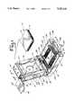
- FIG. 1is a perspective view of the IC connector of this invention with an IC package shown just prior to insertion.
- FIG. 2is a perspective view of the IC connector with the package inserted and the latch in a partially closed position.
- FIG. 3is a perspective view similar to FIG. 2, but showing the latch in a fully closed position.
- FIG. 4is a sectional view of the connector with the latch in a full open position taken along line 4--4 of FIG. 1.
- FIG. 5is a sectional view of the connector with the latch in a partially closed position.
- FIG. 6is a sectional view of the connector with the latch in a fully closed position.
- FIG. 7is a front sectional view taken along line 7--7 of FIG. 6.
- FIG. 8is a sectional view of the connector with the latch in a full open position taken along line 8--8 of FIG. 1.
- FIG. 9is a sectional view of the connector similar to FIG. 8 with the latch in a partially closed position.
- FIG. 10is a sectional view of the connector similar to FIG. 8 with the latch in a fully closed position.
- FIG. 1show the IC chip connector 10 of this invention.
- IC chip connector 10 shown in the drawingswhich for illustrative purposes, is shown as a typical leaded IC chip 2 with a carrier package.
- the connector of this inventionis not limited to any type or configuration of IC chip, whether leaded or leadless.
- the connector of this inventioncan also be used with conventional carrier packages as described in U.S. Pat. No. 4,435,724, incorporated herein by reference.
- Connector 10includes a body 12, which includes side walls 13, 15, and end walls 14, 16. Walls 13, 14, 15, and 16 form a top face 20 about a central opening 18. Alignment posts 24 extend upwardly from top face 20 at each corner of central opening 18. Each alignment post 24 has a vertical recess 25 for accepting the corners of IC chip 2.
- Body 12defines grooves 22 located peripherally of center opening 18 as shown to accommodate leads 6 of chip 2.
- Electrically conductive contacts 30are fitted in grooves 22 and extend below the bottom surface 21 of body 12 for electrical connection to a PC board (not shown). Contacts 30 also extend partially upward through top face 20. Leads 6 and contacts 30 are in electrical contact when IC chip 2 is secured to connector 10 during proper testing conditions.
- IC chip 2and the orientation of grooves 22 will depend on the configuration and number of leads of IC chip 2.
- the configuration and orientation illustrateddoes not limit the invention to those designs but is shown for purpose of description only.
- End wall 14 of connector 10includes a catch plate 26, which defines spaced slots 27, 28. Each slot 27, 28 defines an upper lip 29.
- Opposite end wall 16 of connector 10includes raised tabs 32.
- a rod 34extends through tabs 32 and is secured stationary relative to connector 10.
- Latching mechanism 36 shown in FIGS. 1-3includes latch plate 40, which has ears 42.
- Rod 34extends through ears 42 as shown in FIG. 2 to rotationally secure latch plate 40 to body 12.
- Helical spring 38circumscribes rods 34 and serves to urge latch plate 40 towards the latched position (FIG. 3).
- Latch plate 40has a vent hole 41, which is aligned with connector center opening 18 when latch plate 40 is in a latched position (FIG. 3).
- Latch plate 40also includes raised side walls 43, 44 and top lips 46, 47. As shown in FIG. 4, each lip 46, 47 includes an opposed extension 48, 49, which projects towards the center of latch plate 40 with an end of spring 38 housed in the space between the extension 49 and side wall 43.
- Raised side walls 43, 44also include a centrally positioned through bore 45.
- Latch plate 40also pivotally supports contact pad frame 50.
- Contact frame 50is preferably constructed of a durable metal, such as aluminum.
- Contact frame 50has a generally rectangular configuration with two raised opposite side walls 51, 52. Each raised side wall 51 and 52 has a centrally positioned through bore 53.
- Contact frameis pivotally mounted to latch plate 40 by pivot pins 54 fitted within aligned bores 43 and 53 in latch plate 40 and contact frame 50.
- Contact frame 50pivots relative to latch plate 40 about a lateral axis through contact pins 54.
- Contact frame 50carries a contact pad 56.
- Contact pad 56is constructed of a non-conductive semi-malleable material such as plastic. Contact pad 56 provides a relatively malleable surface for urging IC chip leads 6 against contacts 30 without damaging either the leads or contacts.
- Contact pad 56is secured to contact frame 50 by any conventional method, such as by screws 59.
- Contact frame 50 and pad 56define a central opening 55 for accommodating IC chip body 4 in an overlying relation.
- Contact frame 50 and pad 56also define apertures 57 in each corner to accommodate alignment posts 24 of IC chip body 4.
- a rod 68is connected between and spans latch plate walls 43, 44.
- Actuator plate 60is rotatably connected to rod 68 as shown in FIG. 2.
- Actuator plate 60as best shown in FIG. 2, includes legs 64, which have feet 65.
- Rod 68extends through feet 65.
- Actuator platealso includes oppositely located side flanges 66, 67, which bear against extensions 48, 49 to secure actuator plate 60 and latch plate 40 in the latched position of FIG. 3.
- Actuator plate 60also includes inclined handle part 62 to facilitate use and a vent hole 61, which is aligned with vent hole 41 of latch plate 40.
- Springs 69urge actuator plate 60 toward the unlatched position of FIG. 1.
- Latch hook member 70is rotatably connected to actuator plate 60 through a rod 76 which spans actuator feet 65 and is secured thereto by retainer ring 77 (not shown).
- Hook member 70includes a one-piece upper portion 72, which overlies rod 76 and a depending lower hook portion 74, which includes peripheral hooks 75.
- Spring 78is connected to rod 76 and bears on rod 68 to bias hook member 70 in a latched position.
- FIGS. 4-8illustrate the operation of connector 10 through a series of sectional views.
- FIG. 4illustrates the connector 10 with latching mechanism 36 in a full open position, which allows the IC chip 2 to be placed in the connector such that IC leads 6 overlie and engage contacts 30 as shown. Latching mechanism 36 is then pivoted as shown in FIGS. 4-10 to secure the IC chip 2 for testing.
- connector 10will be secured to a PC board (not shown) before latching mechanism 36 is closed. This will allow one handed operation of the latching mechanism 36.
- a usergrasps actuator handle 62 and pushes or pulls in the direction of arrow 90. This action causes latch plate 40 to pivot about rod 34.
- contact pad 56is positioned to engage leads 6 of IC chip 2.
- the pivoting action of contact frame 50allows for uniform alignment of pads 56 over the IC leads 6 as latch plate 40 is lowered. This allows substantially all of the leads 6 to be pressed at the same time to ensure uniform locking engagement with contacts 30.
- the projection 80 of hook member 70contacts latch plate 40 urging the hooks 75 to position in slots 27, 28 of catch plate 26.
- actuator plate 60is then pivoted about rod 68 to properly position hook part 70.
- the userthen pulls or pushes actuator handle 62 in the direction of arrow 92 (FIG. 5).
- This actionpulls rod 76 and its connected hook part forward, towards rod 34 and over the center axis of the rod 76.
- This over-center pivotingcreates a moment, which is related to the ratio of the distance between the centerline of rod 76 to the end of actuator plate 60 over the diminishing angle.
- the actuatoris secured in a snap-fit manner between side wall 43, 44 by extensions 49, 48 (FIGS. 6, 7 and 10).
- latching mechanism 36To disengage latch mechanism 36, the reverse of the above procedure is followed. With the latch plate 40 in the locked position of FIGS. 6, 7 and 10, the user pulls up on actuator plate handle 62. This causes rod 76 to shift away from rod 34 urging rod 76 over the center axis of rod 68. Projection 80 then rides on latch plate 40 forcing hook part 70 to move away from rod 34. When hook portion 75 disengages from slots 27, 28 the latching mechanism 36 may be pivoted into the open position. The IC package 2 may then be removed from connector 10 and an IC package inserted for IC testing.
Landscapes
- Engineering & Computer Science (AREA)
- Microelectronics & Electronic Packaging (AREA)
- Connecting Device With Holders (AREA)
Abstract
Description
Claims (15)
Priority Applications (1)
| Application Number | Priority Date | Filing Date | Title |
|---|---|---|---|
| US08/019,552US5387120A (en) | 1993-02-19 | 1993-02-19 | Latching IC connector |
Applications Claiming Priority (1)
| Application Number | Priority Date | Filing Date | Title |
|---|---|---|---|
| US08/019,552US5387120A (en) | 1993-02-19 | 1993-02-19 | Latching IC connector |
Publications (1)
| Publication Number | Publication Date |
|---|---|
| US5387120Atrue US5387120A (en) | 1995-02-07 |
Family
ID=21793818
Family Applications (1)
| Application Number | Title | Priority Date | Filing Date |
|---|---|---|---|
| US08/019,552Expired - Fee RelatedUS5387120A (en) | 1993-02-19 | 1993-02-19 | Latching IC connector |
Country Status (1)
| Country | Link |
|---|---|
| US (1) | US5387120A (en) |
Cited By (27)
| Publication number | Priority date | Publication date | Assignee | Title |
|---|---|---|---|---|
| WO1998030465A1 (en)* | 1997-01-07 | 1998-07-16 | Fluoroware, Inc. | Integrated circuit tray with self aligning pocket |
| US5785535A (en)* | 1996-01-17 | 1998-07-28 | International Business Machines Corporation | Computer system with surface mount socket |
| US5924183A (en)* | 1996-12-13 | 1999-07-20 | Cirrus Logic, Inc. | Method of adapting a hand test socket for use in a workpress assembly |
| US6155859A (en)* | 1998-02-27 | 2000-12-05 | Enplas Corporation | IC socket having pressure cover and associated stopper |
| US6297654B1 (en) | 1999-07-14 | 2001-10-02 | Cerprobe Corporation | Test socket and method for testing an IC device in a dead bug orientation |
| US6354859B1 (en)* | 1995-10-04 | 2002-03-12 | Cerprobe Corporation | Cover assembly for an IC socket |
| US6676429B1 (en)* | 2002-12-10 | 2004-01-13 | Hon Hai Precision Ind. Co., Ltd. | Land grid array connector assembly |
| US6692280B2 (en)* | 2001-09-28 | 2004-02-17 | Intel Corporation | Socket warpage reduction apparatus and method |
| US6716050B1 (en)* | 2002-12-20 | 2004-04-06 | Hon Hai Precision Ind. Co., Ltd. | Land grid array connector assembly having a stiffener with pivot bores |
| US20040095693A1 (en)* | 2002-10-31 | 2004-05-20 | Hiroshi Shirai | LGA package socket |
| US20040097119A1 (en)* | 2002-11-15 | 2004-05-20 | Hao-Yun Ma | Land grid array socket with reinforcing plate |
| US20040219808A1 (en)* | 2003-04-30 | 2004-11-04 | Mcclellan Justin Shane | Electronic package with socket and reinforced cover assembly |
| US20050032408A1 (en)* | 2003-08-08 | 2005-02-10 | Fang-Jwu Liao | Electrical connector |
| US20050042897A1 (en)* | 2003-08-22 | 2005-02-24 | Jian Zhang | Electrical connector |
| US20070029811A1 (en)* | 2004-10-21 | 2007-02-08 | Kostuchowski Cory R | Single latch manual actuator for testing microcircuits, and having a mechanical interlock for controlling opening and closing |
| US20070155215A1 (en)* | 2005-12-29 | 2007-07-05 | Hon Hai Precision Ind. Co., Ltd. | Land grid array connector with cover member |
| US20070218742A1 (en)* | 2006-03-17 | 2007-09-20 | Chih-Ming Lai | Chip Adapter Seat |
| US20080207037A1 (en)* | 2007-02-23 | 2008-08-28 | Nasser Barabi | Chip actuator cover assembly |
| US20110039425A1 (en)* | 2009-08-11 | 2011-02-17 | Hon Hai Precision Industry Co., Ltd. | Burn-in socket assembly with base having protruding strips |
| US20160081197A1 (en)* | 2014-09-12 | 2016-03-17 | International Business Machines Corporation | Compute intensive module packaging |
| US20160157359A1 (en)* | 2014-11-07 | 2016-06-02 | International Business Machines Corporation | Customized module lid |
| DE102017003683A1 (en)* | 2017-04-18 | 2018-10-18 | Franka Emika Gmbh | Method for transferring a component to be tested and robot for carrying out this method |
| JP2020148491A (en)* | 2019-03-11 | 2020-09-17 | 株式会社エス・イー・アール | Ic package testing apparatus |
| US11022645B2 (en)* | 2019-11-05 | 2021-06-01 | Prowell | Semiconductor element test device |
| US11128071B2 (en)* | 2019-10-25 | 2021-09-21 | Schweitzer Engineering Laboratories, Inc. | Interface for a printed circuit board assembly adapter module |
| US11531043B2 (en)* | 2018-05-11 | 2022-12-20 | Advantest Corporation | Test carrier and carrier assembling apparatus |
| US20230261398A1 (en)* | 2022-02-16 | 2023-08-17 | Foxconn (Kunshan) Computer Connector Co., Ltd. | Chip connector with an improved rotating plate |
Citations (6)
| Publication number | Priority date | Publication date | Assignee | Title |
|---|---|---|---|---|
| US4758176A (en)* | 1986-07-10 | 1988-07-19 | Yamaichi Electric Mfg. Co., Ltd. | IC socket |
| US5009608A (en)* | 1990-07-12 | 1991-04-23 | Amp Incorporated | Separable connector assembly for an IC Chip Carrier |
| US5044810A (en)* | 1988-08-05 | 1991-09-03 | Yamaichi Electric Mfg. Co., Ltd. | IC socket having cover with locking member |
| US5100332A (en)* | 1989-12-28 | 1992-03-31 | Yamaichi Electric Mfg. Co., Ltd. | IC socket |
| US5120238A (en)* | 1991-03-15 | 1992-06-09 | Wells Electronics, Inc. | Latching IC connector |
| US5176524A (en)* | 1990-10-25 | 1993-01-05 | Canon Kabushiki Kaisha | IC socket structure |
- 1993
- 1993-02-19USUS08/019,552patent/US5387120A/ennot_activeExpired - Fee Related
Patent Citations (6)
| Publication number | Priority date | Publication date | Assignee | Title |
|---|---|---|---|---|
| US4758176A (en)* | 1986-07-10 | 1988-07-19 | Yamaichi Electric Mfg. Co., Ltd. | IC socket |
| US5044810A (en)* | 1988-08-05 | 1991-09-03 | Yamaichi Electric Mfg. Co., Ltd. | IC socket having cover with locking member |
| US5100332A (en)* | 1989-12-28 | 1992-03-31 | Yamaichi Electric Mfg. Co., Ltd. | IC socket |
| US5009608A (en)* | 1990-07-12 | 1991-04-23 | Amp Incorporated | Separable connector assembly for an IC Chip Carrier |
| US5176524A (en)* | 1990-10-25 | 1993-01-05 | Canon Kabushiki Kaisha | IC socket structure |
| US5120238A (en)* | 1991-03-15 | 1992-06-09 | Wells Electronics, Inc. | Latching IC connector |
Cited By (47)
| Publication number | Priority date | Publication date | Assignee | Title |
|---|---|---|---|---|
| US6354859B1 (en)* | 1995-10-04 | 2002-03-12 | Cerprobe Corporation | Cover assembly for an IC socket |
| US5785535A (en)* | 1996-01-17 | 1998-07-28 | International Business Machines Corporation | Computer system with surface mount socket |
| US5924183A (en)* | 1996-12-13 | 1999-07-20 | Cirrus Logic, Inc. | Method of adapting a hand test socket for use in a workpress assembly |
| US6018248A (en)* | 1996-12-13 | 2000-01-25 | Cirrus Logic, Inc. | Frame for holding a bladed element of an IC handling system |
| US6111420A (en)* | 1996-12-13 | 2000-08-29 | Cirrus Logic, Inc. | Fine alignment IC handler and method for assembling the same |
| US5791486A (en)* | 1997-01-07 | 1998-08-11 | Fluoroware, Inc. | Integrated circuit tray with self aligning pocket |
| WO1998030465A1 (en)* | 1997-01-07 | 1998-07-16 | Fluoroware, Inc. | Integrated circuit tray with self aligning pocket |
| US6155859A (en)* | 1998-02-27 | 2000-12-05 | Enplas Corporation | IC socket having pressure cover and associated stopper |
| US6297654B1 (en) | 1999-07-14 | 2001-10-02 | Cerprobe Corporation | Test socket and method for testing an IC device in a dead bug orientation |
| US20080119081A1 (en)* | 2001-09-28 | 2008-05-22 | Intel Corporation | Socket warpage reduction apparatus |
| US6692280B2 (en)* | 2001-09-28 | 2004-02-17 | Intel Corporation | Socket warpage reduction apparatus and method |
| US20040147156A1 (en)* | 2001-09-28 | 2004-07-29 | Intel Corporation. | Socket warpage reduction apparatus and method |
| US7350299B2 (en) | 2001-09-28 | 2008-04-01 | Intel Corporation | Method for reducing socket warpage |
| US20040095693A1 (en)* | 2002-10-31 | 2004-05-20 | Hiroshi Shirai | LGA package socket |
| US7001197B2 (en)* | 2002-10-31 | 2006-02-21 | Tyco Electronics Amp K.K. | Land grid array socket |
| US20040097119A1 (en)* | 2002-11-15 | 2004-05-20 | Hao-Yun Ma | Land grid array socket with reinforcing plate |
| US6848929B2 (en)* | 2002-11-15 | 2005-02-01 | Hon Hai Precision Ind. Co., Ltd. | Land grid array socket with reinforcing plate |
| US6676429B1 (en)* | 2002-12-10 | 2004-01-13 | Hon Hai Precision Ind. Co., Ltd. | Land grid array connector assembly |
| US6716050B1 (en)* | 2002-12-20 | 2004-04-06 | Hon Hai Precision Ind. Co., Ltd. | Land grid array connector assembly having a stiffener with pivot bores |
| US20040219808A1 (en)* | 2003-04-30 | 2004-11-04 | Mcclellan Justin Shane | Electronic package with socket and reinforced cover assembly |
| US6945798B2 (en)* | 2003-04-30 | 2005-09-20 | Tyco Electronics Corporation | Electronic package with socket and reinforced cover assembly |
| US20050032408A1 (en)* | 2003-08-08 | 2005-02-10 | Fang-Jwu Liao | Electrical connector |
| US6932622B2 (en)* | 2003-08-08 | 2005-08-23 | Hon Hai Precision Ind. Co., Ltd. | Electrical connector |
| US20050042897A1 (en)* | 2003-08-22 | 2005-02-24 | Jian Zhang | Electrical connector |
| US20070029811A1 (en)* | 2004-10-21 | 2007-02-08 | Kostuchowski Cory R | Single latch manual actuator for testing microcircuits, and having a mechanical interlock for controlling opening and closing |
| US7567075B2 (en)* | 2004-10-21 | 2009-07-28 | Kostuchowski Cory R | Single latch manual actuator for testing microcircuits, and having a mechanical interlock for controlling opening and closing |
| US20070155215A1 (en)* | 2005-12-29 | 2007-07-05 | Hon Hai Precision Ind. Co., Ltd. | Land grid array connector with cover member |
| US7387523B2 (en)* | 2005-12-29 | 2008-06-17 | Hon Hai Precision Ind. Co., Ltd | Land grid array connector with cover member |
| US20070218742A1 (en)* | 2006-03-17 | 2007-09-20 | Chih-Ming Lai | Chip Adapter Seat |
| US7297011B2 (en)* | 2006-03-17 | 2007-11-20 | Giga-Gyte Technology Co. Ltd. | Chip adapter seat |
| US20080207037A1 (en)* | 2007-02-23 | 2008-08-28 | Nasser Barabi | Chip actuator cover assembly |
| US7651340B2 (en) | 2007-02-23 | 2010-01-26 | Essai, Inc. | Chip actuator cover assembly |
| US20110039425A1 (en)* | 2009-08-11 | 2011-02-17 | Hon Hai Precision Industry Co., Ltd. | Burn-in socket assembly with base having protruding strips |
| US8057242B2 (en)* | 2009-08-11 | 2011-11-15 | Hon Hai Precision Ind. Co., Ltd. | Burn-in socket assembly with base having protruding strips |
| US9818667B2 (en)* | 2014-09-12 | 2017-11-14 | International Business Machines Corporation | Compute intensive module packaging |
| US20160081197A1 (en)* | 2014-09-12 | 2016-03-17 | International Business Machines Corporation | Compute intensive module packaging |
| US20160157359A1 (en)* | 2014-11-07 | 2016-06-02 | International Business Machines Corporation | Customized module lid |
| US10163742B2 (en)* | 2014-11-07 | 2018-12-25 | International Business Machines Corporation | Customized module lid |
| US11270919B2 (en) | 2014-11-07 | 2022-03-08 | International Business Machines Corporation | Customized module lid |
| DE102017003683A1 (en)* | 2017-04-18 | 2018-10-18 | Franka Emika Gmbh | Method for transferring a component to be tested and robot for carrying out this method |
| US11531043B2 (en)* | 2018-05-11 | 2022-12-20 | Advantest Corporation | Test carrier and carrier assembling apparatus |
| JP2020148491A (en)* | 2019-03-11 | 2020-09-17 | 株式会社エス・イー・アール | Ic package testing apparatus |
| US11128071B2 (en)* | 2019-10-25 | 2021-09-21 | Schweitzer Engineering Laboratories, Inc. | Interface for a printed circuit board assembly adapter module |
| US20210376506A1 (en)* | 2019-10-25 | 2021-12-02 | Schweitzer Engineering Laboratories, Inc. | Interface for a printed circuit board assembly adapter module |
| US11626675B2 (en)* | 2019-10-25 | 2023-04-11 | Schweitzer Engineering Laboratories, Inc. | Interface for a printed circuit board assembly adapter module |
| US11022645B2 (en)* | 2019-11-05 | 2021-06-01 | Prowell | Semiconductor element test device |
| US20230261398A1 (en)* | 2022-02-16 | 2023-08-17 | Foxconn (Kunshan) Computer Connector Co., Ltd. | Chip connector with an improved rotating plate |
Similar Documents
| Publication | Publication Date | Title |
|---|---|---|
| US5387120A (en) | Latching IC connector | |
| TW437037B (en) | Vertically actuated bag socket | |
| US5120238A (en) | Latching IC connector | |
| US20050208813A1 (en) | Electrical connector socket with loading caddy | |
| US4789345A (en) | Socket device for fine pitch lead and leadless integrated circuit package | |
| KR200165887Y1 (en) | Socket for inspection of ball grid array package | |
| US6547580B1 (en) | Socket apparatus particularly adapted for land grid array type semiconductor devices | |
| US5044810A (en) | IC socket having cover with locking member | |
| JPH07240263A (en) | Burn-in receptacle | |
| US5312267A (en) | Socket for the use of electric part | |
| US5290192A (en) | Chip carrier socket | |
| US5009608A (en) | Separable connector assembly for an IC Chip Carrier | |
| US20010053628A1 (en) | Socket for electrical parts | |
| JP2854276B2 (en) | Tray unit for semiconductor device test | |
| US4560217A (en) | Chip carrier connector | |
| US5000696A (en) | Lock mechanism in an IC socket | |
| US4669796A (en) | RAM connector | |
| US6570398B2 (en) | Socket apparatus particularly adapted for LGA type semiconductor devices | |
| US6863553B2 (en) | Socket for electrical parts | |
| US5409392A (en) | Burn-in socket | |
| JPH10106706A (en) | Test socket for integrated circuit | |
| US5352131A (en) | IC socket | |
| JP2004079227A (en) | IC socket | |
| US7059885B2 (en) | Land grid array connector with horizontal stop | |
| US5205756A (en) | Chip carrier socket |
Legal Events
| Date | Code | Title | Description |
|---|---|---|---|
| AS | Assignment | Owner name:WELLS ELECTRONICS, INC., INDIANA Free format text:ASSIGNMENT OF ASSIGNORS INTEREST.;ASSIGNORS:MARKS, RICHARD L.;MILBRAND, DONALD W., JR.;REEL/FRAME:006469/0889 Effective date:19930222 | |
| AS | Assignment | Owner name:FLEET NATIONAL BANK, MASSACHUSETTS Free format text:ASSIGNMENT OF ASSIGNORS INTEREST;ASSIGNOR:WELLS ELECTRONICS, INC.;REEL/FRAME:009350/0588 Effective date:19971226 | |
| FPAY | Fee payment | Year of fee payment:4 | |
| AS | Assignment | Owner name:WELLS-CTI, INC., INDIANA Free format text:MERGER AND CHANGE OF NAME;ASSIGNOR:WELLS ELECTRONICS, INC.;REEL/FRAME:009375/0722 Effective date:19980731 | |
| FEPP | Fee payment procedure | Free format text:PAYOR NUMBER ASSIGNED (ORIGINAL EVENT CODE: ASPN); ENTITY STATUS OF PATENT OWNER: LARGE ENTITY Free format text:PAYER NUMBER DE-ASSIGNED (ORIGINAL EVENT CODE: RMPN); ENTITY STATUS OF PATENT OWNER: LARGE ENTITY | |
| AS | Assignment | Owner name:FLEET NATIONAL BANK, AS AGENT, MASSACHUSETTS Free format text:SECURITY AGREEMENT;ASSIGNOR:WELLS-CTI INC.;REEL/FRAME:012795/0323 Effective date:20020227 | |
| FPAY | Fee payment | Year of fee payment:8 | |
| REMI | Maintenance fee reminder mailed | ||
| AS | Assignment | Owner name:KABUSHIKI WELLS-CTI, LLC., OREGON Free format text:ASSIGNMENT OF ASSIGNORS INTEREST;ASSIGNOR:WELLS-CTI, INC.;REEL/FRAME:013746/0292 Effective date:20030503 | |
| AS | Assignment | Owner name:WELLS-CTI, LLC., AN OREGON LIMITED LIABILITY COMPA Free format text:ASSIGNMENT OF ASSIGNORS INTEREST;ASSIGNOR:KABUSHIKI WELLS-CTI, LLC, AN OREGON LIMITED LIABILITY COMPANY;REEL/FRAME:013868/0042 Effective date:20030617 | |
| AS | Assignment | Owner name:SILICON VALLEY BANK, CALIFORNIA Free format text:SECURITY AGREEMENT;ASSIGNOR:WELLS-CTI LLC;REEL/FRAME:014646/0735 Effective date:20030813 | |
| FEPP | Fee payment procedure | Free format text:PAYER NUMBER DE-ASSIGNED (ORIGINAL EVENT CODE: RMPN); ENTITY STATUS OF PATENT OWNER: LARGE ENTITY Free format text:PAYOR NUMBER ASSIGNED (ORIGINAL EVENT CODE: ASPN); ENTITY STATUS OF PATENT OWNER: LARGE ENTITY | |
| REMI | Maintenance fee reminder mailed | ||
| LAPS | Lapse for failure to pay maintenance fees | ||
| STCH | Information on status: patent discontinuation | Free format text:PATENT EXPIRED DUE TO NONPAYMENT OF MAINTENANCE FEES UNDER 37 CFR 1.362 | |
| FP | Lapsed due to failure to pay maintenance fee | Effective date:20070207 | |
| AS | Assignment | Owner name:WELLS-CTI LLC, WASHINGTON Free format text:RELEASE;ASSIGNOR:SILICON VALLEY BANK;REEL/FRAME:029430/0791 Effective date:20121127 |