US5386518A - Reconfigurable computer interface and method - Google Patents
Reconfigurable computer interface and methodDownload PDFInfo
- Publication number
- US5386518A US5386518AUS08/017,222US1722293AUS5386518AUS 5386518 AUS5386518 AUS 5386518AUS 1722293 AUS1722293 AUS 1722293AUS 5386518 AUS5386518 AUS 5386518A
- Authority
- US
- United States
- Prior art keywords
- data
- control signals
- state
- state machine
- reconfigurable
- Prior art date
- Legal status (The legal status is an assumption and is not a legal conclusion. Google has not performed a legal analysis and makes no representation as to the accuracy of the status listed.)
- Expired - Lifetime
Links
Images


Classifications
- G—PHYSICS
- G06—COMPUTING OR CALCULATING; COUNTING
- G06F—ELECTRIC DIGITAL DATA PROCESSING
- G06F13/00—Interconnection of, or transfer of information or other signals between, memories, input/output devices or central processing units
- G06F13/38—Information transfer, e.g. on bus
- G06F13/382—Information transfer, e.g. on bus using universal interface adapter
- G06F13/385—Information transfer, e.g. on bus using universal interface adapter for adaptation of a particular data processing system to different peripheral devices
Definitions
- the present inventionrelates to computer interface control circuitry. More specifically, the present invention relates to methods and apparatus for providing a high speed, programmable interface circuit for use with computers or other data or signal processing equipment.
- Computer interface control circuitsare utilized to connect an external peripheral device such as a tape drive, disk drive, sensor device or the like to the internal circuitry of signal or data processing equipment.
- External peripheral devicesoften communicate with the signal and data processing equipment in accordance with different protocols (e.g., data formats, signal levels, framing of words, timing of bits, etc.).
- signal and data processing equipmentoften support multiple external devices. Therefore, a computer interface control circuit often must be reconfigured for each external device that it is connected to. The interface often also utilizes a different protocol from that used by the interfaced circuits.
- a hardwired logic interfaceis a special purpose, dedicated interface circuit that typically exhibits a fast data rate.
- a major disadvantage of the hardwired logic interfaceis that it is not reconfigurable.
- the hardwired logic interfaceenables communication between the processing equipment and a particular external device. However, it cannot be easily modified to permit communication between the processing equipment and another external peripheral device without time consuming physical circuit changes.
- the hardwired logic interfacerequires a different hardware logic design for each change to the interface protocol.
- the PROM based state machine interfaceis also designed to operate with a particular external peripheral device.
- the PROM based interfacehas the disadvantage of requiring that the PROM be reprogrammed or replaced in order to reconfigure the interface to support a different external device. This requirement results in substantial downtime of the external device and hardware changes to the interface. Therefore, when utilizing the PROM based interface, a separate PROM based circuit is required for each external device that the interface supports.
- the microprocessor controlled interfaceis easily reconfigurable while in the circuit between the signal processing equipment and the external device. However, a dedicated microprocessor is required. Although the dedicated microprocessor is typically fast, the execution of multiple instructions for each interface control activity results in a slow interface relative to the system clock speed. Therefore, the microprocessor controlled interface does not support high data rates.
- a computer interface control circuitis not available that is easily reconfigurable while in circuit for connecting a plurality of external devices to the signal or data processing equipment that can adapt to a variety of interface protocols, is autonomous of a host computer and provides a high rate of data transfer.
- the need in the artis addressed by the reconfigurable computer interface and method of the present invention.
- the inventionis employed for interfacing a first subsystem to a second subsystem and includes a reconfigurable state machine for generating a plurality of interface control signals in accordance with a state table in response to a plurality of mode control signals.
- a first mechanismis included for generating the state table and a second mechanism is provided for generating the mode control signals for the reconfigurable state machine.
- an initiation logic devicegenerates and downloads a state table and a plurality of mode control signals to a programmable state machine when the reconfigurable computer interface is utilized to connect a new external peripheral device to a signal processing system.
- the state tabledefines the characteristics of the state machine and the state machine controls the operation of the reconfigurable computer interface.
- the programmable state machineutilizes the present state, the state table and the mode control signals to determine the next machine state which provides rapid and convenient reconfigurability of the interface circuit to connect a variety of external devices to the signal processing system.
- a bus sizing register circuitis included to modify the word size of a plurality of data signals and temporary memory is also included.
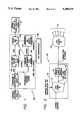
- FIG. 1is a block diagram of an illustrative embodiment of the reconfigurable computer interface of the present invention shown as a communication link between the internal circuitry of a signal processing system and an external peripheral device.
- FIG. 2is a simplified block diagram of a download programmable state machine employed within the reconfigurable computer interface of FIG. 1.
- FIG. 3is a more detailed block diagram of the reconfigurable computer interface of FIG. 1 showing the download programmable state machine as the main structural element of the interface.
- FIG. 4is a circuit diagram of a plurality of bidirectional registers which form the bus sizing register circuit of the reconfigurable computer interface shown in FIGS. 1 and 3.
- FIG. 5is a flow diagram of the method for utilizing the reconfigurable computer interface to connect the internal circuitry of the signal processing system with the external peripheral device.
- the inventionis a reconfigurable computer interface 100 as shown in FIG. 1.
- the interface 100is positioned between the internal circuitry of a signal processing system 102 and at least one external peripheral device 104 and serves as a communication link therebetween.
- the signal processing system 102can be any suitable fixed hardware signal or data processing equipment ranging from a portion of a circuit card to a mainframe computer.
- the external device 104can be any of a wide variety of computer peripheral equipment such as, for example, a tape drive, a disk drive, an infrared or temperature or electromagnetic sensor, digital or video equipment and the like.
- the interface 100is also connected to a host microprocessor 106 for receiving a plurality of control data therefrom.
- the host microprocessor 106can be any processing device suitable for providing the plurality of control data to the interface 100 as discussed hereinbelow.
- the host 106includes software written in a high level language in the form of a state equation. When the software is compiled and executed in the host 106, the plurality of control data (e.g., a block of state table data) is generated.
- the block of state table dataincludes both a state table and a plurality of control signals or mode signals which fully define the operating characteristics of the interface 100. The accuracy of the state table data can be verified prior to utilization by executing the software program on a computer and saving the state table data to file for subsequent analysis.
- the state table datais generated and downloaded to the interface 100 within a few milliseconds. It is noted that the operation of the interface 100 is completely autonomous of the host 106 after the state table and plurality of mode signals have been downloaded.
- the interface 100includes a download programmable state machine 108 as shown in FIG. 1.
- the state machine 108receives and is initialized by the block of state table data downloaded from the host 106.
- the state table generated by and downloaded from the host 106defines the behavior of the state machine 108.
- the mode signalsdetermine which portion of the state table is utilized by the state machine 108 at any instant of time.
- each of the remaining components of the interface 100is controlled by the state machine 108.
- the state machine 108is autonomous from the host 106.
- the efficiency of the host 106is improved since microprocessor time is economized.
- the host 106 and the interface 100can be constructed on the same circuit board. This design eliminates the need for storage space for the block of state table data thus improving the space economy of the present invention.
- the state machine 108which can be implemented in hardware and software, is comprised of a storage element register 110 which is a one-word memory element.
- the register 110stores a logical word containing a specified bit pattern and the logical word defines a particular state of the state machine 108. Thus, at any instant of time, the register 110 stores the present state of the state machine 108.
- the output signal of the register 110is the bit pattern which represents the present state signal.
- the first logic element 112receives several input signals including the present state signal feedback from register 110 on a line 114.
- First logic element 112also receives the downloaded state table data from the host 106 including the state table and the mode signals.
- the mode signalsare part of the external conditions which are applied to the state machine 108 to influence the operation thereof.
- the external conditionsalso include a programmable handshake control from the circuit 150 described hereinbelow.
- the first logic element 112determines what the next state of the state machine 108 should be. The next state signal is then transmitted and stored in the storage element register 110.
- the register 110is also connected to a second logic element 116 as shown in FIG. 2.
- the second logic element 116also receives the present state signal from the register 110 and then generates a plurality of output signals represented by the numeral 118.
- the output signals 118typically are utilized to control other components of the interface 100.
- the generation of the next state signalis influenced by the state table and mode signals received at the first logic element 112 from the host 106.
- the state tableis altered when the interface 100 connects the internal circuitry of the signal processing system 102 to a new external peripheral device 104 different from previous external devices.
- the altered state table and mode signalsrapidly reconfigure the programmable state machine 108 to function as an effective communication link between the processing system 102 and the external device 104. Rapid reconfiguration in the present invention is interpreted to mean that the interface characteristics of the interface 100 can be modified in a matter of minutes verses several months as was required in the prior art. Since the interface 100 is software reconfigurable, it enables a wide variety of external devices 104 having different data formats, signal levels, framing of words, timing of bits, etc. to be connected to the processing system 102 without the need to modify interface hardware.
- the state machine 108is shown in more detail in the specific implementation of the interface 100 illustrated in FIG. 3.
- the state machine 108comprises two main elements including a downloadable random access memory (RAM) 120 and a programmable array logic (PAL) element 122.
- the downloadable RAM 120contains the storage element register 110 which serves to store the current state signal of the state machine 108.
- the downloadable RAM 120also contains a large memory for storing the state table received from the host 106.
- the downloadable RAM 120emulates the function of the first logic element 112 and the storage element register 110 of FIG. 2.
- the first logic element 112is an implementation of the state table.
- the downloadable RAM 120evaluates the present state signal, the state table and the external mode signals to generate the next state signal and the next state output signals.
- the next state signalis stored in the storage element register 110.
- the downloadable RAM 120 of the state machine 108receives the state table and mode signals downloaded from the host 106.
- the mode signals downloaded to the RAM 120 shown in FIG. 3determine which portion of the state table is utilized by the state machine 108. (The mode signals are also shown as external conditions arrowed to the first logic element 112 in FIG. 2.) This design enables several different selectable modes of operation of the state table.
- the host 106generates the mode signals and writes them into a command register 128 as shown in FIG. 3.
- the command register 128provides storage for the mode signals and transfers the mode signals to the programmable state machine 108 on a continuous basis.
- the programmable array logic (PAL) circuit 122 included within the programmable state machine 108emulates the function of the second logic element 116 of FIG. 2.
- the PAL circuit 122decodes part of the current state signals or output signals 118 (shown in FIG. 2) into control signals 124 for a bus sizing register circuit 126 shown in FIG. 3.
- the control signals 124control the loading and enabling of data within the bus sizing register circuit 126.
- the bus sizing register circuit 126is comprised of a plurality of registers 132 shown in FIG. 4.
- the registers 132are connected in a manner to match the word size utilized by the external peripheral device 104 to the word size utilized by the internal circuitry of the signal processing system 102. In effect, this enables the external device 104 to communicate with the processing system 102 and further efficiently utilizes the storage space of a buffer RAM 130 shown in FIG. 1.
- the datais packed. If the input data words from the external device 104 are, for example, eight bits wide and the data words of the signal processing system are, for example, thirty-two bits wide, the data is packed as follows. Four 8-bit words can be packed into a single 32-bit word by the bus sizing registers 132. Conversely, in the output case, data transmitted from the signal processing system 102 to the external peripheral device 104 via the buffer RAM 130 is unpacked. Thus, the larger 32-bit word is reduced in size to, for example, four 8-bit words.
- the state machine controlled bus sizing registers 132enable the internal circuitry of the signal processing system 102 to accept 8, 16 or 32-bit bidirectional or unidirectional data, dependent upon the interface mode selected and the state table that is downloaded to the programmable state machine 108.
- bus sizing registers 132There are eight bus sizing registers 132 shown in FIG. 4, however other combinations may be suitable.
- the bus sizing register elementsactually perform the packing and unpacking of the data words transmitted between the processing system 102 and the external device 104.
- Each bus sizing register 132includes two register elements 136 and two tri-state output buffers 138. As is known in the art, one register element 136 and one buffer 138 are utilized for input data transfers from the external device 104 to the processing system 102. Likewise, the remaining register element 136 and buffer 138 are utilized for output data transfers from the processing system 102 to the external device 104.
- the bus sizing registers 132 of FIG. 4are located within the bus sizing register circuit 126 shown in FIG. 3.
- the data output from each of the registers 132is connected to a differential driver/receiver 140 as shown in FIG. 4. Under the proper conditions, the driver/receivers 140 permit data to pass in both directions.
- the output terminals of the driver/receivers 140are connected to a plurality of data lines identified by the numeral sequence 134A, 134B, 134C and 134D in FIG. 4.
- the data output line from the bus sizing register circuit 126(which combines the plurality of data lines 134A, 134B, 134C and 134D) to an external connector (not shown) is identified by the numeral 134 on FIG. 3.
- the remaining line shown connected between the bus sizing registers 132 and a data memory (e.g., buffer RAM) 130is identified by the numeral 142 on both FIGS. 3 and 4.
- the buffer RAM 130 shown in FIG. 1is located within the data path between the external peripheral device 104 and the signal processing system 102. Under the direction of control signals from the state machine 108, the buffer RAM 130 temporarily stores data transmitted from the external device 104 to the processing system 102. Likewise, the buffer RAM 130 provides temporary storage for data transmitted from the internal circuitry of the processing system 102 to the external device 104. In the specific implementation shown in FIG. 3, the buffer RAM 130 is shown as a (32K ⁇ 32) bit data memory.
- storage addresses located within the buffer RAM 130are allocated by an arbitration and address generator 144 as shown in FIG. 1.
- the buffer RAM 130is accessed.
- the state machine 108sends a memory request to the arbitration and address generator 144 to select a storage location.
- the selected storage locationwhich is selected sequentially, is then transferred to the buffer RAM 130 from the arbitration and address generator 144.
- the buffer RAM 130then stores the data word at the address selected by the arbitration and address generator 144.
- the operation of the arbitration and address generator 144is defined by starting address and ending address parameters. These parameters are loaded into the arbitration and address generator 144 from the host 106 as shown in FIG. 1 prior to beginning the transfer of a block of data.
- the storage location for the data word within the buffer RAM 130is a specific location. As each memory request is received by the arbitration and address generator 144, a specific address is assigned in the buffer RAM 130. Each memory request serves to increment the arbitration and address generator 144 by one count.
- the arbitration and address generator 144is implemented in the form of a memory arbitration device 146 and a memory control address generator (MCAG) 148.
- the memory arbitration device 146inspects the memory requests for data word storage in the data memory (buffer RAM) 130 from the state machine 108 (for data words from the external device 104) and from the internal circuitry (for data words from the processing system 102). After inspection, the memory arbitration device 146 decides which data words are to be entered into the data memory 130 based upon defined access priorities. Thereafter, the memory arbitration device 146 controls access of specific data to the data memory 130 and transmits a memory grant signal to the state machine 108 to indicate admission. The memory grant signal causes the arbitration and address generator 144 to increase the count from the starting address to the ending address by one increment. Additionally, the transmitted memory arbitration grant signal to the state machine 108 indicates that a memory location in the data memory 130 is available.
- the memory control address generator 148serves to generate addresses for the data memory 130.
- the starting address and ending address parameters received from the host 106are loaded into the address generator 148.
- the first address within the data memory 130 assigned by the address generator 148represents the starting address parameter.
- the address generator 148is incremented by one numerical count. When the numerical count reaches the ending address parameter, a transfer complete signal is sent from the address generator 148 to the state machine 108.
- the differential receiver/driver circuit 150 shown in FIG. 1receives and transmits data words between the external peripheral device 104 and the signal processing system 102. Further, the receiver/driver circuit 150 receives control signals from and transfers control signals to the programmable state machine 108. The direction of transmission of the data and control signals is controlled by the state machine 108. In the data path, data words are transmitted to and received from the bus sizing register circuit 126. External peripheral devices 104 often communicate with the signal processing system 102 in different protocols (e.g., data formats, signal levels, framing of words, timing of bits, etc.). Therefore, the receiver/driver circuit 150 functions to translate the electrical level of the control signals and data words received from and sent to the external device 104 to the electrical level of the interface 100.
- protocolse.g., data formats, signal levels, framing of words, timing of bits, etc.
- the differential receiver/driver circuit 150includes a plurality of differential drivers 152 and a plurality of differential receivers 154 shown in FIG. 3, and a plurality of differential driver/receivers 156, 134A, 134B, 134C and 134D as shown in FIGS. 3 and 4, respectively.
- Each of the drivers 152, receivers 154 and receiver/drivers 156 (shown in FIG. 3) and receiver/drivers 134A, 134B, 134C and 134D (shown in FIG. 4)include a plurality of terminations 158 and 159, respectively, that carry control signals and data words to and/or from the external peripheral device 104.
- the input stage of the differential receiver/driver circuit 150includes a large common mode operating range to ensure translation of the control signals and data words that are outside of the normal operating range of the interface 100.
- Each of the control signals input from the receivers 154 and the receiver/drivers 156are connected to an input register circuit 160 to reduce metastable conditions on the control inputs.
- the two control inputs from the receiver/drivers 156are multiplexed with the output signals from the state machine 108 in a multiplexer processing circuit 161. This design enables the state machine 108 to select the external conditions.
- the interface 100has been implemented in a programmable signal processor as part of the input/output control interface (CIO) circuit card assembly (not shown) for connecting an external device 104 to a processing system 102.
- the present inventionperforms as a smart interface utilizing a state table generation program which can comply with specific requirements.
- the interface 100is generally applicable to and finds utility in any data processing, signal processing or computer device 102 that requires an interface which can be quickly reconfigured while in circuit to communicate with a wide variety of external peripheral devices 104.
- the interface 100also enjoys high speed, autonomous operation, supporting data interface rates that are equal to the system clock rate.
- TTLTransistor-Transistor Logic
- ETLEmitter-Coupled Logic
- the interface 100is an input/output port of 32 bits of differential data which is under the control of one or two programmable handshake state machines 108 and 162.
- the data portis configured by the host microprocessor 106 as byte, word or longword bidirectional or as byte or word unidirectional.
- All datais packed to longwords prior to memory storage and unpacked as necessary by the bus sizing register circuit 126 when output. All handshaking and data packing and unpacking is under the control of the programmable state machine 108 or 162.
- Each state machine 108 and 162is implemented with a registered static downloadable RAM 120 that is (4K ⁇ 16) bit with the serial protocol channel.
- the RAM 120has sixteen registered outputs which provide four bits of present state, four bits of pack/unpack register command, six I/O handshake lines, port direction control, memory access request and the transfer complete interrupt.
- the twelve address inputs to the RAM 120receive four bits of the present state feedback, two bits of the microprocessor mode control bits, four I/O handshake lines, memory access granted from memory arbitration 146 and the address generator done interrupt from the memory control & address generator 148.
- the downloadable RAM 120can be loaded with specific state table data from the host 106.
- Data enters and exits the external data lines 134 of the bus sizing register circuit 126(see FIG. 3) which includes the eight bidirectional bus sizing registers 132 (see FIG. 4).
- the control signals for the bus sizing registers 132are decoded from the state machine pack/unpack command and three EMODE bits from the command register 128 shown in FIG. 3. The decoding is completed within the programmable array logic (PAL) circuit 122.
- the data lines 142 of the bus sizing register circuit 126is connected to the data memory 130 which is 32-bits wide and 32K words deep. All accesses to the data memory 130 are 32-bits wide.
- the addressingis from the address generator 148 where one of three address generators or the microprocessor address bus is multiplexed through to the data memory 130.
- the first and second address generators 148are associated with the programmable state machines 108 and 162, respectively.
- the control of the multiplexer processing circuit 161is the result of the state machine 108.
- the memory arbitration device 146accepts memory requests from state machines 108 and 162, an internal global memory port control logic, and the host 106 and determines which device receives the memory grant signal for each memory access time.
- the port handshake lines for state machine 108include two dedicated inputs, two dedicated outputs and two bidirectional handshake lines.
- the maximum port control signals availableare four dedicated inputs, four dedicated outputs and four bidirectional signals. Half of these control signals are associated with state machine 162 and are normally used only in the word or byte unidirectional output mode. Mode control signals are provided by the host 106 via the command register 128.
- some of the registered outputs of the downloadable RAM 120provide the present state of the state machine 108 and others provide bus sizing register command words, I/O handshake lines, memory requests, port direction control and the transfer complete interrupt.
- the present stateis wrapped back to the address input of the downloadable RAM 120 along with external I/O handshake inputs and microprocessor mode inputs to provide stimulus for the next state.
- the state wordis four bits wide which limits the state machine to sixteen possible states.
- the bus sizing registers 132provide the capability of accepting or sending data as bytes, words or longwords in the bidirectional mode and as words or bytes in the unidirectional mode.
- the registersare controlled by the control signals decoded from the bus sizing command bits output from the state machine 108 and the external mode bits from the command register 128.
- In the bidirectional modeonly one downloadable RAM 120 is utilized for control of the port and external jumpers are required for byte and word transfers.
- the bus sizing registers 132then pack two words into one longword prior to transfer to the data memory 130.
- both downloadable RAM'sare used (unidirectional mode)
- two ports of byte or word sizecan be controlled individually by the two state machines 108 and 162. One port is dedicated to the input data and one port is dedicated to the output data.
- bidirectional bus sizing registers 132e.g., U105, U101, U96 and U90.
- the datais clocked into the registers 132 as a 32-bit word and the output is enabled.
- the differential drivers 140are enabled together for a longword, two at a time for a word transfer and one at a time for a byte transfer under control of the state machine 108.
- the output signalsare enabled when the IEx signals are active low.
- All of the input differential receivers 154are enabled. The inputs are enabled when the IEx signals are active high. Longword inputs are enabled when the clock enable controls for all four bidirectional registers are asserted at once under control of the state machine 108. Word transfers are input by enabling bus sizing registers 132 (e.g., U90 and U96) first and then bus sizing registers 132 (e.g., U101 and U105) second. Byte transfers are input by enabling the registers 132 one at a time. The B outputs of all four registers 132 are then turned on together to enable a longword write to the data memory 130.
- bus sizing registers 132e.g., U90 and U96
- bus sizing registers 132e.g., U101 and U105
- unidirectional transfersare only possible for word and byte size data.
- Unidirectional input transfersare controlled by state machine 108.
- Differential receivers 140e.g., U18, U17, U16 and U15
- Differential receivers 140are enabled to select bits 00 through 15 as the input data.
- the port A clock enablesare asserted for registers 132 (e.g., U95 and U89) first then port A clock enables registers 132 (e.g., U105 and U101) second.
- the port B outputenables for the same four registers 132 to provide a single longword write to the data memory 130.
- the unidirectional output transfersare controlled by state machine 162.
- Differential drivers 140e.g., U14, U13, U12 and U11
- registers 132e.g., U96, U90, U104 and U100
- the differential drivers 140 for bits 16 through 31e.g., U24, U23, U22 and U21 are enabled.
- the port A output enableis also asserted for registers 132 (e.g., U96 and U90) to output the first word and then followed by the port A output enable for registers 132 (e.g., U104 and U100) to output the second word.
- registers 132e.g., U96 and U90
- the port A output enable for registers 132e.g., U104 and U100
- Byte size unidirectional transfersare performed in a similar manner as the word transfers with the exception that only two of the differential drivers 140 are enabled at any one time (8 bits) and the transfer is two cycles longer.
- the byte transferrequires that bits 16 through 23 be jumped to bits 24 through 31 at the cabinet connector.
- the memory control and address generator 148is the address generator for the three port controllers and the buffer for addresses from the local bus (host 106). This is the sole source of addressing to the buffer RAM 130.
- the three port controllersare the two interface ports and the internal global memory port.
- the memory control and address generator 148includes three 15-bit address generators, ending address latches, and comparators (not shown). It also includes a four-to-one multiplexer and a readback capability for the selected address generator output.
- the memory control and address generator 148is set up via a 15 bit data bus and a 15 bit address bus from the host 106 and is controlled by memory grant signals from the data memory arbitration logic 146. Each address generator receives a starting address and an ending address for the transfer to or from the data memory 130. Each address generator output can be read-back as a test and status feature.
- An example download programis representative of the software used to generate data for download to the programmable state machine 108 and software necessary to implement the same.
- the state machine 108is programmed to control a 32-bit bidirectional transfer to and from another circuit card.
- the software program listingis included in Appendix "A" on pages A1 to A4 located at the end of the instant specification.
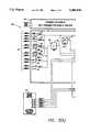
- the associated state diagram shown in FIG. 5is a graphical representation of the case statements used in the computer program entitled SPC #1 Download Data For IO Test With DIO And CIO.
- the state diagramstarts in the IDLE mode and waits for an input to select a branch to the right or a branch to the left.
- the branch to the leftrepresents a transition to a data input mode.
- the branch to the rightrepresents a transition to a data output mode. Once the branch has been taken, the path must be followed until reaching the DONE state.
- the followingis a description of the individual states.
- the state machine 108will automatically transition to the IDLE -- L state at the beginning of the next clock cycle (time increment).
- the reconfigurable computer interface 100outputs the sensor clock (SCLK) to a HIGH level and holds the ready signal (CRDY) to an inactive HIGH level.
- the first pathis back to IDLE -- H and this path is selected if the microprocessor command word is still set to zero. As long as the command word is set to zero, the states will cycle between IDLE -- H and IDLE -- L. The purpose for this cycle is to provide a sensor clock to the external device 104.
- the second pathis to the OUT -- GO state.
- the HIGH INTAG -- L signalis an indication that the address generator has been initialized for the impending transfer of data. This signal stays high until the required number of data words have been transferred.
- the third pathis to the CIO -- IN state.
- the HIGH INTAG -- L signalis an indication that the address generator has been initialized for the impending transfer of data. The signal stays high until the required number of data words have been transferred.
- the interface 100outputs the sensor clock (SCLK) to a LOW level and holds the ready signal (CRDY) to an inactive HIGH level.
- SCLKsensor clock
- CRDYready signal
- the first possible pathis from the IDLE -- L state. This would imply that the transfer is just beginning and the interface 100 has been initialized to input data from an external device 104.
- This stateis entered from the CIO -- IN state.
- the next state to transition tois determined by the external ready and the memory location granted signals.
- This stateis reached from the MEM -- IN state when the address generator has signaled that the correct number of words have been transferred.
- This stateis entered from the REQ -- MEM -- OUT state.
Landscapes
- Engineering & Computer Science (AREA)
- Theoretical Computer Science (AREA)
- Physics & Mathematics (AREA)
- General Engineering & Computer Science (AREA)
- General Physics & Mathematics (AREA)
- Bus Control (AREA)
- Information Transfer Systems (AREA)
Abstract
Description
Claims (12)
Priority Applications (3)
| Application Number | Priority Date | Filing Date | Title |
|---|---|---|---|
| US08/017,222US5386518A (en) | 1993-02-12 | 1993-02-12 | Reconfigurable computer interface and method |
| EP94101843AEP0610868B1 (en) | 1993-02-12 | 1994-02-08 | Reconfigurable computer interface and method |
| DE69416011TDE69416011T2 (en) | 1993-02-12 | 1994-02-08 | Reconfigurable computer interface and method |
Applications Claiming Priority (1)
| Application Number | Priority Date | Filing Date | Title |
|---|---|---|---|
| US08/017,222US5386518A (en) | 1993-02-12 | 1993-02-12 | Reconfigurable computer interface and method |
Publications (1)
| Publication Number | Publication Date |
|---|---|
| US5386518Atrue US5386518A (en) | 1995-01-31 |
Family
ID=21781415
Family Applications (1)
| Application Number | Title | Priority Date | Filing Date |
|---|---|---|---|
| US08/017,222Expired - LifetimeUS5386518A (en) | 1993-02-12 | 1993-02-12 | Reconfigurable computer interface and method |
Country Status (3)
| Country | Link |
|---|---|
| US (1) | US5386518A (en) |
| EP (1) | EP0610868B1 (en) |
| DE (1) | DE69416011T2 (en) |
Cited By (74)
| Publication number | Priority date | Publication date | Assignee | Title |
|---|---|---|---|---|
| US5561820A (en)* | 1994-11-30 | 1996-10-01 | International Business Machines Corporation | Bridge for interfacing buses in computer system with a direct memory access controller having dynamically configurable direct memory access channels |
| US5574930A (en)* | 1994-08-12 | 1996-11-12 | University Of Hawaii | Computer system and method using functional memory |
| US5668419A (en)* | 1995-06-30 | 1997-09-16 | Canon Information Systems, Inc. | Reconfigurable connector |
| US5710892A (en)* | 1995-07-19 | 1998-01-20 | International Business Machines Corporation | System and method for asynchronous dual bus conversion using double state machines |
| US5737631A (en)* | 1995-04-05 | 1998-04-07 | Xilinx Inc | Reprogrammable instruction set accelerator |
| US5748979A (en)* | 1995-04-05 | 1998-05-05 | Xilinx Inc | Reprogrammable instruction set accelerator using a plurality of programmable execution units and an instruction page table |
| US5758107A (en)* | 1994-02-14 | 1998-05-26 | Motorola Inc. | System for offloading external bus by coupling peripheral device to data processor through interface logic that emulate the characteristics of the external bus |
| US5765026A (en)* | 1995-06-16 | 1998-06-09 | International Business Machines Corporation | Method for implementing state machine using link lists by dividing each one of the combinations into an initial section, an immediate section, and a final section |
| US5887165A (en)* | 1996-06-21 | 1999-03-23 | Mirage Technologies, Inc. | Dynamically reconfigurable hardware system for real-time control of processes |
| US5905902A (en)* | 1995-09-28 | 1999-05-18 | Intel Corporation | Programmable state machine employing a cache-like arrangement |
| US5935220A (en)* | 1996-08-09 | 1999-08-10 | Motorola Inc. | Apparatus and method for high speed data and command transfer over an interface |
| US5961626A (en)* | 1997-10-10 | 1999-10-05 | Motorola, Inc. | Method and processing interface for transferring data between host systems and a packetized processing system |
| US6038400A (en)* | 1995-09-27 | 2000-03-14 | Linear Technology Corporation | Self-configuring interface circuitry, including circuitry for identifying a protocol used to send signals to the interface circuitry, and circuitry for receiving the signals using the identified protocol |
| US6058447A (en)* | 1997-09-26 | 2000-05-02 | Advanced Micro Devices, Inc. | Handshake circuit and operating method for self-resetting circuits |
| US6184919B1 (en)* | 1994-01-05 | 2001-02-06 | Robert R. Asprey | Extended length differentially driven analog video link |
| WO2001022235A1 (en)* | 1999-09-23 | 2001-03-29 | Chameleon Systems | Control fabric for enabling data path flow |
| US6260126B1 (en) | 1998-06-05 | 2001-07-10 | International Busines Machines Corporation | Data storage subsystem having apparatus for enabling concurrent housekeeping processing while an input/output data transfer occurs |
| US20030126204A1 (en)* | 2001-12-04 | 2003-07-03 | Stmicroelectronics S.R.L. | Architecture and method of managing an interface based on a finite state machine and a relative input arbitration structure |
| US20030140218A1 (en)* | 2002-01-23 | 2003-07-24 | Teleraty Systems, Inc. | General purpose state machine |
| US20050022146A1 (en)* | 2001-04-23 | 2005-01-27 | Telairity Semiconductor, Inc. | Circuit group design methodologies |
| US20050086649A1 (en)* | 2001-08-16 | 2005-04-21 | Martin Vorbach | Method for the translation of programs for reconfigurable architectures |
| US20050223212A1 (en)* | 2000-06-13 | 2005-10-06 | Martin Vorbach | Pipeline configuration protocol and configuration unit communication |
| US20060090062A1 (en)* | 2002-01-19 | 2006-04-27 | Martin Vorbach | Reconfigurable processor |
| US20060095692A1 (en)* | 2004-09-03 | 2006-05-04 | Stmicroelectronics S.A. | Programmable control interface device |
| US20060288148A1 (en)* | 1997-03-04 | 2006-12-21 | Papst Licensing Gmbh & Co. Kg | Analog Data Generating And Processing Device For Use With A Personal Computer |
| US20070050603A1 (en)* | 2002-08-07 | 2007-03-01 | Martin Vorbach | Data processing method and device |
| US20070128951A1 (en)* | 2005-12-01 | 2007-06-07 | Advanced Testing Technologies, Inc. | Re-configurable electrical connectors |
| US20070150637A1 (en)* | 2002-02-18 | 2007-06-28 | Martin Vorbach | Bus systems and method for reconfiguration |
| US20070299993A1 (en)* | 2001-03-05 | 2007-12-27 | Pact Xpp Technologies Ag | Method and Device for Treating and Processing Data |
| US20090006895A1 (en)* | 2001-09-03 | 2009-01-01 | Frank May | Method for debugging reconfigurable architectures |
| US20090031104A1 (en)* | 2005-02-07 | 2009-01-29 | Martin Vorbach | Low Latency Massive Parallel Data Processing Device |
| US20090037865A1 (en)* | 2001-09-03 | 2009-02-05 | Martin Vorbach | Router |
| US20090100286A1 (en)* | 2001-03-05 | 2009-04-16 | Martin Vorbach | Methods and devices for treating and processing data |
| US20090144485A1 (en)* | 1996-12-27 | 2009-06-04 | Martin Vorbach | Process for automatic dynamic reloading of data flow processors (dfps) and units with two- or three-dimensional programmable cell architectures (fpgas, dpgas, and the like) |
| US20090146691A1 (en)* | 2000-10-06 | 2009-06-11 | Martin Vorbach | Logic cell array and bus system |
| US20090146690A1 (en)* | 1996-12-09 | 2009-06-11 | Martin Vorbach | Runtime configurable arithmetic and logic cell |
| US20090153188A1 (en)* | 1996-12-27 | 2009-06-18 | Martin Vorbach | PROCESS FOR AUTOMATIC DYNAMIC RELOADING OF DATA FLOW PROCESSORS (DFPs) AND UNITS WITH TWO- OR THREE-DIMENSIONAL PROGRAMMABLE CELL ARCHITECTURES (FPGAs, DPGAs AND THE LIKE) |
| US7553198B1 (en) | 2005-12-01 | 2009-06-30 | Advanced Testing Technologies, Inc. | Re-configurable electrical connectors |
| US20090172351A1 (en)* | 2003-08-28 | 2009-07-02 | Martin Vorbach | Data processing device and method |
| US20090177731A1 (en)* | 2008-01-03 | 2009-07-09 | International Business Machines Corporation | Virtual state machine for managing operation requests in a client server environment |
| US20090199167A1 (en)* | 2006-01-18 | 2009-08-06 | Martin Vorbach | Hardware Definition Method |
| US20090300445A1 (en)* | 1997-12-22 | 2009-12-03 | Martin Vorbach | Method and system for alternating between programs for execution by cells of an integrated circuit |
| US20090300262A1 (en)* | 2001-03-05 | 2009-12-03 | Martin Vorbach | Methods and devices for treating and/or processing data |
| US20100039139A1 (en)* | 2002-09-06 | 2010-02-18 | Martin Vorbach | Reconfigurable sequencer structure |
| US20100082323A1 (en)* | 2008-09-30 | 2010-04-01 | Honeywell International Inc. | Deterministic remote interface unit emulator |
| US20100095094A1 (en)* | 2001-06-20 | 2010-04-15 | Martin Vorbach | Method for processing data |
| US20100122064A1 (en)* | 2003-04-04 | 2010-05-13 | Martin Vorbach | Method for increasing configuration runtime of time-sliced configurations |
| US20100153654A1 (en)* | 2002-08-07 | 2010-06-17 | Martin Vorbach | Data processing method and device |
| US20100174868A1 (en)* | 2002-03-21 | 2010-07-08 | Martin Vorbach | Processor device having a sequential data processing unit and an arrangement of data processing elements |
| US20100287318A1 (en)* | 1996-12-20 | 2010-11-11 | Martin Vorbach | I/o and memory bus system for dfps and units with two- or multi-dimensional programmable cell architectures |
| US7844796B2 (en) | 2001-03-05 | 2010-11-30 | Martin Vorbach | Data processing device and method |
| US20110060942A1 (en)* | 2001-03-05 | 2011-03-10 | Martin Vorbach | Methods and devices for treating and/or processing data |
| US20110145547A1 (en)* | 2001-08-10 | 2011-06-16 | Martin Vorbach | Reconfigurable elements |
| US20110214043A1 (en)* | 2010-02-26 | 2011-09-01 | Honeywell International Inc. | High integrity data bus fault detection using multiple signal components |
| US20110238948A1 (en)* | 2002-08-07 | 2011-09-29 | Martin Vorbach | Method and device for coupling a data processing unit and a data processing array |
| US20110264834A1 (en)* | 2010-04-27 | 2011-10-27 | Honeywell International Inc. | Re-configurable multipurpose digital interface |
| US8230411B1 (en) | 1999-06-10 | 2012-07-24 | Martin Vorbach | Method for interleaving a program over a plurality of cells |
| US8281265B2 (en) | 2002-08-07 | 2012-10-02 | Martin Vorbach | Method and device for processing data |
| US8390324B2 (en) | 2010-09-20 | 2013-03-05 | Honeywell International Inc. | Universal functionality module |
| US8469723B2 (en) | 2011-03-01 | 2013-06-25 | Advanced Testing Technologies, Inc. | Re-configurable electrical connectors |
| USRE44365E1 (en) | 1997-02-08 | 2013-07-09 | Martin Vorbach | Method of self-synchronization of configurable elements of a programmable module |
| US8686549B2 (en) | 2001-09-03 | 2014-04-01 | Martin Vorbach | Reconfigurable elements |
| US20150160955A1 (en)* | 2013-12-09 | 2015-06-11 | International Business Machines Corporation | Dynamically modifiable component model |
| US9092595B2 (en) | 1997-10-08 | 2015-07-28 | Pact Xpp Technologies Ag | Multiprocessor having associated RAM units |
| US9141390B2 (en) | 2001-03-05 | 2015-09-22 | Pact Xpp Technologies Ag | Method of processing data with an array of data processors according to application ID |
| US9170812B2 (en) | 2002-03-21 | 2015-10-27 | Pact Xpp Technologies Ag | Data processing system having integrated pipelined array data processor |
| US9250908B2 (en) | 2001-03-05 | 2016-02-02 | Pact Xpp Technologies Ag | Multi-processor bus and cache interconnection system |
| US9436631B2 (en) | 2001-03-05 | 2016-09-06 | Pact Xpp Technologies Ag | Chip including memory element storing higher level memory data on a page by page basis |
| US9514066B1 (en)* | 2015-09-09 | 2016-12-06 | Motorola Solutions, Inc. | Reconfigurable interface and method of configuring a reconfigurable interface |
| US9552047B2 (en) | 2001-03-05 | 2017-01-24 | Pact Xpp Technologies Ag | Multiprocessor having runtime adjustable clock and clock dependent power supply |
| US10031733B2 (en) | 2001-06-20 | 2018-07-24 | Scientia Sol Mentis Ag | Method for processing data |
| US12032402B2 (en) | 2021-06-14 | 2024-07-09 | Samsung Display Co., Ltd. | Transceiver device, driving method thereof, and display system including transceiver |
| US12126704B2 (en) | 2021-06-14 | 2024-10-22 | Samsung Display Co., Ltd. | Transceiver and method of driving the same |
| US12176940B2 (en)* | 2022-04-01 | 2024-12-24 | Samsung Display Co., Ltd. | Transceiver device, display system including the same, and method of driving transceiver device |
Families Citing this family (3)
| Publication number | Priority date | Publication date | Assignee | Title |
|---|---|---|---|---|
| US5828872A (en)* | 1996-07-01 | 1998-10-27 | Sun Microsystems, Inc. | Implementation of high speed synchronous state machines with short setup and hold time signals |
| US5805844A (en)* | 1996-10-07 | 1998-09-08 | Gustin; Jay W. | Control circuit for an interface between a PCI bus and a module bus |
| CN107807902B (en)* | 2017-10-25 | 2021-05-14 | 电子科技大学 | An FPGA Dynamic Reconfiguration Controller Against Single Event Effect |
Citations (14)
| Publication number | Priority date | Publication date | Assignee | Title |
|---|---|---|---|---|
| EP0185098A1 (en)* | 1984-06-01 | 1986-06-25 | Hitachi, Ltd. | Control integrated circuit |
| US4651237A (en)* | 1984-06-28 | 1987-03-17 | Zilog, Inc. | Programmed disk controller capable of operating with a variety of data encoding techniques |
| US4852157A (en)* | 1988-03-03 | 1989-07-25 | Alcatel Na, Inc. | Multi-task state machine signalling translator |
| US4891709A (en)* | 1989-03-31 | 1990-01-02 | Eastman Kodak Company | Flexible formatting interface for pictorial data transfer |
| EP0367284A2 (en)* | 1988-11-04 | 1990-05-09 | Tektronix Inc. | Reconfigurable output port |
| US4965472A (en)* | 1988-08-11 | 1990-10-23 | Cypress Semiconductor Corp. | Programmable high speed state machine with sequencing capabilities |
| US4970714A (en)* | 1989-01-05 | 1990-11-13 | International Business Machines Corp. | Adaptive data link protocol |
| US4984192A (en)* | 1988-12-02 | 1991-01-08 | Ultrasystems Defense Inc. | Programmable state machines connectable in a reconfiguration switching network for performing real-time data processing |
| US5067104A (en)* | 1987-05-01 | 1991-11-19 | At&T Bell Laboratories | Programmable protocol engine having context free and context dependent processes |
| US5072420A (en)* | 1989-03-16 | 1991-12-10 | Western Digital Corporation | FIFO control architecture and method for buffer memory access arbitration |
| GB2255212A (en)* | 1991-04-22 | 1992-10-28 | Pilkington Micro Electronics | Peripheral controller. |
| US5179670A (en)* | 1989-12-01 | 1993-01-12 | Mips Computer Systems, Inc. | Slot determination mechanism using pulse counting |
| US5255375A (en)* | 1992-01-10 | 1993-10-19 | Digital Equipment Corporation | High performance interface between an asynchronous bus and one or more processors or the like |
| US5265216A (en)* | 1991-06-28 | 1993-11-23 | Digital Equipment Corporation | High performance asynchronous bus interface |
- 1993
- 1993-02-12USUS08/017,222patent/US5386518A/ennot_activeExpired - Lifetime
- 1994
- 1994-02-08DEDE69416011Tpatent/DE69416011T2/ennot_activeExpired - Lifetime
- 1994-02-08EPEP94101843Apatent/EP0610868B1/ennot_activeExpired - Lifetime
Patent Citations (14)
| Publication number | Priority date | Publication date | Assignee | Title |
|---|---|---|---|---|
| EP0185098A1 (en)* | 1984-06-01 | 1986-06-25 | Hitachi, Ltd. | Control integrated circuit |
| US4651237A (en)* | 1984-06-28 | 1987-03-17 | Zilog, Inc. | Programmed disk controller capable of operating with a variety of data encoding techniques |
| US5067104A (en)* | 1987-05-01 | 1991-11-19 | At&T Bell Laboratories | Programmable protocol engine having context free and context dependent processes |
| US4852157A (en)* | 1988-03-03 | 1989-07-25 | Alcatel Na, Inc. | Multi-task state machine signalling translator |
| US4965472A (en)* | 1988-08-11 | 1990-10-23 | Cypress Semiconductor Corp. | Programmable high speed state machine with sequencing capabilities |
| EP0367284A2 (en)* | 1988-11-04 | 1990-05-09 | Tektronix Inc. | Reconfigurable output port |
| US4984192A (en)* | 1988-12-02 | 1991-01-08 | Ultrasystems Defense Inc. | Programmable state machines connectable in a reconfiguration switching network for performing real-time data processing |
| US4970714A (en)* | 1989-01-05 | 1990-11-13 | International Business Machines Corp. | Adaptive data link protocol |
| US5072420A (en)* | 1989-03-16 | 1991-12-10 | Western Digital Corporation | FIFO control architecture and method for buffer memory access arbitration |
| US4891709A (en)* | 1989-03-31 | 1990-01-02 | Eastman Kodak Company | Flexible formatting interface for pictorial data transfer |
| US5179670A (en)* | 1989-12-01 | 1993-01-12 | Mips Computer Systems, Inc. | Slot determination mechanism using pulse counting |
| GB2255212A (en)* | 1991-04-22 | 1992-10-28 | Pilkington Micro Electronics | Peripheral controller. |
| US5265216A (en)* | 1991-06-28 | 1993-11-23 | Digital Equipment Corporation | High performance asynchronous bus interface |
| US5255375A (en)* | 1992-01-10 | 1993-10-19 | Digital Equipment Corporation | High performance interface between an asynchronous bus and one or more processors or the like |
Cited By (139)
| Publication number | Priority date | Publication date | Assignee | Title |
|---|---|---|---|---|
| US6184919B1 (en)* | 1994-01-05 | 2001-02-06 | Robert R. Asprey | Extended length differentially driven analog video link |
| US5758107A (en)* | 1994-02-14 | 1998-05-26 | Motorola Inc. | System for offloading external bus by coupling peripheral device to data processor through interface logic that emulate the characteristics of the external bus |
| US5574930A (en)* | 1994-08-12 | 1996-11-12 | University Of Hawaii | Computer system and method using functional memory |
| US5561820A (en)* | 1994-11-30 | 1996-10-01 | International Business Machines Corporation | Bridge for interfacing buses in computer system with a direct memory access controller having dynamically configurable direct memory access channels |
| US5737631A (en)* | 1995-04-05 | 1998-04-07 | Xilinx Inc | Reprogrammable instruction set accelerator |
| US5748979A (en)* | 1995-04-05 | 1998-05-05 | Xilinx Inc | Reprogrammable instruction set accelerator using a plurality of programmable execution units and an instruction page table |
| US5765026A (en)* | 1995-06-16 | 1998-06-09 | International Business Machines Corporation | Method for implementing state machine using link lists by dividing each one of the combinations into an initial section, an immediate section, and a final section |
| US5668419A (en)* | 1995-06-30 | 1997-09-16 | Canon Information Systems, Inc. | Reconfigurable connector |
| US5710892A (en)* | 1995-07-19 | 1998-01-20 | International Business Machines Corporation | System and method for asynchronous dual bus conversion using double state machines |
| US6038400A (en)* | 1995-09-27 | 2000-03-14 | Linear Technology Corporation | Self-configuring interface circuitry, including circuitry for identifying a protocol used to send signals to the interface circuitry, and circuitry for receiving the signals using the identified protocol |
| US5905902A (en)* | 1995-09-28 | 1999-05-18 | Intel Corporation | Programmable state machine employing a cache-like arrangement |
| US5887165A (en)* | 1996-06-21 | 1999-03-23 | Mirage Technologies, Inc. | Dynamically reconfigurable hardware system for real-time control of processes |
| US5935220A (en)* | 1996-08-09 | 1999-08-10 | Motorola Inc. | Apparatus and method for high speed data and command transfer over an interface |
| US8156312B2 (en) | 1996-12-09 | 2012-04-10 | Martin Vorbach | Processor chip for reconfigurable data processing, for processing numeric and logic operations and including function and interconnection control units |
| US7822968B2 (en) | 1996-12-09 | 2010-10-26 | Martin Vorbach | Circuit having a multidimensional structure of configurable cells that include multi-bit-wide inputs and outputs |
| US20110010523A1 (en)* | 1996-12-09 | 2011-01-13 | Martin Vorbach | Runtime configurable arithmetic and logic cell |
| US20090146690A1 (en)* | 1996-12-09 | 2009-06-11 | Martin Vorbach | Runtime configurable arithmetic and logic cell |
| US8195856B2 (en) | 1996-12-20 | 2012-06-05 | Martin Vorbach | I/O and memory bus system for DFPS and units with two- or multi-dimensional programmable cell architectures |
| US7899962B2 (en) | 1996-12-20 | 2011-03-01 | Martin Vorbach | I/O and memory bus system for DFPs and units with two- or multi-dimensional programmable cell architectures |
| US20100287318A1 (en)* | 1996-12-20 | 2010-11-11 | Martin Vorbach | I/o and memory bus system for dfps and units with two- or multi-dimensional programmable cell architectures |
| US20090153188A1 (en)* | 1996-12-27 | 2009-06-18 | Martin Vorbach | PROCESS FOR AUTOMATIC DYNAMIC RELOADING OF DATA FLOW PROCESSORS (DFPs) AND UNITS WITH TWO- OR THREE-DIMENSIONAL PROGRAMMABLE CELL ARCHITECTURES (FPGAs, DPGAs AND THE LIKE) |
| US20090144485A1 (en)* | 1996-12-27 | 2009-06-04 | Martin Vorbach | Process for automatic dynamic reloading of data flow processors (dfps) and units with two- or three-dimensional programmable cell architectures (fpgas, dpgas, and the like) |
| US7822881B2 (en) | 1996-12-27 | 2010-10-26 | Martin Vorbach | Process for automatic dynamic reloading of data flow processors (DFPs) and units with two- or three-dimensional programmable cell architectures (FPGAs, DPGAs, and the like) |
| USRE44383E1 (en) | 1997-02-08 | 2013-07-16 | Martin Vorbach | Method of self-synchronization of configurable elements of a programmable module |
| USRE44365E1 (en) | 1997-02-08 | 2013-07-09 | Martin Vorbach | Method of self-synchronization of configurable elements of a programmable module |
| USRE45223E1 (en) | 1997-02-08 | 2014-10-28 | Pact Xpp Technologies Ag | Method of self-synchronization of configurable elements of a programmable module |
| USRE45109E1 (en) | 1997-02-08 | 2014-09-02 | Pact Xpp Technologies Ag | Method of self-synchronization of configurable elements of a programmable module |
| US20060288148A1 (en)* | 1997-03-04 | 2006-12-21 | Papst Licensing Gmbh & Co. Kg | Analog Data Generating And Processing Device For Use With A Personal Computer |
| US20110131353A1 (en)* | 1997-03-04 | 2011-06-02 | Papst Licensing Gmbh & Co. Kg | Analog data generating and processing device for use with a personal computer |
| US8504746B2 (en) | 1997-03-04 | 2013-08-06 | Papst Licensing Gmbh & Co. Kg | Analog data generating and processing device for use with a personal computer |
| US20070005823A1 (en)* | 1997-03-04 | 2007-01-04 | Papst Licensing Gmbh & Co. Kg | Analog Data Generating And Processing Device For Use With A Personal Computer |
| US9189437B2 (en) | 1997-03-04 | 2015-11-17 | Papst Licensing Gmbh & Co. Kg | Analog data generating and processing device having a multi-use automatic processor |
| US8966144B2 (en) | 1997-03-04 | 2015-02-24 | Papst Licensing Gmbh & Co. Kg | Analog data generating and processing device having a multi-use automatic processor |
| US20080209088A1 (en)* | 1997-03-04 | 2008-08-28 | Papst Licensing Gmbh & Co. Kg | Analog data generating and processing device for use with a personal computer |
| US6058447A (en)* | 1997-09-26 | 2000-05-02 | Advanced Micro Devices, Inc. | Handshake circuit and operating method for self-resetting circuits |
| US9092595B2 (en) | 1997-10-08 | 2015-07-28 | Pact Xpp Technologies Ag | Multiprocessor having associated RAM units |
| US5961626A (en)* | 1997-10-10 | 1999-10-05 | Motorola, Inc. | Method and processing interface for transferring data between host systems and a packetized processing system |
| US8819505B2 (en) | 1997-12-22 | 2014-08-26 | Pact Xpp Technologies Ag | Data processor having disabled cores |
| US20090300445A1 (en)* | 1997-12-22 | 2009-12-03 | Martin Vorbach | Method and system for alternating between programs for execution by cells of an integrated circuit |
| US6260126B1 (en) | 1998-06-05 | 2001-07-10 | International Busines Machines Corporation | Data storage subsystem having apparatus for enabling concurrent housekeeping processing while an input/output data transfer occurs |
| US8468329B2 (en) | 1999-02-25 | 2013-06-18 | Martin Vorbach | Pipeline configuration protocol and configuration unit communication |
| US8312200B2 (en) | 1999-06-10 | 2012-11-13 | Martin Vorbach | Processor chip including a plurality of cache elements connected to a plurality of processor cores |
| US8230411B1 (en) | 1999-06-10 | 2012-07-24 | Martin Vorbach | Method for interleaving a program over a plurality of cells |
| US9690747B2 (en) | 1999-06-10 | 2017-06-27 | PACT XPP Technologies, AG | Configurable logic integrated circuit having a multidimensional structure of configurable elements |
| US8726250B2 (en) | 1999-06-10 | 2014-05-13 | Pact Xpp Technologies Ag | Configurable logic integrated circuit having a multidimensional structure of configurable elements |
| WO2001022235A1 (en)* | 1999-09-23 | 2001-03-29 | Chameleon Systems | Control fabric for enabling data path flow |
| US6349346B1 (en)* | 1999-09-23 | 2002-02-19 | Chameleon Systems, Inc. | Control fabric unit including associated configuration memory and PSOP state machine adapted to provide configuration address to reconfigurable functional unit |
| US8301872B2 (en) | 2000-06-13 | 2012-10-30 | Martin Vorbach | Pipeline configuration protocol and configuration unit communication |
| US20050223212A1 (en)* | 2000-06-13 | 2005-10-06 | Martin Vorbach | Pipeline configuration protocol and configuration unit communication |
| US9047440B2 (en) | 2000-10-06 | 2015-06-02 | Pact Xpp Technologies Ag | Logical cell array and bus system |
| US8058899B2 (en) | 2000-10-06 | 2011-11-15 | Martin Vorbach | Logic cell array and bus system |
| US20090146691A1 (en)* | 2000-10-06 | 2009-06-11 | Martin Vorbach | Logic cell array and bus system |
| US8471593B2 (en) | 2000-10-06 | 2013-06-25 | Martin Vorbach | Logic cell array and bus system |
| US20070299993A1 (en)* | 2001-03-05 | 2007-12-27 | Pact Xpp Technologies Ag | Method and Device for Treating and Processing Data |
| US7844796B2 (en) | 2001-03-05 | 2010-11-30 | Martin Vorbach | Data processing device and method |
| US20110173389A1 (en)* | 2001-03-05 | 2011-07-14 | Martin Vorbach | Methods and devices for treating and/or processing data |
| US8312301B2 (en) | 2001-03-05 | 2012-11-13 | Martin Vorbach | Methods and devices for treating and processing data |
| US9037807B2 (en) | 2001-03-05 | 2015-05-19 | Pact Xpp Technologies Ag | Processor arrangement on a chip including data processing, memory, and interface elements |
| US9552047B2 (en) | 2001-03-05 | 2017-01-24 | Pact Xpp Technologies Ag | Multiprocessor having runtime adjustable clock and clock dependent power supply |
| US9436631B2 (en) | 2001-03-05 | 2016-09-06 | Pact Xpp Technologies Ag | Chip including memory element storing higher level memory data on a page by page basis |
| US9250908B2 (en) | 2001-03-05 | 2016-02-02 | Pact Xpp Technologies Ag | Multi-processor bus and cache interconnection system |
| US20090100286A1 (en)* | 2001-03-05 | 2009-04-16 | Martin Vorbach | Methods and devices for treating and processing data |
| US20090300262A1 (en)* | 2001-03-05 | 2009-12-03 | Martin Vorbach | Methods and devices for treating and/or processing data |
| US8145881B2 (en) | 2001-03-05 | 2012-03-27 | Martin Vorbach | Data processing device and method |
| US9075605B2 (en) | 2001-03-05 | 2015-07-07 | Pact Xpp Technologies Ag | Methods and devices for treating and processing data |
| US8099618B2 (en) | 2001-03-05 | 2012-01-17 | Martin Vorbach | Methods and devices for treating and processing data |
| US9141390B2 (en) | 2001-03-05 | 2015-09-22 | Pact Xpp Technologies Ag | Method of processing data with an array of data processors according to application ID |
| US20110060942A1 (en)* | 2001-03-05 | 2011-03-10 | Martin Vorbach | Methods and devices for treating and/or processing data |
| US20050022146A1 (en)* | 2001-04-23 | 2005-01-27 | Telairity Semiconductor, Inc. | Circuit group design methodologies |
| US20050028128A1 (en)* | 2001-04-23 | 2005-02-03 | Telairity Semiconductor, Inc. | Circuit group design methodologies |
| US7234123B2 (en) | 2001-04-23 | 2007-06-19 | Telairity Semiconductor, Inc. | Circuit group design methodologies |
| US20100095094A1 (en)* | 2001-06-20 | 2010-04-15 | Martin Vorbach | Method for processing data |
| US10031733B2 (en) | 2001-06-20 | 2018-07-24 | Scientia Sol Mentis Ag | Method for processing data |
| US20110145547A1 (en)* | 2001-08-10 | 2011-06-16 | Martin Vorbach | Reconfigurable elements |
| US7996827B2 (en) | 2001-08-16 | 2011-08-09 | Martin Vorbach | Method for the translation of programs for reconfigurable architectures |
| US8869121B2 (en) | 2001-08-16 | 2014-10-21 | Pact Xpp Technologies Ag | Method for the translation of programs for reconfigurable architectures |
| US20050086649A1 (en)* | 2001-08-16 | 2005-04-21 | Martin Vorbach | Method for the translation of programs for reconfigurable architectures |
| US8686549B2 (en) | 2001-09-03 | 2014-04-01 | Martin Vorbach | Reconfigurable elements |
| US8429385B2 (en) | 2001-09-03 | 2013-04-23 | Martin Vorbach | Device including a field having function cells and information providing cells controlled by the function cells |
| US8069373B2 (en) | 2001-09-03 | 2011-11-29 | Martin Vorbach | Method for debugging reconfigurable architectures |
| US20090006895A1 (en)* | 2001-09-03 | 2009-01-01 | Frank May | Method for debugging reconfigurable architectures |
| US7840842B2 (en) | 2001-09-03 | 2010-11-23 | Martin Vorbach | Method for debugging reconfigurable architectures |
| US8407525B2 (en) | 2001-09-03 | 2013-03-26 | Pact Xpp Technologies Ag | Method for debugging reconfigurable architectures |
| US20090150725A1 (en)* | 2001-09-03 | 2009-06-11 | Martin Vorbach | Method for debugging reconfigurable architectures |
| US8209653B2 (en) | 2001-09-03 | 2012-06-26 | Martin Vorbach | Router |
| US20090037865A1 (en)* | 2001-09-03 | 2009-02-05 | Martin Vorbach | Router |
| US8686475B2 (en) | 2001-09-19 | 2014-04-01 | Pact Xpp Technologies Ag | Reconfigurable elements |
| US20030126204A1 (en)* | 2001-12-04 | 2003-07-03 | Stmicroelectronics S.R.L. | Architecture and method of managing an interface based on a finite state machine and a relative input arbitration structure |
| US7284144B2 (en)* | 2001-12-04 | 2007-10-16 | Stmicroelectronics S.R.L. | Finite state machine interface has arbitration structure to store command generated by internal circuits during evaluation phase of state machine for FLASH EEPROM device |
| US8281108B2 (en) | 2002-01-19 | 2012-10-02 | Martin Vorbach | Reconfigurable general purpose processor having time restricted configurations |
| US20060090062A1 (en)* | 2002-01-19 | 2006-04-27 | Martin Vorbach | Reconfigurable processor |
| US20030140218A1 (en)* | 2002-01-23 | 2003-07-24 | Teleraty Systems, Inc. | General purpose state machine |
| US20070150637A1 (en)* | 2002-02-18 | 2007-06-28 | Martin Vorbach | Bus systems and method for reconfiguration |
| US8127061B2 (en) | 2002-02-18 | 2012-02-28 | Martin Vorbach | Bus systems and reconfiguration methods |
| US20100174868A1 (en)* | 2002-03-21 | 2010-07-08 | Martin Vorbach | Processor device having a sequential data processing unit and an arrangement of data processing elements |
| US9170812B2 (en) | 2002-03-21 | 2015-10-27 | Pact Xpp Technologies Ag | Data processing system having integrated pipelined array data processor |
| US20110238948A1 (en)* | 2002-08-07 | 2011-09-29 | Martin Vorbach | Method and device for coupling a data processing unit and a data processing array |
| US8281265B2 (en) | 2002-08-07 | 2012-10-02 | Martin Vorbach | Method and device for processing data |
| US20100153654A1 (en)* | 2002-08-07 | 2010-06-17 | Martin Vorbach | Data processing method and device |
| US8914590B2 (en) | 2002-08-07 | 2014-12-16 | Pact Xpp Technologies Ag | Data processing method and device |
| US20070050603A1 (en)* | 2002-08-07 | 2007-03-01 | Martin Vorbach | Data processing method and device |
| US8156284B2 (en) | 2002-08-07 | 2012-04-10 | Martin Vorbach | Data processing method and device |
| US9274984B2 (en) | 2002-09-06 | 2016-03-01 | Pact Xpp Technologies Ag | Multi-processor with selectively interconnected memory units |
| US20110006805A1 (en)* | 2002-09-06 | 2011-01-13 | Martin Vorbach | Reconfigurable sequencer structure |
| US10296488B2 (en) | 2002-09-06 | 2019-05-21 | Pact Xpp Schweiz Ag | Multi-processor with selectively interconnected memory units |
| US7928763B2 (en) | 2002-09-06 | 2011-04-19 | Martin Vorbach | Multi-core processing system |
| US20110148460A1 (en)* | 2002-09-06 | 2011-06-23 | Martin Vorbach | Reconfigurable sequencer structure |
| US20100039139A1 (en)* | 2002-09-06 | 2010-02-18 | Martin Vorbach | Reconfigurable sequencer structure |
| US7782087B2 (en) | 2002-09-06 | 2010-08-24 | Martin Vorbach | Reconfigurable sequencer structure |
| US8803552B2 (en) | 2002-09-06 | 2014-08-12 | Pact Xpp Technologies Ag | Reconfigurable sequencer structure |
| US8310274B2 (en) | 2002-09-06 | 2012-11-13 | Martin Vorbach | Reconfigurable sequencer structure |
| US20100122064A1 (en)* | 2003-04-04 | 2010-05-13 | Martin Vorbach | Method for increasing configuration runtime of time-sliced configurations |
| US20090172351A1 (en)* | 2003-08-28 | 2009-07-02 | Martin Vorbach | Data processing device and method |
| US20100241823A1 (en)* | 2003-08-28 | 2010-09-23 | Martin Vorbach | Data processing device and method |
| US8812820B2 (en) | 2003-08-28 | 2014-08-19 | Pact Xpp Technologies Ag | Data processing device and method |
| US20060095692A1 (en)* | 2004-09-03 | 2006-05-04 | Stmicroelectronics S.A. | Programmable control interface device |
| US7600068B2 (en) | 2004-09-03 | 2009-10-06 | Stmicroelectronics S.A | Programmable control interface device |
| US20090031104A1 (en)* | 2005-02-07 | 2009-01-29 | Martin Vorbach | Low Latency Massive Parallel Data Processing Device |
| US20070128951A1 (en)* | 2005-12-01 | 2007-06-07 | Advanced Testing Technologies, Inc. | Re-configurable electrical connectors |
| US7297031B2 (en) | 2005-12-01 | 2007-11-20 | Advanced Testing Technologies, Inc. | Re-configurable electrical connectors |
| US7553198B1 (en) | 2005-12-01 | 2009-06-30 | Advanced Testing Technologies, Inc. | Re-configurable electrical connectors |
| US20090199167A1 (en)* | 2006-01-18 | 2009-08-06 | Martin Vorbach | Hardware Definition Method |
| US8250503B2 (en) | 2006-01-18 | 2012-08-21 | Martin Vorbach | Hardware definition method including determining whether to implement a function as hardware or software |
| US20090177731A1 (en)* | 2008-01-03 | 2009-07-09 | International Business Machines Corporation | Virtual state machine for managing operation requests in a client server environment |
| US9300738B2 (en)* | 2008-01-03 | 2016-03-29 | International Business Machines Corporation | Virtual state machine for managing operation requests in a client server environment |
| US20100082323A1 (en)* | 2008-09-30 | 2010-04-01 | Honeywell International Inc. | Deterministic remote interface unit emulator |
| US9122797B2 (en) | 2008-09-30 | 2015-09-01 | Honeywell International Inc. | Deterministic remote interface unit emulator |
| US20110214043A1 (en)* | 2010-02-26 | 2011-09-01 | Honeywell International Inc. | High integrity data bus fault detection using multiple signal components |
| US8365024B2 (en) | 2010-02-26 | 2013-01-29 | Honeywell International Inc. | High integrity data bus fault detection using multiple signal components |
| US8782299B2 (en)* | 2010-04-27 | 2014-07-15 | Honeywell International Inc. | Re-configurable multi-purpose digital interface |
| US20110264834A1 (en)* | 2010-04-27 | 2011-10-27 | Honeywell International Inc. | Re-configurable multipurpose digital interface |
| US8390324B2 (en) | 2010-09-20 | 2013-03-05 | Honeywell International Inc. | Universal functionality module |
| US8469723B2 (en) | 2011-03-01 | 2013-06-25 | Advanced Testing Technologies, Inc. | Re-configurable electrical connectors |
| US9501591B2 (en)* | 2013-12-09 | 2016-11-22 | International Business Machines Corporation | Dynamically modifiable component model |
| US20150160955A1 (en)* | 2013-12-09 | 2015-06-11 | International Business Machines Corporation | Dynamically modifiable component model |
| US9514066B1 (en)* | 2015-09-09 | 2016-12-06 | Motorola Solutions, Inc. | Reconfigurable interface and method of configuring a reconfigurable interface |
| US12032402B2 (en) | 2021-06-14 | 2024-07-09 | Samsung Display Co., Ltd. | Transceiver device, driving method thereof, and display system including transceiver |
| US12126704B2 (en) | 2021-06-14 | 2024-10-22 | Samsung Display Co., Ltd. | Transceiver and method of driving the same |
| US12176940B2 (en)* | 2022-04-01 | 2024-12-24 | Samsung Display Co., Ltd. | Transceiver device, display system including the same, and method of driving transceiver device |
Also Published As
| Publication number | Publication date |
|---|---|
| EP0610868A1 (en) | 1994-08-17 |
| DE69416011D1 (en) | 1999-03-04 |
| DE69416011T2 (en) | 1999-09-16 |
| EP0610868B1 (en) | 1999-01-20 |
Similar Documents
| Publication | Publication Date | Title |
|---|---|---|
| US5386518A (en) | Reconfigurable computer interface and method | |
| US4716527A (en) | Bus converter | |
| EP0192944B1 (en) | Data processing system with a main processor and a co-processor sharing the same resources | |
| US5761458A (en) | Intelligent bus bridge for input/output subsystems in a computer system | |
| US3938098A (en) | Input/output connection arrangement for microprogrammable computer | |
| US4231087A (en) | Microprocessor support system | |
| US6701405B1 (en) | DMA handshake protocol | |
| KR100352224B1 (en) | Direct memory access(dma) transactions on a low pin count bus | |
| EP0165517A2 (en) | Emulator for non-fixed instruction set VLSI devices | |
| KR20010051991A (en) | Flexible general-purpose input/output system | |
| EP0139254A2 (en) | Apparatus and method for direct memory to peripheral and peripheral to memory data transfer | |
| KR950009691B1 (en) | Test control circuit of data processing apparatus | |
| KR100249080B1 (en) | Controller for connecting peripheral devices with a microcomputer | |
| CA2186862C (en) | Apparatus and method for updating information in a writable microcode control store | |
| US4814977A (en) | Apparatus and method for direct memory to peripheral and peripheral to memory data transfers | |
| CA2504713C (en) | A method for direct memory access, related architecture and computer program product | |
| US5574864A (en) | Method of implementing EISA bus devices on a host bus by disabling bridge circuitry between host and EISA buses | |
| CN101169767B (en) | Access control device and access control method | |
| CA2078913A1 (en) | Interprocessor communication system and method for multiprocessor circuitry | |
| US5704048A (en) | Integrated microprocessor with internal bus and on-chip peripheral | |
| US5768631A (en) | Audio adapter card and method for trapping audio command and producing sound corresponding to the trapped command | |
| US20020004877A1 (en) | Method and system for updating user memory in emulator systems | |
| US6023752A (en) | Digital data apparatus for transferring data between NTDS and bus topology data buses | |
| EP0127830A2 (en) | Microprocessor system with a multibyte system bus | |
| US20250013584A1 (en) | Method for interfacing a first data reading/ writing unit with a second data reading/writing unit and interface modules thereof |
Legal Events
| Date | Code | Title | Description |
|---|---|---|---|
| AS | Assignment | Owner name:HUGHES AIRCRAFT COMPANY Free format text:ASSIGNMENT OF ASSIGNORS INTEREST;ASSIGNORS:REAGLE, DENNIS J.;BOLSTAD, GREGORY D.;REEL/FRAME:006589/0083 Effective date:19930415 | |
| STCF | Information on status: patent grant | Free format text:PATENTED CASE | |
| FPAY | Fee payment | Year of fee payment:4 | |
| FEPP | Fee payment procedure | Free format text:PAYOR NUMBER ASSIGNED (ORIGINAL EVENT CODE: ASPN); ENTITY STATUS OF PATENT OWNER: LARGE ENTITY | |
| FPAY | Fee payment | Year of fee payment:8 | |
| AS | Assignment | Owner name:HE HOLDINGS, INC., A DELAWARE CORP., CALIFORNIA Free format text:CHANGE OF NAME;ASSIGNOR:HUGHES AIRCRAFT COMPANY, A CORPORATION OF THE STATE OF DELAWARE;REEL/FRAME:016087/0541 Effective date:19971217 Owner name:RAYTHEON COMPANY, MASSACHUSETTS Free format text:MERGER;ASSIGNOR:HE HOLDINGS, INC. DBA HUGHES ELECTRONICS;REEL/FRAME:016116/0506 Effective date:19971217 | |
| FPAY | Fee payment | Year of fee payment:12 |