US5384808A - Method and apparatus for transmitting NRZ data signals across an isolation barrier disposed in an interface between adjacent devices on a bus - Google Patents
Method and apparatus for transmitting NRZ data signals across an isolation barrier disposed in an interface between adjacent devices on a busDownload PDFInfo
- Publication number
- US5384808A US5384808AUS07/999,155US99915592AUS5384808AUS 5384808 AUS5384808 AUS 5384808AUS 99915592 AUS99915592 AUS 99915592AUS 5384808 AUS5384808 AUS 5384808A
- Authority
- US
- United States
- Prior art keywords
- signal
- tri
- state gate
- input
- data signal
- Prior art date
- Legal status (The legal status is an assumption and is not a legal conclusion. Google has not performed a legal analysis and makes no representation as to the accuracy of the status listed.)
- Expired - Lifetime
Links
Images


Classifications
- G—PHYSICS
- G06—COMPUTING OR CALCULATING; COUNTING
- G06F—ELECTRIC DIGITAL DATA PROCESSING
- G06F13/00—Interconnection of, or transfer of information or other signals between, memories, input/output devices or central processing units
- G06F13/38—Information transfer, e.g. on bus
- G06F13/40—Bus structure
- G06F13/4063—Device-to-bus coupling
- G06F13/4068—Electrical coupling
- G06F13/4072—Drivers or receivers
- H—ELECTRICITY
- H03—ELECTRONIC CIRCUITRY
- H03M—CODING; DECODING; CODE CONVERSION IN GENERAL
- H03M5/00—Conversion of the form of the representation of individual digits
- H03M5/02—Conversion to or from representation by pulses
- H03M5/16—Conversion to or from representation by pulses the pulses having three levels
- H03M5/18—Conversion to or from representation by pulses the pulses having three levels two levels being symmetrical with respect to the third level, i.e. balanced bipolar ternary code
- H—ELECTRICITY
- H04—ELECTRIC COMMUNICATION TECHNIQUE
- H04L—TRANSMISSION OF DIGITAL INFORMATION, e.g. TELEGRAPHIC COMMUNICATION
- H04L25/00—Baseband systems
- H04L25/02—Details ; arrangements for supplying electrical power along data transmission lines
- H04L25/0264—Arrangements for coupling to transmission lines
- H04L25/0266—Arrangements for providing Galvanic isolation, e.g. by means of magnetic or capacitive coupling
- H—ELECTRICITY
- H04—ELECTRIC COMMUNICATION TECHNIQUE
- H04L—TRANSMISSION OF DIGITAL INFORMATION, e.g. TELEGRAPHIC COMMUNICATION
- H04L25/00—Baseband systems
- H04L25/38—Synchronous or start-stop systems, e.g. for Baudot code
- H04L25/40—Transmitting circuits; Receiving circuits
- H04L25/49—Transmitting circuits; Receiving circuits using code conversion at the transmitter; using predistortion; using insertion of idle bits for obtaining a desired frequency spectrum; using three or more amplitude levels ; Baseband coding techniques specific to data transmission systems
- H04L25/4917—Transmitting circuits; Receiving circuits using code conversion at the transmitter; using predistortion; using insertion of idle bits for obtaining a desired frequency spectrum; using three or more amplitude levels ; Baseband coding techniques specific to data transmission systems using multilevel codes
- H04L25/4923—Transmitting circuits; Receiving circuits using code conversion at the transmitter; using predistortion; using insertion of idle bits for obtaining a desired frequency spectrum; using three or more amplitude levels ; Baseband coding techniques specific to data transmission systems using multilevel codes using ternary codes
- H04L25/4925—Transmitting circuits; Receiving circuits using code conversion at the transmitter; using predistortion; using insertion of idle bits for obtaining a desired frequency spectrum; using three or more amplitude levels ; Baseband coding techniques specific to data transmission systems using multilevel codes using ternary codes using balanced bipolar ternary codes
Definitions
- the present inventionrelates to a bus architecture communications scheme for enabling communications between a plurality nodes or devices in a computer system. More particularly, the present invention relates to an interface between two devices connected via the bus in which binary signals in the form of NRZ data signals are transmitted through an isolation barrier disposed between the two devices.
- Computer devices within a given computer systemneed the ability to convey signals between themselves. In the electronics and computer fields, this has been accomplished by means of a bus which comprises a plurality of transmission wires and acts as a communications path for interconnecting several devices in the system. Each device of the system need only plug into the bus to be theoretically connected to each of the other devices in the system. In order to communicate with other devices attached to the bus, each must be equipped with hardware such as transmitting and receiving circuitry compatible with the communications protocol implemented for the bus.
- one way to electrically isolate the circuitries connected to the busis to place a pulse transformer in a module at the end of a cable (comprising the bus) to be attached to an associated device.
- a pulse transformer implemented as the isolation barrieracts as a high pass filter due to the fact that pulse transformers only AC couple the input to the output. If the transmitter drives a high signal on the bus for a prolonged period, the signal as seen by the receiver begins to fall due to the high pass filtering. Hence, not all the data in a broad band spectrum NRZ data signal is transmitted through the narrow band channel created by the pulse transformer because of the unrecoverable loss of the lower band data.
- Another prior art transmission techniqueprovides for encoding of the NRZ data signal at the transmitting end of the cable and decoding of the data signal at the receiving end of the cable. This is typically performed by Manchester, 4B5B, 8B10B, etc. encoding of the data signal in which a balanced code is maintained so as to provide an essentially constant DC level.
- Manchesteris a bit level balanced code in which the DC level from bit to bit does not change
- 4B5B and 8B10Bare byte level balanced codes in which the DC level of a byte changes by less than 10 to 20%.
- such encoding techniquesincrease the bandwidth of the NRZ data signal.
- the bandwidth of the signalis in the range of 20 to 50 MHz rather than the original NRZ spectrum of DC to 25 MHz.
- a significant amount of electronic hardwareis required to implement these coding techniques, thereby increasing the cost and reducing the performance (i.e. higher bit error rates) of the overall bus architecture.
- Another object of the present inventionis to provide a method and apparatus for transmitting broad band NRZ data signals across a pulse transformer type isolation barrier having a narrow band channel.
- a further object of the present inventionis to implement the method and apparatus of the present invention in a multi-speed bus architecture scheme using digital standard cell or gate array technology so as to transmit NRZ data signals across a bi-directional interface between adjacent devices coupled to the bus.
- the present inventionprovides a method and apparatus for the transmission of data signals across an interface comprising an isolation barrier disposed between first and second devices connected via a bus.
- the isolation barriermay comprise a pulse transformer, a capacitative coupling or the like for electrically isolating the transmitting and receiving circuitry of the devices and to prevent ground loops therebetween.
- an NRZ input data signalis supplied to a data synchronizer for synchronizing the data signal with a clock signal also input to the data synchronizer.
- the synchronized data signal derived therefromis supplied along with the clock signal to a differentiator for differentiating the pulses of the data signal and outputting a delayed data signal which is next supplied as input to a driver consisting of a tri-state gate.
- the tri-state gatealso receives as a second (control) input the digitally differentiated signal which enables the gate when high and disables the gate when low.
- a bias voltageis applied to the output of the tri-state gate to maintain the output of the gate at an intermediate state when the gate is disabled.
- the differentiated signalgoes high, the gate is enabled, in which case, if the synchronized data signal is also high, a high transmission signal as the output of the gate is driven onto the bus. If the gate is enabled and the input synchronized data signal goes low, then a low transmission signal is driven onto the bus. In this manner, the transmitter circuitry of the first device converts the NRZ input data signal into a DC balanced transmission signal that can be effectively transmitted across the isolation barrier.
- a Schmidt triggeris provided as the receiver of the second device and comprises two threshold voltages centered around the bias voltage.
- the Schmidt triggerreceivers the signal transmitted across the isolation barrier and outputs a series of high and low transitions which in effect reconstitutes the synchronized data signal.
- another embodiment of the present inventionis designed specifically for implementation with the multi-speed bus architecture scheme described in IEEE Standards Document P1394 entitled "High Performance Serial Bus".
- the multi-speed serial buscomprising a twisted pair cable is provided for universal interconnection between computer devices arbitrarily configured on the bus.
- the interface of the present inventioncomprising the isolation barrier is implemented between physical interface chip and the link layer chip of the bus architecture scheme set forth in the P1394 standard.
- the method and apparatus of the present inventionis implemented between the two chips so as to provide a simple method using digital standard cell or gate array technology in a standard digital CMOS process to pass the NRZ data signals across the isolation barrier disposed between the two chips.
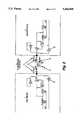
- FIG. 1is a block diagram of the transceiver circuits for each device of the present invention showing the interconnection between the devices across the isolation barrier of the interface.
- FIG. 2is a detailed circuit diagram of the present invention showing the use of a pulse transformer as the isolation barrier.
- FIG. 3is a detailed circuit diagram of the present invention showing the use of a capacitative coupling as the isolation barrier.
- FIG. 4is a timing chart diagram for describing the operation of the circuits of the present invention.
- FIG. 5is a block diagram showing the implementation of the present invention between the LLC and PHY chips pursuant to the IEEE P1394 specification.
- the present inventionrelates to a method and apparatus for the transmission of data signals across an interface comprising an isolation barrier disposed between adjacent devices connected via a bus.
- numerous detailsare set forth such as voltages, currents, device types, etc., in order to provide a thorough understanding of the present invention. It will be obvious, however, to one skilled in the art that these details are not required to practice the present invention. In other instances, well-known circuits, methods and the like are not set forth in detail in order to avoid unnecessarily obscuring the present invention.
- the present inventioncomprises a first device 1 and a second device 2 interconnected across an interface 3 by means of a bus 20.
- the bus 20comprises at least one transmission line 21 for transmitting data and control signals and further comprises an isolation barrier 9 coupled to the transmission lines 21 for electrically isolating the transmitting and receiving circuitry of the two devices 1 and 2 to prevent ground loops therebetween.
- Blocking capacitors 11of approximately 0.001 ⁇ f are coupled to the transmission lines 21 of the bus 20 on each side of the isolation barrier 9 to prevent DC current from being supplied to the isolation barrier 9.
- the series resistors 8are disposed on respective sides of the isolation barrier 9 to provide signal voltage attenuation and current limiting in order to protect the input diodes (not shown) of each device 1 and 2.
- the shunt resistor 10determines the amount of voltage attenuation and acts to help discharge the pin capacitance of each device 1 and 2 when their drivers 6 are tri-stated.
- the values for the components described abovehave been chosen for transmission rates on the bus of approximately 50 Megabits/second so that for different transmission rates, these values would have to be modified as is well-known in the art.
- the interface 3 between the devicesis half duplex, bi-directional such that each device 1 and 2 comprises a transceiver having a transmitter or driver 6 consisting of a tri-state gate and a receiver 12 consisting of a Schmidt trigger.
- the isolation barrier 9comprises a pulse transformer 9 (of 80 ⁇ H) for galvanic isolation of the circuitry of each device 1 and 2 as is well-known in the art.
- the method and apparatus of the present inventionwill be explained in terms of the transmitter 6 of the first device 1 transmitting the transmission signal to the receiver 12 of the second device 2 where it is reconstituted into the original data signal input to the circuitry of the first device 1.
- the present inventionis applicable to uni-directional interfaces 3 and to isolation barriers 9 other than pulse transformers 9 and capacitative couplings (shown in FIG. 3).
- an NRZ input data signal A having digital high and low valuesis generated from a memory read, a peripheral input device or the like.
- this data signal Ais supplied to a data synchronizer 4 consisting of a first D-Q flip-flop 13 for synchronizing the data signal A with a clock signal also input to the first D-Q flip flop 13.
- the synchronized data signal B derived therefromis supplied along with the clock signal to a digital differentiator 5 for differentiating the pulses of the data signal A.
- the digital differentiator 5may comprise a second flip-flop 14 for receiving the synchronized data signal B and the clock signal and outputting a delayed data signal C.
- This delayed data signal Cis next supplied as input along with the synchronized data signal B to an exclusive OR gate 15.
- the exclusive OR gate 15senses both the positive and negative transitions of the pulses in the synchronized data signal B and outputs as the digitally differentiated signal D a series of pulses corresponding to these transitions.
- the synchronized data signal Bis supplied as a first (data) input to a transmitter 6 or driver 6 consisting of a tri-state gate 6.
- the tri-state gate 6also receives as a second (control) input the digitally differentiated signal D which enables the gate 6 when high and disables the gate when low.
- a bias voltage 16is applied to the output of the tri-state gate 6 to maintain the output of the gate 6 at an intermediate state of approximately 2.5 volts when the gate 6 is disabled.
- the bias voltage 16is generated by a tied back inverter 16, which in some instances, may require two pins in order to connect the input to the output. It is also permissible to set the bias voltage 16 used in the present invention in other ways, such as with an external resistor voltage divider having 5K ⁇ resistors.
- a first intermediate transmission signal E as the output of the gate 6is driven on the bus 20 and transmitted across the isolation barrier 9.
- the gate 6is then enabled, in which case, if the synchronized data signal B is also high, a first high transmission signal E as the output of the gate 6 is driven onto the bus.
- This first high transmission signal Ecomprises a high state of approximately 5 volts.
- a first low transmission signal Eis driven onto the bus 20.
- This first low transmission signal Ecomprises a low state of approximately 0 volts.
- the transmitter circuitry of the first device 1converts the NRZ input data signal A into a DC balanced transmission signal E (without increasing the signal's high frequency bandwidth) that can be effectively transmitted across the isolation barrier 9.
- the foregoing signal amplitudesmay vary (i.e., higher or lower) depending upon the specific bias voltage 16 utilized and the specifications of the particular electronic components also used.
- the first transmission signal EWhen the first transmission signal E is driven onto the bus, it is received as 0 volt DC input to the pulse transformer 9.
- the transformer 9magnetically couples this signal to the bus 20 on the opposite side adjacent to the second device 2 where the output is a second transmission signal F.
- the second transmission signal Fis substantially the same as the first transmission signal E except that it varies in amplitude therefrom.
- This second transmission signal Fis then received as input to a receiver 12 of the second device 2 consisting of a Schmidt trigger 12.
- the Schmidt trigger 12reconstitutes the non-return to zero data of the second transmission signal F into the digital pulses of the synchronized data signal B originally received as input to the digital differentiator 5.
- the Schmidt trigger 12comprises two threshold voltages centered around the bias voltage 16, preferably having the values of 2 volts and 3 volts, where 3 volts is the threshold for rising edges and 2 volts is the threshold for falling edges which cause the Schmidt trigger 12 to go high and low, respectively.
- the output of the Schmidt trigger 12is therefore a series of high and low transitions which in effect reconstitutes the synchronized data signal B.
- any electronic componentcan be utilized which has as an output a high data signal when the voltage of its input signal reaches a value substantially above the voltage bias 16, and a low data signal when the input signal reaches a value substantially below the voltage bias.
- Another embodiment of the method and apparatus of the present inventionis designed specifically for implementation with the multi-speed bus architecture scheme described in IEEE PG,16 Standards Document P1394 entitled "High Performance Serial Bus".
- the bus architecture scheme described in P1394is intended to provide a multi-speed, serial bus 20 having a low cost, universal interconnection between cards on the same backplane, cards on other backplanes, and external peripherals. It also provides for an arbitrary bus topology where devices or nodes (i.e. addressable devices coupled to the bus having a minimum set of control registers) coupled to the bus 20 need not be arranged in a cyclic network but can be arbitrarily coupled to other device 5 via the serial bus 20 to form an assorted number of network arrangements.
- the multi-speed serial bus 20comprising a twisted pair cable 20 is provided for universal interconnection between computer devices arbitrarily configured on the bus.
- Each device 1 and 2comprises a physical channel interface chip (or “PHY” chip) 25 directly connected to the serial bus 20 for arbitrating, transmitting, receiving and re-timing of the data signals.
- Each devicesimilarly comprises a link layer chip (or "LLC” chip) 24 which transmits and receives the data signals at a fixed speed to and from the PHY chip 25 and interfaces with the processing intelligence of the device.
- the fixed speed transmission between the two chips 24 and 25is enabled by a conversion process whereby the bus 20 between the two chips 24 and 25 becomes wider (i.e. more transmission channels are used) for faster data signal transmissions.
- the bus 20must be at least two bits wide; for a 200 Mbit transmission, the bus must 20 at least four bits wide; for a 400 Mbit transmission, the bus 20 must be at least eight bits wide; and so on.
- the interface 3 of the present inventioncomprising the isolation barrier 9 is implemented between the PHY and LLC chips 24 and 25 so as to permit the development of a universal interconnection in which a standard serial bus cable 20 can be connected between the PHY chips 25 of adjacent devices 1 and 2.
- the signals transmittedare in the form of NRZ data signals which require very broad band transmission capabilities. Due to the fact that a pulse transformer 9 having a narrow band transmission channel is implemented as the isolation barrier 9, it is necessary that the transmitting and receiving circuitry of the PHY and LLC chips 24 and 25 convert the data signals into narrow band data signals for transmission between the PHY and LLC chips 24 and 25. Therefore, according to the method and apparatus of the present invention, the circuitry described above is implemented between the PHY and LLC chips so as to provide a simple method using digital standard cell or gate array technology in a standard digital CMOS process to pass the NRZ data signals across the isolation barrier 9 of the interface 3 disposed between the two chips 24 and 25.
- the interface 3may be uni-directional or bi-directional and may represent the communications channel between two separate devices 1 and 2, two IC chips 24 and 25 or the like.
- the isolation barrier 9 coupled to the bus in the interfacemay comprise a variety of devices or configurations which electrically isolate the transmitting and receiving circuitry of the two devices 1 and 2.
Landscapes
- Engineering & Computer Science (AREA)
- Theoretical Computer Science (AREA)
- General Engineering & Computer Science (AREA)
- Physics & Mathematics (AREA)
- Signal Processing (AREA)
- Computer Networks & Wireless Communication (AREA)
- Computer Hardware Design (AREA)
- General Physics & Mathematics (AREA)
- Spectroscopy & Molecular Physics (AREA)
- Power Engineering (AREA)
- Dc Digital Transmission (AREA)
- Bus Control (AREA)
- Logic Circuits (AREA)
- Small-Scale Networks (AREA)
Abstract
Description
The present invention relates to a bus architecture communications scheme for enabling communications between a plurality nodes or devices in a computer system. More particularly, the present invention relates to an interface between two devices connected via the bus in which binary signals in the form of NRZ data signals are transmitted through an isolation barrier disposed between the two devices.
Computer devices within a given computer system, such as a microprocessor, a disk drive, a CRT, a printer and the like, need the ability to convey signals between themselves. In the electronics and computer fields, this has been accomplished by means of a bus which comprises a plurality of transmission wires and acts as a communications path for interconnecting several devices in the system. Each device of the system need only plug into the bus to be theoretically connected to each of the other devices in the system. In order to communicate with other devices attached to the bus, each must be equipped with hardware such as transmitting and receiving circuitry compatible with the communications protocol implemented for the bus. However, due to the small signal voltages and currents driven on the bus by each of the above-circuits, a means of electrical or galvanic isolation must be implemented between the circuits. This isolation reduces system ground loop currents and prevents ground drops from interfering with the signal transmission. In conventional bus architectures, one way to electrically isolate the circuitries connected to the bus is to place a pulse transformer in a module at the end of a cable (comprising the bus) to be attached to an associated device.
However, a major drawback in the use of a pulse transformer implemented as the isolation barrier is that it acts as a high pass filter due to the fact that pulse transformers only AC couple the input to the output. If the transmitter drives a high signal on the bus for a prolonged period, the signal as seen by the receiver begins to fall due to the high pass filtering. Hence, not all the data in a broad band spectrum NRZ data signal is transmitted through the narrow band channel created by the pulse transformer because of the unrecoverable loss of the lower band data.
Currently, there are several techniques of passing broad band NRZ data signals through a narrow band channel. One such technique consists of analog and digital modulation wherein a carrier wave is used to transmit broad band data on a specific frequency. However, this technique is relatively complicated, requiring a significant amount of hardware which increases costs and generally requires circuits not available in standard cell gate array technology.
Another prior art transmission technique provides for encoding of the NRZ data signal at the transmitting end of the cable and decoding of the data signal at the receiving end of the cable. This is typically performed by Manchester, 4B5B, 8B10B, etc. encoding of the data signal in which a balanced code is maintained so as to provide an essentially constant DC level. For example, Manchester is a bit level balanced code in which the DC level from bit to bit does not change, while 4B5B and 8B10B are byte level balanced codes in which the DC level of a byte changes by less than 10 to 20%. However, such encoding techniques increase the bandwidth of the NRZ data signal. As an example, when a 50 Megabit Manchester encoded signal is transmitted across the isolation barrier, the bandwidth of the signal is in the range of 20 to 50 MHz rather than the original NRZ spectrum of DC to 25 MHz. Furthermore, a significant amount of electronic hardware is required to implement these coding techniques, thereby increasing the cost and reducing the performance (i.e. higher bit error rates) of the overall bus architecture.
In addition to the foregoing, another drawback in the use of prior art transmission methods and apparatus is that they are based upon typical bus architecture schemes, such as SCSI, Ethernet and ADB, which do not provide for multi-speed signal transmissions on an upward compatible bus where the capabilities of faster devices connected to such a multi-speed bus can be realized.
Accordingly, it is an object of the present invention to provide a method and apparatus for the transmission of NRZ data signals across an isolation barrier disposed between adjacent devices on a bus.
Another object of the present invention is to provide a method and apparatus for transmitting broad band NRZ data signals across a pulse transformer type isolation barrier having a narrow band channel.
A further object of the present invention is to implement the method and apparatus of the present invention in a multi-speed bus architecture scheme using digital standard cell or gate array technology so as to transmit NRZ data signals across a bi-directional interface between adjacent devices coupled to the bus.
The present invention provides a method and apparatus for the transmission of data signals across an interface comprising an isolation barrier disposed between first and second devices connected via a bus. The isolation barrier may comprise a pulse transformer, a capacitative coupling or the like for electrically isolating the transmitting and receiving circuitry of the devices and to prevent ground loops therebetween.
In the first device, an NRZ input data signal is supplied to a data synchronizer for synchronizing the data signal with a clock signal also input to the data synchronizer. The synchronized data signal derived therefrom is supplied along with the clock signal to a differentiator for differentiating the pulses of the data signal and outputting a delayed data signal which is next supplied as input to a driver consisting of a tri-state gate.
The tri-state gate also receives as a second (control) input the digitally differentiated signal which enables the gate when high and disables the gate when low. A bias voltage is applied to the output of the tri-state gate to maintain the output of the gate at an intermediate state when the gate is disabled. When the differentiated signal goes high, the gate is enabled, in which case, if the synchronized data signal is also high, a high transmission signal as the output of the gate is driven onto the bus. If the gate is enabled and the input synchronized data signal goes low, then a low transmission signal is driven onto the bus. In this manner, the transmitter circuitry of the first device converts the NRZ input data signal into a DC balanced transmission signal that can be effectively transmitted across the isolation barrier.
A Schmidt trigger is provided as the receiver of the second device and comprises two threshold voltages centered around the bias voltage. The Schmidt trigger receivers the signal transmitted across the isolation barrier and outputs a series of high and low transitions which in effect reconstitutes the synchronized data signal.
In addition to the foregoing description, another embodiment of the present invention is designed specifically for implementation with the multi-speed bus architecture scheme described in IEEE Standards Document P1394 entitled "High Performance Serial Bus". The multi-speed serial bus comprising a twisted pair cable is provided for universal interconnection between computer devices arbitrarily configured on the bus. In this embodiment, the interface of the present invention comprising the isolation barrier is implemented between physical interface chip and the link layer chip of the bus architecture scheme set forth in the P1394 standard. The method and apparatus of the present invention is implemented between the two chips so as to provide a simple method using digital standard cell or gate array technology in a standard digital CMOS process to pass the NRZ data signals across the isolation barrier disposed between the two chips.
The objects, features and advantages of the present invention will become apparent from the following detailed description of the preferred embodiment in which:
FIG. 1 is a block diagram of the transceiver circuits for each device of the present invention showing the interconnection between the devices across the isolation barrier of the interface.
FIG. 2 is a detailed circuit diagram of the present invention showing the use of a pulse transformer as the isolation barrier.
FIG. 3 is a detailed circuit diagram of the present invention showing the use of a capacitative coupling as the isolation barrier.
FIG. 4 is a timing chart diagram for describing the operation of the circuits of the present invention.
FIG. 5 is a block diagram showing the implementation of the present invention between the LLC and PHY chips pursuant to the IEEE P1394 specification.
The present invention relates to a method and apparatus for the transmission of data signals across an interface comprising an isolation barrier disposed between adjacent devices connected via a bus. In the following description, numerous details are set forth such as voltages, currents, device types, etc., in order to provide a thorough understanding of the present invention. It will be obvious, however, to one skilled in the art that these details are not required to practice the present invention. In other instances, well-known circuits, methods and the like are not set forth in detail in order to avoid unnecessarily obscuring the present invention.
With reference to FIGS. 1 and 2, the present invention comprises afirst device 1 and asecond device 2 interconnected across aninterface 3 by means of abus 20. Thebus 20 comprises at least onetransmission line 21 for transmitting data and control signals and further comprises anisolation barrier 9 coupled to thetransmission lines 21 for electrically isolating the transmitting and receiving circuitry of the twodevices Blocking capacitors 11 of approximately 0.001 μf are coupled to thetransmission lines 21 of thebus 20 on each side of theisolation barrier 9 to prevent DC current from being supplied to theisolation barrier 9. In addition, as shown in FIGS. 1 and 2, three resistors, two series resistors 8 of approximately 100Ω and athird shunt resistor 10 of approximately 300Ω (which is connected to ground to shunt the pulse transformer 9), are further coupled to thetransmission lines 21 of thebus 20. The series resistors 8 are disposed on respective sides of theisolation barrier 9 to provide signal voltage attenuation and current limiting in order to protect the input diodes (not shown) of eachdevice shunt resistor 10 determines the amount of voltage attenuation and acts to help discharge the pin capacitance of eachdevice drivers 6 are tri-stated. The values for the components described above have been chosen for transmission rates on the bus of approximately 50 Megabits/second so that for different transmission rates, these values would have to be modified as is well-known in the art.
According to one embodiment of the present invention, theinterface 3 between the devices is half duplex, bi-directional such that eachdevice driver 6 consisting of a tri-state gate and areceiver 12 consisting of a Schmidt trigger. Furthermore, according to this embodiment, theisolation barrier 9 comprises a pulse transformer 9 (of 80 μH) for galvanic isolation of the circuitry of eachdevice transmitter 6 of thefirst device 1 transmitting the transmission signal to thereceiver 12 of thesecond device 2 where it is reconstituted into the original data signal input to the circuitry of thefirst device 1. Due to the bi-directional nature of theinterface 3, the configuration of elements and their operation are identical for each device. However, the present invention is applicable touni-directional interfaces 3 and toisolation barriers 9 other thanpulse transformers 9 and capacitative couplings (shown in FIG. 3).
In thefirst device 1, an NRZ input data signal A having digital high and low values is generated from a memory read, a peripheral input device or the like. As shown in FIG. 1 and more specifically in FIG. 2, this data signal A is supplied to adata synchronizer 4 consisting of a first D-Q flip-flop 13 for synchronizing the data signal A with a clock signal also input to the first D-Qflip flop 13. The synchronized data signal B derived therefrom is supplied along with the clock signal to adigital differentiator 5 for differentiating the pulses of the data signal A. As shown in FIG. 2, thedigital differentiator 5 may comprise a second flip-flop 14 for receiving the synchronized data signal B and the clock signal and outputting a delayed data signal C. This delayed data signal C is next supplied as input along with the synchronized data signal B to an exclusive ORgate 15. With reference to the signals B and C shown in the timing chart of FIG. 3, the exclusive ORgate 15 senses both the positive and negative transitions of the pulses in the synchronized data signal B and outputs as the digitally differentiated signal D a series of pulses corresponding to these transitions.
Now referring to both FIGS. 1 and 2, the synchronized data signal B is supplied as a first (data) input to atransmitter 6 ordriver 6 consisting of atri-state gate 6. Thetri-state gate 6 also receives as a second (control) input the digitally differentiated signal D which enables thegate 6 when high and disables the gate when low. Abias voltage 16 is applied to the output of thetri-state gate 6 to maintain the output of thegate 6 at an intermediate state of approximately 2.5 volts when thegate 6 is disabled. As shown in FIG. 2, thebias voltage 16 is generated by a tied backinverter 16, which in some instances, may require two pins in order to connect the input to the output. It is also permissible to set thebias voltage 16 used in the present invention in other ways, such as with an external resistor voltage divider having 5KΩ resistors.
When thegate 6 is disabled, a first intermediate transmission signal E as the output of thegate 6 is driven on thebus 20 and transmitted across theisolation barrier 9. When the digitally differentiated signal D goes high, thegate 6 is then enabled, in which case, if the synchronized data signal B is also high, a first high transmission signal E as the output of thegate 6 is driven onto the bus. This first high transmission signal E comprises a high state of approximately 5 volts. However, if thegate 6 is enabled and the input synchronized data signal B goes low, then a first low transmission signal E is driven onto thebus 20. This first low transmission signal E comprises a low state of approximately 0 volts. Therefore, the transmitter circuitry of thefirst device 1 converts the NRZ input data signal A into a DC balanced transmission signal E (without increasing the signal's high frequency bandwidth) that can be effectively transmitted across theisolation barrier 9. As would be obvious to one skilled in the art, the foregoing signal amplitudes may vary (i.e., higher or lower) depending upon thespecific bias voltage 16 utilized and the specifications of the particular electronic components also used.
When the first transmission signal E is driven onto the bus, it is received as 0 volt DC input to thepulse transformer 9. Thetransformer 9 magnetically couples this signal to thebus 20 on the opposite side adjacent to thesecond device 2 where the output is a second transmission signal F. As can be seen from the timing chart of FIG. 4, the second transmission signal F is substantially the same as the first transmission signal E except that it varies in amplitude therefrom. This second transmission signal F is then received as input to areceiver 12 of thesecond device 2 consisting of aSchmidt trigger 12. The Schmidt trigger 12 reconstitutes the non-return to zero data of the second transmission signal F into the digital pulses of the synchronized data signal B originally received as input to thedigital differentiator 5.
The Schmidt trigger 12 comprises two threshold voltages centered around thebias voltage 16, preferably having the values of 2 volts and 3 volts, where 3 volts is the threshold for rising edges and 2 volts is the threshold for falling edges which cause theSchmidt trigger 12 to go high and low, respectively. With reference to the timing chart of FIG. 4, the output of theSchmidt trigger 12 is therefore a series of high and low transitions which in effect reconstitutes the synchronized data signal B. However, as an alternative to aSchmidt trigger 12, it is noted that any electronic component can be utilized which has as an output a high data signal when the voltage of its input signal reaches a value substantially above thevoltage bias 16, and a low data signal when the input signal reaches a value substantially below the voltage bias.
In addition to the foregoing description, another embodiment of the method and apparatus of the present invention is designed specifically for implementation with the multi-speed bus architecture scheme described in IEEE PG,16 Standards Document P1394 entitled "High Performance Serial Bus". This document is appended hereto as Appendix A for reference. The bus architecture scheme described in P1394 is intended to provide a multi-speed,serial bus 20 having a low cost, universal interconnection between cards on the same backplane, cards on other backplanes, and external peripherals. It also provides for an arbitrary bus topology where devices or nodes (i.e. addressable devices coupled to the bus having a minimum set of control registers) coupled to thebus 20 need not be arranged in a cyclic network but can be arbitrarily coupled toother device 5 via theserial bus 20 to form an assorted number of network arrangements.
In this embodiment, as shown in FIG. 5, the multi-speedserial bus 20 comprising atwisted pair cable 20 is provided for universal interconnection between computer devices arbitrarily configured on the bus. Eachdevice serial bus 20 for arbitrating, transmitting, receiving and re-timing of the data signals. Each device similarly comprises a link layer chip (or "LLC" chip) 24 which transmits and receives the data signals at a fixed speed to and from thePHY chip 25 and interfaces with the processing intelligence of the device. The fixed speed transmission between the twochips bus 20 between the twochips bus 20 must be at least two bits wide; for a 200 Mbit transmission, the bus must 20 at least four bits wide; for a 400 Mbit transmission, thebus 20 must be at least eight bits wide; and so on. In this embodiment, theinterface 3 of the present invention comprising theisolation barrier 9 is implemented between the PHY andLLC chips serial bus cable 20 can be connected between the PHY chips 25 ofadjacent devices
In this implementation, the signals transmitted are in the form of NRZ data signals which require very broad band transmission capabilities. Due to the fact that apulse transformer 9 having a narrow band transmission channel is implemented as theisolation barrier 9, it is necessary that the transmitting and receiving circuitry of the PHY andLLC chips LLC chips isolation barrier 9 of theinterface 3 disposed between the twochips
While the present invention has been described in conjunction with the above-embodiments, it is evident that numerous alternatives, depictions, variations and uses will be apparent to those skilled in the art in light of the foregoing description. Specifically, theinterface 3 may be uni-directional or bi-directional and may represent the communications channel between twoseparate devices IC chips isolation barrier 9 coupled to the bus in the interface may comprise a variety of devices or configurations which electrically isolate the transmitting and receiving circuitry of the twodevices
Claims (7)
1. A method for transmitting an NRZ data signal across an interface between two devices interconnected via a bus, the method comprising the steps of:
differentiating the data signal with a signal differentiator responsive to a clock signal to produce a differentiated signal;
supplying the data signal as a first input to a driver comprising a tri-state gate;
supplying the differentiated signal as a second input to the tri-state gate to enable the tri-state gate when the differentiated signal is high;
applying a bias voltage to an output of the tri-state gate to derive as output from the tri-state gate a transmission signal for transmission across the interface;
transmitting the transmission signal across the interface between the two devices; and
supplying the transmission signal as input to an electronic component having as output a reconstituted data signal comprising
(1) a high data signal when the input to the electronic component reaches a value substantially above the voltage bias, and
(2) a low data signal when the input to the electronic component reaches a value substantially below the voltage bias.
2. A method for transmitting an NRZ data signal across an interface comprising an isolation barrier disposed between a first device and a second device interconnected via a bus, the method comprising the steps of:
differentiating the data signal with a signal differentiator responsive to the clock signal to produce a differentiated signal;
supplying the data signal as a first input to a driver comprising a tri-state gate;
supplying the differentiated signal as a second input to the tri-state gate to enable the tri-state gate when the differentiated signal is high;
applying a bias voltage to an output of the tri-state gate to derive as output from the tri-state gate a transmission signal comprising
(1) an intermediate transmission signal corresponding to the voltage bias when the tri-state gate is disabled,
(2) a high transmission signal when the tri-state gate is enabled and the first input to the tri-state gate is high, and
(3) a low transmission signal when the tri-state gate is enabled and the first input to the tri-state gate is low;
transmitting the transmission signal derived from the output of the tri-state gate from the first device through the isolation barrier to the second device; and
supplying the transmission signal to a Schmidt trigger to derive as output from the Schmidt trigger a reconstituted data signal corresponding to the data signal.
3. A method for transmitting an NRZ data signal across an interface comprising an isolation barrier disposed between a first device and a second device interconnected via a bus, the method comprising the steps of:
synchronizing the data signal with a clock signal;
supplying the synchronized data signal to a flip-flop responsive to the clock signal to output a delayed synchronized data signal delayed by one clock period;
supplying the synchronized data signal as a first input to an exclusive OR gate;
supplying the delayed synchronized data signal as a second input to the exclusive OR gate to output a differentiated signal;
supplying the synchronized data signal as a first input to a driver comprising a tri-state gate;
supplying the differentiated signal as a second input to the tri-state gate to enable the tri-state gate when the differentiated signal is high;
applying a bias voltage to an output of the tri-state gate to derive as output from the tri-state gate a first transmission signal comprising
(1) an intermediate transmission signal corresponding to the bias voltage when the tri-state gate is disabled,
(2) a high transmission signal when the tri-state gate is enabled and the first input to the tri-state gate is high, and
(3) a low transmission signal when the tri-state gate is enabled and the first input to the tri-state gate is low;
transmitting the first transmission signal derived from the output of the tri-state gate from the first device to the isolation barrier to generate as output from the isolation barrier a second transmission signal electrically isolated from the first transmission signal; and
transmitting the second transmission signal to a Schmidt trigger having two thresholds to derive as output from the Schmidt trigger a reconstituted data signal corresponding to the synchronized data signal, wherein the bias voltage applied to the output of the tri-state gate sets a DC level of the first and second transmission signals around which a voltage difference between the thresholds of the Schmidt trigger is centered.
4. The method according to claim 3, wherein the step of transmitting the first transmission signal to the isolation barrier further comprises the step of transmitting the first transmission signal through a first blocking capacitor and a first resistor before reception of the first transmission signal by the isolation barrier, and wherein the step of transmitting the second transmission signal to the Schmidt trigger further comprises the step of transmitting the second transmission signal through a second blocking capacitor and a second resistor before reception of the second transmission signal by the Schmidt trigger.
5. An apparatus for transmitting an NRZ data signal across an interface between two devices interconnected via a bus, the apparatus comprising:
a signal differentiator responsive to a clock signal for receiving the data signal and outputting a differentiated signal;
a driver comprising a tri-state gate having as a first input the data signal, the tri-state gate further having as a second input the differentiated signal for enabling the tri-gate when the differentiated signal is high;
a bias voltage applied to an output of the tri-state gate to derive as output from the tri-state gate a transmission signal for transmission via the bus across the interface between the two devices; and
an electronic component for receiving the transmission signal and outputting a reconstituted data signal comprising
(1) a high data signal when the input to the electronic component reaches a value substantially above the voltage bias, and
(2) a low data signal when the input to the electronic component reaches a value substantially below the voltage bias.
6. An apparatus for transmitting an NRZ data signal across an interface comprising an isolation barrier disposed between a first device and a second device interconnected via a bus, the apparatus comprising:
a first flip-flop responsive to a clock signal for receiving the data signal and outputting a synchronized data signal;
a second flip-flop responsive to the clock signal for receiving the synchronized data signal and outputting a delayed synchronized data signal delayed by one clock period;
an exclusive OR gate for receiving as input the delayed synchronized data signal and the synchronized data signal and outputting a differentiated signal;
a tri-state gate for receiving as a first input the synchronized data signal and receiving as a second input the differentiated signal, the differentiated signal enabling the tri-state gate when the differentiated signal is high;
a bias voltage applied to an output of the tri-state gate for outputting a first transmission signal comprising
(1) an intermediate transmission signal corresponding to the bias voltage when the tri-state gate is disabled,
(2) a high transmission signal when the tri-state gate is enabled and the first input to the tri-state gate is high, and
(3) a low transmission signal when the tri-state gate is enabled and the first input to the tri-state gate is low;
a first blocking capacitor disposed in the bus between the first device and the isolation barrier;
a first resistor disposed in the bus between the first blocking capacitor and the isolation barrier;
the isolation barrier for receiving the first transmission signal and outputting a second transmission signal electrically isolated from the first transmission signal;
a second resistor disposed in the bus between the isolation barrier and the second device;
a second blocking capacitor disposed in the bus between the second resistor and the second device; and
a Schmidt trigger for receiving as input the second transmission signal and outputting a reconstituted data signal corresponding to the synchronized data signal.
7. A method for transmitting an NRZ data signal across an interface between two devices interconnected via a bus, the method comprising the steps of:
differentiating the data signal with a signal differentiator responsive to a clock signal to produce a differentiated signal having a first state and a second state;
supplying the data signal as a first input to a driver comprising a tri-state gate;
supplying the differentiated signal as a second input to the tri-state gate to enable the tri-state gate when the differentiated signal is in the first state;
applying a bias voltage to an output of the tri-state gate to derive as output from the tri-state gate a transmission signal for transmission across the interface;
transmitting the transmission signal across the interface between the two devices; and
supplying the transmission signal as input to an electronic component having as output a reconstituted data signal comprising
(1) a first signal corresponding to a first logic state when the input to the electronic component reaches a value substantially above the voltage bias, and
(1) a second signal corresponding to a second logic state when the input to the electronic component reaches a value substantially below the voltage bias.
Priority Applications (13)
| Application Number | Priority Date | Filing Date | Title |
|---|---|---|---|
| US07/999,155US5384808A (en) | 1992-12-31 | 1992-12-31 | Method and apparatus for transmitting NRZ data signals across an isolation barrier disposed in an interface between adjacent devices on a bus |
| CA002151373ACA2151373C (en) | 1992-12-31 | 1993-12-16 | Method and apparatus for transmitting nrz data signals across an isolation barrier disposed in an interface between adjacent devices on a bus |
| CA002365604ACA2365604C (en) | 1992-12-31 | 1993-12-16 | Method and apparatus for transmitting nrz data signals across an isolation barrier disposed in an interface between adjacent devices on a bus |
| DE69332804TDE69332804T2 (en) | 1992-12-31 | 1993-12-16 | METHOD AND DEVICE FOR THE NRZ DATA SIGNAL TRANSMISSION BY AN INSULATION BARRIER IN A INTERFACE BETWEEN NEIGHBOR DEVICES ON A BUS |
| CA002415289ACA2415289C (en) | 1992-12-31 | 1993-12-16 | Method and apparatus for transmitting nrz data signals across an isolation barrier disposed in an interface between adjacent devices on a bus |
| EP94905427AEP0677191B1 (en) | 1992-12-31 | 1993-12-16 | Method and apparatus for transmitting nrz data signals across an isolation barrier disposed in an interface between adjacent devices on a bus |
| PCT/US1993/012324WO1994016390A1 (en) | 1992-12-31 | 1993-12-16 | Method and apparatus for transmitting nrz data signals across an isolation barrier disposed in an interface between adjacent devices on a bus |
| DE69334202TDE69334202T2 (en) | 1992-12-31 | 1993-12-16 | A method and apparatus for transmitting NRZ data signals through an isolation barrier in an interface between neighboring devices on a bus |
| EP02008694AEP1306765B1 (en) | 1992-12-31 | 1993-12-16 | Method and apparatus for transmitting nrz data signals across an isolation barrier disposed in an interface between adjacent devices on a bus |
| KR1019950702714AKR960700480A (en) | 1992-12-31 | 1993-12-16 | METHOD AND APPARATUS FOR TRANSMITTING NRZ DATA SIGNALS ACROSS AN ISOLATION BARRIER DISPOSED IN AN INTERFACE BETWEEN ADJACENT DEVICES ON A BUS |
| JP51601894AJP3399950B2 (en) | 1992-12-31 | 1993-12-16 | Method and apparatus for transmitting an NRZ data signal through an isolation barrier provided at an interface between adjacent devices on a bus |
| AU59544/94AAU5954494A (en) | 1992-12-31 | 1993-12-16 | Method and apparatus for transmitting nrz data signals across an isolation barrier disposed in an interface between adjacent devices on a bus |
| HK03104168.5AHK1052063B (en) | 1992-12-31 | 2003-06-11 | Method and apparatus for transmitting nrz data signals across an isolation barrier disposed in an interface between adjacent devices on a bus |
Applications Claiming Priority (1)
| Application Number | Priority Date | Filing Date | Title |
|---|---|---|---|
| US07/999,155US5384808A (en) | 1992-12-31 | 1992-12-31 | Method and apparatus for transmitting NRZ data signals across an isolation barrier disposed in an interface between adjacent devices on a bus |
Publications (1)
| Publication Number | Publication Date |
|---|---|
| US5384808Atrue US5384808A (en) | 1995-01-24 |
Family
ID=25545970
Family Applications (1)
| Application Number | Title | Priority Date | Filing Date |
|---|---|---|---|
| US07/999,155Expired - LifetimeUS5384808A (en) | 1992-12-31 | 1992-12-31 | Method and apparatus for transmitting NRZ data signals across an isolation barrier disposed in an interface between adjacent devices on a bus |
Country Status (8)
| Country | Link |
|---|---|
| US (1) | US5384808A (en) |
| EP (2) | EP0677191B1 (en) |
| JP (1) | JP3399950B2 (en) |
| KR (1) | KR960700480A (en) |
| AU (1) | AU5954494A (en) |
| CA (1) | CA2151373C (en) |
| DE (2) | DE69332804T2 (en) |
| WO (1) | WO1994016390A1 (en) |
Cited By (152)
| Publication number | Priority date | Publication date | Assignee | Title |
|---|---|---|---|---|
| US5654984A (en)* | 1993-12-03 | 1997-08-05 | Silicon Systems, Inc. | Signal modulation across capacitors |
| EP0801468A2 (en)* | 1996-04-08 | 1997-10-15 | Texas Instruments Inc. | Improvements in or relating to integrated circuits |
| US5787120A (en)* | 1995-01-30 | 1998-07-28 | Alcatel N.V. | Transmission method and transmitter for signals with a decoupled low level and at least one coupled high level for a telecommunication network including such a transmitter |
| WO1998037672A1 (en)* | 1997-02-21 | 1998-08-27 | Analog Devices, Inc. | Logic isolator with high transient immunity |
| US5917364A (en)* | 1996-12-25 | 1999-06-29 | Nec Corporation | Bi-directional interface circuit of reduced signal alteration |
| US5936429A (en)* | 1996-09-19 | 1999-08-10 | Oki Electric Industry Co., Ltd. | Interface circuit and method for transmitting binary logic signals with reduced power dissipation |
| WO1999066414A1 (en)* | 1998-06-16 | 1999-12-23 | Modubility Llc | Modular mobile computer system |
| EP0977406A1 (en)* | 1998-07-17 | 2000-02-02 | Endress + Hauser Wetzer GmbH + Co. KG | Circuit for transmission of galvanically isolated digital signals |
| US6061009A (en)* | 1998-03-30 | 2000-05-09 | Silicon Laboratories, Inc. | Apparatus and method for resetting delta-sigma modulator state variables using feedback impedance |
| US6064326A (en)* | 1998-03-30 | 2000-05-16 | Silicon Laboratories, Inc. | Analog-to-digital conversion overload detection and suppression |
| US6078205A (en)* | 1997-03-27 | 2000-06-20 | Hitachi, Ltd. | Circuit device, drive circuit, and display apparatus including these components |
| US6104794A (en)* | 1997-04-22 | 2000-08-15 | Silicon Laboratories, Inc. | Architecture for minimum loop current during ringing and caller ID |
| US6107948A (en)* | 1997-04-22 | 2000-08-22 | Silicon Laboratories, Inc. | Analog isolation system with digital communication across a capacitive barrier |
| US6115764A (en)* | 1994-09-27 | 2000-09-05 | International Business Machines Corporation | Acyclic cable bus having redundant path access |
| US6137827A (en)* | 1997-04-22 | 2000-10-24 | Silicon Laboratories, Inc. | Isolation system with digital communication across a capacitive barrier |
| US6144326A (en)* | 1997-04-22 | 2000-11-07 | Silicon Laboratories, Inc. | Digital isolation system with ADC offset calibration |
| US6160885A (en)* | 1997-04-22 | 2000-12-12 | Silicon Laboratories, Inc. | Caller ID circuit powered through hookswitch devices |
| US6167134A (en)* | 1997-04-22 | 2000-12-26 | Silicon Laboratories, Inc. | External resistor and method to minimize power dissipation in DC holding circuitry for a communication system |
| US6167132A (en)* | 1997-04-22 | 2000-12-26 | Silicon Laboratories, Inc. | Analog successive approximation (SAR) analog-to-digital converter (ADC) |
| US6166575A (en)* | 1997-08-20 | 2000-12-26 | Advantest Corporation | Signal transmission circuit achieving significantly improved response time of a driven circuit, CMOS semiconductor device and circuit board therefor |
| US6198816B1 (en) | 1997-04-22 | 2001-03-06 | Silicon Laboratories, Inc. | Capacitively coupled ring detector with power provided across isolation barrier |
| US6201865B1 (en) | 1997-04-22 | 2001-03-13 | Silicon Laboratories, Inc. | Digital access arrangement circuitry and method for connecting to phone lines having a DC holding circuit with switchable time constants |
| US6222922B1 (en) | 1997-04-22 | 2001-04-24 | Silicon Laboratories, Inc. | Loop current monitor circuitry and method for a communication system |
| US6226331B1 (en)* | 1998-11-12 | 2001-05-01 | C. P. Clare Corporation | Data access arrangement for a digital subscriber line |
| US6255883B1 (en)* | 1998-12-09 | 2001-07-03 | Globespan, Inc. | System and method for balancing clock distribution between two devices |
| US6262600B1 (en) | 2000-02-14 | 2001-07-17 | Analog Devices, Inc. | Isolator for transmitting logic signals across an isolation barrier |
| US6289070B1 (en) | 1997-04-22 | 2001-09-11 | Silicon Laboratories, Inc. | Digital isolation system with ADC offset calibration including coarse offset |
| US6298133B1 (en) | 1997-04-22 | 2001-10-02 | Silicon Laboratories, Inc. | Telephone line interface architecture using ringer inputs for caller ID data |
| US6307891B1 (en) | 1997-04-22 | 2001-10-23 | Silicon Laboratories, Inc. | Method and apparatus for freezing a communication link during a disruptive event |
| US6359983B1 (en) | 1997-04-22 | 2002-03-19 | Silicon Laboratories, Inc. | Digital isolation system with data scrambling |
| WO2002028039A1 (en)* | 2000-09-29 | 2002-04-04 | Siemens Aktiengesellschaft | Method for transmitting a high-frequency binary data stream via an electrically isolated communications path |
| US6385235B1 (en) | 1997-04-22 | 2002-05-07 | Silicon Laboratories, Inc. | Direct digital access arrangement circuitry and method for connecting to phone lines |
| US6389134B1 (en) | 1997-04-22 | 2002-05-14 | Silicon Laboratories, Inc. | Call progress monitor circuitry and method for a communication system |
| US6408034B1 (en) | 1997-04-22 | 2002-06-18 | Silicon Laboratories, Inc. | Framed delta sigma data with unlikely delta sigma data patterns |
| US6430229B1 (en) | 1997-04-22 | 2002-08-06 | Silicon Laboratories Inc. | Capacitive isolation system with digital communication and power transfer |
| US6438604B1 (en) | 1998-10-05 | 2002-08-20 | Canon Kabushiki Kaisha | Digital video network interface |
| US6442213B1 (en) | 1997-04-22 | 2002-08-27 | Silicon Laboratories Inc. | Digital isolation system with hybrid circuit in ADC calibration loop |
| US6442271B1 (en) | 1997-04-22 | 2002-08-27 | Silicon Laboratories, Inc. | Digital isolation system with low power mode |
| US6456712B1 (en) | 1997-04-22 | 2002-09-24 | Silicon Laboratories Inc. | Separation of ring detection functions across isolation barrier for minimum power |
| US20020135236A1 (en)* | 1997-10-23 | 2002-09-26 | Haigh Geoffrey T. | Non-optical signal isolator |
| US6480602B1 (en) | 1997-04-22 | 2002-11-12 | Silicon Laboratories, Inc. | Ring-detect interface circuitry and method for a communication system |
| US20020172290A1 (en)* | 2001-05-18 | 2002-11-21 | Chorpenning Jack S. | Method and system for transmitting signals between a high speed serial bus and a coaxial cable |
| US6498825B1 (en) | 1997-04-22 | 2002-12-24 | Silicon Laboratories Inc. | Digital access arrangement circuitry and method for connecting to phone lines having a DC holding circuit with programmable current limiting |
| US6504864B1 (en) | 1997-04-22 | 2003-01-07 | Silicon Laboratories Inc. | Digital access arrangement circuitry and method for connecting to phone lines having a second order DC holding circuit |
| US6516024B1 (en) | 1997-04-22 | 2003-02-04 | Silicon Laboratories Inc. | Digital access arrangement circuitry and method for connecting to phone lines having a DC holding circuit with low distortion and current limiting |
| US6522745B1 (en) | 1997-04-22 | 2003-02-18 | Silicon Laboratories Inc. | Digital access arrangement circuitry and method having a synthesized ringer impedance for connecting to phone lines |
| US20030042571A1 (en)* | 1997-10-23 | 2003-03-06 | Baoxing Chen | Chip-scale coils and isolators based thereon |
| US6587560B1 (en) | 1997-04-22 | 2003-07-01 | Silicon Laboratories Inc. | Low voltage circuits powered by the phone line |
| EP1347627A1 (en)* | 2002-03-20 | 2003-09-24 | Conexant Systems, Inc. | Digital isolation barrier as interface bus for modems |
| US6665804B1 (en)* | 1999-06-24 | 2003-12-16 | Oki Electric Industry Co, Ltd. | Non-contact type transmission system for transferring data electromagnetically |
| US6728320B1 (en)* | 1999-09-23 | 2004-04-27 | Texas Instruments Incorporated | Capacitive data and clock transmission between isolated ICs |
| WO2004072854A1 (en)* | 2003-02-13 | 2004-08-26 | Philips Intellectual Property & Standards Gmbh | Arrangement for compensation of ground offset in a data bus system |
| US6822267B1 (en)* | 1997-08-20 | 2004-11-23 | Advantest Corporation | Signal transmission circuit, CMOS semiconductor device, and circuit board |
| US20040239487A1 (en)* | 2003-05-29 | 2004-12-02 | Russell Hershbarger | Method and apparatus for full duplex signaling across a transformer |
| US20040247108A1 (en)* | 1997-04-22 | 2004-12-09 | Silicon Laboratories Inc. | Digital access arrangement circuitry and method having current ramping control of the hookswitch |
| US6853685B1 (en) | 1998-07-17 | 2005-02-08 | Stephan Konrad | Circuit arrangement for the electrically isolated transfer of digital signals |
| US20050036604A1 (en)* | 1997-04-22 | 2005-02-17 | Silicon Laboratories Inc. | Direct digital access arrangement circuitry and method for connecting DSL circuitry to phone lines |
| US20050057277A1 (en)* | 2003-04-30 | 2005-03-17 | Analog Devices, Inc. | Signal isolators using micro-transformer |
| US20050066065A1 (en)* | 2003-09-23 | 2005-03-24 | International Business Machines Corporation | Method and system for providing bidirectional asynchronous communication |
| US20050093654A1 (en)* | 2003-10-30 | 2005-05-05 | Larson John D.Iii | Decoupled stacked bulk acoustic resonator band-pass filter with controllable pass bandwidth |
| US20050093659A1 (en)* | 2003-10-30 | 2005-05-05 | Larson John D.Iii | Film acoustically-coupled transformer with increased common mode rejection |
| US20050110597A1 (en)* | 2003-10-30 | 2005-05-26 | Larson John D.Iii | Film bulk acoustic resonator (FBAR) devices with simplified packaging |
| US20050271148A1 (en)* | 2004-06-03 | 2005-12-08 | Timothy Dupuis | RF isolator with differential input/output |
| US20050272378A1 (en)* | 2004-06-03 | 2005-12-08 | Timothy Dupuis | Spread spectrum isolator |
| US20050271147A1 (en)* | 2004-06-03 | 2005-12-08 | Timothy Dupuis | Transformer isolator for digital power supply |
| US20050271149A1 (en)* | 2004-06-03 | 2005-12-08 | Timothy Dupuis | RF isolator for isolating voltage sensing and gate drivers |
| US20050269657A1 (en)* | 2004-06-03 | 2005-12-08 | Timothy Dupuis | On chip transformer isolator |
| US7013354B1 (en) | 1998-10-05 | 2006-03-14 | Canon Kabushiki Kaisha | Channel protocol for IEEE 1394 data transmission |
| US20060114080A1 (en)* | 2003-10-30 | 2006-06-01 | Larson John D Iii | Stacked bulk acoustic resonator band-pass filter with controllable pass bandwidth |
| US20060132262A1 (en)* | 2004-12-22 | 2006-06-22 | Fazzio Ronald S | Acoustic resonator performance enhancement using selective metal etch |
| US20060185139A1 (en)* | 2003-10-30 | 2006-08-24 | Larson John D Iii | Film acoustically-coupled transformers with two reverse c-axis piezoelectric elements |
| US20060197411A1 (en)* | 2005-03-04 | 2006-09-07 | Hoen Storrs T | Film-bulk acoustic wave resonator with motion plate |
| US20060226932A1 (en)* | 2005-04-06 | 2006-10-12 | Fazzio Ronald S | Acoustic resonator performance enhancement using filled recessed region |
| US20070014372A1 (en)* | 2003-05-29 | 2007-01-18 | Teridian Semiconductor Corporation | Encoding method and apparatus for a dual mode super source follower circuit |
| US20070080759A1 (en)* | 2005-10-06 | 2007-04-12 | Tiberiu Jamneala | Impedance matching and parasitic capacitor resonance of FBAR resonators and coupled filters |
| US20070085447A1 (en)* | 2005-10-18 | 2007-04-19 | Larson John D Iii | Acoustic galvanic isolator incorporating single insulated decoupled stacked bulk acoustic resonator with acoustically-resonant electrical insulator |
| US20070085631A1 (en)* | 2005-10-18 | 2007-04-19 | Larson John D Iii | Acoustic galvanic isolator incorporating film acoustically-coupled transformer |
| US20070086274A1 (en)* | 2005-10-18 | 2007-04-19 | Ken Nishimura | Acoustically communicating data signals across an electrical isolation barrier |
| US20070090892A1 (en)* | 2005-10-18 | 2007-04-26 | Larson John D Iii | Acoustic galvanic isolator incorporating single decoupled stacked bulk acoustic resonator |
| US20070096595A1 (en)* | 2005-10-31 | 2007-05-03 | Larson John D Iii | AC-DC power converter |
| US20070120625A1 (en)* | 2005-11-30 | 2007-05-31 | Larson John D Iii | Film bulk acoustic resonator (FBAR) devices with temperature compensation |
| US20070170815A1 (en)* | 2006-01-23 | 2007-07-26 | Unkrich Mark A | Acoustic data coupling system and method |
| US20070171002A1 (en)* | 2006-01-23 | 2007-07-26 | Unkrich Mark A | Dual path acoustic data coupling system and method |
| US20070176710A1 (en)* | 2006-01-30 | 2007-08-02 | Tiberiu Jamneala | Impedance transforming bulk acoustic wave baluns |
| US20070205850A1 (en)* | 2004-11-15 | 2007-09-06 | Tiberiu Jamneala | Piezoelectric resonator structures and electrical filters having frame elements |
| US20070210724A1 (en)* | 2006-03-09 | 2007-09-13 | Mark Unkrich | Power adapter and DC-DC converter having acoustic transformer |
| US20070218595A1 (en)* | 2006-03-16 | 2007-09-20 | Fuji Electric Device Technology Co., Ltd. | Power electronics equipments |
| US20070236310A1 (en)* | 2006-03-10 | 2007-10-11 | Fazzio R S | Electronic device on substrate with cavity and mitigated parasitic leakage path |
| WO2007002825A3 (en)* | 2005-06-28 | 2007-12-27 | Teridian Semiconductor Corp | Method and apparatus for cancellation of magnetizing inductance current in a transformer circuit |
| US20080025450A1 (en)* | 2004-06-03 | 2008-01-31 | Silicon Laboratories Inc. | Multiplexed rf isolator circuit |
| US20080031286A1 (en)* | 2004-06-03 | 2008-02-07 | Silicon Laboratories Inc. | Multiplexed rf isolator |
| US20080079516A1 (en)* | 2006-09-28 | 2008-04-03 | Ruby Richard C | HBAR oscillator and method of manufacture |
| US20080136442A1 (en)* | 2006-07-06 | 2008-06-12 | Baoxing Chen | Signal isolator using micro-transformers |
| US7388454B2 (en) | 2004-10-01 | 2008-06-17 | Avago Technologies Wireless Ip Pte Ltd | Acoustic resonator performance enhancement using alternating frame structure |
| US20080198904A1 (en)* | 2007-02-15 | 2008-08-21 | Kwee Chong Chang | Multi-Channel Galvanic Isolator Utilizing a Single Transmission Channel |
| US20080202239A1 (en)* | 2007-02-28 | 2008-08-28 | Fazzio R Shane | Piezoelectric acceleration sensor |
| US7436269B2 (en) | 2005-04-18 | 2008-10-14 | Avago Technologies Wireless Ip (Singapore) Pte. Ltd. | Acoustically coupled resonators and method of making the same |
| US20080266042A1 (en)* | 2007-04-27 | 2008-10-30 | Fuji Electric Device Technology Co., Ltd | Transformer unit, and power converting device |
| FR2916050A1 (en)* | 2007-05-07 | 2008-11-14 | Commissariat Energie Atomique | Electrical wire or electronic board's connection diagnosing and connecting device for e.g. electronic system, has signal processing and acquisition device receiving signal from sensors allowing reconstitute of current arriving at contact |
| US20080317106A1 (en)* | 2004-06-03 | 2008-12-25 | Silicon Laboratories Inc. | Mcu with integrated voltage isolator and integrated galvanically isolated asynchronous serial data link |
| US20090017773A1 (en)* | 2004-06-03 | 2009-01-15 | Silicon Laboratories Inc. | Capacitive isolator |
| US20090028226A1 (en)* | 2007-07-26 | 2009-01-29 | David Bliss | Open collector / open drain integrated bidirectional digital isolator |
| US20090086654A1 (en)* | 2007-09-28 | 2009-04-02 | Tiberiu Jamneala | Single stack coupled resonators having differential output |
| US20090213914A1 (en)* | 2004-06-03 | 2009-08-27 | Silicon Laboratories Inc. | Capacitive isolation circuitry |
| US20090273415A1 (en)* | 2008-04-30 | 2009-11-05 | Avago Technologies Wireless Ip (Singapore) Pte. Ltd. | Bulk acoustic resonator electrical impedance transformers |
| US20090273256A1 (en)* | 2008-04-30 | 2009-11-05 | Avago Technologies Wireless Ip (Singapore) Pte. Ltd. | Transceiver circuit for film bulk acoustic resonator (fbar) transducers |
| US7615833B2 (en) | 2004-07-13 | 2009-11-10 | Avago Technologies Wireless Ip (Singapore) Pte. Ltd. | Film bulk acoustic resonator package and method of fabricating same |
| US7629865B2 (en) | 2006-05-31 | 2009-12-08 | Avago Technologies Wireless Ip (Singapore) Pte. Ltd. | Piezoelectric resonator structures and electrical filters |
| US7737871B2 (en) | 2004-06-03 | 2010-06-15 | Silicon Laboratories Inc. | MCU with integrated voltage isolator to provide a galvanic isolation between input and output |
| US7737807B2 (en) | 2005-10-18 | 2010-06-15 | Avago Technologies Wireless Ip (Singapore) Pte. Ltd. | Acoustic galvanic isolator incorporating series-connected decoupled stacked bulk acoustic resonators |
| US7746677B2 (en) | 2006-03-09 | 2010-06-29 | Avago Technologies Wireless Ip (Singapore) Pte. Ltd. | AC-DC converter circuit and power supply |
| US7802349B2 (en) | 2003-03-07 | 2010-09-28 | Avago Technologies Wireless Ip (Singapore) Pte. Ltd. | Manufacturing process for thin film bulk acoustic resonator (FBAR) filters |
| US20100327697A1 (en)* | 2009-06-24 | 2010-12-30 | Avago Technologies Wireless Ip (Singapore) Pte. Ltd. | Acoustic resonator structure comprising a bridge |
| US20100327994A1 (en)* | 2009-06-24 | 2010-12-30 | Avago Technologies Wireless Ip (Singapore) Pte. Ltd. | Acoustic resonator structure having an electrode with a cantilevered portion |
| US7868522B2 (en) | 2005-09-09 | 2011-01-11 | Avago Technologies Wireless Ip (Singapore) Pte. Ltd. | Adjusted frequency temperature coefficient resonator |
| US7902627B2 (en) | 2004-06-03 | 2011-03-08 | Silicon Laboratories Inc. | Capacitive isolation circuitry with improved common mode detector |
| US20110128092A1 (en)* | 2009-11-30 | 2011-06-02 | Avago Technologies Wireless Ip (Singapore) Pte. Ltd. | Duplexer with negative phase shifting circuit |
| US20110248801A1 (en)* | 2008-07-27 | 2011-10-13 | Joshua Blake | Ground loop isolator for a coaxial cable |
| US8143082B2 (en) | 2004-12-15 | 2012-03-27 | Avago Technologies Wireless Ip (Singapore) Pte. Ltd. | Wafer bonding of micro-electro mechanical systems to active circuitry |
| US8350445B1 (en) | 2011-06-16 | 2013-01-08 | Avago Technologies Wireless Ip (Singapore) Pte. Ltd. | Bulk acoustic resonator comprising non-piezoelectric layer and bridge |
| US8441325B2 (en) | 2004-06-03 | 2013-05-14 | Silicon Laboratories Inc. | Isolator with complementary configurable memory |
| US8451032B2 (en) | 2010-12-22 | 2013-05-28 | Silicon Laboratories Inc. | Capacitive isolator with schmitt trigger |
| US8497700B2 (en) | 2011-10-21 | 2013-07-30 | Samsung Electro-Mechanics | Systems and methods for propagating digital data across an isolation barrier |
| US20130279611A1 (en)* | 2012-04-23 | 2013-10-24 | Analog Devices, Inc. | Isolated system data communication |
| US8575820B2 (en) | 2011-03-29 | 2013-11-05 | Avago Technologies General Ip (Singapore) Pte. Ltd. | Stacked bulk acoustic resonator |
| US8796904B2 (en) | 2011-10-31 | 2014-08-05 | Avago Technologies General Ip (Singapore) Pte. Ltd. | Bulk acoustic resonator comprising piezoelectric layer and inverse piezoelectric layer |
| WO2014154397A1 (en)* | 2013-03-28 | 2014-10-02 | Fraunhofer-Gesellschaft zur Förderung der angewandten Forschung e.V. | Power-electronic circuit and system having same |
| US8922302B2 (en) | 2011-08-24 | 2014-12-30 | Avago Technologies General Ip (Singapore) Pte. Ltd. | Acoustic resonator formed on a pedestal |
| US8962443B2 (en) | 2011-01-31 | 2015-02-24 | Avago Technologies General Ip (Singapore) Pte. Ltd. | Semiconductor device having an airbridge and method of fabricating the same |
| US20150071380A1 (en)* | 2013-09-09 | 2015-03-12 | Texas Instruments Incorporated | Method and circuitry for transmitting data |
| US9048812B2 (en) | 2011-02-28 | 2015-06-02 | Avago Technologies General Ip (Singapore) Pte. Ltd. | Bulk acoustic wave resonator comprising bridge formed within piezoelectric layer |
| US9083302B2 (en) | 2011-02-28 | 2015-07-14 | Avago Technologies General Ip (Singapore) Pte. Ltd. | Stacked bulk acoustic resonator comprising a bridge and an acoustic reflector along a perimeter of the resonator |
| US9136818B2 (en) | 2011-02-28 | 2015-09-15 | Avago Technologies General Ip (Singapore) Pte. Ltd. | Stacked acoustic resonator comprising a bridge |
| US9148117B2 (en) | 2011-02-28 | 2015-09-29 | Avago Technologies General Ip (Singapore) Pte. Ltd. | Coupled resonator filter comprising a bridge and frame elements |
| US9154112B2 (en) | 2011-02-28 | 2015-10-06 | Avago Technologies General Ip (Singapore) Pte. Ltd. | Coupled resonator filter comprising a bridge |
| US9184588B2 (en) | 2012-04-23 | 2015-11-10 | Analog Devices, Inc. | Isolated measurement system with power transmitter disabling |
| US9203374B2 (en) | 2011-02-28 | 2015-12-01 | Avago Technologies General Ip (Singapore) Pte. Ltd. | Film bulk acoustic resonator comprising a bridge |
| US9243316B2 (en) | 2010-01-22 | 2016-01-26 | Avago Technologies General Ip (Singapore) Pte. Ltd. | Method of fabricating piezoelectric material with selected c-axis orientation |
| US9293997B2 (en) | 2013-03-14 | 2016-03-22 | Analog Devices Global | Isolated error amplifier for isolated power supplies |
| US9425764B2 (en) | 2012-10-25 | 2016-08-23 | Avago Technologies General Ip (Singapore) Pte. Ltd. | Accoustic resonator having composite electrodes with integrated lateral features |
| US9444426B2 (en) | 2012-10-25 | 2016-09-13 | Avago Technologies General Ip (Singapore) Pte. Ltd. | Accoustic resonator having integrated lateral feature and temperature compensation feature |
| US9584147B2 (en) | 2014-08-22 | 2017-02-28 | Analog Devices Global | Isolator system supporting multiple ADCs via a single isolator channel |
| US9660848B2 (en) | 2014-09-15 | 2017-05-23 | Analog Devices Global | Methods and structures to generate on/off keyed carrier signals for signal isolators |
| US9972196B2 (en) | 2012-04-23 | 2018-05-15 | Analog Devices, Inc. | Isolator system with status data integrated with measurement data |
| US9998301B2 (en) | 2014-11-03 | 2018-06-12 | Analog Devices, Inc. | Signal isolator system with protection for common mode transients |
| US10270630B2 (en) | 2014-09-15 | 2019-04-23 | Analog Devices, Inc. | Demodulation of on-off-key modulated signals in signal isolator systems |
| US10290608B2 (en) | 2016-09-13 | 2019-05-14 | Allegro Microsystems, Llc | Signal isolator having bidirectional diagnostic signal exchange |
| US10419251B2 (en) | 2002-09-18 | 2019-09-17 | Infineon Technologies | Digital signal transfer using integrated transformers with electrical isolation |
| US10536309B2 (en) | 2014-09-15 | 2020-01-14 | Analog Devices, Inc. | Demodulation of on-off-key modulated signals in signal isolator systems |
| CN111158765A (en)* | 2019-12-17 | 2020-05-15 | 深圳市显控科技股份有限公司 | Device and method for controlling running state of main control chip |
| US11115244B2 (en) | 2019-09-17 | 2021-09-07 | Allegro Microsystems, Llc | Signal isolator with three state data transmission |
| CN115776421A (en)* | 2022-11-02 | 2023-03-10 | 西安现代控制技术研究所 | Electromagnetic isolation circuit and method of high-speed network bus |
Families Citing this family (5)
| Publication number | Priority date | Publication date | Assignee | Title |
|---|---|---|---|---|
| DE19925909A1 (en)* | 1999-06-07 | 2000-12-21 | Siemens Audiologische Technik | Interface for electrical isolation and for the transmission of digital signals |
| JP2007250891A (en) | 2006-03-16 | 2007-09-27 | Fuji Electric Device Technology Co Ltd | Power electronics equipment |
| JP2013172286A (en)* | 2012-02-21 | 2013-09-02 | Shindengen Electric Mfg Co Ltd | Signal transmitter |
| WO2016117373A1 (en)* | 2015-01-23 | 2016-07-28 | オリンパス株式会社 | Medical apparatus |
| US20240128975A1 (en)* | 2021-03-08 | 2024-04-18 | Mitsubishi Electric Corporation | Signal isolation circuit |
Citations (4)
| Publication number | Priority date | Publication date | Assignee | Title |
|---|---|---|---|---|
| US4227045A (en)* | 1978-06-28 | 1980-10-07 | Honeywell Inc. | Data processing protocol system |
| EP0299639A2 (en)* | 1987-07-13 | 1989-01-18 | David Systems, Inc. | Digital data communications system |
| EP0474185A1 (en)* | 1990-09-07 | 1992-03-11 | Alcatel Business Systems | Digital data decoder, coded following a bipolar mark inversion code |
| US5160929A (en)* | 1991-04-04 | 1992-11-03 | Costello John F | System for parallel communication of binary data via trinary transmission lines |
- 1992
- 1992-12-31USUS07/999,155patent/US5384808A/ennot_activeExpired - Lifetime
- 1993
- 1993-12-16DEDE69332804Tpatent/DE69332804T2/ennot_activeExpired - Lifetime
- 1993-12-16AUAU59544/94Apatent/AU5954494A/ennot_activeAbandoned
- 1993-12-16EPEP94905427Apatent/EP0677191B1/ennot_activeExpired - Lifetime
- 1993-12-16DEDE69334202Tpatent/DE69334202T2/ennot_activeExpired - Lifetime
- 1993-12-16JPJP51601894Apatent/JP3399950B2/ennot_activeExpired - Lifetime
- 1993-12-16KRKR1019950702714Apatent/KR960700480A/ennot_activeWithdrawn
- 1993-12-16WOPCT/US1993/012324patent/WO1994016390A1/enactiveIP Right Grant
- 1993-12-16CACA002151373Apatent/CA2151373C/ennot_activeExpired - Lifetime
- 1993-12-16EPEP02008694Apatent/EP1306765B1/ennot_activeExpired - Lifetime
Patent Citations (4)
| Publication number | Priority date | Publication date | Assignee | Title |
|---|---|---|---|---|
| US4227045A (en)* | 1978-06-28 | 1980-10-07 | Honeywell Inc. | Data processing protocol system |
| EP0299639A2 (en)* | 1987-07-13 | 1989-01-18 | David Systems, Inc. | Digital data communications system |
| EP0474185A1 (en)* | 1990-09-07 | 1992-03-11 | Alcatel Business Systems | Digital data decoder, coded following a bipolar mark inversion code |
| US5160929A (en)* | 1991-04-04 | 1992-11-03 | Costello John F | System for parallel communication of binary data via trinary transmission lines |
Non-Patent Citations (4)
| Title |
|---|
| IBM Technical Disclosure Bulletin; "On-Chip Implementation of a CMOS Duo-Binary Encder", Jan. 1990, vol. 32, No. 8A. |
| IBM Technical Disclosure Bulletin; On Chip Implementation of a CMOS Duo Binary Encder , Jan. 1990, vol. 32, No. 8A.* |
| M. Tenner, "A bus on a diet--the serial bus alternative--an introduction to the P1394 High Performance Serial Bus," Compcom Spring 1992, 24-28 Feb. 1992 37 IEEE Computer Society International Conf. (Cat. No. 92CH3098-1) pp. 316-321. |
| M. Tenner, A bus on a diet the serial bus alternative an introduction to the P1394 High Performance Serial Bus, Compcom Spring 1992, 24 28 Feb. 1992 37 IEEE Computer Society International Conf. (Cat. No. 92CH3098 1) pp. 316 321.* |
Cited By (299)
| Publication number | Priority date | Publication date | Assignee | Title |
|---|---|---|---|---|
| US5654984A (en)* | 1993-12-03 | 1997-08-05 | Silicon Systems, Inc. | Signal modulation across capacitors |
| US6115764A (en)* | 1994-09-27 | 2000-09-05 | International Business Machines Corporation | Acyclic cable bus having redundant path access |
| US5787120A (en)* | 1995-01-30 | 1998-07-28 | Alcatel N.V. | Transmission method and transmitter for signals with a decoupled low level and at least one coupled high level for a telecommunication network including such a transmitter |
| EP0801468A2 (en)* | 1996-04-08 | 1997-10-15 | Texas Instruments Inc. | Improvements in or relating to integrated circuits |
| US6249171B1 (en) | 1996-04-08 | 2001-06-19 | Texas Instruments Incorporated | Method and apparatus for galvanically isolating two integrated circuits from each other |
| US6124756A (en)* | 1996-04-08 | 2000-09-26 | Texas Instruments Incorporated | Method and apparatus for galvanically isolating two integrated circuits from each other |
| US5936429A (en)* | 1996-09-19 | 1999-08-10 | Oki Electric Industry Co., Ltd. | Interface circuit and method for transmitting binary logic signals with reduced power dissipation |
| CN1094613C (en)* | 1996-09-19 | 2002-11-20 | 冲电气工业株式会社 | Interface circuit and method for low power loss transfer binary logic signals |
| US5917364A (en)* | 1996-12-25 | 1999-06-29 | Nec Corporation | Bi-directional interface circuit of reduced signal alteration |
| WO1998037672A1 (en)* | 1997-02-21 | 1998-08-27 | Analog Devices, Inc. | Logic isolator with high transient immunity |
| US5952849A (en)* | 1997-02-21 | 1999-09-14 | Analog Devices, Inc. | Logic isolator with high transient immunity |
| US6078205A (en)* | 1997-03-27 | 2000-06-20 | Hitachi, Ltd. | Circuit device, drive circuit, and display apparatus including these components |
| US20040057524A1 (en)* | 1997-04-22 | 2004-03-25 | Silicon Laboratories Inc. | Digital isolation system with ADC offset calibration |
| US6504864B1 (en) | 1997-04-22 | 2003-01-07 | Silicon Laboratories Inc. | Digital access arrangement circuitry and method for connecting to phone lines having a second order DC holding circuit |
| US20040161024A1 (en)* | 1997-04-22 | 2004-08-19 | Silicon Laboratories, Inc. | Direct digital access arrangement circuitry and method for connecting to phone lines |
| US6922469B2 (en) | 1997-04-22 | 2005-07-26 | Silicon Laboratories, Inc. | Separation of ring detection functions across isolation barrier for minimum power |
| US6137827A (en)* | 1997-04-22 | 2000-10-24 | Silicon Laboratories, Inc. | Isolation system with digital communication across a capacitive barrier |
| US6144326A (en)* | 1997-04-22 | 2000-11-07 | Silicon Laboratories, Inc. | Digital isolation system with ADC offset calibration |
| US6160885A (en)* | 1997-04-22 | 2000-12-12 | Silicon Laboratories, Inc. | Caller ID circuit powered through hookswitch devices |
| US6167134A (en)* | 1997-04-22 | 2000-12-26 | Silicon Laboratories, Inc. | External resistor and method to minimize power dissipation in DC holding circuitry for a communication system |
| US6167132A (en)* | 1997-04-22 | 2000-12-26 | Silicon Laboratories, Inc. | Analog successive approximation (SAR) analog-to-digital converter (ADC) |
| US6959083B2 (en) | 1997-04-22 | 2005-10-25 | Silicon Laboratories Inc. | Loop current monitor circuitry and method for a communication system |
| US20050100104A1 (en)* | 1997-04-22 | 2005-05-12 | Silicon Laboratories Inc. | Digital access arrangement circuitry and method for connecting to phone lines having a DC holding circuit with programmable current limiting |
| US6198816B1 (en) | 1997-04-22 | 2001-03-06 | Silicon Laboratories, Inc. | Capacitively coupled ring detector with power provided across isolation barrier |
| US6201865B1 (en) | 1997-04-22 | 2001-03-13 | Silicon Laboratories, Inc. | Digital access arrangement circuitry and method for connecting to phone lines having a DC holding circuit with switchable time constants |
| US6222922B1 (en) | 1997-04-22 | 2001-04-24 | Silicon Laboratories, Inc. | Loop current monitor circuitry and method for a communication system |
| US6225927B1 (en) | 1997-04-22 | 2001-05-01 | Silicon Laboratories, Inc. | Analog isolation system with digital communication across a capacitive barrier |
| US6975723B2 (en) | 1997-04-22 | 2005-12-13 | Silicon Laboratories Inc. | Architecture for minimum loop current during ringing and caller ID |
| US7003023B2 (en) | 1997-04-22 | 2006-02-21 | Silicon Laboratories Inc. | Digital isolation system with ADC offset calibration |
| US7046793B2 (en) | 1997-04-22 | 2006-05-16 | Silicon Laboratories Inc. | Digital access arrangement circuitry and method having current ramping control of the hookswitch |
| US7046755B2 (en) | 1997-04-22 | 2006-05-16 | Silicon Laboratories Inc. | Digital access arrangement circuitry and method for connecting to phone lines having a DC holding circuit with switchable time constants |
| US6289070B1 (en) | 1997-04-22 | 2001-09-11 | Silicon Laboratories, Inc. | Digital isolation system with ADC offset calibration including coarse offset |
| US6298133B1 (en) | 1997-04-22 | 2001-10-02 | Silicon Laboratories, Inc. | Telephone line interface architecture using ringer inputs for caller ID data |
| US6297755B2 (en) | 1997-04-22 | 2001-10-02 | Silicon Laboratories, Inc. | Analog isolation system with digital communication across a capacitive barrier |
| US6307891B1 (en) | 1997-04-22 | 2001-10-23 | Silicon Laboratories, Inc. | Method and apparatus for freezing a communication link during a disruptive event |
| US7050509B2 (en) | 1997-04-22 | 2006-05-23 | Silicon Laboratories Inc. | Digital isolation system with hybrid circuit in ADC calibration loop |
| US6323796B1 (en) | 1997-04-22 | 2001-11-27 | Silicon Laboratories, Inc. | Digital isolation system with ADC offset calibration |
| US6330330B2 (en) | 1997-04-22 | 2001-12-11 | Silicon Laboratories, Inc. | External resistor and method to minimize power dissipation in DC holding circuitry for a communication system |
| US6359983B1 (en) | 1997-04-22 | 2002-03-19 | Silicon Laboratories, Inc. | Digital isolation system with data scrambling |
| US20050036604A1 (en)* | 1997-04-22 | 2005-02-17 | Silicon Laboratories Inc. | Direct digital access arrangement circuitry and method for connecting DSL circuitry to phone lines |
| US6385235B1 (en) | 1997-04-22 | 2002-05-07 | Silicon Laboratories, Inc. | Direct digital access arrangement circuitry and method for connecting to phone lines |
| US6389061B1 (en) | 1997-04-22 | 2002-05-14 | Silicon Laboratories Inc. | Isolation system with digital communication across a capacitive barrier |
| US6389134B1 (en) | 1997-04-22 | 2002-05-14 | Silicon Laboratories, Inc. | Call progress monitor circuitry and method for a communication system |
| US6408034B1 (en) | 1997-04-22 | 2002-06-18 | Silicon Laboratories, Inc. | Framed delta sigma data with unlikely delta sigma data patterns |
| US6430229B1 (en) | 1997-04-22 | 2002-08-06 | Silicon Laboratories Inc. | Capacitive isolation system with digital communication and power transfer |
| US20040247108A1 (en)* | 1997-04-22 | 2004-12-09 | Silicon Laboratories Inc. | Digital access arrangement circuitry and method having current ramping control of the hookswitch |
| US6442213B1 (en) | 1997-04-22 | 2002-08-27 | Silicon Laboratories Inc. | Digital isolation system with hybrid circuit in ADC calibration loop |
| US6442271B1 (en) | 1997-04-22 | 2002-08-27 | Silicon Laboratories, Inc. | Digital isolation system with low power mode |
| US6456712B1 (en) | 1997-04-22 | 2002-09-24 | Silicon Laboratories Inc. | Separation of ring detection functions across isolation barrier for minimum power |
| US7072389B2 (en) | 1997-04-22 | 2006-07-04 | Silicon Laboratories Inc. | Direct digital access arrangement circuitry and method for connecting to phone lines |
| US20020150151A1 (en)* | 1997-04-22 | 2002-10-17 | Silicon Laboratories Inc. | Digital isolation system with hybrid circuit in ADC calibration loop |
| US20020154702A1 (en)* | 1997-04-22 | 2002-10-24 | Silicon Laboratories Inc. | Direct digital access arrangement circuitry and method for connecting to phone lines |
| US6480602B1 (en) | 1997-04-22 | 2002-11-12 | Silicon Laboratories, Inc. | Ring-detect interface circuitry and method for a communication system |
| US20040228475A1 (en)* | 1997-04-22 | 2004-11-18 | Silicon Laboratories Inc. | External resistor and method to minimize power dissipation in DC holding circuitry for a communication system |
| US7362841B2 (en) | 1997-04-22 | 2008-04-22 | Silicon Laboratories Inc. | Digital access arrangement circuitry and method for connecting to phone lines having a DC holding circuit with switchable DC termination impedance |
| US6498825B1 (en) | 1997-04-22 | 2002-12-24 | Silicon Laboratories Inc. | Digital access arrangement circuitry and method for connecting to phone lines having a DC holding circuit with programmable current limiting |
| US20030002571A1 (en)* | 1997-04-22 | 2003-01-02 | Silicon Laboratories Inc. | Direct digital access arrangement circuitry and method for connecting to phone lines |
| US20040190670A1 (en)* | 1997-04-22 | 2004-09-30 | Silicon Laboratories Inc. | Digital access arrangement circuitry and method for connecting to phone lines having a DC holding circuit with switchable time constants |
| US6516024B1 (en) | 1997-04-22 | 2003-02-04 | Silicon Laboratories Inc. | Digital access arrangement circuitry and method for connecting to phone lines having a DC holding circuit with low distortion and current limiting |
| US6522745B1 (en) | 1997-04-22 | 2003-02-18 | Silicon Laboratories Inc. | Digital access arrangement circuitry and method having a synthesized ringer impedance for connecting to phone lines |
| US7301995B2 (en) | 1997-04-22 | 2007-11-27 | Silicon Laboratories Inc. | Direct digital access arrangement circuitry and method for connecting to phone lines |
| US7154940B2 (en) | 1997-04-22 | 2006-12-26 | Silicon Laboratories Inc. | Isolation system with digital communication across a capacitive barrier |
| US6107948A (en)* | 1997-04-22 | 2000-08-22 | Silicon Laboratories, Inc. | Analog isolation system with digital communication across a capacitive barrier |
| US20030091140A1 (en)* | 1997-04-22 | 2003-05-15 | Silicon Laboratories Inc. | Digital access arrangment circuitry and method for connecting to phone lines having a DC holding circuit with switchable DC termination impedance |
| US6570513B2 (en) | 1997-04-22 | 2003-05-27 | Silicon Laboratories Inc. | Isolation system with digital communication across a capacitive barrier |
| US6587560B1 (en) | 1997-04-22 | 2003-07-01 | Silicon Laboratories Inc. | Low voltage circuits powered by the phone line |
| US7283584B2 (en) | 1997-04-22 | 2007-10-16 | Silicon Laboratories Inc. | Direct digital access arrangement circuitry and method for connecting to phone lines |
| US6611553B1 (en) | 1997-04-22 | 2003-08-26 | Silicon Laboratories Inc. | Isolation system with digital communication across a capacitive barrier |
| US7463675B2 (en) | 1997-04-22 | 2008-12-09 | Silicon Laboratories Inc. | Direct digital access arrangement circuitry and method for connecting to phone lines |
| US7515672B2 (en) | 1997-04-22 | 2009-04-07 | Silicon Laboratories Inc. | Digital access arrangement circuitry and method for connecting to phone lines having a DC holding circuit with programmable current limiting |
| US20030194083A1 (en)* | 1997-04-22 | 2003-10-16 | Scott Jeffrey W. | Separation of ring detection functions across isolation barrier for minimum power |
| US20030206626A1 (en)* | 1997-04-22 | 2003-11-06 | Scott Jeffrey W. | Low voltage circuits powered by the phone line |
| US6654409B1 (en) | 1997-04-22 | 2003-11-25 | Silicon Laboratories, Inc. | Direct digital access arrangement circuitry and method for connecting DSL circuitry to phone lines |
| US7200167B2 (en) | 1997-04-22 | 2007-04-03 | Silicon Laboratories Inc. | Direct digital access arrangement circuitry and method for connecting to phone lines |
| US6104794A (en)* | 1997-04-22 | 2000-08-15 | Silicon Laboratories, Inc. | Architecture for minimum loop current during ringing and caller ID |
| US6683548B2 (en) | 1997-04-22 | 2004-01-27 | Silicon Laboratories Inc. | Analog isolation system with digital communication across a capacitive barrier |
| US7203224B2 (en) | 1997-04-22 | 2007-04-10 | Silicon Laboratories | Isolation system with digital communication across a capacitive barrier |
| US6754341B2 (en) | 1997-04-22 | 2004-06-22 | Silicon Laboratories, Inc. | External resistor and method to minimize power dissipation in DC holding circuitry for a communication system |
| US20040081232A1 (en)* | 1997-04-22 | 2004-04-29 | Silicon Laboratories Inc. | Isolation system with digital communication across a capacitive barrier |
| US20040091100A1 (en)* | 1997-04-22 | 2004-05-13 | Silicon Laboratories Inc. | Loop current monitor circuitry and method for a communication system |
| US20040101132A1 (en)* | 1997-04-22 | 2004-05-27 | Silicon Laboratories Inc. | Analog isolation system with digital communication across a capacitive barrier |
| US6822267B1 (en)* | 1997-08-20 | 2004-11-23 | Advantest Corporation | Signal transmission circuit, CMOS semiconductor device, and circuit board |
| CN1106078C (en)* | 1997-08-20 | 2003-04-16 | 株式会社爱德万测试 | Signal transmission circuit, CMOS semiconductor device, and circuit board |
| US6166575A (en)* | 1997-08-20 | 2000-12-26 | Advantest Corporation | Signal transmission circuit achieving significantly improved response time of a driven circuit, CMOS semiconductor device and circuit board therefor |
| US6313677B1 (en) | 1997-08-20 | 2001-11-06 | Advantest Corporation | Signal transmission circuit, CMOS semiconductor device, and circuit board |
| US7545059B2 (en) | 1997-10-23 | 2009-06-09 | Analog Devices, Inc. | Chip-scale coils and isolators based thereon |
| US20030042571A1 (en)* | 1997-10-23 | 2003-03-06 | Baoxing Chen | Chip-scale coils and isolators based thereon |
| US6873065B2 (en) | 1997-10-23 | 2005-03-29 | Analog Devices, Inc. | Non-optical signal isolator |
| US20020135236A1 (en)* | 1997-10-23 | 2002-09-26 | Haigh Geoffrey T. | Non-optical signal isolator |
| US20080030080A1 (en)* | 1997-10-23 | 2008-02-07 | Baoxing Chen | Chip-scale coils and isolators based thereon |
| US6064326A (en)* | 1998-03-30 | 2000-05-16 | Silicon Laboratories, Inc. | Analog-to-digital conversion overload detection and suppression |
| US6061009A (en)* | 1998-03-30 | 2000-05-09 | Silicon Laboratories, Inc. | Apparatus and method for resetting delta-sigma modulator state variables using feedback impedance |
| US6170026B1 (en) | 1998-06-16 | 2001-01-02 | Modubility Llc | Mobile computing systems which automatically reconfigure to operate any devices attached to a docking module upon connection to the docking station |
| WO1999066414A1 (en)* | 1998-06-16 | 1999-12-23 | Modubility Llc | Modular mobile computer system |
| EP0977406A1 (en)* | 1998-07-17 | 2000-02-02 | Endress + Hauser Wetzer GmbH + Co. KG | Circuit for transmission of galvanically isolated digital signals |
| US6853685B1 (en) | 1998-07-17 | 2005-02-08 | Stephan Konrad | Circuit arrangement for the electrically isolated transfer of digital signals |
| US7013354B1 (en) | 1998-10-05 | 2006-03-14 | Canon Kabushiki Kaisha | Channel protocol for IEEE 1394 data transmission |
| US6438604B1 (en) | 1998-10-05 | 2002-08-20 | Canon Kabushiki Kaisha | Digital video network interface |
| US6226331B1 (en)* | 1998-11-12 | 2001-05-01 | C. P. Clare Corporation | Data access arrangement for a digital subscriber line |
| US6255883B1 (en)* | 1998-12-09 | 2001-07-03 | Globespan, Inc. | System and method for balancing clock distribution between two devices |
| US6665804B1 (en)* | 1999-06-24 | 2003-12-16 | Oki Electric Industry Co, Ltd. | Non-contact type transmission system for transferring data electromagnetically |
| US6728320B1 (en)* | 1999-09-23 | 2004-04-27 | Texas Instruments Incorporated | Capacitive data and clock transmission between isolated ICs |
| US6903578B2 (en) | 2000-02-14 | 2005-06-07 | Analog Devices, Inc. | Logic isolator |
| US20030128053A1 (en)* | 2000-02-14 | 2003-07-10 | Analog Devices, Inc. | Logic isolator for transmitting periodic signals across an isolation barrier |
| US6262600B1 (en) | 2000-02-14 | 2001-07-17 | Analog Devices, Inc. | Isolator for transmitting logic signals across an isolation barrier |
| US6525566B2 (en) | 2000-02-14 | 2003-02-25 | Analog Devices, Inc. | Isolator for transmitting logic signals across an isolation barrier |
| US20040207431A1 (en)* | 2000-02-14 | 2004-10-21 | Analog Devices, Inc. | Logic isolator |
| WO2002028039A1 (en)* | 2000-09-29 | 2002-04-04 | Siemens Aktiengesellschaft | Method for transmitting a high-frequency binary data stream via an electrically isolated communications path |
| US20040008187A1 (en)* | 2000-09-29 | 2004-01-15 | Susanne Gaksch | Method for transmitting a high-frequency binary data stream via an electrically isolated communications path |
| US20020172290A1 (en)* | 2001-05-18 | 2002-11-21 | Chorpenning Jack S. | Method and system for transmitting signals between a high speed serial bus and a coaxial cable |
| US7330544B2 (en) | 2002-03-20 | 2008-02-12 | Conexant Systems, Inc. | Digital isolation barrier as interface bus for modems |
| US20030179818A1 (en)* | 2002-03-20 | 2003-09-25 | D'angelo Wilfrid C. | Digital isolation barrier as interface bus for modems |
| EP1347627A1 (en)* | 2002-03-20 | 2003-09-24 | Conexant Systems, Inc. | Digital isolation barrier as interface bus for modems |
| US10419251B2 (en) | 2002-09-18 | 2019-09-17 | Infineon Technologies | Digital signal transfer using integrated transformers with electrical isolation |
| WO2004072854A1 (en)* | 2003-02-13 | 2004-08-26 | Philips Intellectual Property & Standards Gmbh | Arrangement for compensation of ground offset in a data bus system |
| US7504853B2 (en) | 2003-02-13 | 2009-03-17 | Nxp B.V. | Arrangement for compensation of ground offset in a data bus system |
| US20060146942A1 (en)* | 2003-02-13 | 2006-07-06 | Bernd Elend | Arrangement for compensation of ground offset in a data bus system |
| US7802349B2 (en) | 2003-03-07 | 2010-09-28 | Avago Technologies Wireless Ip (Singapore) Pte. Ltd. | Manufacturing process for thin film bulk acoustic resonator (FBAR) filters |
| US20110175642A1 (en)* | 2003-04-30 | 2011-07-21 | Analog Devices, Inc. | Signal isolators using micro-transformers |
| EP2302850A1 (en)* | 2003-04-30 | 2011-03-30 | Analog Devices, Inc. | Signal isolators using micro-transformers |
| US20080169834A1 (en)* | 2003-04-30 | 2008-07-17 | Baoxing Chen | Signal isolators using micro-transformers |
| US7075329B2 (en)* | 2003-04-30 | 2006-07-11 | Analog Devices, Inc. | Signal isolators using micro-transformers |
| US20050057277A1 (en)* | 2003-04-30 | 2005-03-17 | Analog Devices, Inc. | Signal isolators using micro-transformer |
| US7683654B2 (en)* | 2003-04-30 | 2010-03-23 | Analog Devices, Inc. | Signal isolators using micro-transformers |
| US7920010B2 (en) | 2003-04-30 | 2011-04-05 | Analog Devices, Inc. | Signal isolators using micro-transformers |
| US20060250155A1 (en)* | 2003-04-30 | 2006-11-09 | Baoxing Chen | Signal isolators using micro-transformers |
| US8736343B2 (en) | 2003-04-30 | 2014-05-27 | Analog Devices, Inc. | Signal isolators using micro-transformers |
| US7692444B2 (en)* | 2003-04-30 | 2010-04-06 | Analog Devices, Inc. | Signal isolators using micro-transformers |
| US20100134139A1 (en)* | 2003-04-30 | 2010-06-03 | Analog Devices, Inc. | Signal isolators using micro-transformers |
| WO2004100473A3 (en)* | 2003-04-30 | 2005-09-15 | Analog Devices Inc | Signal isolators using micro-transformers |
| US20040239487A1 (en)* | 2003-05-29 | 2004-12-02 | Russell Hershbarger | Method and apparatus for full duplex signaling across a transformer |
| US7733965B2 (en)* | 2003-05-29 | 2010-06-08 | Teridian Semiconductor Corp. | Encoding method and apparatus for a dual mode super source follower circuit |
| US20070014372A1 (en)* | 2003-05-29 | 2007-01-18 | Teridian Semiconductor Corporation | Encoding method and apparatus for a dual mode super source follower circuit |
| US7158573B2 (en)* | 2003-05-29 | 2007-01-02 | Tdk Semiconductor | Method and apparatus for full duplex signaling across a transformer |
| US20100322323A1 (en)* | 2003-05-29 | 2010-12-23 | Russell Hershbarger | Method and apparatus for transmitting data and power across a transformer |
| US8111761B2 (en) | 2003-05-29 | 2012-02-07 | Maxim Integrated Products, Inc. | Method and apparatus for transmitting data and power across a transformer |
| US6876229B1 (en)* | 2003-09-23 | 2005-04-05 | International Business Machines Corporation | Method and system for providing bidirectional asynchronous communication |
| US20050066065A1 (en)* | 2003-09-23 | 2005-03-24 | International Business Machines Corporation | Method and system for providing bidirectional asynchronous communication |
| US20060114080A1 (en)* | 2003-10-30 | 2006-06-01 | Larson John D Iii | Stacked bulk acoustic resonator band-pass filter with controllable pass bandwidth |
| US20050093654A1 (en)* | 2003-10-30 | 2005-05-05 | Larson John D.Iii | Decoupled stacked bulk acoustic resonator band-pass filter with controllable pass bandwidth |
| US7408428B2 (en) | 2003-10-30 | 2008-08-05 | Avago Technologies Wireless Ip (Singapore) Pte. Ltd. | Temperature-compensated film bulk acoustic resonator (FBAR) devices |
| US7358831B2 (en) | 2003-10-30 | 2008-04-15 | Avago Technologies Wireless Ip (Singapore) Pte. Ltd. | Film bulk acoustic resonator (FBAR) devices with simplified packaging |
| US7400217B2 (en) | 2003-10-30 | 2008-07-15 | Avago Technologies Wireless Ip Pte Ltd | Decoupled stacked bulk acoustic resonator band-pass filter with controllable pass bandwith |
| US7391285B2 (en) | 2003-10-30 | 2008-06-24 | Avago Technologies Wireless Ip Pte Ltd | Film acoustically-coupled transformer |
| US7424772B2 (en) | 2003-10-30 | 2008-09-16 | Avago Technologies Wireless Ip (Singapore) Pte. Ltd. | Stacked bulk acoustic resonator band-pass filter with controllable pass bandwidth |
| US20050110598A1 (en)* | 2003-10-30 | 2005-05-26 | Larson John D.Iii | Temperature-compensated film bulk acoustic resonator (FBAR) devices |
| US7388455B2 (en) | 2003-10-30 | 2008-06-17 | Avago Technologies Wireless Ip Pte Ltd | Film acoustically-coupled transformer with increased common mode rejection |
| US7367095B2 (en) | 2003-10-30 | 2008-05-06 | Avago Technologies General Ip Pte Ltd | Method of making an acoustically coupled transformer |
| US20060185139A1 (en)* | 2003-10-30 | 2006-08-24 | Larson John D Iii | Film acoustically-coupled transformers with two reverse c-axis piezoelectric elements |
| US20050093659A1 (en)* | 2003-10-30 | 2005-05-05 | Larson John D.Iii | Film acoustically-coupled transformer with increased common mode rejection |
| US7362198B2 (en) | 2003-10-30 | 2008-04-22 | Avago Technologies Wireless Ip (Singapore) Pte. Ltd | Pass bandwidth control in decoupled stacked bulk acoustic resonator devices |
| US20050093658A1 (en)* | 2003-10-30 | 2005-05-05 | Larson John D.Iii | Pass bandwidth control in decoupled stacked bulk acoustic resonator devices |
| US20050110597A1 (en)* | 2003-10-30 | 2005-05-26 | Larson John D.Iii | Film bulk acoustic resonator (FBAR) devices with simplified packaging |
| US20080013635A1 (en)* | 2004-06-03 | 2008-01-17 | Silicon Laboratories Inc. | Transformer coils for providing voltage isolation |
| US8198951B2 (en) | 2004-06-03 | 2012-06-12 | Silicon Laboratories Inc. | Capacitive isolation circuitry |
| US20080031286A1 (en)* | 2004-06-03 | 2008-02-07 | Silicon Laboratories Inc. | Multiplexed rf isolator |
| US20080025450A1 (en)* | 2004-06-03 | 2008-01-31 | Silicon Laboratories Inc. | Multiplexed rf isolator circuit |
| US20090017773A1 (en)* | 2004-06-03 | 2009-01-15 | Silicon Laboratories Inc. | Capacitive isolator |
| US7650130B2 (en) | 2004-06-03 | 2010-01-19 | Silicon Laboratories Inc. | Spread spectrum isolator |
| US7302247B2 (en) | 2004-06-03 | 2007-11-27 | Silicon Laboratories Inc. | Spread spectrum isolator |
| US7376212B2 (en) | 2004-06-03 | 2008-05-20 | Silicon Laboratories Inc. | RF isolator with differential input/output |
| US20080119142A1 (en)* | 2004-06-03 | 2008-05-22 | Silicon Laboratories Inc. | Spread spectrum isolator |
| US20050271148A1 (en)* | 2004-06-03 | 2005-12-08 | Timothy Dupuis | RF isolator with differential input/output |
| US7737871B2 (en) | 2004-06-03 | 2010-06-15 | Silicon Laboratories Inc. | MCU with integrated voltage isolator to provide a galvanic isolation between input and output |
| US8064872B2 (en) | 2004-06-03 | 2011-11-22 | Silicon Laboratories Inc. | On chip transformer isolator |
| US7460604B2 (en) | 2004-06-03 | 2008-12-02 | Silicon Laboratories Inc. | RF isolator for isolating voltage sensing and gate drivers |
| US20050272378A1 (en)* | 2004-06-03 | 2005-12-08 | Timothy Dupuis | Spread spectrum isolator |
| US8441325B2 (en) | 2004-06-03 | 2013-05-14 | Silicon Laboratories Inc. | Isolator with complementary configurable memory |
| US7738568B2 (en) | 2004-06-03 | 2010-06-15 | Silicon Laboratories Inc. | Multiplexed RF isolator |
| US7821428B2 (en) | 2004-06-03 | 2010-10-26 | Silicon Laboratories Inc. | MCU with integrated voltage isolator and integrated galvanically isolated asynchronous serial data link |
| US20080317106A1 (en)* | 2004-06-03 | 2008-12-25 | Silicon Laboratories Inc. | Mcu with integrated voltage isolator and integrated galvanically isolated asynchronous serial data link |
| US20090213914A1 (en)* | 2004-06-03 | 2009-08-27 | Silicon Laboratories Inc. | Capacitive isolation circuitry |
| US7421028B2 (en) | 2004-06-03 | 2008-09-02 | Silicon Laboratories Inc. | Transformer isolator for digital power supply |
| US7577223B2 (en) | 2004-06-03 | 2009-08-18 | Silicon Laboratories Inc. | Multiplexed RF isolator circuit |
| US7856219B2 (en) | 2004-06-03 | 2010-12-21 | Silicon Laboratories Inc. | Transformer coils for providing voltage isolation |
| US8169108B2 (en) | 2004-06-03 | 2012-05-01 | Silicon Laboratories Inc. | Capacitive isolator |
| US7902627B2 (en) | 2004-06-03 | 2011-03-08 | Silicon Laboratories Inc. | Capacitive isolation circuitry with improved common mode detector |
| US20050269657A1 (en)* | 2004-06-03 | 2005-12-08 | Timothy Dupuis | On chip transformer isolator |
| US20050271147A1 (en)* | 2004-06-03 | 2005-12-08 | Timothy Dupuis | Transformer isolator for digital power supply |
| US20080260050A1 (en)* | 2004-06-03 | 2008-10-23 | Silicon Laboratories Inc. | On chip transformer isolator |
| US20050271149A1 (en)* | 2004-06-03 | 2005-12-08 | Timothy Dupuis | RF isolator for isolating voltage sensing and gate drivers |
| US7447492B2 (en) | 2004-06-03 | 2008-11-04 | Silicon Laboratories Inc. | On chip transformer isolator |
| US7615833B2 (en) | 2004-07-13 | 2009-11-10 | Avago Technologies Wireless Ip (Singapore) Pte. Ltd. | Film bulk acoustic resonator package and method of fabricating same |
| US20080258842A1 (en)* | 2004-10-01 | 2008-10-23 | Avago Technologies Wireless Ip (Singapore) Pte. Ltd. | Acoustic resonator performance enhancement using alternating frame structure |
| US7388454B2 (en) | 2004-10-01 | 2008-06-17 | Avago Technologies Wireless Ip Pte Ltd | Acoustic resonator performance enhancement using alternating frame structure |
| US7714684B2 (en) | 2004-10-01 | 2010-05-11 | Avago Technologies Wireless Ip (Singapore) Pte. Ltd. | Acoustic resonator performance enhancement using alternating frame structure |
| US20070205850A1 (en)* | 2004-11-15 | 2007-09-06 | Tiberiu Jamneala | Piezoelectric resonator structures and electrical filters having frame elements |
| US8981876B2 (en) | 2004-11-15 | 2015-03-17 | Avago Technologies General Ip (Singapore) Pte. Ltd. | Piezoelectric resonator structures and electrical filters having frame elements |
| US8143082B2 (en) | 2004-12-15 | 2012-03-27 | Avago Technologies Wireless Ip (Singapore) Pte. Ltd. | Wafer bonding of micro-electro mechanical systems to active circuitry |
| US7791434B2 (en) | 2004-12-22 | 2010-09-07 | Avago Technologies Wireless Ip (Singapore) Pte. Ltd. | Acoustic resonator performance enhancement using selective metal etch and having a trench in the piezoelectric |
| US20060132262A1 (en)* | 2004-12-22 | 2006-06-22 | Fazzio Ronald S | Acoustic resonator performance enhancement using selective metal etch |
| US8188810B2 (en) | 2004-12-22 | 2012-05-29 | Avago Technologies Wireless Ip (Singapore) Pte. Ltd. | Acoustic resonator performance enhancement using selective metal etch |
| US7427819B2 (en) | 2005-03-04 | 2008-09-23 | Avago Wireless Ip Pte Ltd | Film-bulk acoustic wave resonator with motion plate and method |
| US20060197411A1 (en)* | 2005-03-04 | 2006-09-07 | Hoen Storrs T | Film-bulk acoustic wave resonator with motion plate |
| US7369013B2 (en) | 2005-04-06 | 2008-05-06 | Avago Technologies Wireless Ip Pte Ltd | Acoustic resonator performance enhancement using filled recessed region |
| US8230562B2 (en) | 2005-04-06 | 2012-07-31 | Avago Technologies Wireless Ip (Singapore) Pte. Ltd. | Method of fabricating an acoustic resonator comprising a filled recessed region |
| US20060226932A1 (en)* | 2005-04-06 | 2006-10-12 | Fazzio Ronald S | Acoustic resonator performance enhancement using filled recessed region |
| US20090096547A1 (en)* | 2005-04-18 | 2009-04-16 | Avago Technologies Wireless Ip(Singapore) Pte.Ltd. | Acoustically coupled resonators and method of making the same |
| US7436269B2 (en) | 2005-04-18 | 2008-10-14 | Avago Technologies Wireless Ip (Singapore) Pte. Ltd. | Acoustically coupled resonators and method of making the same |
| WO2007002825A3 (en)* | 2005-06-28 | 2007-12-27 | Teridian Semiconductor Corp | Method and apparatus for cancellation of magnetizing inductance current in a transformer circuit |
| US7868522B2 (en) | 2005-09-09 | 2011-01-11 | Avago Technologies Wireless Ip (Singapore) Pte. Ltd. | Adjusted frequency temperature coefficient resonator |
| US20070080759A1 (en)* | 2005-10-06 | 2007-04-12 | Tiberiu Jamneala | Impedance matching and parasitic capacitor resonance of FBAR resonators and coupled filters |
| US7391286B2 (en) | 2005-10-06 | 2008-06-24 | Avago Wireless Ip Pte Ltd | Impedance matching and parasitic capacitor resonance of FBAR resonators and coupled filters |
| US7737807B2 (en) | 2005-10-18 | 2010-06-15 | Avago Technologies Wireless Ip (Singapore) Pte. Ltd. | Acoustic galvanic isolator incorporating series-connected decoupled stacked bulk acoustic resonators |
| US7423503B2 (en) | 2005-10-18 | 2008-09-09 | Avago Technologies Wireless Ip (Singapore) Pte. Ltd. | Acoustic galvanic isolator incorporating film acoustically-coupled transformer |
| US20070085447A1 (en)* | 2005-10-18 | 2007-04-19 | Larson John D Iii | Acoustic galvanic isolator incorporating single insulated decoupled stacked bulk acoustic resonator with acoustically-resonant electrical insulator |
| US20070090892A1 (en)* | 2005-10-18 | 2007-04-26 | Larson John D Iii | Acoustic galvanic isolator incorporating single decoupled stacked bulk acoustic resonator |
| US7525398B2 (en) | 2005-10-18 | 2009-04-28 | Avago Technologies General Ip (Singapore) Pte. Ltd. | Acoustically communicating data signals across an electrical isolation barrier |
| US7425787B2 (en) | 2005-10-18 | 2008-09-16 | Avago Technologies Wireless Ip (Singapore) Pte. Ltd. | Acoustic galvanic isolator incorporating single insulated decoupled stacked bulk acoustic resonator with acoustically-resonant electrical insulator |
| US7675390B2 (en) | 2005-10-18 | 2010-03-09 | Avago Technologies Wireless Ip (Singapore) Pte. Ltd. | Acoustic galvanic isolator incorporating single decoupled stacked bulk acoustic resonator |
| US20070086274A1 (en)* | 2005-10-18 | 2007-04-19 | Ken Nishimura | Acoustically communicating data signals across an electrical isolation barrier |
| US20070085631A1 (en)* | 2005-10-18 | 2007-04-19 | Larson John D Iii | Acoustic galvanic isolator incorporating film acoustically-coupled transformer |
| US7852644B2 (en) | 2005-10-31 | 2010-12-14 | Avago Technologies General Ip (Singapore) Pte. Ltd. | AC-DC power converter |
| US7463499B2 (en) | 2005-10-31 | 2008-12-09 | Avago Technologies General Ip (Singapore) Pte Ltd. | AC-DC power converter |
| US20070096595A1 (en)* | 2005-10-31 | 2007-05-03 | Larson John D Iii | AC-DC power converter |
| US20090073730A1 (en)* | 2005-10-31 | 2009-03-19 | Avago Technologies Wireless Ip (Singapore) Pte. Ltd. | AC-DC Power Converter |
| US20070120625A1 (en)* | 2005-11-30 | 2007-05-31 | Larson John D Iii | Film bulk acoustic resonator (FBAR) devices with temperature compensation |
| US7561009B2 (en) | 2005-11-30 | 2009-07-14 | Avago Technologies General Ip (Singapore) Pte. Ltd. | Film bulk acoustic resonator (FBAR) devices with temperature compensation |
| US20070171002A1 (en)* | 2006-01-23 | 2007-07-26 | Unkrich Mark A | Dual path acoustic data coupling system and method |
| US20070170815A1 (en)* | 2006-01-23 | 2007-07-26 | Unkrich Mark A | Acoustic data coupling system and method |
| US7514844B2 (en) | 2006-01-23 | 2009-04-07 | Avago Technologies Wireless Ip (Singapore) Pte. Ltd. | Acoustic data coupling system and method |
| US7586392B2 (en) | 2006-01-23 | 2009-09-08 | Avago Technologies General Ip (Singapore) Pte. Ltd. | Dual path acoustic data coupling system and method |
| US20070176710A1 (en)* | 2006-01-30 | 2007-08-02 | Tiberiu Jamneala | Impedance transforming bulk acoustic wave baluns |
| US7612636B2 (en) | 2006-01-30 | 2009-11-03 | Avago Technologies Wireless Ip (Singapore) Pte. Ltd. | Impedance transforming bulk acoustic wave baluns |
| US20070210724A1 (en)* | 2006-03-09 | 2007-09-13 | Mark Unkrich | Power adapter and DC-DC converter having acoustic transformer |
| US8238129B2 (en) | 2006-03-09 | 2012-08-07 | Avago Technologies Wireless Ip (Singapore) Pte. Ltd. | AC-DC converter circuit and power supply |
| US7746677B2 (en) | 2006-03-09 | 2010-06-29 | Avago Technologies Wireless Ip (Singapore) Pte. Ltd. | AC-DC converter circuit and power supply |
| US20100202174A1 (en)* | 2006-03-09 | 2010-08-12 | Avago Technologies Wireless Ip (Singapore) Pte. Ltd. | Ac-dc converter circuit and power supply |
| US7479685B2 (en) | 2006-03-10 | 2009-01-20 | Avago Technologies General Ip (Singapore) Pte. Ltd. | Electronic device on substrate with cavity and mitigated parasitic leakage path |
| US20090101999A1 (en)* | 2006-03-10 | 2009-04-23 | Avago Technologies Wireless Ip(Singapore)Pte. Ltd. | Electronic device on substrate with cavity and mitigated parasitic leakage path |
| US20070236310A1 (en)* | 2006-03-10 | 2007-10-11 | Fazzio R S | Electronic device on substrate with cavity and mitigated parasitic leakage path |
| US8080854B2 (en) | 2006-03-10 | 2011-12-20 | Avago Technologies General Ip (Singapore) Pte. Ltd. | Electronic device on substrate with cavity and mitigated parasitic leakage path |
| US20070218595A1 (en)* | 2006-03-16 | 2007-09-20 | Fuji Electric Device Technology Co., Ltd. | Power electronics equipments |
| US7622887B2 (en) | 2006-03-16 | 2009-11-24 | Fuji Electric Device Technology Co., Ltd. | Power electronics equipments |
| US7629865B2 (en) | 2006-05-31 | 2009-12-08 | Avago Technologies Wireless Ip (Singapore) Pte. Ltd. | Piezoelectric resonator structures and electrical filters |
| US7719305B2 (en)* | 2006-07-06 | 2010-05-18 | Analog Devices, Inc. | Signal isolator using micro-transformers |
| US20080136442A1 (en)* | 2006-07-06 | 2008-06-12 | Baoxing Chen | Signal isolator using micro-transformers |
| US20080079516A1 (en)* | 2006-09-28 | 2008-04-03 | Ruby Richard C | HBAR oscillator and method of manufacture |
| US7508286B2 (en) | 2006-09-28 | 2009-03-24 | Avago Technologies Wireless Ip (Singapore) Pte. Ltd. | HBAR oscillator and method of manufacture |
| US20080198904A1 (en)* | 2007-02-15 | 2008-08-21 | Kwee Chong Chang | Multi-Channel Galvanic Isolator Utilizing a Single Transmission Channel |
| US8139653B2 (en)* | 2007-02-15 | 2012-03-20 | Avago Technologies Ecbu Ip (Singapore) Pte. Ltd. | Multi-channel galvanic isolator utilizing a single transmission channel |
| US20080202239A1 (en)* | 2007-02-28 | 2008-08-28 | Fazzio R Shane | Piezoelectric acceleration sensor |
| US20080266042A1 (en)* | 2007-04-27 | 2008-10-30 | Fuji Electric Device Technology Co., Ltd | Transformer unit, and power converting device |
| FR2916050A1 (en)* | 2007-05-07 | 2008-11-14 | Commissariat Energie Atomique | Electrical wire or electronic board's connection diagnosing and connecting device for e.g. electronic system, has signal processing and acquisition device receiving signal from sensors allowing reconstitute of current arriving at contact |
| US20090028226A1 (en)* | 2007-07-26 | 2009-01-29 | David Bliss | Open collector / open drain integrated bidirectional digital isolator |
| US8050315B2 (en)* | 2007-07-26 | 2011-11-01 | Akros Silicon Inc. | Open collector / open drain integrated bidirectional digital isolator |
| US20090086654A1 (en)* | 2007-09-28 | 2009-04-02 | Tiberiu Jamneala | Single stack coupled resonators having differential output |
| US7791435B2 (en) | 2007-09-28 | 2010-09-07 | Avago Technologies Wireless Ip (Singapore) Pte. Ltd. | Single stack coupled resonators having differential output |
| US20090273256A1 (en)* | 2008-04-30 | 2009-11-05 | Avago Technologies Wireless Ip (Singapore) Pte. Ltd. | Transceiver circuit for film bulk acoustic resonator (fbar) transducers |
| US20090273415A1 (en)* | 2008-04-30 | 2009-11-05 | Avago Technologies Wireless Ip (Singapore) Pte. Ltd. | Bulk acoustic resonator electrical impedance transformers |
| US7855618B2 (en) | 2008-04-30 | 2010-12-21 | Avago Technologies Wireless Ip (Singapore) Pte. Ltd. | Bulk acoustic resonator electrical impedance transformers |
| US7732977B2 (en) | 2008-04-30 | 2010-06-08 | Avago Technologies Wireless Ip (Singapore) | Transceiver circuit for film bulk acoustic resonator (FBAR) transducers |
| US8975520B2 (en)* | 2008-07-27 | 2015-03-10 | Steren Electronics International, Llc | Ground loop isolator for a coaxial cable |
| US20110248801A1 (en)* | 2008-07-27 | 2011-10-13 | Joshua Blake | Ground loop isolator for a coaxial cable |
| US8248185B2 (en) | 2009-06-24 | 2012-08-21 | Avago Technologies Wireless Ip (Singapore) Pte. Ltd. | Acoustic resonator structure comprising a bridge |
| US20100327994A1 (en)* | 2009-06-24 | 2010-12-30 | Avago Technologies Wireless Ip (Singapore) Pte. Ltd. | Acoustic resonator structure having an electrode with a cantilevered portion |
| US20100327697A1 (en)* | 2009-06-24 | 2010-12-30 | Avago Technologies Wireless Ip (Singapore) Pte. Ltd. | Acoustic resonator structure comprising a bridge |
| US8902023B2 (en) | 2009-06-24 | 2014-12-02 | Avago Technologies General Ip (Singapore) Pte. Ltd. | Acoustic resonator structure having an electrode with a cantilevered portion |
| US8193877B2 (en) | 2009-11-30 | 2012-06-05 | Avago Technologies Wireless Ip (Singapore) Pte. Ltd. | Duplexer with negative phase shifting circuit |
| US20110128092A1 (en)* | 2009-11-30 | 2011-06-02 | Avago Technologies Wireless Ip (Singapore) Pte. Ltd. | Duplexer with negative phase shifting circuit |
| US9243316B2 (en) | 2010-01-22 | 2016-01-26 | Avago Technologies General Ip (Singapore) Pte. Ltd. | Method of fabricating piezoelectric material with selected c-axis orientation |
| US8451032B2 (en) | 2010-12-22 | 2013-05-28 | Silicon Laboratories Inc. | Capacitive isolator with schmitt trigger |
| US9859205B2 (en) | 2011-01-31 | 2018-01-02 | Avago Technologies General Ip (Singapore) Pte. Ltd. | Semiconductor device having an airbridge and method of fabricating the same |
| US8962443B2 (en) | 2011-01-31 | 2015-02-24 | Avago Technologies General Ip (Singapore) Pte. Ltd. | Semiconductor device having an airbridge and method of fabricating the same |
| US9203374B2 (en) | 2011-02-28 | 2015-12-01 | Avago Technologies General Ip (Singapore) Pte. Ltd. | Film bulk acoustic resonator comprising a bridge |
| US9154112B2 (en) | 2011-02-28 | 2015-10-06 | Avago Technologies General Ip (Singapore) Pte. Ltd. | Coupled resonator filter comprising a bridge |
| US9148117B2 (en) | 2011-02-28 | 2015-09-29 | Avago Technologies General Ip (Singapore) Pte. Ltd. | Coupled resonator filter comprising a bridge and frame elements |
| US9136818B2 (en) | 2011-02-28 | 2015-09-15 | Avago Technologies General Ip (Singapore) Pte. Ltd. | Stacked acoustic resonator comprising a bridge |
| US9083302B2 (en) | 2011-02-28 | 2015-07-14 | Avago Technologies General Ip (Singapore) Pte. Ltd. | Stacked bulk acoustic resonator comprising a bridge and an acoustic reflector along a perimeter of the resonator |
| US9048812B2 (en) | 2011-02-28 | 2015-06-02 | Avago Technologies General Ip (Singapore) Pte. Ltd. | Bulk acoustic wave resonator comprising bridge formed within piezoelectric layer |
| US8575820B2 (en) | 2011-03-29 | 2013-11-05 | Avago Technologies General Ip (Singapore) Pte. Ltd. | Stacked bulk acoustic resonator |
| US8350445B1 (en) | 2011-06-16 | 2013-01-08 | Avago Technologies Wireless Ip (Singapore) Pte. Ltd. | Bulk acoustic resonator comprising non-piezoelectric layer and bridge |
| US8922302B2 (en) | 2011-08-24 | 2014-12-30 | Avago Technologies General Ip (Singapore) Pte. Ltd. | Acoustic resonator formed on a pedestal |
| US8497700B2 (en) | 2011-10-21 | 2013-07-30 | Samsung Electro-Mechanics | Systems and methods for propagating digital data across an isolation barrier |
| US8796904B2 (en) | 2011-10-31 | 2014-08-05 | Avago Technologies General Ip (Singapore) Pte. Ltd. | Bulk acoustic resonator comprising piezoelectric layer and inverse piezoelectric layer |
| US9972196B2 (en) | 2012-04-23 | 2018-05-15 | Analog Devices, Inc. | Isolator system with status data integrated with measurement data |
| US9184588B2 (en) | 2012-04-23 | 2015-11-10 | Analog Devices, Inc. | Isolated measurement system with power transmitter disabling |
| CN103378825A (en)* | 2012-04-23 | 2013-10-30 | 美国亚德诺半导体公司 | Isolated system data communication |
| US20130279611A1 (en)* | 2012-04-23 | 2013-10-24 | Analog Devices, Inc. | Isolated system data communication |
| US9768945B2 (en)* | 2012-04-23 | 2017-09-19 | Analog Devices, Inc. | Isolated system data communication |
| US9444426B2 (en) | 2012-10-25 | 2016-09-13 | Avago Technologies General Ip (Singapore) Pte. Ltd. | Accoustic resonator having integrated lateral feature and temperature compensation feature |
| US9425764B2 (en) | 2012-10-25 | 2016-08-23 | Avago Technologies General Ip (Singapore) Pte. Ltd. | Accoustic resonator having composite electrodes with integrated lateral features |
| US9293997B2 (en) | 2013-03-14 | 2016-03-22 | Analog Devices Global | Isolated error amplifier for isolated power supplies |
| WO2014154397A1 (en)* | 2013-03-28 | 2014-10-02 | Fraunhofer-Gesellschaft zur Förderung der angewandten Forschung e.V. | Power-electronic circuit and system having same |
| US9929566B2 (en) | 2013-03-28 | 2018-03-27 | Fraunhofer-Gesellschaft Zur Foerderung Der Angewandten Forschung E.V. | Power electronic circuit and system comprising the same |
| US9614556B2 (en) | 2013-09-09 | 2017-04-04 | Texas Instruments Incorporated | Method and circuitry for transmitting data |
| US9209842B2 (en)* | 2013-09-09 | 2015-12-08 | Texas Instruments Incorporated | Method and circuitry for transmitting data |
| US20150071380A1 (en)* | 2013-09-09 | 2015-03-12 | Texas Instruments Incorporated | Method and circuitry for transmitting data |
| US9584147B2 (en) | 2014-08-22 | 2017-02-28 | Analog Devices Global | Isolator system supporting multiple ADCs via a single isolator channel |
| US10536309B2 (en) | 2014-09-15 | 2020-01-14 | Analog Devices, Inc. | Demodulation of on-off-key modulated signals in signal isolator systems |
| US10270630B2 (en) | 2014-09-15 | 2019-04-23 | Analog Devices, Inc. | Demodulation of on-off-key modulated signals in signal isolator systems |
| US9660848B2 (en) | 2014-09-15 | 2017-05-23 | Analog Devices Global | Methods and structures to generate on/off keyed carrier signals for signal isolators |
| US9998301B2 (en) | 2014-11-03 | 2018-06-12 | Analog Devices, Inc. | Signal isolator system with protection for common mode transients |
| US10290608B2 (en) | 2016-09-13 | 2019-05-14 | Allegro Microsystems, Llc | Signal isolator having bidirectional diagnostic signal exchange |
| US10651147B2 (en) | 2016-09-13 | 2020-05-12 | Allegro Microsystems, Llc | Signal isolator having bidirectional communication between die |
| US11115244B2 (en) | 2019-09-17 | 2021-09-07 | Allegro Microsystems, Llc | Signal isolator with three state data transmission |
| CN111158765A (en)* | 2019-12-17 | 2020-05-15 | 深圳市显控科技股份有限公司 | Device and method for controlling running state of main control chip |
| CN111158765B (en)* | 2019-12-17 | 2023-07-28 | 深圳市显控科技股份有限公司 | Device and method for controlling running state of main control chip |
| CN115776421A (en)* | 2022-11-02 | 2023-03-10 | 西安现代控制技术研究所 | Electromagnetic isolation circuit and method of high-speed network bus |
Also Published As
| Publication number | Publication date |
|---|---|
| DE69334202D1 (en) | 2008-03-20 |
| EP1306765B1 (en) | 2008-02-06 |
| JP3399950B2 (en) | 2003-04-28 |
| EP0677191A1 (en) | 1995-10-18 |
| EP1306765A3 (en) | 2006-12-06 |
| EP1306765A2 (en) | 2003-05-02 |
| DE69334202T2 (en) | 2009-01-22 |
| WO1994016390A1 (en) | 1994-07-21 |
| KR960700480A (en) | 1996-01-20 |
| JPH08507908A (en) | 1996-08-20 |
| DE69332804D1 (en) | 2003-04-30 |
| CA2151373A1 (en) | 1994-07-21 |
| HK1052063A1 (en) | 2003-08-29 |
| AU5954494A (en) | 1994-08-15 |
| CA2151373C (en) | 2002-03-26 |
| EP0677191B1 (en) | 2003-03-26 |
| DE69332804T2 (en) | 2004-02-05 |
Similar Documents
| Publication | Publication Date | Title |
|---|---|---|
| US5384808A (en) | Method and apparatus for transmitting NRZ data signals across an isolation barrier disposed in an interface between adjacent devices on a bus | |
| US4280221A (en) | Digital data communication system | |
| US5784408A (en) | Apparatus for transmitting and/or receiving data at different data transfer rates especially in applications such as dual-rate ethernet local-area networks | |
| EP0093623B1 (en) | Transceiver multiplexor | |
| KR100516565B1 (en) | Data communication method, electronic device and physical layer control integrated circuit | |
| US7123578B2 (en) | Communication system for driving pairs of twisted pair links | |
| EP0228214B1 (en) | Apparatus and associated method for converting serial data pattern signals transmitted or suitable for transmission over a high speed synchronous serial transmission media, to parallel pattern output signals | |
| CA1172331A (en) | Self-clocking data transmission system | |
| US4450572A (en) | Interface for serial data communications link | |
| US6031473A (en) | Digital communications using serialized delay line | |
| EP0227378B1 (en) | Method for receiving and converting high speed serial data pattern input signals to parallel data pattern output | |
| US7206981B2 (en) | Compliance testing through test equipment | |
| CN112398480A (en) | Multilevel coding in the field of battery management systems | |
| US5303265A (en) | Frequency independent encoding technique and apparatus for digital communications | |
| CN116964943A (en) | Coding scheme for communicating multiple logic states through digital isolators | |
| US6192069B1 (en) | Circuit and methodology for transferring signals between semiconductor devices | |
| CA2415289C (en) | Method and apparatus for transmitting nrz data signals across an isolation barrier disposed in an interface between adjacent devices on a bus | |
| US6937067B2 (en) | System and method for balancing capacitively coupled signal lines | |
| CA2365604C (en) | Method and apparatus for transmitting nrz data signals across an isolation barrier disposed in an interface between adjacent devices on a bus | |
| WO2024124046A1 (en) | Bidirectional orthogonal differential vector signaling | |
| US5742135A (en) | System for maintaining polarity synchronization during AMI data transfer | |
| HK1052063B (en) | Method and apparatus for transmitting nrz data signals across an isolation barrier disposed in an interface between adjacent devices on a bus | |
| EP0596694A1 (en) | Ethernet repeater | |
| US5717714A (en) | Inter-repeater backplane with mixed signal state machine interconnect | |
| US5058131A (en) | Transmitting high-bandwidth signals on coaxial cable |
Legal Events
| Date | Code | Title | Description |
|---|---|---|---|
| AS | Assignment | Owner name:APPLE COMPUTER, INC., CALIFORNIA Free format text:ASSIGNMENT OF ASSIGNORS INTEREST.;ASSIGNORS:BRUNT, ROGER V.;OPRESCU, FLORIN;REEL/FRAME:006486/0481 Effective date:19930329 | |
| STCF | Information on status: patent grant | Free format text:PATENTED CASE | |
| FEPP | Fee payment procedure | Free format text:PAYOR NUMBER ASSIGNED (ORIGINAL EVENT CODE: ASPN); ENTITY STATUS OF PATENT OWNER: LARGE ENTITY | |
| FPAY | Fee payment | Year of fee payment:4 | |
| AS | Assignment | Owner name:NATIONAL CITY BANK OF INDIANA, INDIANA Free format text:SECURITY AGREEMENT;ASSIGNOR:ESCIENT CONVERGENCE CORP.;REEL/FRAME:012463/0839 Effective date:20011019 | |
| FPAY | Fee payment | Year of fee payment:8 | |
| REMI | Maintenance fee reminder mailed | ||
| FPAY | Fee payment | Year of fee payment:12 | |
| AS | Assignment | Owner name:APPLE INC., CALIFORNIA Free format text:CHANGE OF NAME;ASSIGNOR:APPLE COMPUTER, INC.;REEL/FRAME:019323/0285 Effective date:20070109 |