US5384267A - Method of forming infrared detector by hydrogen plasma etching to form refractory metal interconnects - Google Patents
Method of forming infrared detector by hydrogen plasma etching to form refractory metal interconnectsDownload PDFInfo
- Publication number
- US5384267A US5384267AUS08/140,390US14039093AUS5384267AUS 5384267 AUS5384267 AUS 5384267AUS 14039093 AUS14039093 AUS 14039093AUS 5384267 AUS5384267 AUS 5384267A
- Authority
- US
- United States
- Prior art keywords
- metal
- film layer
- indium
- dry etching
- forming
- Prior art date
- Legal status (The legal status is an assumption and is not a legal conclusion. Google has not performed a legal analysis and makes no representation as to the accuracy of the status listed.)
- Expired - Lifetime
Links
- 238000000034methodMethods0.000titleclaimsabstractdescription56
- 239000001257hydrogenSubstances0.000titleclaimsdescription19
- 229910052739hydrogenInorganic materials0.000titleclaimsdescription19
- UFHFLCQGNIYNRP-UHFFFAOYSA-NHydrogenChemical compound[H][H]UFHFLCQGNIYNRP-UHFFFAOYSA-N0.000titleclaimsdescription18
- 239000003870refractory metalSubstances0.000titleclaimsdescription14
- 238000001020plasma etchingMethods0.000titledescription2
- 229910052751metalInorganic materials0.000claimsabstractdescription131
- 239000002184metalSubstances0.000claimsabstractdescription131
- XUIMIQQOPSSXEZ-UHFFFAOYSA-NSiliconChemical compound[Si]XUIMIQQOPSSXEZ-UHFFFAOYSA-N0.000claimsabstractdescription33
- 239000000463materialSubstances0.000claimsabstractdescription33
- 229910052710siliconInorganic materials0.000claimsabstractdescription33
- 239000010703siliconSubstances0.000claimsabstractdescription33
- 229920002120photoresistant polymerPolymers0.000claimsabstractdescription31
- 238000004519manufacturing processMethods0.000claimsabstractdescription19
- 238000001931thermographyMethods0.000claimsabstractdescription9
- 239000007787solidSubstances0.000claimsabstractdescription7
- 229910052738indiumInorganic materials0.000claimsdescription41
- APFVFJFRJDLVQX-UHFFFAOYSA-Nindium atomChemical compound[In]APFVFJFRJDLVQX-UHFFFAOYSA-N0.000claimsdescription41
- 238000001312dry etchingMethods0.000claimsdescription31
- 239000004065semiconductorSubstances0.000claimsdescription15
- 238000003860storageMethods0.000claimsdescription14
- 229910045601alloyInorganic materials0.000claimsdescription12
- 239000000956alloySubstances0.000claimsdescription12
- XKRFYHLGVUSROY-UHFFFAOYSA-NArgonChemical compound[Ar]XKRFYHLGVUSROY-UHFFFAOYSA-N0.000claimsdescription10
- 229910000661Mercury cadmium tellurideInorganic materials0.000claimsdescription10
- 239000011133leadSubstances0.000claimsdescription10
- 229910052987metal hydrideInorganic materials0.000claimsdescription9
- 150000004681metal hydridesChemical class0.000claimsdescription9
- 229910052782aluminiumInorganic materials0.000claimsdescription8
- XAGFODPZIPBFFR-UHFFFAOYSA-NaluminiumChemical compound[Al]XAGFODPZIPBFFR-UHFFFAOYSA-N0.000claimsdescription8
- 229910001092metal group alloyInorganic materials0.000claimsdescription8
- 239000010936titaniumSubstances0.000claimsdescription8
- RTAQQCXQSZGOHL-UHFFFAOYSA-NTitaniumChemical compound[Ti]RTAQQCXQSZGOHL-UHFFFAOYSA-N0.000claimsdescription7
- 230000008878couplingEffects0.000claimsdescription7
- 238000010168coupling processMethods0.000claimsdescription7
- 238000005859coupling reactionMethods0.000claimsdescription7
- 229910052715tantalumInorganic materials0.000claimsdescription7
- GUVRBAGPIYLISA-UHFFFAOYSA-Ntantalum atomChemical compound[Ta]GUVRBAGPIYLISA-UHFFFAOYSA-N0.000claimsdescription7
- 229910052719titaniumInorganic materials0.000claimsdescription7
- WFKWXMTUELFFGS-UHFFFAOYSA-NtungstenChemical compound[W]WFKWXMTUELFFGS-UHFFFAOYSA-N0.000claimsdescription7
- 229910052721tungstenInorganic materials0.000claimsdescription7
- 239000010937tungstenSubstances0.000claimsdescription7
- ZOKXTWBITQBERF-UHFFFAOYSA-NMolybdenumChemical compound[Mo]ZOKXTWBITQBERF-UHFFFAOYSA-N0.000claimsdescription6
- 229910052750molybdenumInorganic materials0.000claimsdescription6
- 239000011733molybdenumSubstances0.000claimsdescription6
- 229910052786argonInorganic materials0.000claimsdescription5
- 239000001307heliumSubstances0.000claimsdescription5
- 229910052734heliumInorganic materials0.000claimsdescription5
- SWQJXJOGLNCZEY-UHFFFAOYSA-Nhelium atomChemical compound[He]SWQJXJOGLNCZEY-UHFFFAOYSA-N0.000claimsdescription5
- YZCKVEUIGOORGS-IGMARMGPSA-NProtiumChemical compound[1H]YZCKVEUIGOORGS-IGMARMGPSA-N0.000claims8
- 239000012159carrier gasSubstances0.000claims4
- 238000006243chemical reactionMethods0.000claims3
- 230000008569processEffects0.000abstractdescription16
- 239000000758substrateSubstances0.000description29
- 230000005855radiationEffects0.000description10
- 230000008901benefitEffects0.000description6
- 239000004020conductorSubstances0.000description6
- 239000007789gasSubstances0.000description6
- 235000012431wafersNutrition0.000description6
- 230000008859changeEffects0.000description5
- PXHVJJICTQNCMI-UHFFFAOYSA-NNickelChemical compound[Ni]PXHVJJICTQNCMI-UHFFFAOYSA-N0.000description4
- 239000004952PolyamideSubstances0.000description4
- 150000002739metalsChemical class0.000description4
- 229920002647polyamidePolymers0.000description4
- 239000004593EpoxySubstances0.000description3
- 230000004888barrier functionEffects0.000description3
- 230000015572biosynthetic processEffects0.000description3
- 230000000694effectsEffects0.000description3
- 238000005530etchingMethods0.000description3
- CXQHBGCUHODCNP-UHFFFAOYSA-NindiganeChemical compound[InH3]CXQHBGCUHODCNP-UHFFFAOYSA-N0.000description3
- MAKDTFFYCIMFQP-UHFFFAOYSA-Ntitanium tungstenChemical compound[Ti].[W]MAKDTFFYCIMFQP-UHFFFAOYSA-N0.000description3
- 229910000846In alloyInorganic materials0.000description2
- 239000005083Zinc sulfideSubstances0.000description2
- BDOSMKKIYDKNTQ-UHFFFAOYSA-Ncadmium atomChemical compound[Cd]BDOSMKKIYDKNTQ-UHFFFAOYSA-N0.000description2
- 238000011109contaminationMethods0.000description2
- 238000003384imaging methodMethods0.000description2
- 238000002955isolationMethods0.000description2
- 229910052759nickelInorganic materials0.000description2
- 125000002524organometallic groupChemical group0.000description2
- 229910000925Cd alloyInorganic materials0.000description1
- VYZAMTAEIAYCRO-UHFFFAOYSA-NChromiumChemical compound[Cr]VYZAMTAEIAYCRO-UHFFFAOYSA-N0.000description1
- 229910000645Hg alloyInorganic materials0.000description1
- 229910001215Te alloyInorganic materials0.000description1
- NRTOMJZYCJJWKI-UHFFFAOYSA-NTitanium nitrideChemical compound[Ti]#NNRTOMJZYCJJWKI-UHFFFAOYSA-N0.000description1
- 229910001080W alloyInorganic materials0.000description1
- UGACIEPFGXRWCH-UHFFFAOYSA-N[Si].[Ti]Chemical compound[Si].[Ti]UGACIEPFGXRWCH-UHFFFAOYSA-N0.000description1
- 238000004026adhesive bondingMethods0.000description1
- 125000000217alkyl groupChemical group0.000description1
- 230000004075alterationEffects0.000description1
- 238000003491arrayMethods0.000description1
- 238000004380ashingMethods0.000description1
- 229910052454barium strontium titanateInorganic materials0.000description1
- 230000009286beneficial effectEffects0.000description1
- 229910052793cadmiumInorganic materials0.000description1
- 230000003749cleanlinessEffects0.000description1
- 150000001875compoundsChemical class0.000description1
- 239000000470constituentSubstances0.000description1
- 238000005260corrosionMethods0.000description1
- 230000007797corrosionEffects0.000description1
- 230000001419dependent effectEffects0.000description1
- 230000005670electromagnetic radiationEffects0.000description1
- 230000003993interactionEffects0.000description1
- 239000011159matrix materialSubstances0.000description1
- 238000002844meltingMethods0.000description1
- 230000008018meltingEffects0.000description1
- QSHDDOUJBYECFT-UHFFFAOYSA-NmercuryChemical compound[Hg]QSHDDOUJBYECFT-UHFFFAOYSA-N0.000description1
- 229910052753mercuryInorganic materials0.000description1
- 125000002496methyl groupChemical group[H]C([H])([H])*0.000description1
- 230000004297night visionEffects0.000description1
- 230000004044responseEffects0.000description1
- 230000035945sensitivityEffects0.000description1
- 229910000679solderInorganic materials0.000description1
- 239000002904solventSubstances0.000description1
- 238000004544sputter depositionMethods0.000description1
- 239000000126substanceSubstances0.000description1
- 238000006467substitution reactionMethods0.000description1
- PORWMNRCUJJQNO-UHFFFAOYSA-Ntellurium atomChemical compound[Te]PORWMNRCUJJQNO-UHFFFAOYSA-N0.000description1
- DRDVZXDWVBGGMH-UHFFFAOYSA-Nzinc;sulfideChemical compound[S-2].[Zn+2]DRDVZXDWVBGGMH-UHFFFAOYSA-N0.000description1
Images


Classifications
- H—ELECTRICITY
- H10—SEMICONDUCTOR DEVICES; ELECTRIC SOLID-STATE DEVICES NOT OTHERWISE PROVIDED FOR
- H10F—INORGANIC SEMICONDUCTOR DEVICES SENSITIVE TO INFRARED RADIATION, LIGHT, ELECTROMAGNETIC RADIATION OF SHORTER WAVELENGTH OR CORPUSCULAR RADIATION
- H10F39/00—Integrated devices, or assemblies of multiple devices, comprising at least one element covered by group H10F30/00, e.g. radiation detectors comprising photodiode arrays
- H10F39/10—Integrated devices
- H10F39/12—Image sensors
- H10F39/18—Complementary metal-oxide-semiconductor [CMOS] image sensors; Photodiode array image sensors
- H10F39/184—Infrared image sensors
- H10F39/1843—Infrared image sensors of the hybrid type
- H—ELECTRICITY
- H01—ELECTRIC ELEMENTS
- H01L—SEMICONDUCTOR DEVICES NOT COVERED BY CLASS H10
- H01L23/00—Details of semiconductor or other solid state devices
- H01L23/48—Arrangements for conducting electric current to or from the solid state body in operation, e.g. leads, terminal arrangements ; Selection of materials therefor
- H01L23/481—Internal lead connections, e.g. via connections, feedthrough structures
- H—ELECTRICITY
- H10—SEMICONDUCTOR DEVICES; ELECTRIC SOLID-STATE DEVICES NOT OTHERWISE PROVIDED FOR
- H10F—INORGANIC SEMICONDUCTOR DEVICES SENSITIVE TO INFRARED RADIATION, LIGHT, ELECTROMAGNETIC RADIATION OF SHORTER WAVELENGTH OR CORPUSCULAR RADIATION
- H10F77/00—Constructional details of devices covered by this subclass
- H10F77/20—Electrodes
- H10F77/206—Electrodes for devices having potential barriers
- H—ELECTRICITY
- H01—ELECTRIC ELEMENTS
- H01L—SEMICONDUCTOR DEVICES NOT COVERED BY CLASS H10
- H01L2224/00—Indexing scheme for arrangements for connecting or disconnecting semiconductor or solid-state bodies and methods related thereto as covered by H01L24/00
- H01L2224/01—Means for bonding being attached to, or being formed on, the surface to be connected, e.g. chip-to-package, die-attach, "first-level" interconnects; Manufacturing methods related thereto
- H01L2224/10—Bump connectors; Manufacturing methods related thereto
- H01L2224/12—Structure, shape, material or disposition of the bump connectors prior to the connecting process
- H01L2224/13—Structure, shape, material or disposition of the bump connectors prior to the connecting process of an individual bump connector
Definitions
- This inventionrelates in general to semiconductor devices and more particularly to an infrared detector and method.
- infrared detectorsFor several years hybrid solid state system such as infrared detectors have been successfully incorporated into integrated circuits for mass production and miniaturization.
- infrared detectorsare fabricated in N ⁇ M arrays of infrared detector elements or thermal sensors.
- Each element in the arraymay itself be fabricated from semiconductor materials such as alloys of mercury, cadmium, and tellurium (“HgCdTe") which are operable to generate electron-hole pairs when struck by infrared radiation.
- the particular wavelength from which each element generates electron-hole pairsmay be tuned by adjusting the ratio of mercury to cadmium in the semiconductor material.
- Infrared detectorstypically sense electromagnetic radiation having a wavelength, generally, between 0.5 and 15 ⁇ m corresponding to an energy level of 2 to 0.1 eV.
- thermal sensorsinclude thermal (infrared) imaging devices such as night vision equipment or target acquisition and tracking systems.
- One such class of thermal imaging devicesincludes a focal plane array of infrared detector elements or thermal sensors coupled to an integrated circuit substrate or silicon processor with a plurality of vias extending between the focal plane array and the integrated circuit substrate.
- the thermal sensorsdefine the respective picture elements (or pixels) of the resulting thermal image. Examples of such infrared detectors and associated vias or metal interconnects between thermal sensors in a focal plane array and a silicon processor are shown in U.S. Pat. No. 4,447,291 entitled Methods for Via Formation in HgCdTe, and U.S. Pat. No. 5,144,138 entitled Infrared Detector and Method.
- the metal interconnect patternis formed by using metal lift off techniques with evaporated indium or indium/lead/indium metal films.
- the disadvantages and problems associated with previous metal interconnect and via formation processes for fabrication of hybrid solid state systemshave been substantially reduced or eliminated.
- the present inventionallows fabricating a selected metal interconnect pattern to couple two or more substrates of a solid state system such as sensor signal flow paths between the focal plane array of an infrared detector and an associated silicon processor.
- One aspect of the present inventionincludes depositioning a metal film layer followed by a photoresist layer at selected locations and a dry etch to form the desired metal interconnects for electrically coupling thermal sensors in a focal plane array with a silicon processor substrate. Forming the metal film layer before applying the photoresist reduces potential surface contamination and minimizes the number of electrical shorts from incomplete metal bonding.
- An important technical advantage of the present inventionincludes using dry etching techniques to form the desired metal interconnects which improve the overall yield of the fabrication process. Also, the present invention allows using various metals and their alloys such as indium, lead, aluminum, titanium, tungsten or other refractory metals to form the desired metal interconnect pattern to provide a plurality of sensor signal flow paths from a focal plane array to a silicon processor substrate.
- Another aspect of the present inventionincludes fabricating a metal interconnect pattern between a focal plane array having a plurality of HgCdTe thermal sensors and an associated silicon processor using dry etching techniques.
- a further significant technical advantage of the present inventionincludes providing a positive image of the desired interconnect metal by forming vias in an array of HgCdTe thermal sensors, covering the thermal sensors and vias with a metal film layer and forming the desired metal interconnect pattern using dry etching techniques in accordance with the present invention.
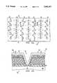
- FIG. 1ais a schematic representation showing a plan view with portions broken away of an infrared detector and its associated focal plane array and silicon processor at an intermediate stage in the fabrication process;
- FIG. 1bis a drawing in section with portions broken away taken along lines 1b--1b of FIG. 1a;
- FIG. 2ais a schematic representation showing a plan view with portions broken away of the infrared detector of FIG. 1a after the focal plane array has been covered with a layer of interconnect metal;
- FIG. 2bis a drawing in section with portions broken away taken along lines 2b--2b of FIG. 2a;
- FIG. 3ais a schematic representation showing a plan view with portions broken away of the infrared detector of FIG. 2a after selected portions of the metal interconnect layer have been covered with a photoresist;
- FIG. 3bis a drawing in section with portions broken away taken along lines 3b--3b of FIG. 3a;
- FIG. 4ais a schematic representation showing a plan view with portions broken away of the infrared detector of FIG. 3a after dry etching to form the desired metal interconnects or vias between thermal sensors in the focal plane array and contact pads on the silicon processor;
- FIG. 4bis a drawing in section with portions broken away taken along lines 4b--4b of FIG. 4a;
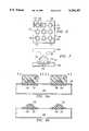
- FIG. 5is a schematic drawing in elevation and in section with portions broken away showing an RF chamber satisfactory for dry etching the infrared detector and focal plan array structure shown in FIGS. 3a and 3b;
- FIG. 6is a schematic representation showing a plan view with portions broken away of a substrate having a metal interconnect pattern formed in accordance with the present invention
- FIG. 7is a schematic representation with portions broken away taken along lines 7--7 of FIG. 6;
- FIG. 8ais a schematic representation in section with portions broken away showing a substrate at an intermediate stage in the fabrication process covered with a layer of interconnect metal and selected portions of the metal interconnect layer covered with a photoresist;
- FIG. 8bis a schematic drawing in section with portions broken away showing the substrate of FIG. 8a with a metal interconnect pattern formed using dry etching techniques in accordance with the present invention.
- FIGS. 1a through 8b of the drawingslike numerals being used for like and corresponding parts of the various drawings.
- Infrared detectors or thermal imaging systemsare typically based upon either the generation of a change in voltage due to a change in temperature resulting from incident infrared radiation striking a thermal sensor, or the generation of a change in voltage due to a photoelectron interaction within the material used to form the thermal sensor. This latter effect is sometimes called the internal photoelectric effect.
- the present inventionmay also be used to form metal interconnects associated with uncooled infrared detectors.
- detectorsare typically formed with a plurality of thermal sensors (not shown) having ferroelectric elements which generate a change in voltage due to a change in temperature of the ferroelectric material resulting from incident infrared radiation.
- thermal sensorsmay be formed from barium strontium titanate or other suitable ferroelectric materials.
- the present inventionallows fabricating a metal interconnect pattern for use in bump bonding ferroelectric thermal sensors with an integrated circuit substrate.
- Infrared detector or thermal imaging system 50may be manufactured from semiconductor materials which are structured as photodiodes and/or photocapacitors.
- U.S. Pat. No. 4,447,291 entitled Methods for Via Formation in HgCdTe, and U.S. Pat. No. 5,144,138 entitled Infrared Detector and Methodprovide information concerning infrared detectors fabricated from HgCdTe semiconductor materials and alloys which produce electron-hole pairs in response to incident infrared radiation.
- U.S. Pat. Nos. 4,447,291 and 5,144,138are incorporated by reference for all purposes in this application.
- FIGS. 1a through 4bare schematic representations of selected steps in the fabrication of infrared detector or thermal imaging system 50.
- Some of the principal components of thermal imaging system 50include focal plane array 60 and integrated circuit substrate or silicon processor 80.
- focal plane array 60comprises a plurality of individual thermal sensors or infrared detector elements 20.
- Each infrared detector element 20may be formed from several various types of material including semiconductor material such as HgCdTe which interacts with incident infrared radiation to produce electron-hole pairs.
- the various materials used to fabricate infrared detector elements 20are typically deposited in a series of layers on a suitable substrate using lithographic techniques.
- FIGS. 1b, 2b, 3b and 4bfor thermal imaging system 50, all infrared detector elements 20 are generally identical.
- Each infrared detector element 20is preferably disposed on planar surface 82 of silicon processor 80 adjacent to a corresponding contact pad 84.
- Via 62is preferably provided between adjacent thermal sensors 20 to allow access to the associated contact pad 84.
- via 62 shown in FIG. 1b between thermal sensors 20a and 20ballows forming a sensor signal flow path between storage gate 22 of thermal sensor 20b and the associated contact pad 84.
- Silicon processor 80is used to produce a thermal image based on incident infrared radiation striking infrared detector elements 20 in focal plane array 60.
- Infrared detector 50will preferably include a plurality (N ⁇ M) of infrared detector elements 20 forming focal plane array 60 bonded to silicon processor 80. Each infrared detector element 20 corresponds to a picture element or pixel in the resulting infrared image produced by infrared detector 50.
- focal plane array 60includes a plurality of storage gates 22 which correspond respectively with infrared detector elements 20.
- Each storage gate 22is preferable formed from metal such as nickel or tantalum which is relatively transparent to incident infrared radiation. Also, each storage gate 22 is preferably a thin strip of metal (often less than 100 angstroms thick) to further promote transparency with respect to incident infrared radiation.
- Each storage gate 22 and its associated infrared detector element 20are separated from adjacent infrared detector elements 20 with no electrical contact therebetween.
- each infrared detector element 20comprises a plurality of layers of different materials which are disposed on planar surface 82 of silicon processor 80.
- Each infrared detector element 20includes bar 24 of semiconductor material such as HgCdTe, which is sensitive to incident infrared radiation.
- HgCdTesemiconductor material
- the values of xmay be varied depending upon the desired sensitivity of the resulting thermal sensor 20 to different wavelengths of incident infrared radiation.
- Each bar 24may be mounted on surface 82 of silicon processor 80 using a suitable epoxy or other gluing compound.
- FIGS. 1b, 2b, 3b, and 4bthe respective bars 24 are shown attached to silicon processor 80 with epoxy layer 26.
- Silicon Processor 80typically represents one or more chips fabricated on the surface of a semi-conductor wafer such as semi-conductor wafers 86 shown in FIG. 5.
- a plurality of bars 24may be mounted on one or more chips to form a plurality of infrared detectors 50 on each semi-conductor wafer 86.
- Vias 62are formed between adjacent bars 24 corresponding with the location of each contact pad 84.
- U.S. Pat. 4,447,291discloses one process for mounting bars 24 and forming vias 62.
- An insulating layer 28 of zinc sulphide (ZnS)is preferably disposed on each bar 24 to protect semiconductor material HgCdTe and to position each storage gate 22 with respect to its associated bar 24.
- Each via 62includes an opening through insulating layer 28 and epoxy layer 26 to allow access to the associated contact pad 84. Applying insulating layer 28 also assists with maintaining the cleanliness of the exposed surfaces of focal plane array 60.
- the resulting intermediate structure formed during fabrication of infrared detector 50is shown in FIGS. 1a and 1b.
- the following steps in the fabrication processare directed towards forming a metal interconnect pattern to provide a plurality of sensor signal flow paths from each storage gate 22 through its associated via 62 to the respective contact pad 84 on silicon processor 80.
- the resulting metal interconnects 34may sometimes be referred to as "via interconnects,” “metal connectors,” or “metal strip conductors.”
- Metal film layer 30may be formed using sputter deposition techniques or other techniques appropriate for the material selected for layer 30.
- Prior fabrication processesoften involved placing a layer of photoresist covering the focal plane array prior to forming the desired metal interconnect between each thermal sensor and its associated contact pad.
- Forming metal film layer 30 on focal plane array 60 prior to applying any photoresist materialreduces potential surface contamination, increases the integrity of the metal bond with the respective storage gates 22 and contact pads 84.
- the number of electrical shorts resulting from incomplete bondingis substantially reduced by the use of metal film layer 30.
- the present inventionallows selecting various metals and metal alloys to form metal film layer 30.
- the metal film layerswhich may be satisfactorily used with the present invention include indium (In), indium/lead/indium (In/Pb/In), aluminum (Al), or aluminum/titanium-tungsten (Al/TiW).
- the present inventionmay also be used to form interconnect patterns from refractory metals such as titanium, tungsten, titanium-tungsten alloys, tantalum, molybdenum and alloys such as titanium silicon (Ti 4 Si 3 ) and titanium nitride (TIN).
- film layer 30is preferably formed from indium. This intermediate structure associated with the fabrication of infrared detector elements 20 is shown in FIGS. 2a and 2b.
- the next step in the processis to pattern a layer of photoresist material 32 at selected locations on metal film layer 30 as shown in FIGS. 3a and 3b.
- the position of each photoresist layer 32is selected to correspond with the desired location of each sensor signal flow path or metal strip conductor 34 between its associated storage gate 22 and contact pad 84.
- the following stepis dry etching to remove the portions of metal layer 30 which are not protected by photoresist layers 32. Following the dry etch, photoresist layers 32 are stripped away to leave metal strip conductors 34 as shown in FIGS. 4a and 4b. Ashing or solvent stripping may be used as desired to remove photoresist layers 32.
- Metal strip conductors 34are thus formed to extend from each storage gate 22 to the associated contact pad 84 and provide the desired sensor signal flow path.
- the dry etching process used to form metal strip conductors 34 from metal film layer 30may be conducted in various types of reactors.
- An RF discharge parallel plate reactor 90 satisfactory for use with the present inventionis shown in FIG. 5.
- One of the advantages of dry etchingis that the process may be performed at a relatively low temperature (less than 100° C.) as compared to other methods of forming metal connectors.
- Reactor 90includes housing 92 which contains chamber 94.
- Inlet 96is provided to supply gas from a source (not shown) to chamber 94.
- Outlet 98is provided to connect chamber 94 with a pump or other means (not shown) to form a vacuum within chamber 94.
- a pair of parallel electrodes 100 and 102are disposed in chamber 94.
- RF power used to facilitate the dry etching processis supplied to upper electrode 100.
- Wafers 86 having a plurality of silicon processors 80 and associated infrared detectors 50 formed on the surface of each wafer 86are preferably placed on lower or ground electrode 102.
- etching gasmay be satisfactorily used with the present invention.
- the selection of etching gasis dependent upon the metal or metal alloy used to form film layer 30.
- a hydrogen plasma with either an argon or helium carrierhas been particularly effective in the removal of indium metal by forming indium hydride.
- the hydrogen plasma etchmay be performed at temperatures less than 100° C.
- a hydrogen plasma etchmay be satisfactorily used for other metals and metal alloys.
- the relatively low temperature (less than 100° C.) required for hydrogen plasma etching in accordance with the present inventionis particularly beneficial for forming metal interconnect patterns from soft alloys and low melting temperature alloys.
- various methyl alkyl groupsmay be used as part of the dry etching process depending upon the type of metal or alloys used to form the film layer.
- Semiconductor wafers 86 on ground electrode 102are subjected to the selected etch plasma or gas which reacts with the unprotected portion of metal film layer 30.
- the resulting metal hydrides or organometallic productsare removed from chamber 84 through outlet 98.
- the type of organometallic product formed by the etching processdepends upon the constituents in the metal film layer 30 and the plasma etch gas.
- metal film layer 30is formed from indium.
- hydrogen radicalsformed with the aid of the RF energy, will combine with indium metal which has not been covered by photoresist layers 32 to form indium hydrides.
- the indium hydridesbecome volatile and are removed from the surface of focal plane array 60.
- Photoresist layers 32protect the portions of metal film layer 30 which will become metal strip conducts 34 following the dry etching process. The result is a plurality of strips of indium 34 extending from each storage gate 22 to the corresponding pad 84.
- Metal layer 30may be formed from indium and various indium alloys including lead indium.
- the present inventionmay be used to form various types of metal interconnect patterns in addition to metal strip conductors 34 shown in FIG. 4a.
- some hybrid solid state systemsare formed by bump bonding component structures having corresponding bumps of indium metal.
- substrate 110includes a plurality of indium bumps 112 formed on planar surface 114.
- Each indium bump 112is preferably disposed on an associated contact pad 116 with barrier layer 118 therebetween.
- Barrier layer 118may be formed from various metals and alloys such as nickel, chrome or titanium-tungsten.
- the material used to form barrier 118is preferably selected to provide mechanical bonding and electrical contact between indium bump 112 and the associated contact pad 116 while at the same time minimizing potential corrosion between indium bump 112 and contact pad 116.
- substrate 120 with indium bump 122may be bonded with corresponding indium bump 112 on substrate 110.
- Indium bumps 112 and 122may be formed on their respective substrates 110 and 120 by forming a layer of indium metal on the surface of each substrate and dry etching the indium metal layer in accordance with the present invention.
- thermal isolation structures and bump bondsare shown in U.S. Pat. No. 5,047,644 entitled Polyamide Thermal Isolation Mesa for a Thermal Imaging System to Meissner, et al.
- the fabrication techniques and the materials used in U.S. Pat. No. 5,047,644may be used in fabricating either substrate 110 or 120.
- U.S. Pat. No. 5,047,644is incorporated by reference for all purposes in this patent application.
- U.S. Pat. No. 4,143,269 entitled Ferroelectric Imaging Systemprovides information concerning infrared detectors fabricated from ferroelectric materials and a silicon switching matrix or integrated circuit substrate.
- Substrate 120may be formed with a plurality of ferroelectric thermal sensors and substrate 110 may comprise an integrated circuit substrate as shown in U.S. Pat. No. 4,143,269.
- U.S. Pat. No. 4,143,269is incorporated by reference for all purposes in this patent application.
- FIGS. 8a and 8bare schematic representations showing the fabrication of metal interconnects 132 on the surface of integrated circuit substrate 130 using the present invention.
- Integrated circuit substrate 130preferably includes a plurality of contact pads 134 with polyamide bumps 136 formed on the surface of each contact pad 134.
- the configuration of polyamide bumps 136may be selected to correspond with the desired metal interconnect pattern.
- a layer of interconnect metal 138may be disposed over the surface of substrate 130 including polyamide bumps 136. Layers 140 of appropriate photoresist material are next placed on metal layer 138 to correspond with the desired metal interconnect pattern. Substrate 130 may then be placed in RF chamber 90 and dry etched in accordance with the present invention to form a plurality of metal interconnects 132 on the surface of substrate 130.
- metal film layer 138is preferably formed from indium or alloys of indium. The resulting metal interconnects 132 may be used to bump bond a focal plane array with an integrated circuit substrate.
- the present inventionallows forming metal bumps, solder patterns, metal strips, or any other geometric configuration as desired from a layer of metal film.
- the requirements for forming a metal interconnect pattern in accordance with the present inventionare positioning a photoresist on a metal film layer to produce the desired configuration and selecting a dry etch gas which will react with the unprotected portions of the metal film layer.
Landscapes
- Physics & Mathematics (AREA)
- Condensed Matter Physics & Semiconductors (AREA)
- General Physics & Mathematics (AREA)
- Engineering & Computer Science (AREA)
- Computer Hardware Design (AREA)
- Microelectronics & Electronic Packaging (AREA)
- Power Engineering (AREA)
- Photometry And Measurement Of Optical Pulse Characteristics (AREA)
Abstract
Description
Claims (29)
Priority Applications (1)
| Application Number | Priority Date | Filing Date | Title |
|---|---|---|---|
| US08/140,390US5384267A (en) | 1993-10-19 | 1993-10-19 | Method of forming infrared detector by hydrogen plasma etching to form refractory metal interconnects |
Applications Claiming Priority (1)
| Application Number | Priority Date | Filing Date | Title |
|---|---|---|---|
| US08/140,390US5384267A (en) | 1993-10-19 | 1993-10-19 | Method of forming infrared detector by hydrogen plasma etching to form refractory metal interconnects |
Publications (1)
| Publication Number | Publication Date |
|---|---|
| US5384267Atrue US5384267A (en) | 1995-01-24 |
Family
ID=22491023
Family Applications (1)
| Application Number | Title | Priority Date | Filing Date |
|---|---|---|---|
| US08/140,390Expired - LifetimeUS5384267A (en) | 1993-10-19 | 1993-10-19 | Method of forming infrared detector by hydrogen plasma etching to form refractory metal interconnects |
Country Status (1)
| Country | Link |
|---|---|
| US (1) | US5384267A (en) |
Cited By (12)
| Publication number | Priority date | Publication date | Assignee | Title |
|---|---|---|---|---|
| US5552326A (en)* | 1995-03-01 | 1996-09-03 | Texas Instruments Incorporated | Method for forming electrical contact to the optical coating of an infrared detector using conductive epoxy |
| US5589404A (en)* | 1994-08-01 | 1996-12-31 | Lucent Technologies Inc. | Monolithically integrated VLSI optoelectronic circuits and a method of fabricating the same |
| US5652150A (en)* | 1995-06-07 | 1997-07-29 | Texas Instruments Incorporated | Hybrid CCD imaging |
| US6025269A (en)* | 1996-10-15 | 2000-02-15 | Micron Technology, Inc. | Method for depositioning a substantially void-free aluminum film over a refractory metal nitride layer |
| US6146964A (en)* | 1997-06-13 | 2000-11-14 | Oki Electric Industry Co., Ltd. | Method of manufacturing a semiconductor device having a fin type capacitor electrode |
| US20020175331A1 (en)* | 2001-05-22 | 2002-11-28 | Shinji Isokawa | Structure and method for mounting a semiconductor element |
| US20020190839A1 (en)* | 1998-12-07 | 2002-12-19 | Aravind Padmanabhan | Integratable fluid flow and property microsensor assembly |
| US6576490B2 (en)* | 2001-05-09 | 2003-06-10 | National Research Council Of Canada | Method for micro-fabricating a pixelless infrared imaging device |
| US6853083B1 (en)* | 1995-03-24 | 2005-02-08 | Semiconductor Energy Laboratory Co., Ltd. | Thin film transfer, organic electroluminescence display device and manufacturing method of the same |
| US6972746B1 (en) | 1994-10-31 | 2005-12-06 | Semiconductor Energy Laboratory Co., Ltd. | Active matrix type flat-panel display device |
| US8679359B2 (en)* | 2010-05-10 | 2014-03-25 | Georgia Tech Research Corporation | Low temperature metal etching and patterning |
| US12317757B2 (en) | 2018-10-11 | 2025-05-27 | SeeQC, Inc. | System and method for superconducting multi-chip module |
Citations (20)
| Publication number | Priority date | Publication date | Assignee | Title |
|---|---|---|---|---|
| US3962578A (en)* | 1975-02-28 | 1976-06-08 | Aeronutronic Ford Corporation | Two-color photoelectric detectors having an integral filter |
| US4085500A (en)* | 1975-07-17 | 1978-04-25 | Honeywell Inc. | Ohmic contacts to p-type mercury cadmium telluride |
| US4143269A (en)* | 1977-12-19 | 1979-03-06 | Texas Instruments Incorporated | Ferroelectric imaging system |
| EP0090669A2 (en)* | 1982-03-31 | 1983-10-05 | Honeywell Inc. | Electromagnetic radiation detector |
| US4412732A (en)* | 1980-07-21 | 1983-11-01 | Ricoh Company, Ltd. | Transfer medium separating device |
| US4447291A (en)* | 1983-08-31 | 1984-05-08 | Texas Instruments Incorporated | Method for via formation in HgCdTe |
| US4614957A (en)* | 1982-03-31 | 1986-09-30 | Honeywell Inc. | Electromagnetic radiation detectors |
| US4639756A (en)* | 1986-05-05 | 1987-01-27 | Santa Barbara Research Center | Graded gap inversion layer photodiode array |
| US4663529A (en)* | 1984-08-24 | 1987-05-05 | U.S. Philips Corporation | Thermal imaging device and a method of manufacturing a thermal imaging device |
| US4684812A (en)* | 1983-08-31 | 1987-08-04 | Texas Instruments Incorporated | Switching circuit for a detector array |
| US4948976A (en)* | 1989-02-09 | 1990-08-14 | Servo Corporation Of America | Multi-wavelength band infrared detector |
| US4965649A (en)* | 1988-12-23 | 1990-10-23 | Ford Aerospace Corporation | Manufacture of monolithic infrared focal plane arrays |
| US5047644A (en)* | 1989-07-31 | 1991-09-10 | Texas Instruments Incorporated | Polyimide thermal isolation mesa for a thermal imaging system |
| US5113076A (en)* | 1989-12-19 | 1992-05-12 | Santa Barbara Research Center | Two terminal multi-band infrared radiation detector |
| US5144138A (en)* | 1989-10-06 | 1992-09-01 | Texas Instruments Incorporated | Infrared detector and method |
| US5188970A (en)* | 1989-06-29 | 1993-02-23 | Texas Instruments Incorporated | Method for forming an infrared detector having a refractory metal |
| US5236871A (en)* | 1992-04-29 | 1993-08-17 | The United States Of America As Represented By The Administrator Of The National Aeronautics And Space Administration | Method for producing a hybridization of detector array and integrated circuit for readout |
| US5246875A (en)* | 1991-10-15 | 1993-09-21 | Goldstar Electron Co., Ltd. | Method of making charge coupled device image sensor |
| US5273910A (en)* | 1990-08-08 | 1993-12-28 | Minnesota Mining And Manufacturing Company | Method of making a solid state electromagnetic radiation detector |
| US5318666A (en)* | 1993-04-19 | 1994-06-07 | Texas Instruments Incorporated | Method for via formation and type conversion in group II and group VI materials |
- 1993
- 1993-10-19USUS08/140,390patent/US5384267A/ennot_activeExpired - Lifetime
Patent Citations (20)
| Publication number | Priority date | Publication date | Assignee | Title |
|---|---|---|---|---|
| US3962578A (en)* | 1975-02-28 | 1976-06-08 | Aeronutronic Ford Corporation | Two-color photoelectric detectors having an integral filter |
| US4085500A (en)* | 1975-07-17 | 1978-04-25 | Honeywell Inc. | Ohmic contacts to p-type mercury cadmium telluride |
| US4143269A (en)* | 1977-12-19 | 1979-03-06 | Texas Instruments Incorporated | Ferroelectric imaging system |
| US4412732A (en)* | 1980-07-21 | 1983-11-01 | Ricoh Company, Ltd. | Transfer medium separating device |
| EP0090669A2 (en)* | 1982-03-31 | 1983-10-05 | Honeywell Inc. | Electromagnetic radiation detector |
| US4614957A (en)* | 1982-03-31 | 1986-09-30 | Honeywell Inc. | Electromagnetic radiation detectors |
| US4447291A (en)* | 1983-08-31 | 1984-05-08 | Texas Instruments Incorporated | Method for via formation in HgCdTe |
| US4684812A (en)* | 1983-08-31 | 1987-08-04 | Texas Instruments Incorporated | Switching circuit for a detector array |
| US4663529A (en)* | 1984-08-24 | 1987-05-05 | U.S. Philips Corporation | Thermal imaging device and a method of manufacturing a thermal imaging device |
| US4639756A (en)* | 1986-05-05 | 1987-01-27 | Santa Barbara Research Center | Graded gap inversion layer photodiode array |
| US4965649A (en)* | 1988-12-23 | 1990-10-23 | Ford Aerospace Corporation | Manufacture of monolithic infrared focal plane arrays |
| US4948976A (en)* | 1989-02-09 | 1990-08-14 | Servo Corporation Of America | Multi-wavelength band infrared detector |
| US5188970A (en)* | 1989-06-29 | 1993-02-23 | Texas Instruments Incorporated | Method for forming an infrared detector having a refractory metal |
| US5047644A (en)* | 1989-07-31 | 1991-09-10 | Texas Instruments Incorporated | Polyimide thermal isolation mesa for a thermal imaging system |
| US5144138A (en)* | 1989-10-06 | 1992-09-01 | Texas Instruments Incorporated | Infrared detector and method |
| US5113076A (en)* | 1989-12-19 | 1992-05-12 | Santa Barbara Research Center | Two terminal multi-band infrared radiation detector |
| US5273910A (en)* | 1990-08-08 | 1993-12-28 | Minnesota Mining And Manufacturing Company | Method of making a solid state electromagnetic radiation detector |
| US5246875A (en)* | 1991-10-15 | 1993-09-21 | Goldstar Electron Co., Ltd. | Method of making charge coupled device image sensor |
| US5236871A (en)* | 1992-04-29 | 1993-08-17 | The United States Of America As Represented By The Administrator Of The National Aeronautics And Space Administration | Method for producing a hybridization of detector array and integrated circuit for readout |
| US5318666A (en)* | 1993-04-19 | 1994-06-07 | Texas Instruments Incorporated | Method for via formation and type conversion in group II and group VI materials |
Non-Patent Citations (8)
| Title |
|---|
| E. R. Blazejewski, et al., "Bias-Switchable Dual-Band HgCdTe Infrared Photodetector," J. Vac. Sci. Technol. B 10(4), Jul./Aug. 1992, 1992 American Vacuum Society, pp. 1626-1632. |
| E. R. Blazejewski, et al., "Bias-Switchable Dual-Band HgCdTe IR Photodetector", Presented at the IRIS Detectors Specialty Meeting in Boulder, Colo., Aug. 1991. |
| E. R. Blazejewski, et al., Bias Switchable Dual Band HgCdTe Infrared Photodetector, J. Vac. Sci. Technol. B 10(4), Jul./Aug. 1992, 1992 American Vacuum Society, pp. 1626 1632.* |
| E. R. Blazejewski, et al., Bias Switchable Dual Band HgCdTe IR Photodetector , Presented at the IRIS Detectors Specialty Meeting in Boulder, Colo., Aug. 1991.* |
| M. W. Goddwin, et al., "Metal-Insulator Semiconductor Properties of Molecular-Beam Epitaxy Grown HgCdTe Heterostructures," J. Vac. Sci. Technol. vol. 8, No. 2, Mar./Apr. 1990, pp. 1226-1232. |
| M. W. Goddwin, et al., Metal Insulator Semiconductor Properties of Molecular Beam Epitaxy Grown HgCdTe Heterostructures, J. Vac. Sci. Technol. vol. 8, No. 2, Mar./Apr. 1990, pp. 1226 1232.* |
| T. N. Casselman, et al., "An Integrated Multispectral IR Detector Structure", pp. 141-142, 1991. |
| T. N. Casselman, et al., An Integrated Multispectral IR Detector Structure , pp. 141 142, 1991.* |
Cited By (22)
| Publication number | Priority date | Publication date | Assignee | Title |
|---|---|---|---|---|
| US5589404A (en)* | 1994-08-01 | 1996-12-31 | Lucent Technologies Inc. | Monolithically integrated VLSI optoelectronic circuits and a method of fabricating the same |
| US6972746B1 (en) | 1994-10-31 | 2005-12-06 | Semiconductor Energy Laboratory Co., Ltd. | Active matrix type flat-panel display device |
| US7298357B2 (en) | 1994-10-31 | 2007-11-20 | Semiconductor Energy Laboratory Co., Ltd. | Active matrix type flat-panel display device |
| US20060033690A1 (en)* | 1994-10-31 | 2006-02-16 | Semiconductor Energy Laboratory Co., Ltd. | Active matrix type flat-panel display device |
| US5552326A (en)* | 1995-03-01 | 1996-09-03 | Texas Instruments Incorporated | Method for forming electrical contact to the optical coating of an infrared detector using conductive epoxy |
| US6853083B1 (en)* | 1995-03-24 | 2005-02-08 | Semiconductor Energy Laboratory Co., Ltd. | Thin film transfer, organic electroluminescence display device and manufacturing method of the same |
| US6992435B2 (en) | 1995-03-24 | 2006-01-31 | Semiconductor Energy Laboratory Co., Ltd. | Thin film transistor, organic electroluminescence display device and manufacturing method of the same |
| US7476900B2 (en) | 1995-03-24 | 2009-01-13 | Semiconductor Energy Laboratory Co., Ltd. | Thin film transistor, organic electroluminescence display device and manufacturing method of the same |
| US20050146262A1 (en)* | 1995-03-24 | 2005-07-07 | Semiconductor Energy Laboratory Co., Ltd. | Thin film transistor, organic electroluminescence display device and manufacturing method of the same |
| US20060087222A1 (en)* | 1995-03-24 | 2006-04-27 | Semiconductor Energy Laboratory Co., Ltd. | Thin film transistor, organic electroluminescence display device and manufacturing method of the same |
| US5652150A (en)* | 1995-06-07 | 1997-07-29 | Texas Instruments Incorporated | Hybrid CCD imaging |
| US6025269A (en)* | 1996-10-15 | 2000-02-15 | Micron Technology, Inc. | Method for depositioning a substantially void-free aluminum film over a refractory metal nitride layer |
| US6146964A (en)* | 1997-06-13 | 2000-11-14 | Oki Electric Industry Co., Ltd. | Method of manufacturing a semiconductor device having a fin type capacitor electrode |
| US6794981B2 (en)* | 1998-12-07 | 2004-09-21 | Honeywell International Inc. | Integratable-fluid flow and property microsensor assembly |
| US20020190839A1 (en)* | 1998-12-07 | 2002-12-19 | Aravind Padmanabhan | Integratable fluid flow and property microsensor assembly |
| US6750072B2 (en)* | 2001-05-09 | 2004-06-15 | National Research Council Of Canada | Method for micro-fabricating a pixelless infrared imaging device |
| US20030211648A1 (en)* | 2001-05-09 | 2003-11-13 | Margaret Buchanan | Method for micro-fabricating a pixelles infrared imaging device |
| US6576490B2 (en)* | 2001-05-09 | 2003-06-10 | National Research Council Of Canada | Method for micro-fabricating a pixelless infrared imaging device |
| US6686607B2 (en)* | 2001-05-22 | 2004-02-03 | Rohm Co., Ltd. | Structure and method for mounting a semiconductor element |
| US20020175331A1 (en)* | 2001-05-22 | 2002-11-28 | Shinji Isokawa | Structure and method for mounting a semiconductor element |
| US8679359B2 (en)* | 2010-05-10 | 2014-03-25 | Georgia Tech Research Corporation | Low temperature metal etching and patterning |
| US12317757B2 (en) | 2018-10-11 | 2025-05-27 | SeeQC, Inc. | System and method for superconducting multi-chip module |
Similar Documents
| Publication | Publication Date | Title |
|---|---|---|
| US5525527A (en) | Process for producing a solid state radiation detector | |
| EP0864171B1 (en) | Forming contacts on semiconductor substrates for radiation detectors and imaging devices | |
| US5743006A (en) | Method for fabricating a focal plane array for thermal imaging system | |
| US5384267A (en) | Method of forming infrared detector by hydrogen plasma etching to form refractory metal interconnects | |
| US4197633A (en) | Hybrid mosaic IR/CCD focal plane | |
| US4286278A (en) | Hybrid mosaic IR/CCD focal plane | |
| EP0677500B1 (en) | Multiple level mask for patterning of ceramic materials | |
| US5064771A (en) | Method of forming crystal array | |
| US4206470A (en) | Thin film interconnect for multicolor IR/CCD | |
| US4196508A (en) | Durable insulating protective layer for hybrid CCD/mosaic IR detector array | |
| US5959298A (en) | Infrared detector array with an elevated thin film | |
| EP0663696B1 (en) | Thermal imaging device | |
| US5646066A (en) | Method for forming electrical contact to the optical coating of an infrared detector from the backside of the detector | |
| US4275407A (en) | Durable insulating protective layer for hybrid CCD/mosaic IR detector array | |
| CN100438080C (en) | Radiation detector with one or more conductive contacts and method of making same | |
| WO1994017557A1 (en) | Thermally matched readout/detector assembly and method for fabricating same | |
| US6080987A (en) | Infrared-sensitive conductive-polymer coating | |
| US5631467A (en) | Etching of ceramic materials with an elevated thin film | |
| US5466331A (en) | Elevated thin film for ceramic materials | |
| US4137625A (en) | Thin film interconnect for multicolor IR/CCD | |
| EP0037244B1 (en) | Method for fabricating a solid-state imaging device using photoconductive film | |
| Sánchez et al. | Progress on monolithic integration of cheap IR FPAs of polycrystalline PbSe | |
| JP2978211B2 (en) | Apparatus for infrared detector with refractory metal | |
| KR100290442B1 (en) | Thermal Image Semiconductor Device | |
| HK1010282B (en) | Forming contacts on semiconductor substrates for radiation detectors and imaging devices |
Legal Events
| Date | Code | Title | Description |
|---|---|---|---|
| AS | Assignment | Owner name:TEXAS INSTRUMENTS INCORPORATED, TEXAS Free format text:ASSIGNMENT OF ASSIGNORS INTEREST;ASSIGNOR:HUTCHINS, LARRY D.;REEL/FRAME:006755/0139 Effective date:19931018 | |
| STCF | Information on status: patent grant | Free format text:PATENTED CASE | |
| FPAY | Fee payment | Year of fee payment:4 | |
| AS | Assignment | Owner name:RAYTHEON COMPANY, MASSACHUSETTS Free format text:ASSIGNMENT OF ASSIGNORS INTEREST;ASSIGNOR:TEXAS INSTRUMENTS INCORPORATED;REEL/FRAME:009764/0360 Effective date:19990212 | |
| FEPP | Fee payment procedure | Free format text:PAYOR NUMBER ASSIGNED (ORIGINAL EVENT CODE: ASPN); ENTITY STATUS OF PATENT OWNER: LARGE ENTITY | |
| FPAY | Fee payment | Year of fee payment:8 | |
| FPAY | Fee payment | Year of fee payment:12 | |
| AS | Assignment | Owner name:OL SECURITY LIMITED LIABILITY COMPANY, DELAWARE Free format text:ASSIGNMENT OF ASSIGNORS INTEREST;ASSIGNOR:RAYTHEON COMPANY;REEL/FRAME:029117/0335 Effective date:20120730 | |
| FEPP | Fee payment procedure | Free format text:PAYER NUMBER DE-ASSIGNED (ORIGINAL EVENT CODE: RMPN); ENTITY STATUS OF PATENT OWNER: LARGE ENTITY Free format text:PAYOR NUMBER ASSIGNED (ORIGINAL EVENT CODE: ASPN); ENTITY STATUS OF PATENT OWNER: LARGE ENTITY | |
| AS | Assignment | Owner name:TEXAS INSTRUMENTS INCORPORATED, TEXAS Free format text:ASSIGNMENT OF ASSIGNORS INTEREST;ASSIGNORS:HUTCHINS, LARRY D.;YORK, RUDY L.;REEL/FRAME:030239/0099 Effective date:19931018 |