US5382770A - Mirror-based laser-processing system with visual tracking and position control of a moving laser spot - Google Patents
Mirror-based laser-processing system with visual tracking and position control of a moving laser spotDownload PDFInfo
- Publication number
- US5382770A US5382770AUS08/004,709US470993AUS5382770AUS 5382770 AUS5382770 AUS 5382770AUS 470993 AUS470993 AUS 470993AUS 5382770 AUS5382770 AUS 5382770A
- Authority
- US
- United States
- Prior art keywords
- laser
- mirror
- laser beam
- beam splitter
- infrared
- Prior art date
- Legal status (The legal status is an assumption and is not a legal conclusion. Google has not performed a legal analysis and makes no representation as to the accuracy of the status listed.)
- Expired - Lifetime
Links
- 238000012545processingMethods0.000titleclaimsabstractdescription31
- 230000000007visual effectEffects0.000titleclaimsdescription10
- 238000003466weldingMethods0.000claimsabstractdescription44
- 239000011248coating agentSubstances0.000claimsabstractdescription7
- 238000000576coating methodMethods0.000claimsabstractdescription7
- 238000003384imaging methodMethods0.000claimsdescription5
- 238000001208nuclear magnetic resonance pulse sequenceMethods0.000claimsdescription5
- 238000010168coupling processMethods0.000claimsdescription3
- 238000005859coupling reactionMethods0.000claimsdescription3
- 238000011282treatmentMethods0.000description12
- 238000000034methodMethods0.000description9
- 238000009826distributionMethods0.000description8
- 238000004519manufacturing processMethods0.000description5
- 239000000463materialSubstances0.000description5
- 230000008569processEffects0.000description5
- 238000005520cutting processMethods0.000description4
- 230000003287optical effectEffects0.000description4
- 238000010276constructionMethods0.000description2
- 230000001788irregularEffects0.000description2
- 238000013532laser treatmentMethods0.000description2
- 230000007246mechanismEffects0.000description2
- 238000012544monitoring processMethods0.000description2
- 239000004033plasticSubstances0.000description2
- 229920003023plasticPolymers0.000description2
- 230000004044responseEffects0.000description2
- 238000001228spectrumMethods0.000description2
- 235000011449RosaNutrition0.000description1
- 230000004075alterationEffects0.000description1
- 238000010923batch productionMethods0.000description1
- 230000015572biosynthetic processEffects0.000description1
- 230000008859changeEffects0.000description1
- 230000001427coherent effectEffects0.000description1
- 230000006378damageEffects0.000description1
- 238000013461designMethods0.000description1
- 238000001914filtrationMethods0.000description1
- 229910052751metalInorganic materials0.000description1
- 239000002184metalSubstances0.000description1
- 150000002739metalsChemical class0.000description1
- 238000012986modificationMethods0.000description1
- 230000004048modificationEffects0.000description1
- 230000035515penetrationEffects0.000description1
- 238000002310reflectometryMethods0.000description1
- 239000004065semiconductorSubstances0.000description1
- 230000003685thermal hair damageEffects0.000description1
- 238000010871transoral laser microsurgeryMethods0.000description1
Images

Classifications
- B—PERFORMING OPERATIONS; TRANSPORTING
- B23—MACHINE TOOLS; METAL-WORKING NOT OTHERWISE PROVIDED FOR
- B23K—SOLDERING OR UNSOLDERING; WELDING; CLADDING OR PLATING BY SOLDERING OR WELDING; CUTTING BY APPLYING HEAT LOCALLY, e.g. FLAME CUTTING; WORKING BY LASER BEAM
- B23K26/00—Working by laser beam, e.g. welding, cutting or boring
- B23K26/02—Positioning or observing the workpiece, e.g. with respect to the point of impact; Aligning, aiming or focusing the laser beam
- B23K26/03—Observing, e.g. monitoring, the workpiece
- B23K26/032—Observing, e.g. monitoring, the workpiece using optical means
- B—PERFORMING OPERATIONS; TRANSPORTING
- B23—MACHINE TOOLS; METAL-WORKING NOT OTHERWISE PROVIDED FOR
- B23K—SOLDERING OR UNSOLDERING; WELDING; CLADDING OR PLATING BY SOLDERING OR WELDING; CUTTING BY APPLYING HEAT LOCALLY, e.g. FLAME CUTTING; WORKING BY LASER BEAM
- B23K26/00—Working by laser beam, e.g. welding, cutting or boring
- B23K26/02—Positioning or observing the workpiece, e.g. with respect to the point of impact; Aligning, aiming or focusing the laser beam
- B23K26/04—Automatically aligning, aiming or focusing the laser beam, e.g. using the back-scattered light
- B—PERFORMING OPERATIONS; TRANSPORTING
- B23—MACHINE TOOLS; METAL-WORKING NOT OTHERWISE PROVIDED FOR
- B23K—SOLDERING OR UNSOLDERING; WELDING; CLADDING OR PLATING BY SOLDERING OR WELDING; CUTTING BY APPLYING HEAT LOCALLY, e.g. FLAME CUTTING; WORKING BY LASER BEAM
- B23K26/00—Working by laser beam, e.g. welding, cutting or boring
- B23K26/02—Positioning or observing the workpiece, e.g. with respect to the point of impact; Aligning, aiming or focusing the laser beam
- B23K26/06—Shaping the laser beam, e.g. by masks or multi-focusing
- B23K26/064—Shaping the laser beam, e.g. by masks or multi-focusing by means of optical elements, e.g. lenses, mirrors or prisms
- B23K26/0643—Shaping the laser beam, e.g. by masks or multi-focusing by means of optical elements, e.g. lenses, mirrors or prisms comprising mirrors
- B—PERFORMING OPERATIONS; TRANSPORTING
- B23—MACHINE TOOLS; METAL-WORKING NOT OTHERWISE PROVIDED FOR
- B23K—SOLDERING OR UNSOLDERING; WELDING; CLADDING OR PLATING BY SOLDERING OR WELDING; CUTTING BY APPLYING HEAT LOCALLY, e.g. FLAME CUTTING; WORKING BY LASER BEAM
- B23K26/00—Working by laser beam, e.g. welding, cutting or boring
- B23K26/02—Positioning or observing the workpiece, e.g. with respect to the point of impact; Aligning, aiming or focusing the laser beam
- B23K26/06—Shaping the laser beam, e.g. by masks or multi-focusing
- B23K26/0665—Shaping the laser beam, e.g. by masks or multi-focusing by beam condensation on the workpiece, e.g. for focusing
- B—PERFORMING OPERATIONS; TRANSPORTING
- B23—MACHINE TOOLS; METAL-WORKING NOT OTHERWISE PROVIDED FOR
- B23K—SOLDERING OR UNSOLDERING; WELDING; CLADDING OR PLATING BY SOLDERING OR WELDING; CUTTING BY APPLYING HEAT LOCALLY, e.g. FLAME CUTTING; WORKING BY LASER BEAM
- B23K26/00—Working by laser beam, e.g. welding, cutting or boring
- B23K26/02—Positioning or observing the workpiece, e.g. with respect to the point of impact; Aligning, aiming or focusing the laser beam
- B23K26/06—Shaping the laser beam, e.g. by masks or multi-focusing
- B23K26/067—Dividing the beam into multiple beams, e.g. multifocusing
Definitions
- the present inventionrelates to the field of laser processing, particularly to a mirror-based laser-processing system, e.g., a laser welding system, with visual tracking and position control of the moving welding spot.
- a mirror-based laser-processing systeme.g., a laser welding system
- the system described in the abovementioned patentis a lens-based optical system which is designed only for a predetermined wavelength of the transmitted light. Furthermore, such a system poorly transmits UV light, is very expensive, and cannot be used for low-energy applications, such as treating low-melting-point materials.
- U.S. Pat. No. 4,532,404describes a system which allows to carry out temperature control of the welding spot by means of a thermal sensor of a photo-electric type.
- a thermal sensor of a photo-electric typedoes not provide a thermal image of the treatment area and makes it impossible to obtain a thermal distribution pattern around the area of the welding spot. This is because the abovementioned sensor detects the integral thermal energy and does not differentiate between the points of the temperature pattern.
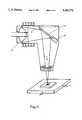
- FIG. 1is a general schematic view of the laser welding system of the invention with manual control from a joystick.
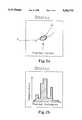
- FIG. 2Ais a thermal image and the position of a thermal cursor on the treatment path.
- FIG. 2Bis a thermal histogram across the treatment area.
- FIG. 3is an opto-mechanical schematic view of the laser welding system of the invention with X and Y table stage.
- a system of the present inventionis designed for treating, e.g., welding or cutting objects which have irregular patterns and are produced individually or in a very small batches, i.e., when programming is costly, time consuming, and not flexible.
- FIG. 1is a general schematic view of this system with manual control from a joystick and with parts of the system's elements represented three-dimensionally.
- the systemcontains a laser source 10 of any type suitable for laser welding.
- laser source 10of any type suitable for laser welding.
- examples of such sourcesare an Nd:YAG-type, eximer-type, and an CO 2 laser source which are produced by many companies, e.g., by Coherent, Inc., California.
- laser source 10On its output end, laser source 10 has a laser shutter 12 which controls the duration and the repetition rate of a laser beam B emitted from source 10. The operation of laser shutter 12 is controlled remotely through a feedback loop from the treatment area, which will be described later. Laser source 10 may generate a visible aiming beam (not shown) which is used for preliminarily aligning and focusing of the laser unit prior to the generation of the power beam.
- the next unit in the direction of propagation of laser beam B from source 10is a mirror-type laser micromanipulator 14 which is located between a laser source 10 and a wavelength-selective beam-splitter system 20.
- Mirror-type laser micromanipulator 14consists of a cylindrical housing 15 which holds two coaxially-arranged aspherical mirrors, i.e., a small-diameter convex mirror 16, a convex front surface 16a of which faces incident laser beam B emitted from source 10, and a large-diameter concave mirror 18 which has a central opening 17 for passing a laser beam toward mirror 16.
- Mirror 18has its concave front surface 18a facing convex front surface 16a of mirror 16.
- Micromanipulator 14has a zoom system 19 which may comprise an outer thread on the outer surface of housing 15 and an inner thread on the inner surface of a ring 19, so that by rotating ring 19 it is possible to change a focusing distance of micromanipulator 14 by changing the distance between mirrors 16 and 18 in response to the variation of the operation conditions, such as the different dimensions of an object O being treated, different magnification factors, different microscope heads, etc.
- a zoom system 19which may comprise an outer thread on the outer surface of housing 15 and an inner thread on the inner surface of a ring 19, so that by rotating ring 19 it is possible to change a focusing distance of micromanipulator 14 by changing the distance between mirrors 16 and 18 in response to the variation of the operation conditions, such as the different dimensions of an object O being treated, different magnification factors, different microscope heads, etc.
- the above-described mirror-based systemensures that the aiming beam and the processing beam are focused at the same point on object O with absolute accuracy. This results from the nature of the mirror system itself and cannot be achieved with the use of a lens system.
- Laser beam Breceived by mirror 16, is reflected in a diverging manner toward mirror 18, which, in turn reflects it in a converging manner towards a laser beam splitter 20.
- the lattercomprises a plain-parallel plate with a special wavelength-selective coating.
- This coatingpossesses a high reflectivity and a high damage threshold with respect to the working laser wavelength and therefore reflects the incident laser beam B toward the treatment area of object O.
- the same coatingis highly permeable to visible VL and infrared IL lights, which have wavelengths significantly different from those of the laser beam.
- laser beam Bwill be reflected onto the object for treating, e.g., welding the object, while image components (VL and IL) will be transmitted through beam splitter 20 for further use in the formation of a visible image and an infrared image.
- the reflected laser beam Bis focused at a point of treatment, e.g., at a welding spot W on the surface of object O.
- Beam splitters 20 of the type described abovecan be produced, e.g., by OCLI Corp., Santa Rosa, Calif.
- an imaging beam splitter 22Located on the side of beam splitter 20 opposite to object O is an imaging beam splitter 22 which also is made in the form of a plane-parallel plate having a special coating (not shown) which transmits visible light VL and reflects infrared light IL.
- a splitter of this typealso can be produced by OCLI Corp.
- Visible light VLis directed to a changeable microscope head 24 through a visible-light filter 26 which passes only visible components of the spectrum.
- Microscopic head 24can be focused onto object O and used for initial positioning of laser spot W on object O.
- Infrared light ILis directed through a sequence of optical elements which form an infrared tracking system with electron control and which are described below.
- the first element of this system in the direction of propagation of the infrared lightis an infrared filter 28 which passes the light corresponding only to the infrared part of the spectrum and also blocks the laser infrared wavelengths used for treating an object.
- Located behind filter 28is an infrared objective lens 30 which forms an infrared thermal image of object O.
- a chopper 32which is controlled by a driver 34 connected to one input of a lock-in amplifier 36.
- Chopper 32converts continuous infrared light into a discrete-pulse sequence which is then used, in a conventional manner, for subtracting the background infrared light, as is known in the art.
- Another input of the lock-in amplifieris connected to an output of a processing unit 38 which is built on the basis of conventional IC circuits and processes electrical-signal data into a visible image on a display.
- the second output of the processing unitis connected to the input of a laser controller 40 which is designed to stabilize the power supplied to laser source 10 and controls through a feedback loop FS the operation of laser shutter 12, in response to the changes in the temperature of object O.
- Data on temperature variationis generated by processing unit 38, which receives the temperature-variation input data from infrared charge-coupling devices (IR CCD) 42, located between chopper 32 and processing unit 38 and converts incident infrared light which carries thermal image information into electrical signals. This makes it possible to obtain a thermal distribution pattern (not shown) which, in fact, is a thermal image of object O during the treatment.
- IR CCDinfrared charge-coupling devices
- Processing unit 38is connected to a memory unit 44 which stores thermal images received from processing unit 38 and contains an algorithm which uses the obtained thermal data for converting it into temperature data. These data is compared with a predetermined threshold for a given object for feedback control.
- the data processed in processing unit 38is presented on a display unit 46 in the form of a thermal image of the type shown in FIG. 2A or in the form of a thermal histogram of the type shown in FIG. 2B.
- FIG. 2Aillustrates a thermal path P and a position of welding spot cursor W on this path.
- FIG. 2shows the distribution of temperature along path P.
- a two-axis piezoelectric transducer (PZT) 48is attached to an outer end of laser beam splitter 20 and to an external terminal 50 which is capable of controlling the positions of laser spot W on object O.
- This devicecomprises a control handle, which has two degrees of freedom and thus can provide movement of laser spot W in the plane of object O.
- a PZT driver 49is located between external terminal 50 and PZT 48.
- a control element, e.g., a handle, of external terminal device 50can be turned around mutually perpendicular axes, thereby moving welding spot W, through PZT 48 and PZT driver 49, in the plane of object O.
- this control deviceis practically the same as the so-called joys stick used in computer games, it will be further referred to as "joy stick" 50. If object O is three-dimensional, movements in the direction of a vertical axis, i.e., axis Z, can be controlled through the abovementioned zoom.
- the position of laser spot Wis visually observed on display 46 by tracing the position of welding spot cursor WC on path P.
- visual controlcan be carried out through microscope head 24.
- Object Ois fixed in a required position on a stationary table T, which, if necessary, may have a drive mechanism for a manual or automatic movement in a horizontal orthogonal system of X-Y axes.
- the mirror-type laser welding system of the inventionwill provide (for Nd:YAG laser) a welding spot having dimensions of about 10 ⁇ m.
- mirror-based laser system of the inventionwill be described with reference to a welding operation, although it is understood that the same system is applicable to fusing, cutting, engraving, perforating, and similar operations.
- the systemcan be used most efficiently for treating an object of irregular shape in individual and small-batch production where the use of programmed universal machines is economically unjustifiable and where the laser spot should be guided along a required path manually.
- FIG. 1An example of an object, such as object O, is shown in FIG. 1.
- object OPrior to treatment, object O is fixed to table T in a required position.
- An operatorthen focuses the objective lens of microscope head 24 to provide a sharp image of object O and switches on laser source 10 to activate the aiming beam.
- the operatoruses joystick 50 and viewing the area to be treated through objective lens 24, the operator places the laser spot W to a position on object O where the operation is started. Movements of joystick 50 are transmitted to laser beam splitter 20 via PZT driver 49 and piezoelectric transducer 48.
- the operatoractivates a thermal module which consists of chopper 32, IR CCD 42, processing unit 38, and display 46, and then switches laser source 10 over to the laser treatment beam which is automatically guided to the same point as the aiming beam.
- a thermal modulewhich consists of chopper 32, IR CCD 42, processing unit 38, and display 46, and then switches laser source 10 over to the laser treatment beam which is automatically guided to the same point as the aiming beam.
- laser treatment beam BWhen laser treatment beam B is emitted from laser source 10, it is delivered to concave mirror 18, reflected from it to convex mirror 18, and then passes from the latter to the facing surface of laser beam splitter 20 and from there to object O where it forms welding spot W. Welding spot W heats the surrounding area. The heated area irradiates a scattered infrared light which passes through laser-beam splitter 20 a visible-light component VL and infrared-light component IL, which both have wavelengths significantly different from those of the laser beam.
- VLvisible-light component
- ILinfrared-light component
- these parameterscan be controlled through feedback loop FS which extends from the processing unit to laser controller 40.
- a feedback signalis sent from processing unit 38 to laser controller 40, which, in turn, controls the operation of laser shutter 12 of laser source 10.
- laser shutter 12doses the laser energy in a required mode.
- the operationis controlled on the basis of a data base which is stored in a memory unit 44 and which contains temperature characteristics for a given material and type of operation.
- the inventionprovides a mirror-based laser-welding system with visual tracking and position control of the moving laser spot which is simple in construction, inexpensive to manufacture, is free of complicated filters, does not depend on high temperatures in the area of the laser spot being observed, can be used with laser beams of any wavelength, is suitable for low-energy applications and for treating low-melting-point materials such as plastics, allows precise profile treatment operations on a submicron level, and allows to obtain a thermal-distribution pattern around the area being treated.
- the laser processing systemhas been shown and described in the form of one specific embodiment, this embodiment, its parts, materials, and configurations have been given only as examples, and many other modifications of the laser processing system are possible.
- the systemis suitable not only for welding, but for cutting, engraving, marking, deburring, etc. Movements of the laser spot can be carried out automatically by programmed computer, instead of joy stick 50.
- the output informationcan be presented on the display screen in a form different from that shown in FIG. 2, e.g., in a digital or a printed form.
Landscapes
- Physics & Mathematics (AREA)
- Optics & Photonics (AREA)
- Engineering & Computer Science (AREA)
- Plasma & Fusion (AREA)
- Mechanical Engineering (AREA)
- Laser Beam Processing (AREA)
Abstract
Description
Claims (10)
Priority Applications (1)
| Application Number | Priority Date | Filing Date | Title |
|---|---|---|---|
| US08/004,709US5382770A (en) | 1993-01-14 | 1993-01-14 | Mirror-based laser-processing system with visual tracking and position control of a moving laser spot |
Applications Claiming Priority (1)
| Application Number | Priority Date | Filing Date | Title |
|---|---|---|---|
| US08/004,709US5382770A (en) | 1993-01-14 | 1993-01-14 | Mirror-based laser-processing system with visual tracking and position control of a moving laser spot |
Publications (1)
| Publication Number | Publication Date |
|---|---|
| US5382770Atrue US5382770A (en) | 1995-01-17 |
Family
ID=21712142
Family Applications (1)
| Application Number | Title | Priority Date | Filing Date |
|---|---|---|---|
| US08/004,709Expired - LifetimeUS5382770A (en) | 1993-01-14 | 1993-01-14 | Mirror-based laser-processing system with visual tracking and position control of a moving laser spot |
Country Status (1)
| Country | Link |
|---|---|
| US (1) | US5382770A (en) |
Cited By (55)
| Publication number | Priority date | Publication date | Assignee | Title |
|---|---|---|---|---|
| US5449882A (en)* | 1993-03-15 | 1995-09-12 | Reliant Laser Corporation | Mirror-based laser-processing system with temperature and position control of moving laser spot |
| US5530221A (en)* | 1993-10-20 | 1996-06-25 | United Technologies Corporation | Apparatus for temperature controlled laser sintering |
| US5609780A (en)* | 1994-11-14 | 1997-03-11 | International Business Machines, Corporation | Laser system |
| DE19712795C2 (en)* | 1997-03-26 | 2000-10-05 | Alpha Laser Gmbh | Device for uninterrupted manual laser processing |
| US6251101B1 (en) | 1998-06-26 | 2001-06-26 | Visx, Incorporated | Surgical laser system microscope with separated ocular and objective lenses |
| US6437287B1 (en)* | 1997-09-18 | 2002-08-20 | Nederlandse Centrum Voor Laser Research B.V. | Laser processing device |
| US20030036680A1 (en)* | 2001-08-15 | 2003-02-20 | Michael Black | Method and apparatus for thermal ablation of biological tissue using a scanning laser beam with real-time video monitoring and monitoring of therapeutic treatment parameters |
| US20030109787A1 (en)* | 2001-12-12 | 2003-06-12 | Michael Black | Multiple laser diagnostics |
| US6596961B2 (en) | 2001-09-12 | 2003-07-22 | Fraunhofer Usa, Inc. | Method and apparatus for monitoring and adjusting a laser welding process |
| US6607523B1 (en) | 1999-03-19 | 2003-08-19 | Asah Medico A/S | Apparatus for tissue treatment |
| US6676654B1 (en) | 1997-08-29 | 2004-01-13 | Asah Medico A/S | Apparatus for tissue treatment and having a monitor for display of tissue features |
| US6706998B2 (en) | 2002-01-11 | 2004-03-16 | Electro Scientific Industries, Inc. | Simulated laser spot enlargement |
| US6706999B1 (en) | 2003-02-24 | 2004-03-16 | Electro Scientific Industries, Inc. | Laser beam tertiary positioner apparatus and method |
| US20040082940A1 (en)* | 2002-10-22 | 2004-04-29 | Michael Black | Dermatological apparatus and method |
| US6791057B1 (en)* | 1998-11-12 | 2004-09-14 | Fraunhofer-Gesellschaft Zur Forderung Der Angewandten Forschung E.V. | Method and device for machining workpieces using high-energy radiation |
| US20050049582A1 (en)* | 2001-12-12 | 2005-03-03 | Debenedictis Leonard C. | Method and apparatus for fractional photo therapy of skin |
| US20050169346A1 (en)* | 2004-01-29 | 2005-08-04 | Trw Automotive U.S. Llc | Method for monitoring quality of a transmissive laser weld |
| US20050173387A1 (en)* | 2000-09-13 | 2005-08-11 | Hamamatsu Photonics K.K. | Laser processing method and laser processing apparatus |
| US20050202596A1 (en)* | 2002-03-12 | 2005-09-15 | Fumitsugu Fukuyo | Laser processing method |
| US20050254109A1 (en)* | 2001-02-16 | 2005-11-17 | Electro Scientific Industries, Inc. | On-the-fly laser beam path error correction for specimen target location processing |
| US20050272223A1 (en)* | 2002-03-12 | 2005-12-08 | Yoshimaro Fujii | Method for dicing substrate |
| US20050285928A1 (en)* | 2003-12-31 | 2005-12-29 | Broome Barry G | Optical pattern generator using a single rotating component |
| US20060000816A1 (en)* | 2004-06-30 | 2006-01-05 | Matsushita Electric Industrial Co., Ltd. | System for and method of zoom processing |
| DE102004051876A1 (en)* | 2004-10-20 | 2006-04-27 | Fraunhofer-Gesellschaft zur Förderung der angewandten Forschung e.V. | Spot-separable temperature measurement arrangement, used in laser manufacturing process, has optical detector with optical filter for measuring electromagnetic radiation caused by irradiated laser on operating area formed on workpiece |
| US20060148212A1 (en)* | 2002-12-03 | 2006-07-06 | Fumitsugu Fukuyo | Method for cutting semiconductor substrate |
| US20060155266A1 (en)* | 2003-03-27 | 2006-07-13 | Dieter Manstein | Method and apparatus for dermatological treatment and fractional skin resurfacing |
| US20060153270A1 (en)* | 2002-06-18 | 2006-07-13 | Satoshi Matsumoto | Laser processing device, laser processing temperature measuring device, laser processing method and laser processing temperature measuring method |
| US20060255024A1 (en)* | 2003-03-11 | 2006-11-16 | Fumitsufu Fukuyo | Laser beam machining method |
| US20060258047A1 (en)* | 2005-05-11 | 2006-11-16 | Canon Kabushiki Kaisha | Method for laser cutting and method of producing function elements |
| US20070047796A1 (en)* | 2005-08-24 | 2007-03-01 | Cobasys, Llc | Infra-red thermal imaging of laser welded battery module enclosure components |
| US20070125757A1 (en)* | 2003-03-12 | 2007-06-07 | Fumitsugu Fukuyo | Laser beam machining method |
| US20070158314A1 (en)* | 2003-03-12 | 2007-07-12 | Kenshi Fukumitsu | Laser processing method |
| US20070225779A1 (en)* | 2006-03-07 | 2007-09-27 | Reliant Technologies, Inc. | Treatment of vitiligo by micropore delivery of cells |
| US20070265606A1 (en)* | 2003-02-14 | 2007-11-15 | Reliant Technologies, Inc. | Method and Apparatus for Fractional Light-based Treatment of Obstructive Sleep Apnea |
| CN100351721C (en)* | 2005-07-05 | 2007-11-28 | 李光 | Welding apparatus with micropicture automatic-computing positioning system and operation mode |
| US20080161782A1 (en)* | 2006-10-26 | 2008-07-03 | Reliant Technologies, Inc. | Micropore delivery of active substances |
| EP1716961A4 (en)* | 2004-01-13 | 2008-08-13 | Hamamatsu Photonics Kk | LASER BEAM MACHINING SYSTEM |
| EP2036652A1 (en)* | 2007-09-11 | 2009-03-18 | Vladislav Dr. Ofer | Laser welding device with a manually movable holding means for the optic processing head |
| US20090137994A1 (en)* | 2004-06-14 | 2009-05-28 | Rellant Technologies, Inc, | Adaptive control of optical pulses for laser medicine |
| USD594780S1 (en) | 2008-05-05 | 2009-06-23 | Standard Car Truck Company | Auto-rack railroad car vehicle positioning device |
| US20100104391A1 (en)* | 2008-05-05 | 2010-04-29 | Standard Car Truck Company | Auto-rack railroad car vehicle positioning and damage prevention system |
| US20100140236A1 (en)* | 2008-12-04 | 2010-06-10 | General Electric Company | Laser machining system and method |
| US20110155709A1 (en)* | 2008-07-16 | 2011-06-30 | Sumitomo Electric Industries, Ltd. | Laser processing apparatus and processing method employed therein |
| ITVR20100097A1 (en)* | 2010-05-06 | 2011-11-07 | Orotig S R L | LASER WELDING EQUIPMENT AND METHOD |
| WO2011129921A3 (en)* | 2010-04-16 | 2012-02-23 | Metal Improvement Company Llc | Flexible beam delivery system for high power laser systems |
| US8497450B2 (en) | 2001-02-16 | 2013-07-30 | Electro Scientific Industries, Inc. | On-the fly laser beam path dithering for enhancing throughput |
| US20130342678A1 (en)* | 2012-06-26 | 2013-12-26 | Michael D McANINCH | Visual monitoring, or imaging, system and method for using same |
| US20140353295A1 (en)* | 2013-05-29 | 2014-12-04 | Regent Technologies Limited | System, method and apparatus for removing a burr from a slotted pipe |
| JP2015093317A (en)* | 2013-11-14 | 2015-05-18 | 株式会社アマダミヤチ | Laser welding method and laser welding system |
| EP2598313B1 (en) | 2010-07-28 | 2015-08-12 | CL Schutzrechtsverwaltungs GmbH | Method and apparatus for producing a three-dimensional component |
| CN106513937A (en)* | 2016-12-27 | 2017-03-22 | 广东省智能制造研究所 | Stable precision vision weld seam tracking method |
| CN108145312A (en)* | 2018-01-30 | 2018-06-12 | 江苏微纳激光应用技术研究院有限公司 | A kind of laser welding system and its welding method |
| US20190137407A1 (en)* | 2017-11-08 | 2019-05-09 | Samsung Electronics Co., Ltd. | Surface inspection apparatus and method of inspecting surface using the same |
| JP2020047816A (en)* | 2018-09-20 | 2020-03-26 | 株式会社アマダホールディングス | Laser oscillator and method for monitoring temperature of laser oscillator |
| CN114147376A (en)* | 2021-12-13 | 2022-03-08 | 上海工程技术大学 | A laser welding weldment fixing device with infrared ranging |
Citations (1)
| Publication number | Priority date | Publication date | Assignee | Title |
|---|---|---|---|---|
| US5128509A (en)* | 1990-09-04 | 1992-07-07 | Reliant Laser Corp. | Method and apparatus for transforming and steering laser beams |
- 1993
- 1993-01-14USUS08/004,709patent/US5382770A/ennot_activeExpired - Lifetime
Patent Citations (1)
| Publication number | Priority date | Publication date | Assignee | Title |
|---|---|---|---|---|
| US5128509A (en)* | 1990-09-04 | 1992-07-07 | Reliant Laser Corp. | Method and apparatus for transforming and steering laser beams |
Cited By (145)
| Publication number | Priority date | Publication date | Assignee | Title |
|---|---|---|---|---|
| US5449882A (en)* | 1993-03-15 | 1995-09-12 | Reliant Laser Corporation | Mirror-based laser-processing system with temperature and position control of moving laser spot |
| US5530221A (en)* | 1993-10-20 | 1996-06-25 | United Technologies Corporation | Apparatus for temperature controlled laser sintering |
| US5609780A (en)* | 1994-11-14 | 1997-03-11 | International Business Machines, Corporation | Laser system |
| DE19712795C2 (en)* | 1997-03-26 | 2000-10-05 | Alpha Laser Gmbh | Device for uninterrupted manual laser processing |
| US6676654B1 (en) | 1997-08-29 | 2004-01-13 | Asah Medico A/S | Apparatus for tissue treatment and having a monitor for display of tissue features |
| USRE38670E1 (en) | 1997-08-29 | 2004-12-14 | Asah Medico A/S | Apparatus for tissue treatment |
| US6437287B1 (en)* | 1997-09-18 | 2002-08-20 | Nederlandse Centrum Voor Laser Research B.V. | Laser processing device |
| US6251101B1 (en) | 1998-06-26 | 2001-06-26 | Visx, Incorporated | Surgical laser system microscope with separated ocular and objective lenses |
| US6791057B1 (en)* | 1998-11-12 | 2004-09-14 | Fraunhofer-Gesellschaft Zur Forderung Der Angewandten Forschung E.V. | Method and device for machining workpieces using high-energy radiation |
| US6607523B1 (en) | 1999-03-19 | 2003-08-19 | Asah Medico A/S | Apparatus for tissue treatment |
| US8946592B2 (en) | 2000-09-13 | 2015-02-03 | Hamamatsu Photonics K.K. | Laser processing method and laser processing apparatus |
| US7732730B2 (en) | 2000-09-13 | 2010-06-08 | Hamamatsu Photonics K.K. | Laser processing method and laser processing apparatus |
| US8227724B2 (en) | 2000-09-13 | 2012-07-24 | Hamamatsu Photonics K.K. | Laser processing method and laser processing apparatus |
| US10796959B2 (en) | 2000-09-13 | 2020-10-06 | Hamamatsu Photonics K.K. | Laser processing method and laser processing apparatus |
| US8283595B2 (en) | 2000-09-13 | 2012-10-09 | Hamamatsu Photonics K.K. | Laser processing method and laser processing apparatus |
| US20110037149A1 (en)* | 2000-09-13 | 2011-02-17 | Hamamatsu Photonics K.K. | Method of cutting a wafer-like object and semiconductor chip |
| US20110027972A1 (en)* | 2000-09-13 | 2011-02-03 | Hamamatsu Photonics K.K. | Method of cutting a substrate and method of manufacturing a semiconductor device |
| US20110027971A1 (en)* | 2000-09-13 | 2011-02-03 | Hamamatsu Photonics K.K. | Method of cutting a substrate, method of processing a wafer-like object, and method of manufacturing a semiconductor device |
| US20050173387A1 (en)* | 2000-09-13 | 2005-08-11 | Hamamatsu Photonics K.K. | Laser processing method and laser processing apparatus |
| US20050181581A1 (en)* | 2000-09-13 | 2005-08-18 | Hamamatsu Photonics K.K. | Laser processing method and laser processing apparatus |
| US20050184037A1 (en)* | 2000-09-13 | 2005-08-25 | Hamamatsu Photonics K.K. | Laser processing method and laser processing apparatus |
| US20050189330A1 (en)* | 2000-09-13 | 2005-09-01 | Hamamatsu Photonics K.K. | Laser processing method and laser processing apparatus |
| US20050194364A1 (en)* | 2000-09-13 | 2005-09-08 | Hamamatsu Photonics K.K. | Laser processing method and laser processing apparatus |
| US20110021004A1 (en)* | 2000-09-13 | 2011-01-27 | Hamamatsu Photonics K.K. | Method of cutting a substrate, method of cutting a wafer-like object, and method of manufacturing a semiconductor device |
| US7825350B2 (en) | 2000-09-13 | 2010-11-02 | Hamamatsu Photonics K.K. | Laser processing method and laser processing apparatus |
| US20100176100A1 (en)* | 2000-09-13 | 2010-07-15 | Hamamatsu Photonics K.K. | Laser processing method and laser processing apparatus |
| US20100055876A1 (en)* | 2000-09-13 | 2010-03-04 | Hamamatsu Photonics K.K. | Laser processing method and laser processing apparatus |
| US9837315B2 (en) | 2000-09-13 | 2017-12-05 | Hamamatsu Photonics K.K. | Laser processing method and laser processing apparatus |
| US7626137B2 (en)* | 2000-09-13 | 2009-12-01 | Hamamatsu Photonics K.K. | Laser cutting by forming a modified region within an object and generating fractures |
| US20060040473A1 (en)* | 2000-09-13 | 2006-02-23 | Hamamatsu Photonics K.K. | Laser processing method and laser processing apparatus |
| US7615721B2 (en) | 2000-09-13 | 2009-11-10 | Hamamatsu Photonics K.K. | Laser processing method and laser processing apparatus |
| US7592238B2 (en) | 2000-09-13 | 2009-09-22 | Hamamatsu Photonics K.K. | Laser processing method and laser processing apparatus |
| US7547613B2 (en) | 2000-09-13 | 2009-06-16 | Hamamatsu Photonics K.K. | Laser processing method and laser processing apparatus |
| US8716110B2 (en) | 2000-09-13 | 2014-05-06 | Hamamatsu Photonics K.K. | Laser processing method and laser processing apparatus |
| US7396742B2 (en) | 2000-09-13 | 2008-07-08 | Hamamatsu Photonics K.K. | Laser processing method for cutting a wafer-like object by using a laser to form modified regions within the object |
| US20060160331A1 (en)* | 2000-09-13 | 2006-07-20 | Hamamatsu Photonics K.K. | Laser processing method and laser processing apparatus |
| US8927900B2 (en) | 2000-09-13 | 2015-01-06 | Hamamatsu Photonics K.K. | Method of cutting a substrate, method of processing a wafer-like object, and method of manufacturing a semiconductor device |
| US8933369B2 (en) | 2000-09-13 | 2015-01-13 | Hamamatsu Photonics K.K. | Method of cutting a substrate and method of manufacturing a semiconductor device |
| US8937264B2 (en) | 2000-09-13 | 2015-01-20 | Hamamatsu Photonics K.K. | Laser processing method and laser processing apparatus |
| US8946589B2 (en) | 2000-09-13 | 2015-02-03 | Hamamatsu Photonics K.K. | Method of cutting a substrate, method of cutting a wafer-like object, and method of manufacturing a semiconductor device |
| US8969761B2 (en) | 2000-09-13 | 2015-03-03 | Hamamatsu Photonics K.K. | Method of cutting a wafer-like object and semiconductor chip |
| US8946591B2 (en) | 2000-09-13 | 2015-02-03 | Hamamatsu Photonics K.K. | Method of manufacturing a semiconductor device formed using a substrate cutting method |
| US7245412B2 (en) | 2001-02-16 | 2007-07-17 | Electro Scientific Industries, Inc. | On-the-fly laser beam path error correction for specimen target location processing |
| US8238007B2 (en) | 2001-02-16 | 2012-08-07 | Electro Scientific Industries, Inc. | On-the-fly laser beam path error correction for specimen target location processing |
| US20050254109A1 (en)* | 2001-02-16 | 2005-11-17 | Electro Scientific Industries, Inc. | On-the-fly laser beam path error correction for specimen target location processing |
| US8497450B2 (en) | 2001-02-16 | 2013-07-30 | Electro Scientific Industries, Inc. | On-the fly laser beam path dithering for enhancing throughput |
| US20030036680A1 (en)* | 2001-08-15 | 2003-02-20 | Michael Black | Method and apparatus for thermal ablation of biological tissue using a scanning laser beam with real-time video monitoring and monitoring of therapeutic treatment parameters |
| US6596961B2 (en) | 2001-09-12 | 2003-07-22 | Fraunhofer Usa, Inc. | Method and apparatus for monitoring and adjusting a laser welding process |
| US20030109787A1 (en)* | 2001-12-12 | 2003-06-12 | Michael Black | Multiple laser diagnostics |
| US20050049582A1 (en)* | 2001-12-12 | 2005-03-03 | Debenedictis Leonard C. | Method and apparatus for fractional photo therapy of skin |
| US6706998B2 (en) | 2002-01-11 | 2004-03-16 | Electro Scientific Industries, Inc. | Simulated laser spot enlargement |
| US8519511B2 (en) | 2002-03-12 | 2013-08-27 | Hamamatsu Photonics K.K. | Substrate dividing method |
| US8802543B2 (en) | 2002-03-12 | 2014-08-12 | Hamamatsu Photonics K.K. | Laser processing method |
| US9548246B2 (en) | 2002-03-12 | 2017-01-17 | Hamamatsu Photonics K.K. | Substrate dividing method |
| US8673745B2 (en) | 2002-03-12 | 2014-03-18 | Hamamatsu Photonics K.K. | Method of cutting object to be processed |
| US8598015B2 (en) | 2002-03-12 | 2013-12-03 | Hamamatsu Photonics K.K. | Laser processing method |
| US9553023B2 (en) | 2002-03-12 | 2017-01-24 | Hamamatsu Photonics K.K. | Substrate dividing method |
| US8551865B2 (en) | 2002-03-12 | 2013-10-08 | Hamamatsu Photonics K.K. | Method of cutting an object to be processed |
| US7566635B2 (en) | 2002-03-12 | 2009-07-28 | Hamamatsu Photonics K.K. | Substrate dividing method |
| US20060121697A1 (en)* | 2002-03-12 | 2006-06-08 | Hamamatsu Photonics K.K. | Substrate dividing method |
| US8518801B2 (en) | 2002-03-12 | 2013-08-27 | Hamamatsu Photonics K.K. | Substrate dividing method |
| US9711405B2 (en) | 2002-03-12 | 2017-07-18 | Hamamatsu Photonics K.K. | Substrate dividing method |
| US20060011593A1 (en)* | 2002-03-12 | 2006-01-19 | Fumitsugu Fukuyo | Method of cutting processed object |
| US8518800B2 (en) | 2002-03-12 | 2013-08-27 | Hamamatsu Photonics K.K. | Substrate dividing method |
| US9287177B2 (en) | 2002-03-12 | 2016-03-15 | Hamamatsu Photonics K.K. | Substrate dividing method |
| US10068801B2 (en) | 2002-03-12 | 2018-09-04 | Hamamatsu Photonics K.K. | Substrate dividing method |
| US20080090382A1 (en)* | 2002-03-12 | 2008-04-17 | Hamamatsu Photonics K.K. | Substrate dividing method |
| US20150311119A1 (en) | 2002-03-12 | 2015-10-29 | Hamamatsu Photonics K.K. | Substrate dividing method |
| US8361883B2 (en) | 2002-03-12 | 2013-01-29 | Hamamatsu Photonics K.K. | Laser processing method |
| US7749867B2 (en) | 2002-03-12 | 2010-07-06 | Hamamatsu Photonics K.K. | Method of cutting processed object |
| US20050272223A1 (en)* | 2002-03-12 | 2005-12-08 | Yoshimaro Fujii | Method for dicing substrate |
| US20100203707A1 (en)* | 2002-03-12 | 2010-08-12 | Hamamatsu Photonics K.K. | Substrate dividing method |
| US9142458B2 (en) | 2002-03-12 | 2015-09-22 | Hamamatsu Photonics K.K. | Substrate dividing method |
| US20050202596A1 (en)* | 2002-03-12 | 2005-09-15 | Fumitsugu Fukuyo | Laser processing method |
| US10622255B2 (en) | 2002-03-12 | 2020-04-14 | Hamamatsu Photonics K.K. | Substrate dividing method |
| US8889525B2 (en) | 2002-03-12 | 2014-11-18 | Hamamatsu Photonics K.K. | Substrate dividing method |
| US9543207B2 (en) | 2002-03-12 | 2017-01-10 | Hamamatsu Photonics K.K. | Substrate dividing method |
| US8314013B2 (en) | 2002-03-12 | 2012-11-20 | Hamamatsu Photonics K.K. | Semiconductor chip manufacturing method |
| US8304325B2 (en) | 2002-03-12 | 2012-11-06 | Hamamatsu-Photonics K.K. | Substrate dividing method |
| US9543256B2 (en) | 2002-03-12 | 2017-01-10 | Hamamatsu Photonics K.K. | Substrate dividing method |
| US8268704B2 (en) | 2002-03-12 | 2012-09-18 | Hamamatsu Photonics K.K. | Method for dicing substrate |
| US8183131B2 (en) | 2002-03-12 | 2012-05-22 | Hamamatsu Photonics K. K. | Method of cutting an object to be processed |
| US11424162B2 (en) | 2002-03-12 | 2022-08-23 | Hamamatsu Photonics K.K. | Substrate dividing method |
| US8727610B2 (en) | 2002-06-18 | 2014-05-20 | Hamamatsu Photonics K.K. | Laser processing apparatus,laser processing temperature measuring apparatus,laser processing method,and laser processing temperature measuring method |
| US20060153270A1 (en)* | 2002-06-18 | 2006-07-13 | Satoshi Matsumoto | Laser processing device, laser processing temperature measuring device, laser processing method and laser processing temperature measuring method |
| US7651264B2 (en)* | 2002-06-18 | 2010-01-26 | Hamamatsu Photonics K.K. | Laser processing device, laser processing temperature measuring device, laser processing method and laser processing temperature measuring method |
| US20100140233A1 (en)* | 2002-06-18 | 2010-06-10 | Hamamatsu Photonics | Laser processing apparatus,laser processing temperature measuring apparatus,laser processing method,and laser processing temperature measuring method |
| US20040082940A1 (en)* | 2002-10-22 | 2004-04-29 | Michael Black | Dermatological apparatus and method |
| US8450187B2 (en) | 2002-12-03 | 2013-05-28 | Hamamatsu Photonics K.K. | Method of cutting semiconductor substrate |
| US8865566B2 (en) | 2002-12-03 | 2014-10-21 | Hamamatsu Photonics K.K. | Method of cutting semiconductor substrate |
| US8263479B2 (en) | 2002-12-03 | 2012-09-11 | Hamamatsu Photonics K.K. | Method for cutting semiconductor substrate |
| US20060148212A1 (en)* | 2002-12-03 | 2006-07-06 | Fumitsugu Fukuyo | Method for cutting semiconductor substrate |
| US8409968B2 (en) | 2002-12-03 | 2013-04-02 | Hamamatsu Photonics K.K. | Method of cutting semiconductor substrate via modified region formation and subsequent sheet expansion |
| US20070265606A1 (en)* | 2003-02-14 | 2007-11-15 | Reliant Technologies, Inc. | Method and Apparatus for Fractional Light-based Treatment of Obstructive Sleep Apnea |
| US6706999B1 (en) | 2003-02-24 | 2004-03-16 | Electro Scientific Industries, Inc. | Laser beam tertiary positioner apparatus and method |
| US20060255024A1 (en)* | 2003-03-11 | 2006-11-16 | Fumitsufu Fukuyo | Laser beam machining method |
| US8247734B2 (en) | 2003-03-11 | 2012-08-21 | Hamamatsu Photonics K.K. | Laser beam machining method |
| US8685838B2 (en) | 2003-03-12 | 2014-04-01 | Hamamatsu Photonics K.K. | Laser beam machining method |
| US20070125757A1 (en)* | 2003-03-12 | 2007-06-07 | Fumitsugu Fukuyo | Laser beam machining method |
| US8969752B2 (en) | 2003-03-12 | 2015-03-03 | Hamamatsu Photonics K.K. | Laser processing method |
| US20070158314A1 (en)* | 2003-03-12 | 2007-07-12 | Kenshi Fukumitsu | Laser processing method |
| US9351792B2 (en) | 2003-03-27 | 2016-05-31 | The General Hospital Corporation | Method and apparatus for dermatological treatment and fractional skin resurfacing |
| US20060155266A1 (en)* | 2003-03-27 | 2006-07-13 | Dieter Manstein | Method and apparatus for dermatological treatment and fractional skin resurfacing |
| US7372606B2 (en) | 2003-12-31 | 2008-05-13 | Reliant Technologies, Inc. | Optical pattern generator using a single rotating component |
| US20050285928A1 (en)* | 2003-12-31 | 2005-12-29 | Broome Barry G | Optical pattern generator using a single rotating component |
| US7595895B2 (en) | 2004-01-13 | 2009-09-29 | Hamamatsu Photonics K.K. | Laser beam machining system |
| US20080212063A1 (en)* | 2004-01-13 | 2008-09-04 | Hamamatsu Photonics K.K. | Laser Beam Machining System |
| EP1716961A4 (en)* | 2004-01-13 | 2008-08-13 | Hamamatsu Photonics Kk | LASER BEAM MACHINING SYSTEM |
| US20050169346A1 (en)* | 2004-01-29 | 2005-08-04 | Trw Automotive U.S. Llc | Method for monitoring quality of a transmissive laser weld |
| US20090137994A1 (en)* | 2004-06-14 | 2009-05-28 | Rellant Technologies, Inc, | Adaptive control of optical pulses for laser medicine |
| US8291913B2 (en) | 2004-06-14 | 2012-10-23 | Reliant Technologies, Inc. | Adaptive control of optical pulses for laser medicine |
| US20060000816A1 (en)* | 2004-06-30 | 2006-01-05 | Matsushita Electric Industrial Co., Ltd. | System for and method of zoom processing |
| EP1693141A3 (en)* | 2004-10-20 | 2008-07-30 | Fraunhofer-Gesellschaft zur Förderung der angewandten Forschung e.V. | Arrangement and process for localised temperature measurement in a laser treatment process |
| DE102004051876A1 (en)* | 2004-10-20 | 2006-04-27 | Fraunhofer-Gesellschaft zur Förderung der angewandten Forschung e.V. | Spot-separable temperature measurement arrangement, used in laser manufacturing process, has optical detector with optical filter for measuring electromagnetic radiation caused by irradiated laser on operating area formed on workpiece |
| EP1693141A2 (en) | 2004-10-20 | 2006-08-23 | Fraunhofer-Gesellschaft zur Förderung der angewandten Forschung e.V. | Arrangement and process for localised temperature measurement in a laser treatment process |
| US20060258047A1 (en)* | 2005-05-11 | 2006-11-16 | Canon Kabushiki Kaisha | Method for laser cutting and method of producing function elements |
| CN100351721C (en)* | 2005-07-05 | 2007-11-28 | 李光 | Welding apparatus with micropicture automatic-computing positioning system and operation mode |
| US8162020B2 (en)* | 2005-08-24 | 2012-04-24 | Battery Patent Trust | Infra-red thermal imaging of laser welded battery module enclosure components |
| US20070047796A1 (en)* | 2005-08-24 | 2007-03-01 | Cobasys, Llc | Infra-red thermal imaging of laser welded battery module enclosure components |
| US7959353B2 (en) | 2005-08-24 | 2011-06-14 | Cobasys, Llc | Infra-red thermal imaging of laser welded battery module enclosure components |
| US20090087083A1 (en)* | 2005-08-24 | 2009-04-02 | Cobasys, Llc. | Infra-red thermal imaging of laser welded battery module enclosure components |
| US20070225779A1 (en)* | 2006-03-07 | 2007-09-27 | Reliant Technologies, Inc. | Treatment of vitiligo by micropore delivery of cells |
| US20080161782A1 (en)* | 2006-10-26 | 2008-07-03 | Reliant Technologies, Inc. | Micropore delivery of active substances |
| EP2036652A1 (en)* | 2007-09-11 | 2009-03-18 | Vladislav Dr. Ofer | Laser welding device with a manually movable holding means for the optic processing head |
| US20100104391A1 (en)* | 2008-05-05 | 2010-04-29 | Standard Car Truck Company | Auto-rack railroad car vehicle positioning and damage prevention system |
| USD594780S1 (en) | 2008-05-05 | 2009-06-23 | Standard Car Truck Company | Auto-rack railroad car vehicle positioning device |
| US8546722B2 (en)* | 2008-07-16 | 2013-10-01 | Sumitomo Electric Industries, Ltd. | Laser processing apparatus and processing method employed therein |
| US20110155709A1 (en)* | 2008-07-16 | 2011-06-30 | Sumitomo Electric Industries, Ltd. | Laser processing apparatus and processing method employed therein |
| US20100140236A1 (en)* | 2008-12-04 | 2010-06-10 | General Electric Company | Laser machining system and method |
| WO2011129921A3 (en)* | 2010-04-16 | 2012-02-23 | Metal Improvement Company Llc | Flexible beam delivery system for high power laser systems |
| US10072971B2 (en) | 2010-04-16 | 2018-09-11 | Metal Improvement Company, Llc | Flexible beam delivery system for high power laser systems |
| WO2011138753A1 (en) | 2010-05-06 | 2011-11-10 | Orotig S.R.L. | Apparatus and method for laser welding |
| ITVR20100097A1 (en)* | 2010-05-06 | 2011-11-07 | Orotig S R L | LASER WELDING EQUIPMENT AND METHOD |
| EP2598313B1 (en) | 2010-07-28 | 2015-08-12 | CL Schutzrechtsverwaltungs GmbH | Method and apparatus for producing a three-dimensional component |
| US11292060B2 (en) | 2010-07-28 | 2022-04-05 | Concept Laser Gmbh | Method for producing a three-dimensional component |
| US10759117B2 (en) | 2010-07-28 | 2020-09-01 | Concept Laser Gmbh | Method for producing a three-dimensional component |
| US20130342678A1 (en)* | 2012-06-26 | 2013-12-26 | Michael D McANINCH | Visual monitoring, or imaging, system and method for using same |
| US20140353295A1 (en)* | 2013-05-29 | 2014-12-04 | Regent Technologies Limited | System, method and apparatus for removing a burr from a slotted pipe |
| JP2015093317A (en)* | 2013-11-14 | 2015-05-18 | 株式会社アマダミヤチ | Laser welding method and laser welding system |
| CN106513937A (en)* | 2016-12-27 | 2017-03-22 | 广东省智能制造研究所 | Stable precision vision weld seam tracking method |
| CN106513937B (en)* | 2016-12-27 | 2019-02-19 | 广东省智能制造研究所 | A Stable and Precise Vision Weld Seam Tracking Method |
| US20190137407A1 (en)* | 2017-11-08 | 2019-05-09 | Samsung Electronics Co., Ltd. | Surface inspection apparatus and method of inspecting surface using the same |
| CN108145312A (en)* | 2018-01-30 | 2018-06-12 | 江苏微纳激光应用技术研究院有限公司 | A kind of laser welding system and its welding method |
| JP2020047816A (en)* | 2018-09-20 | 2020-03-26 | 株式会社アマダホールディングス | Laser oscillator and method for monitoring temperature of laser oscillator |
| CN114147376A (en)* | 2021-12-13 | 2022-03-08 | 上海工程技术大学 | A laser welding weldment fixing device with infrared ranging |
Similar Documents
| Publication | Publication Date | Title |
|---|---|---|
| US5382770A (en) | Mirror-based laser-processing system with visual tracking and position control of a moving laser spot | |
| US5449882A (en) | Mirror-based laser-processing system with temperature and position control of moving laser spot | |
| US20250108457A1 (en) | Visible Laser Additive Manufacturing | |
| JP7481327B2 (en) | System and method for visualizing laser energy distributions provided by different near-field scanning patterns - Patents.com | |
| DE69127121T2 (en) | Device and method for automatically aligning a welding device for butt welding workpieces | |
| RU2228243C2 (en) | Method and apparatus for laser surfacing | |
| US4491719A (en) | Light pattern projector especially for welding | |
| DE10297255B4 (en) | Method and device for monitoring and adjusting a laser welding process | |
| US9511448B2 (en) | Laser machining system and method for machining three-dimensional objects from a plurality of directions | |
| JP6261678B1 (en) | Laser alignment adjustment method and water jet laser processing machine | |
| EP0937532B1 (en) | Laser drilling with optical feedback | |
| JP6997480B2 (en) | Laser scanning microscope, laser scanning microscope system and laser ablation system | |
| JP2000317660A (en) | Method and device for removing burr by using laser beam | |
| JP2008030091A5 (en) | ||
| US11897052B2 (en) | Apparatus for machining a workpiece with a laser beam coupled into a fluid jet, with automatic laser-nozzle alignment; method of aligning such a beam | |
| WO1986004847A1 (en) | Laser apparatus | |
| JP2019155402A (en) | Centering method for laser beam and lase processing device | |
| JP3752112B2 (en) | Laser processing apparatus and laser processing head | |
| JP2843415B2 (en) | Laser processing machine image processing system | |
| US5339103A (en) | Part machining programming using a camera interchangeable with maching nozzle | |
| JPS59174289A (en) | Laser light output control device | |
| US6552299B2 (en) | Laser-processing unit with observation device | |
| JPH09141474A (en) | Laser beam machine | |
| WO2025104857A1 (en) | Ablation method and ablation unit | |
| DE20002243U1 (en) | Hand and machine-operated laser tool for machining workpieces |
Legal Events
| Date | Code | Title | Description |
|---|---|---|---|
| AS | Assignment | Owner name:RELIANT LASER CORPORATION, CALIFORNIA Free format text:ASSIGNMENT OF ASSIGNORS INTEREST.;ASSIGNORS:BLACK, MICHAEL;KUPERSCHMIDT, VLADIMIR;REEL/FRAME:006405/0577 Effective date:19930113 | |
| STCF | Information on status: patent grant | Free format text:PATENTED CASE | |
| REMI | Maintenance fee reminder mailed | ||
| FPAY | Fee payment | Year of fee payment:4 | |
| SULP | Surcharge for late payment | ||
| AS | Assignment | Owner name:RELIANT TECHNOLOGIES, INC., CALIFORNIA Free format text:MERGER;ASSIGNOR:RELIANT LASER CORPORATION;REEL/FRAME:012483/0501 Effective date:20011119 | |
| FPAY | Fee payment | Year of fee payment:8 | |
| FPAY | Fee payment | Year of fee payment:12 | |
| AS | Assignment | Owner name:SILICON VALLEY BANK, CALIFORNIA Free format text:SECURITY AGREEMENT;ASSIGNOR:RELIANT TECHNOLOGIES, LLC;REEL/FRAME:022824/0847 Effective date:20090304 Owner name:SILICON VALLEY BANK,CALIFORNIA Free format text:SECURITY AGREEMENT;ASSIGNOR:RELIANT TECHNOLOGIES, LLC;REEL/FRAME:022824/0847 Effective date:20090304 | |
| AS | Assignment | Owner name:SILICON VALLEY BANK, CALIFORNIA Free format text:SECURITY INTEREST - MEZZANINE LOAN;ASSIGNOR:RELIANT TECHNOLOGIES, LLC;REEL/FRAME:030248/0256 Effective date:20120829 | |
| AS | Assignment | Owner name:RELIANT TECHNOLOGIES, LLC, CALIFORNIA Free format text:RELEASE OF SECURITY INTEREST IN PATENTS;ASSIGNOR:SILICON VALLEY BANK;REEL/FRAME:032125/0810 Effective date:20140123 |