US5382541A - Method for forming recessed oxide isolation containing deep and shallow trenches - Google Patents
Method for forming recessed oxide isolation containing deep and shallow trenchesDownload PDFInfo
- Publication number
- US5382541A US5382541AUS07/935,765US93576592AUS5382541AUS 5382541 AUS5382541 AUS 5382541AUS 93576592 AUS93576592 AUS 93576592AUS 5382541 AUS5382541 AUS 5382541A
- Authority
- US
- United States
- Prior art keywords
- trenches
- oxide
- layer
- silicon
- polysilicon
- Prior art date
- Legal status (The legal status is an assumption and is not a legal conclusion. Google has not performed a legal analysis and makes no representation as to the accuracy of the status listed.)
- Expired - Lifetime
Links
Images


Classifications
- H—ELECTRICITY
- H01—ELECTRIC ELEMENTS
- H01L—SEMICONDUCTOR DEVICES NOT COVERED BY CLASS H10
- H01L21/00—Processes or apparatus adapted for the manufacture or treatment of semiconductor or solid state devices or of parts thereof
- H01L21/02—Manufacture or treatment of semiconductor devices or of parts thereof
- H01L21/04—Manufacture or treatment of semiconductor devices or of parts thereof the devices having potential barriers, e.g. a PN junction, depletion layer or carrier concentration layer
- H01L21/18—Manufacture or treatment of semiconductor devices or of parts thereof the devices having potential barriers, e.g. a PN junction, depletion layer or carrier concentration layer the devices having semiconductor bodies comprising elements of Group IV of the Periodic Table or AIIIBV compounds with or without impurities, e.g. doping materials
- H01L21/30—Treatment of semiconductor bodies using processes or apparatus not provided for in groups H01L21/20 - H01L21/26
- H01L21/302—Treatment of semiconductor bodies using processes or apparatus not provided for in groups H01L21/20 - H01L21/26 to change their surface-physical characteristics or shape, e.g. etching, polishing, cutting
- H—ELECTRICITY
- H01—ELECTRIC ELEMENTS
- H01L—SEMICONDUCTOR DEVICES NOT COVERED BY CLASS H10
- H01L21/00—Processes or apparatus adapted for the manufacture or treatment of semiconductor or solid state devices or of parts thereof
- H01L21/70—Manufacture or treatment of devices consisting of a plurality of solid state components formed in or on a common substrate or of parts thereof; Manufacture of integrated circuit devices or of parts thereof
- H01L21/71—Manufacture of specific parts of devices defined in group H01L21/70
- H01L21/76—Making of isolation regions between components
- H01L21/762—Dielectric regions, e.g. EPIC dielectric isolation, LOCOS; Trench refilling techniques, SOI technology, use of channel stoppers
- H01L21/76224—Dielectric regions, e.g. EPIC dielectric isolation, LOCOS; Trench refilling techniques, SOI technology, use of channel stoppers using trench refilling with dielectric materials
- H—ELECTRICITY
- H01—ELECTRIC ELEMENTS
- H01L—SEMICONDUCTOR DEVICES NOT COVERED BY CLASS H10
- H01L21/00—Processes or apparatus adapted for the manufacture or treatment of semiconductor or solid state devices or of parts thereof
- H01L21/70—Manufacture or treatment of devices consisting of a plurality of solid state components formed in or on a common substrate or of parts thereof; Manufacture of integrated circuit devices or of parts thereof
- H01L21/71—Manufacture of specific parts of devices defined in group H01L21/70
- H01L21/76—Making of isolation regions between components
- H01L21/762—Dielectric regions, e.g. EPIC dielectric isolation, LOCOS; Trench refilling techniques, SOI technology, use of channel stoppers
- H01L21/7624—Dielectric regions, e.g. EPIC dielectric isolation, LOCOS; Trench refilling techniques, SOI technology, use of channel stoppers using semiconductor on insulator [SOI] technology
- H01L21/76264—SOI together with lateral isolation, e.g. using local oxidation of silicon, or dielectric or polycristalline material refilled trench or air gap isolation regions, e.g. completely isolated semiconductor islands
- H—ELECTRICITY
- H01—ELECTRIC ELEMENTS
- H01L—SEMICONDUCTOR DEVICES NOT COVERED BY CLASS H10
- H01L21/00—Processes or apparatus adapted for the manufacture or treatment of semiconductor or solid state devices or of parts thereof
- H01L21/70—Manufacture or treatment of devices consisting of a plurality of solid state components formed in or on a common substrate or of parts thereof; Manufacture of integrated circuit devices or of parts thereof
- H01L21/71—Manufacture of specific parts of devices defined in group H01L21/70
- H01L21/76—Making of isolation regions between components
- H01L21/763—Polycrystalline semiconductor regions
- H—ELECTRICITY
- H01—ELECTRIC ELEMENTS
- H01L—SEMICONDUCTOR DEVICES NOT COVERED BY CLASS H10
- H01L21/00—Processes or apparatus adapted for the manufacture or treatment of semiconductor or solid state devices or of parts thereof
- H01L21/70—Manufacture or treatment of devices consisting of a plurality of solid state components formed in or on a common substrate or of parts thereof; Manufacture of integrated circuit devices or of parts thereof
- H01L21/71—Manufacture of specific parts of devices defined in group H01L21/70
- H01L21/76—Making of isolation regions between components
- H01L21/762—Dielectric regions, e.g. EPIC dielectric isolation, LOCOS; Trench refilling techniques, SOI technology, use of channel stoppers
- H01L21/7624—Dielectric regions, e.g. EPIC dielectric isolation, LOCOS; Trench refilling techniques, SOI technology, use of channel stoppers using semiconductor on insulator [SOI] technology
- H01L21/76264—SOI together with lateral isolation, e.g. using local oxidation of silicon, or dielectric or polycristalline material refilled trench or air gap isolation regions, e.g. completely isolated semiconductor islands
- H01L21/76275—Vertical isolation by bonding techniques
- H—ELECTRICITY
- H01—ELECTRIC ELEMENTS
- H01L—SEMICONDUCTOR DEVICES NOT COVERED BY CLASS H10
- H01L21/00—Processes or apparatus adapted for the manufacture or treatment of semiconductor or solid state devices or of parts thereof
- H01L21/70—Manufacture or treatment of devices consisting of a plurality of solid state components formed in or on a common substrate or of parts thereof; Manufacture of integrated circuit devices or of parts thereof
- H01L21/71—Manufacture of specific parts of devices defined in group H01L21/70
- H01L21/76—Making of isolation regions between components
- H01L21/762—Dielectric regions, e.g. EPIC dielectric isolation, LOCOS; Trench refilling techniques, SOI technology, use of channel stoppers
- H01L21/7624—Dielectric regions, e.g. EPIC dielectric isolation, LOCOS; Trench refilling techniques, SOI technology, use of channel stoppers using semiconductor on insulator [SOI] technology
- H01L21/76264—SOI together with lateral isolation, e.g. using local oxidation of silicon, or dielectric or polycristalline material refilled trench or air gap isolation regions, e.g. completely isolated semiconductor islands
- H01L21/76283—Lateral isolation by refilling of trenches with dielectric material
Definitions
- the present inventionrelates to electronic integrated circuits and methods of fabrication, and, more particularly, to dielectrically isolated semiconductor integrated circuits and related fabrication methods.
- trench isolationsolves some of the LOCOS problems but introduces its own problems.
- a channel stop implantmay be introduced at the trench bottoms, the sidewalls of such trenches are coated with an insulator such as silicon dioxide ("oxide"), and the remaining portion of the trench opening, if any, is filled, usually with polycrystalline silicon (“polysilicon").
- deep trenches between transistors and shallow trenches within deviceswould be of different widths and depths and would require separate etching, filling (typical, deep trenches are filled with oxide and polysilicon, whereas shallow trenches are filled with oxide alone), and subsequent planarization steps. Thus, the processing steps become unwieldy.
- Integrated circuits fabricated in silicon-on-insulator substratesoffer performance advantages for both bipolar and field effect devices including low parasitic capacitance, low power consumption, radiation hardness, high voltage operation, freedom from latchup for CMOS structures, and the possibility of three dimensional integration. Indeed, isolation trenches extending through the silicon layer down to the insulation provide a simple approach to dielectric isolation of integrated circuit devices. Fabrication of devices on the silicon islands between the trenches typically follows standard silicon processing, including the usual LOCOS for lateral isolation by local oxide growth.
- silicon-on-insulator technology using very thin filmsoffers special advantages for submicron devices. Scaling bulk devices tends to degrade their characteristics because of small-geometry effects, such as punch-through, threshold voltage shift, and subthreshold-slope degradation. The use of silicon-on-insulator devices suppresses these small-geometry effects. Therefore, even in the submicron VLSI era, silicon-on-insulator technology can offer even higher device performance than can bulk technology, along with the inherent advantages of silicon-on-insulator.
- Silicon-on-insulator substratesmay be fabricated in various ways: for example. wafer bonding as described by J. Lasky et al., Silicon-On-Insulator (SOI) by Bonding and Etch-Back, 1985 IEDM Tech. Deg. 684. and alternatively described in U.S. Pat. No. 5,266,135, and assigned to the assignee of the present application. These bonding methods essentially fuse two silicon wafers (a device wafer and a handle wafer) with an oxide layer and then thin the device wafer down to form the silicon-on-insulator layer.
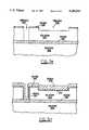
- FIG. 1shows such a bonded wafer 100 in cross sectional elevation view with silicon-on-insulator layer 102, oxide insulation layer 104, handle wafer 106. Deep isolation trenches 110 also appear in FIG. 1 with oxide 108 coated sidewalls and filled with polysilicon 112.
- a thick oxide layermay be used between the extrinsic base and the collector. In order to minimize surface undulation, this oxide is completely recessed.
- the method of fabricating such an oxide layeris the well known LOCOS technology. LOCOS technology, however, is not capable of producing a completely recessed oxide.
- the Bird's Beakis a lateral encroachment by the oxide, resulting in larger than necessary recessed oxide.
- the consequence of the Bird's Beakis that the contact areas of the base and collector of the bipolar transistor has to be increased, thus increasing the size of the whole transistor. It is known that by decreasing the transistor dimensions the high frequency performance of the transistor will increase. Therefore it is very important to minimize or completely eliminate the Bird's Head and Bird's Beak from the recessed oxide. Further, the growth of LOCOS oxide yields a stressed oxide which limits the thickness that can be tolerated.
- the present inventionprovides recessed isolation oxide for both bipolar and field effect devices with both deep and shallow isolation trenches which are simultaneously filled and planarized. This eliminates the typical shallow trench Bird's Head and Bird's Beak of LOCOS without excessive processing steps and in conjunction with deep trench processing. Further, it is compatible with bonded wafer processing as well as conventional processing.
- FIGS. 1-2illustrate in cross sectional elevation views known bonded wafers with trench and LOCOS isolation
- FIGS. 3a-kare cross sectional elevation views of a first preferred embodiment method of isolation compatible with bonded wafer processing
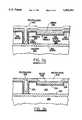
- FIGS. 4is a cross sectional elevation view of a bipolar transistor fabricated in an isolated wafer using the preferred embodiment method
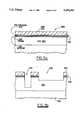
- FIGS. 5a-fare cross sectional elevation views of a fourth preferred embodiment.
- FIG. 6illustrates another preferred embodiment method in cross sectional elevation view.
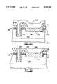
- FIGS. 3a-killustrate in cross sectional elevation views the steps of a first preferred embodiment method of isolation in the example of bipolar transistor fabrication in bonded wafer processing. Other substrates could be used with essentially the same method steps. The method proceeds as follows:
- a 4-inch diameter bonded silicon wafer 300which includes silicon-on-insulator device layer 302 of doping type and resistivity (e.g., N type and 6-20 ohm-cm resistivity) desired for eventual device fabrication and with thickness of about 6 ⁇ m, bottom oxide 304 of thickness 2 ⁇ m, and handle wafer 306 of typical wafer thickness 525 ⁇ m.
- doping type and resistivitye.g., N type and 6-20 ohm-cm resistivity
- handle wafer 306of typical wafer thickness 525 ⁇ m.
- other diameters, resistivities, and thicknessescould be used.
- the eventual buried layerwould be formed by doping the device wafer 302 on the face to be oxidized to bottom oxide 304.
- the methods of Delgado and Bajor, U.S. Pat. No, 4,897,362could be used to provide selective buried layers. See FIG. 3a.
- TEOStetraethoxyorthosilicate
- polish excess polysilicon 340 from the surface above TEOS oxide 338 to form a planar top surfaceThis polishing may be performed mechanically with alumina and diamond powder slurries or with the addition of a silicon etchant. See FIG. 3h.
- This plasma etch processcan be adjusted to etch photoresist 350 and oxide 338 with the same etch rate. Because the photoresist surface is expected to be practically planar, this etch will planarize the oxide. See FIG. 3k which shows the result of the plasma etch once oxide 326 has been cleared from silicon layer 302. Trenches 310 partition silicon layer 302 into islands, and recessed oxides (made of about 1 ⁇ m of TEOS oxide 338 on 500 ⁇ of thermal oxide 334) have been formed in the shallow trenches 330 in the islands.
- photoresist printing in step (d)determines the size and location of recessed oxide trenches 330 without any Bird's Head or Bird's Beak effects. On large area shallow trenches the photoresist will not have a flat surface, as shown in FIG. 3j, but will follow the surface of the shallow trench. This will prevent using photoresist planarization for large area shallow trenches.
- Fabricate devices in the silicon islandsThe particular fabrication steps used will depend upon the types of devices, interconnection structure, and insulations desired and can include oxide growth and deposition, photoresist patterning, wet and dry etches, diffusions and implants, various material depositions such as polysilicon and silicon nitride, epitaxial layer growth, deposition of various metals such as aluminum an tungsten, and chemomechanical polishing.
- FIG. 4schematically shows in cross sectional elevation view a bipolar transistor with shallow trench isolation between the collector contact and the intrinsic base and deep trench isolation about the periphery.
- a second preferred embodiment method of isolationfollows the steps of the first preferred embodiment method except step (e) is changed to the following step (e 2 ) in which the patterned photoresist remains to protect the deep trench sidewalls.
- the photoresistwill protect the deep trenches provided that the deep trenches are as narrow as 2 ⁇ m:
- the patterned photoresist 328 plus oxide 326serve as the etch mask with photoresist 328 protecting the sidewalls of trenches 310. Then strip photoresist 328.
- step (f) of the first preferred embodiment method
- a third preferred embodiment method of isolationfollows the steps of the first preferred embodiment method except steps (d)-(e) are changed to the following steps (d 3 )-(e 3 ) which replace mask oxide 326 with a new oxide for deep trench sidewall protection during the shallow trench etch:
- (d 3 )Strip patterned oxide 326, and thermally grow thin (500 ⁇ ) oxide to provide a good oxide-silicon interface.
- step (f) of the first preferred embodiment method
- a fourth preferred embodiment method of isolationroughly follows the steps of any of the first three preferred embodiment methods except a multilayer of oxide, silicon nitride (optional), and polysilicon replaces oxide layer 326.
- the steps of the fourth preferred embodiment methodare illustrated in FIGS. 5a-f for the example of bulk silicon as follows:
- a 6-inch diameter silicon wafer 500which includes epitaxial device layer 502.
- a 1000 ⁇ layer 521 of silicon nitride(“nitride”) could be deposited on oxide 520 before deposition of polysilicon 522 and USG 524.
- This multilayer 526 of oxide 520, nitride 521, and polysilicon 522 plus USG 524will be used as a trench etch mask. See FIG. 5a which shows multilayer 526 with the nitride option.
- Polish excess polysilicon 540 from the surface above TEOS oxide 538 to form a planar top surfaceThis polysilicon polish may be performed with fine diamond grit in a slurry containing a silicon etchant. The removal rate of oxide is much less than that of polysilicon, and thus the polishing can be effectively stopped. See FIG. 5d.
- the polysilicon sublayer 522 of the multilayer 526will act as an etch stop.
- the polysilicon trench fill 540will mask both oxide 538 in the deep and shallow trenches and also a small area of the oxide at the perimeter of the trenches, thus creating oxide stringers 550 above the wafer surface. See FIG. 5e.
- the oxide etchis self-aligned to the trenches by polysilicon 540 in the trenches.
- the top of the polysilicon fill 540is higher than the surface of multilayer 526.
- the differenceis the thickness of TEOS layer 538.
- These polysilicon islands that are sticking out form the surface (as mesas)are surrounded with oxide stringers 550.
- step (h)Fabricate devices in the silicon islands as in step (l) of the first preferred embodiment.
- the fifth preferred embodiment methodfollows the steps of the fourth preferred embodiment method except the planarization of steps (f)-(g) is replaced by a polish planarization.
- Polish planarizationcan be used to remove the polysilicon 540 mesas together with the polysilicon layer 522 of multilayer 526.
- the bottom oxide layer 520 of the multilayerwill act as a polish-stop, because the polysilicon polishing rate is significantly larger than that of the oxide layer 520. Since the area of the oxide stringers is very small compared to the polysilicon mesa area, the presence of the stringers will practically not influence the polishing rate of the polysilicon mesas. Also, the fact that the stringers protrude from the wafer surface implies the polishing eliminates them despite the slow removal rate of oxide.
- Optional nitride layer 521can also be used as a polish stop since the polishing selectivity between the polysilicon and the silicon nitride is larger than the selectivity between the polysilicon and the oxide.
- FIG. 6shows wafer 500 with nitride layer 521 after polishing.
- the preferred embodiment methodshave the advantages of eliminating the Bird's Head and Bird's Beak of LOCOS, and also the stress generated by grown oxide. Indeed, the thin thermal oxide coating of the deep and shallow trenches provides the good electrical interface, and the deposited oxide provides insulation without grown oxide stresses. Further, the shallow trenches may be placed anywhere on the device layer, including overlapping the deep trenches.
- the planarization using the multilayer as in FIGS. 5d-f and 6,is self-aligned and could be used even without the deep trenches. That is, trenches may be filled with a conformal oxide (or other dielectric) deposition and this is followed by a conformal polysilicon deposition over the oxide and a polysilicon planarization to leave polysilicon on the oxide only over the trenches. Thus the oxide in the trenches is masked by the polysilicon in a self-aligned manner, and an oxide etch can selectively remove the oxide outside of the trenches.
- the preferred embodiment methodsmay be varied in many ways while retaining one or more of the features of deep filled trench isolation and shallow filled trench isolation formed together and use of self-aligned trench dielectric removal.
- various deep trench etching methodscould be used, including ECR plasma and redeposition plasma to provide a slight taper in the trenches.
- the deep trenchescould be filled entirely with insulator.
- the dimensionscould be varied over a large range: the silicon-on-insulator layer thickness could vary between a few ⁇ m and 100 ⁇ m, the shallow trenches could vary between a few thousand ⁇ and a few ⁇ m, the deep trenches need not extend fully to any bottom oxide, the bottoms of the trenches could be doped for channel stops, the wafer diameter may be any size such as two inches or greater than eight inches.
- nitridecould fill or partially fill the trenches, and the polysilicon fill could be a different material with an etch selectivity with respect to the first material deposited in the trenches.
- the bottom oxidecould an agglomeration of various insulators such as nitride, sapphire, glasses and may even include conductors.
- the thermal oxide coating of the trenchescould be omitted.
- Other material systemscould be used, such as gallium arsenide bonded to silicon with nitride insulator.
Landscapes
- Engineering & Computer Science (AREA)
- Physics & Mathematics (AREA)
- Condensed Matter Physics & Semiconductors (AREA)
- General Physics & Mathematics (AREA)
- Manufacturing & Machinery (AREA)
- Computer Hardware Design (AREA)
- Microelectronics & Electronic Packaging (AREA)
- Power Engineering (AREA)
- Chemical & Material Sciences (AREA)
- Crystallography & Structural Chemistry (AREA)
- Element Separation (AREA)
Abstract
Description
Claims (9)
Priority Applications (3)
| Application Number | Priority Date | Filing Date | Title |
|---|---|---|---|
| US07/935,765US5382541A (en) | 1992-08-26 | 1992-08-26 | Method for forming recessed oxide isolation containing deep and shallow trenches |
| PCT/US1993/008017WO1994005037A1 (en) | 1992-08-26 | 1993-08-26 | Recessed oxide and method |
| US08/339,966US5504033A (en) | 1992-08-26 | 1994-11-15 | Method for forming recessed oxide isolation containing deep and shallow trenches |
Applications Claiming Priority (1)
| Application Number | Priority Date | Filing Date | Title |
|---|---|---|---|
| US07/935,765US5382541A (en) | 1992-08-26 | 1992-08-26 | Method for forming recessed oxide isolation containing deep and shallow trenches |
Related Child Applications (1)
| Application Number | Title | Priority Date | Filing Date |
|---|---|---|---|
| US08/339,966DivisionUS5504033A (en) | 1992-08-26 | 1994-11-15 | Method for forming recessed oxide isolation containing deep and shallow trenches |
Publications (1)
| Publication Number | Publication Date |
|---|---|
| US5382541Atrue US5382541A (en) | 1995-01-17 |
Family
ID=25467628
Family Applications (2)
| Application Number | Title | Priority Date | Filing Date |
|---|---|---|---|
| US07/935,765Expired - LifetimeUS5382541A (en) | 1992-08-26 | 1992-08-26 | Method for forming recessed oxide isolation containing deep and shallow trenches |
| US08/339,966Expired - LifetimeUS5504033A (en) | 1992-08-26 | 1994-11-15 | Method for forming recessed oxide isolation containing deep and shallow trenches |
Family Applications After (1)
| Application Number | Title | Priority Date | Filing Date |
|---|---|---|---|
| US08/339,966Expired - LifetimeUS5504033A (en) | 1992-08-26 | 1994-11-15 | Method for forming recessed oxide isolation containing deep and shallow trenches |
Country Status (2)
| Country | Link |
|---|---|
| US (2) | US5382541A (en) |
| WO (1) | WO1994005037A1 (en) |
Cited By (23)
| Publication number | Priority date | Publication date | Assignee | Title |
|---|---|---|---|---|
| US5472904A (en)* | 1994-03-02 | 1995-12-05 | Micron Technology, Inc. | Thermal trench isolation |
| US5721173A (en)* | 1997-02-25 | 1998-02-24 | Kabushiki Kaisha Toshiba | Method of forming a shallow trench isolation structure |
| US5837596A (en)* | 1994-03-02 | 1998-11-17 | Micron Technology, Inc. | Field oxide formation by oxidation of polysilicon layer |
| US5914280A (en)* | 1996-12-23 | 1999-06-22 | Harris Corporation | Deep trench etch on bonded silicon wafer |
| US5994201A (en)* | 1998-07-14 | 1999-11-30 | United Microelectronics Corp. | Method for manufacturing shallow trench isolation regions |
| US6326288B1 (en)* | 1999-07-06 | 2001-12-04 | Elmos Semiconductor Ag | CMOS compatible SOI process |
| US6436611B1 (en)* | 1999-07-07 | 2002-08-20 | Samsung Electronics Co., Ltd. | Trench isolation method for semiconductor integrated circuit |
| US6440819B1 (en)* | 1998-03-03 | 2002-08-27 | Advanced Micro Devices, Inc. | Method for differential trenching in conjunction with differential fieldox growth |
| US6475875B1 (en) | 2001-07-09 | 2002-11-05 | Chartered Semiconductor Manufacturing Ltd. | Shallow trench isolation elevation uniformity via insertion of a polysilicon etch layer |
| US6518641B2 (en) | 2001-05-18 | 2003-02-11 | International Business Machines Corporation | Deep slit isolation with controlled void |
| US6593210B1 (en)* | 2000-10-24 | 2003-07-15 | Advanced Micro Devices, Inc. | Self-aligned/maskless reverse etch process using an inorganic film |
| US20040058508A1 (en)* | 2002-05-07 | 2004-03-25 | Krishna Parat | Dual trench isolation using single critical lithographic patterning |
| US6756654B2 (en)* | 2001-08-09 | 2004-06-29 | Samsung Electronics Co., Ltd. | Structure of trench isolation and a method of forming the same |
| US20050124134A1 (en)* | 2003-12-08 | 2005-06-09 | Nanya Technology Corporation | STI forming method for improving STI step uniformity |
| GB2372631B (en)* | 2001-02-22 | 2005-08-03 | Mitel Semiconductor Ltd | Semiconductor-on-insulator structure |
| US20070158725A1 (en)* | 2006-01-09 | 2007-07-12 | International Business Machines Corporation | Semiconductor structure including trench capacitor and trench resistor |
| US20070254452A1 (en)* | 2006-04-26 | 2007-11-01 | Luigi Merlin | Mask structure for manufacture of trench type semiconductor device |
| US20090045468A1 (en)* | 2007-08-16 | 2009-02-19 | Terence Blackwell Hook | Trench isolation and method of fabricating trench isolation |
| US20100203703A1 (en)* | 2005-05-10 | 2010-08-12 | Armin Tilke | Deep Trench Isolation Structures and Methods of Formation Thereof |
| US20150021623A1 (en)* | 2013-07-17 | 2015-01-22 | Cree, Inc. | Enhanced gate dielectric for a field effect device with a trenched gate |
| US20160276210A1 (en)* | 2015-03-19 | 2016-09-22 | Globalfoundries Singapore Pte. Ltd. | Integrated circuits using silicon on insulator substrates and methods of manufacturing the same |
| US20170186693A1 (en)* | 2015-12-29 | 2017-06-29 | Globalfoundries Inc. | Soi wafers with buried dielectric layers to prevent cu diffusion |
| US9893157B1 (en) | 2017-01-09 | 2018-02-13 | Globalfoundries Inc. | Structures with contact trenches and isolation trenches |
Families Citing this family (51)
| Publication number | Priority date | Publication date | Assignee | Title |
|---|---|---|---|---|
| JP2644912B2 (en) | 1990-08-29 | 1997-08-25 | 株式会社日立製作所 | Vacuum processing apparatus and operating method thereof |
| USD453402S1 (en) | 1990-08-22 | 2002-02-05 | Hitachi, Ltd. | Vacuum processing equipment configuration |
| US7089680B1 (en) | 1990-08-29 | 2006-08-15 | Hitachi, Ltd. | Vacuum processing apparatus and operating method therefor |
| USD473354S1 (en) | 1990-08-29 | 2003-04-15 | Hitachi, Ltd. | Vacuum processing equipment configuration |
| USRE39756E1 (en)* | 1990-08-29 | 2007-08-07 | Hitachi, Ltd. | Vacuum processing operating method with wafers, substrates and/or semiconductors |
| USRE39824E1 (en)* | 1990-08-29 | 2007-09-11 | Hitachi, Ltd. | Vacuum processing apparatus and operating method with wafers, substrates and/or semiconductors |
| US5411913A (en)* | 1994-04-29 | 1995-05-02 | National Semiconductor Corporation | Simple planarized trench isolation and field oxide formation using poly-silicon |
| US5661073A (en)* | 1995-08-11 | 1997-08-26 | Micron Technology, Inc. | Method for forming field oxide having uniform thickness |
| US5614431A (en)* | 1995-12-20 | 1997-03-25 | International Business Machines Corporation | Method of making buried strap trench cell yielding an extended transistor |
| TW309647B (en)* | 1995-12-30 | 1997-07-01 | Hyundai Electronics Ind | |
| US5843226A (en)* | 1996-07-16 | 1998-12-01 | Applied Materials, Inc. | Etch process for single crystal silicon |
| US5923991A (en)* | 1996-11-05 | 1999-07-13 | International Business Machines Corporation | Methods to prevent divot formation in shallow trench isolation areas |
| KR100226736B1 (en)* | 1996-11-07 | 1999-10-15 | 구본준 | Isolation Area Formation Method |
| US6103592A (en)* | 1997-05-01 | 2000-08-15 | International Business Machines Corp. | Manufacturing self-aligned polysilicon fet devices isolated with maskless shallow trench isolation and gate conductor fill technology with active devices and dummy doped regions formed in mesas |
| US6150072A (en)* | 1997-08-22 | 2000-11-21 | Siemens Microelectronics, Inc. | Method of manufacturing a shallow trench isolation structure for a semiconductor device |
| JP4187808B2 (en)* | 1997-08-25 | 2008-11-26 | 株式会社ルネサステクノロジ | Manufacturing method of semiconductor device |
| DE19751740B4 (en)* | 1997-11-21 | 2005-03-10 | Infineon Technologies Ag | Process for the production of an integrated circuit with different deep isolation trenches |
| JP3519589B2 (en) | 1997-12-24 | 2004-04-19 | 株式会社ルネサステクノロジ | Manufacturing method of semiconductor integrated circuit |
| US6133610A (en) | 1998-01-20 | 2000-10-17 | International Business Machines Corporation | Silicon-on-insulator chip having an isolation barrier for reliability and process of manufacture |
| US6492684B2 (en) | 1998-01-20 | 2002-12-10 | International Business Machines Corporation | Silicon-on-insulator chip having an isolation barrier for reliability |
| US6121659A (en)* | 1998-03-27 | 2000-09-19 | International Business Machines Corporation | Buried patterned conductor planes for semiconductor-on-insulator integrated circuit |
| KR20000040104A (en)* | 1998-12-17 | 2000-07-05 | 김영환 | Method for manufacturing silicon-on-insulator wafer |
| US6180486B1 (en)* | 1999-02-16 | 2001-01-30 | International Business Machines Corporation | Process of fabricating planar and densely patterned silicon-on-insulator structure |
| US6048775A (en)* | 1999-05-24 | 2000-04-11 | Vanguard International Semiconductor Corporation | Method to make shallow trench isolation structure by HDP-CVD and chemical mechanical polish processes |
| US6372600B1 (en)* | 1999-08-30 | 2002-04-16 | Agere Systems Guardian Corp. | Etch stops and alignment marks for bonded wafers |
| EP1104023A1 (en) | 1999-11-26 | 2001-05-30 | STMicroelectronics S.r.l. | Process for manufacturing electronic devices comprising non-volatile memory cells |
| US6830988B1 (en)* | 2000-01-06 | 2004-12-14 | National Semiconductor Corporation | Method of forming an isolation structure for an integrated circuit utilizing grown and deposited oxide |
| US6396121B1 (en)* | 2000-05-31 | 2002-05-28 | International Business Machines Corporation | Structures and methods of anti-fuse formation in SOI |
| JP2002076113A (en) | 2000-08-31 | 2002-03-15 | Matsushita Electric Ind Co Ltd | Semiconductor device and method of manufacturing the same |
| US6667226B2 (en)* | 2000-12-22 | 2003-12-23 | Texas Instruments Incorporated | Method and system for integrating shallow trench and deep trench isolation structures in a semiconductor device |
| US6787422B2 (en)* | 2001-01-08 | 2004-09-07 | Chartered Semiconductor Manufacturing Ltd. | Method of body contact for SOI mosfet |
| KR100389031B1 (en)* | 2001-06-19 | 2003-06-25 | 삼성전자주식회사 | Method of fabricating semiconductor device having trench isolation structure |
| FR2828579B1 (en)* | 2001-08-13 | 2004-01-30 | St Microelectronics Sa | PROCESS FOR HANDLING A THIN SILICON WAFER |
| US6649460B2 (en)* | 2001-10-25 | 2003-11-18 | International Business Machines Corporation | Fabricating a substantially self-aligned MOSFET |
| JP2003243662A (en)* | 2002-02-14 | 2003-08-29 | Mitsubishi Electric Corp | Semiconductor device and manufacturing method thereof, semiconductor wafer |
| KR100427538B1 (en)* | 2002-06-04 | 2004-04-28 | 주식회사 하이닉스반도체 | Method of forming a isolation layer in a semiconductor device |
| US6864151B2 (en)* | 2003-07-09 | 2005-03-08 | Infineon Technologies Ag | Method of forming shallow trench isolation using deep trench isolation |
| DE10345346B4 (en)* | 2003-09-19 | 2010-09-16 | Atmel Automotive Gmbh | A method of manufacturing a semiconductor device having active regions separated by isolation structures |
| DE10345345A1 (en)* | 2003-09-19 | 2005-04-14 | Atmel Germany Gmbh | Method of manufacturing semiconductor devices in a semiconductor substrate |
| US20070054464A1 (en)* | 2005-09-08 | 2007-03-08 | Chartered Semiconductor Manufacturing Ltd. | Different STI depth for Ron improvement for LDMOS integration with submicron devices |
| US7811935B2 (en)* | 2006-03-07 | 2010-10-12 | Micron Technology, Inc. | Isolation regions and their formation |
| KR100876806B1 (en)* | 2006-07-20 | 2009-01-07 | 주식회사 하이닉스반도체 | Transistor Formation Method of Semiconductor Device Using Double Patterning Technology |
| US8163621B2 (en) | 2008-06-06 | 2012-04-24 | Globalfoundries Singapore Pte. Ltd. | High performance LDMOS device having enhanced dielectric strain layer |
| CN101677058B (en)* | 2008-09-19 | 2012-02-29 | 北京京东方光电科技有限公司 | Manufacturing method of thin film structure |
| US8071461B2 (en)* | 2008-12-04 | 2011-12-06 | Freescale Semiconductor, Inc. | Low loss substrate for integrated passive devices |
| US7998852B2 (en) | 2008-12-04 | 2011-08-16 | Freescale Semiconductor, Inc. | Methods for forming an RF device with trench under bond pad feature |
| US20110115047A1 (en)* | 2009-11-13 | 2011-05-19 | Francois Hebert | Semiconductor process using mask openings of varying widths to form two or more device structures |
| US8525292B2 (en) | 2011-04-17 | 2013-09-03 | International Business Machines Corporation | SOI device with DTI and STI |
| US8994085B2 (en) | 2012-01-06 | 2015-03-31 | International Business Machines Corporation | Integrated circuit including DRAM and SRAM/logic |
| KR102277398B1 (en)* | 2014-09-17 | 2021-07-16 | 삼성전자주식회사 | A semiconductor device and method of fabricating the same |
| US11239315B2 (en) | 2020-02-03 | 2022-02-01 | Globalfoundries U.S. Inc. | Dual trench isolation structures |
Citations (9)
| Publication number | Priority date | Publication date | Assignee | Title |
|---|---|---|---|---|
| EP0120614A1 (en)* | 1983-02-28 | 1984-10-03 | Oki Electric Industry Company, Limited | Method of manufacturing a semiconductor device having isolation regions |
| JPS61228650A (en)* | 1985-04-02 | 1986-10-11 | Sony Corp | Manufacture of semiconductor device |
| JPS61256649A (en)* | 1985-05-09 | 1986-11-14 | Nec Corp | Formation of element isolation region |
| EP0300569A1 (en)* | 1987-07-21 | 1989-01-25 | Koninklijke Philips Electronics N.V. | Method of manufacturing a semiconductor device having a planarized construction |
| JPH0254556A (en)* | 1988-08-18 | 1990-02-23 | Oki Electric Ind Co Ltd | Manufacture of semiconductor integrated circuit device |
| EP0398468A2 (en)* | 1989-05-16 | 1990-11-22 | Kabushiki Kaisha Toshiba | Dielectrically isolated substrate and semiconductor device using the same |
| EP0405923A2 (en)* | 1989-06-30 | 1991-01-02 | Samsung Electronics Co., Ltd. | Method for forming variable width isolation structures |
| EP0424608A1 (en)* | 1989-10-25 | 1991-05-02 | International Business Machines Corporation | Forming wide dielectric filled isolation trenches in semiconductors |
| US5173439A (en)* | 1989-10-25 | 1992-12-22 | International Business Machines Corporation | Forming wide dielectric-filled isolation trenches in semi-conductors |
Family Cites Families (9)
| Publication number | Priority date | Publication date | Assignee | Title |
|---|---|---|---|---|
| JPS58169933A (en)* | 1982-03-30 | 1983-10-06 | Fujitsu Ltd | Manufacture of semiconductor device |
| JPS6032338A (en)* | 1983-08-02 | 1985-02-19 | Oki Electric Ind Co Ltd | Manufacture of semiconductor element |
| JPS61289642A (en)* | 1985-06-18 | 1986-12-19 | Matsushita Electric Ind Co Ltd | Method for manufacturing semiconductor integrated circuit device |
| JPH01106466A (en)* | 1987-10-19 | 1989-04-24 | Fujitsu Ltd | Manufacturing method of semiconductor device |
| JPH01309373A (en)* | 1988-06-07 | 1989-12-13 | Nec Corp | Manufacture of semiconductor device |
| JPH0290617A (en)* | 1988-09-28 | 1990-03-30 | Nec Corp | Manufacture of semiconductor device |
| JPH03218049A (en)* | 1990-01-23 | 1991-09-25 | Sony Corp | Manufacture of semiconductor device |
| JPH0775245B2 (en)* | 1990-11-16 | 1995-08-09 | 信越半導体株式会社 | Dielectric isolation substrate and manufacturing method thereof |
| US5270265A (en)* | 1992-09-01 | 1993-12-14 | Harris Corporation | Stress relief technique of removing oxide from surface of trench-patterned semiconductor-on-insulator structure |
- 1992
- 1992-08-26USUS07/935,765patent/US5382541A/ennot_activeExpired - Lifetime
- 1993
- 1993-08-26WOPCT/US1993/008017patent/WO1994005037A1/enactiveApplication Filing
- 1994
- 1994-11-15USUS08/339,966patent/US5504033A/ennot_activeExpired - Lifetime
Patent Citations (9)
| Publication number | Priority date | Publication date | Assignee | Title |
|---|---|---|---|---|
| EP0120614A1 (en)* | 1983-02-28 | 1984-10-03 | Oki Electric Industry Company, Limited | Method of manufacturing a semiconductor device having isolation regions |
| JPS61228650A (en)* | 1985-04-02 | 1986-10-11 | Sony Corp | Manufacture of semiconductor device |
| JPS61256649A (en)* | 1985-05-09 | 1986-11-14 | Nec Corp | Formation of element isolation region |
| EP0300569A1 (en)* | 1987-07-21 | 1989-01-25 | Koninklijke Philips Electronics N.V. | Method of manufacturing a semiconductor device having a planarized construction |
| JPH0254556A (en)* | 1988-08-18 | 1990-02-23 | Oki Electric Ind Co Ltd | Manufacture of semiconductor integrated circuit device |
| EP0398468A2 (en)* | 1989-05-16 | 1990-11-22 | Kabushiki Kaisha Toshiba | Dielectrically isolated substrate and semiconductor device using the same |
| EP0405923A2 (en)* | 1989-06-30 | 1991-01-02 | Samsung Electronics Co., Ltd. | Method for forming variable width isolation structures |
| EP0424608A1 (en)* | 1989-10-25 | 1991-05-02 | International Business Machines Corporation | Forming wide dielectric filled isolation trenches in semiconductors |
| US5173439A (en)* | 1989-10-25 | 1992-12-22 | International Business Machines Corporation | Forming wide dielectric-filled isolation trenches in semi-conductors |
Non-Patent Citations (8)
| Title |
|---|
| H. Nishizawa, et al., "1991 Symposium on VLSI Technology Digest of Technical Papers," Institute of Electrical & Electronics Engineers Procedings of the Symposium on VLSI Technology, pp. 51-52, (1991). |
| H. Nishizawa, et al., 1991 Symposium on VLSI Technology Digest of Technical Papers, Institute of Electrical & Electronics Engineers Procedings of the Symposium on VLSI Technology, pp. 51 52, (1991).* |
| IBM Technical Disclosure Bulletin, vol. 33, No. 4, Sep. 1990, New York U.S. pp. 210 212, Shallow Trench Formation Using Polysilicon Trench Refill .* |
| IBM Technical Disclosure Bulletin, vol. 33, No. 4, Sep. 1990, New York U.S. pp. 210-212, "Shallow Trench Formation Using Polysilicon Trench Refill". |
| Patent Abstracts of Japan, vol. 009, No. 150 (E 324) (1873) Jun. 25, 1985.* |
| Patent Abstracts of Japan, vol. 009, No. 150 (E-324) (1873) Jun. 25, 1985. |
| Patent Abstracts of Japan, vol. 015, No. 498 (E 1146) Dec. 17, 1991.* |
| Patent Abstracts of Japan, vol. 015, No. 498 (E-1146) Dec. 17, 1991. |
Cited By (43)
| Publication number | Priority date | Publication date | Assignee | Title |
|---|---|---|---|---|
| US5888881A (en)* | 1994-03-02 | 1999-03-30 | Micron Technology, Inc. | Method of trench isolation during the formation of a semiconductor device |
| US5472904A (en)* | 1994-03-02 | 1995-12-05 | Micron Technology, Inc. | Thermal trench isolation |
| US5837596A (en)* | 1994-03-02 | 1998-11-17 | Micron Technology, Inc. | Field oxide formation by oxidation of polysilicon layer |
| US6198150B1 (en) | 1996-12-23 | 2001-03-06 | Intersil Corporation | Integrated circuit with deep trench having multiple slopes |
| US5914280A (en)* | 1996-12-23 | 1999-06-22 | Harris Corporation | Deep trench etch on bonded silicon wafer |
| US5721173A (en)* | 1997-02-25 | 1998-02-24 | Kabushiki Kaisha Toshiba | Method of forming a shallow trench isolation structure |
| US6440819B1 (en)* | 1998-03-03 | 2002-08-27 | Advanced Micro Devices, Inc. | Method for differential trenching in conjunction with differential fieldox growth |
| US5994201A (en)* | 1998-07-14 | 1999-11-30 | United Microelectronics Corp. | Method for manufacturing shallow trench isolation regions |
| US6326288B1 (en)* | 1999-07-06 | 2001-12-04 | Elmos Semiconductor Ag | CMOS compatible SOI process |
| US6436611B1 (en)* | 1999-07-07 | 2002-08-20 | Samsung Electronics Co., Ltd. | Trench isolation method for semiconductor integrated circuit |
| US6593210B1 (en)* | 2000-10-24 | 2003-07-15 | Advanced Micro Devices, Inc. | Self-aligned/maskless reverse etch process using an inorganic film |
| GB2372631B (en)* | 2001-02-22 | 2005-08-03 | Mitel Semiconductor Ltd | Semiconductor-on-insulator structure |
| US6518641B2 (en) | 2001-05-18 | 2003-02-11 | International Business Machines Corporation | Deep slit isolation with controlled void |
| US6475875B1 (en) | 2001-07-09 | 2002-11-05 | Chartered Semiconductor Manufacturing Ltd. | Shallow trench isolation elevation uniformity via insertion of a polysilicon etch layer |
| US7160787B2 (en) | 2001-08-09 | 2007-01-09 | Samsung Electronics Co., Ltd. | Structure of trench isolation and a method of forming the same |
| US20040171271A1 (en)* | 2001-08-09 | 2004-09-02 | Samsung Electronics Co., Ltd. | Structure of trench isolation and a method of forming the same |
| US6756654B2 (en)* | 2001-08-09 | 2004-06-29 | Samsung Electronics Co., Ltd. | Structure of trench isolation and a method of forming the same |
| US6949801B2 (en)* | 2002-05-07 | 2005-09-27 | Intel Corporation | Dual trench isolation using single critical lithographic patterning |
| US20040058508A1 (en)* | 2002-05-07 | 2004-03-25 | Krishna Parat | Dual trench isolation using single critical lithographic patterning |
| US20050124134A1 (en)* | 2003-12-08 | 2005-06-09 | Nanya Technology Corporation | STI forming method for improving STI step uniformity |
| US7071075B2 (en)* | 2003-12-08 | 2006-07-04 | Nanya Technology Corporation | STI forming method for improving STI step uniformity |
| US20100203703A1 (en)* | 2005-05-10 | 2010-08-12 | Armin Tilke | Deep Trench Isolation Structures and Methods of Formation Thereof |
| US8258028B2 (en)* | 2005-05-10 | 2012-09-04 | Infineon Technologies Ag | Deep trench isolation structures and methods of formation thereof |
| TWI392080B (en)* | 2006-01-09 | 2013-04-01 | Ibm | Semiconductor structure with trench capacitance and trench resistance |
| US7560761B2 (en)* | 2006-01-09 | 2009-07-14 | International Business Machines Corporation | Semiconductor structure including trench capacitor and trench resistor |
| US20090267186A1 (en)* | 2006-01-09 | 2009-10-29 | International Business Machines Corporation | Semiconductor structure including trench capacitor and trench resistor |
| US8110862B2 (en) | 2006-01-09 | 2012-02-07 | International Business Machines Corporation | Semiconductor structure including trench capacitor and trench resistor |
| US20070158725A1 (en)* | 2006-01-09 | 2007-07-12 | International Business Machines Corporation | Semiconductor structure including trench capacitor and trench resistor |
| US20070254452A1 (en)* | 2006-04-26 | 2007-11-01 | Luigi Merlin | Mask structure for manufacture of trench type semiconductor device |
| WO2007127197A3 (en)* | 2006-04-26 | 2008-07-10 | Int Rectifier Corp | Mask structure for manufacture of trench type semiconductor device |
| US7808029B2 (en) | 2006-04-26 | 2010-10-05 | Siliconix Technology C.V. | Mask structure for manufacture of trench type semiconductor device |
| US8012848B2 (en)* | 2007-08-16 | 2011-09-06 | International Business Machines Corporation | Trench isolation and method of fabricating trench isolation |
| US20110278674A1 (en)* | 2007-08-16 | 2011-11-17 | International Business Machines Corporation | Trench isolation and method of fabricating trench isolation |
| US20090045468A1 (en)* | 2007-08-16 | 2009-02-19 | Terence Blackwell Hook | Trench isolation and method of fabricating trench isolation |
| US20150021623A1 (en)* | 2013-07-17 | 2015-01-22 | Cree, Inc. | Enhanced gate dielectric for a field effect device with a trenched gate |
| US9570570B2 (en)* | 2013-07-17 | 2017-02-14 | Cree, Inc. | Enhanced gate dielectric for a field effect device with a trenched gate |
| US20160276210A1 (en)* | 2015-03-19 | 2016-09-22 | Globalfoundries Singapore Pte. Ltd. | Integrated circuits using silicon on insulator substrates and methods of manufacturing the same |
| US9922868B2 (en)* | 2015-03-19 | 2018-03-20 | Globalfoundries Singapore Pte. Ltd. | Integrated circuits using silicon on insulator substrates and methods of manufacturing the same |
| US20170186693A1 (en)* | 2015-12-29 | 2017-06-29 | Globalfoundries Inc. | Soi wafers with buried dielectric layers to prevent cu diffusion |
| US9806025B2 (en)* | 2015-12-29 | 2017-10-31 | Globalfoundries Inc. | SOI wafers with buried dielectric layers to prevent Cu diffusion |
| US10242947B2 (en) | 2015-12-29 | 2019-03-26 | Globalfoundries Inc. | SOI wafers with buried dielectric layers to prevent CU diffusion |
| US10923427B2 (en) | 2015-12-29 | 2021-02-16 | Globalfoundries U.S. Inc. | SOI wafers with buried dielectric layers to prevent CU diffusion |
| US9893157B1 (en) | 2017-01-09 | 2018-02-13 | Globalfoundries Inc. | Structures with contact trenches and isolation trenches |
Also Published As
| Publication number | Publication date |
|---|---|
| WO1994005037A1 (en) | 1994-03-03 |
| US5504033A (en) | 1996-04-02 |
Similar Documents
| Publication | Publication Date | Title |
|---|---|---|
| US5382541A (en) | Method for forming recessed oxide isolation containing deep and shallow trenches | |
| US5112772A (en) | Method of fabricating a trench structure | |
| EP0545263B1 (en) | Method of forming trench isolation having polishing step and method of manufacturing semiconductor device | |
| US5276338A (en) | Bonded wafer structure having a buried insulation layer | |
| US5313094A (en) | Thermal dissipation of integrated circuits using diamond paths | |
| US6211039B1 (en) | Silicon-on-insulator islands and method for their formation | |
| US6251734B1 (en) | Method for fabricating trench isolation and trench substrate contact | |
| US5262346A (en) | Nitride polish stop for forming SOI wafers | |
| US5318663A (en) | Method for thinning SOI films having improved thickness uniformity | |
| EP0609551B1 (en) | Method of planarizing a semiconductor device | |
| US5264387A (en) | Method of forming uniformly thin, isolated silicon mesas on an insulating substrate | |
| US6080628A (en) | Method of forming shallow trench isolation for integrated circuit applications | |
| WO1993019486A1 (en) | Method of forming semiconductor integrated circuit with polysilicon-filled trench isolation | |
| US6171929B1 (en) | Shallow trench isolator via non-critical chemical mechanical polishing | |
| EP0954022B1 (en) | Method for providing shallow trench isolation of transistors | |
| KR100234416B1 (en) | Method of forming a device isolation film of semiconductor device | |
| US6165869A (en) | Method to avoid dishing in forming trenches for shallow trench isolation | |
| US5923991A (en) | Methods to prevent divot formation in shallow trench isolation areas | |
| US6828213B2 (en) | Method to improve STI nano gap fill and moat nitride pull back | |
| US6548373B2 (en) | Method for forming shallow trench isolation structure | |
| US7041547B2 (en) | Methods of forming polished material and methods of forming isolation regions | |
| WO1993010559A1 (en) | Process for fabricating insulation-filled deep trenches in semiconductor substrates | |
| EP0878836B1 (en) | Planarising a semiconductor substrate | |
| KR100214530B1 (en) | Trench device isolation structure formation method | |
| US6436831B1 (en) | Methods of forming insulative plugs and oxide plug forming methods |
Legal Events
| Date | Code | Title | Description |
|---|---|---|---|
| AS | Assignment | Owner name:HARRIS CORPORATION, A CORP. OF DE, FLORIDA Free format text:ASSIGNMENT OF ASSIGNORS INTEREST.;ASSIGNORS:BAJOR, GEORGE;RIVOLI, ANTHONY L.;REEL/FRAME:006245/0968 Effective date:19920825 | |
| AS | Assignment | Owner name:SQUARE D COMPANY, ILLINOIS Free format text:ASSIGNMENT OF ASSIGNORS INTEREST.;ASSIGNORS:WONG, TAK M.;ETSHEIDT, RONALD J.;FREILINGER, PATRICK L.;REEL/FRAME:006334/0542 Effective date:19921113 | |
| STCF | Information on status: patent grant | Free format text:PATENTED CASE | |
| FEPP | Fee payment procedure | Free format text:PAYOR NUMBER ASSIGNED (ORIGINAL EVENT CODE: ASPN); ENTITY STATUS OF PATENT OWNER: LARGE ENTITY | |
| FPAY | Fee payment | Year of fee payment:4 | |
| AS | Assignment | Owner name:INTERSIL CORPORATION, FLORIDA Free format text:ASSIGNMENT OF ASSIGNORS INTEREST;ASSIGNOR:HARRIS CORPORATION;REEL/FRAME:010247/0043 Effective date:19990813 | |
| AS | Assignment | Owner name:CREDIT SUISSE FIRST BOSTON, AS COLLATERAL AGENT, N Free format text:SECURITY INTEREST;ASSIGNOR:INTERSIL CORPORATION;REEL/FRAME:010351/0410 Effective date:19990813 | |
| FPAY | Fee payment | Year of fee payment:8 | |
| REMI | Maintenance fee reminder mailed | ||
| FPAY | Fee payment | Year of fee payment:12 | |
| AS | Assignment | Owner name:MORGAN STANLEY & CO. INCORPORATED,NEW YORK Free format text:SECURITY AGREEMENT;ASSIGNORS:INTERSIL CORPORATION;TECHWELL, INC.;INTERSIL COMMUNICATIONS, INC.;AND OTHERS;REEL/FRAME:024390/0608 Effective date:20100427 | |
| AS | Assignment | Owner name:INTERSIL CORPORATION,FLORIDA Free format text:RELEASE BY SECURED PARTY;ASSIGNOR:CREDIT SUISSE FIRST BOSTON;REEL/FRAME:024445/0049 Effective date:20030306 |