US5382311A - Stage having electrostatic chuck and plasma processing apparatus using same - Google Patents
Stage having electrostatic chuck and plasma processing apparatus using sameDownload PDFInfo
- Publication number
- US5382311A US5382311AUS08/168,367US16836793AUS5382311AUS 5382311 AUS5382311 AUS 5382311AUS 16836793 AUS16836793 AUS 16836793AUS 5382311 AUS5382311 AUS 5382311A
- Authority
- US
- United States
- Prior art keywords
- groove
- electrostatic chuck
- stage
- gas
- substrate
- Prior art date
- Legal status (The legal status is an assumption and is not a legal conclusion. Google has not performed a legal analysis and makes no representation as to the accuracy of the status listed.)
- Expired - Lifetime
Links
Images


Classifications
- H—ELECTRICITY
- H01—ELECTRIC ELEMENTS
- H01L—SEMICONDUCTOR DEVICES NOT COVERED BY CLASS H10
- H01L21/00—Processes or apparatus adapted for the manufacture or treatment of semiconductor or solid state devices or of parts thereof
- H01L21/02—Manufacture or treatment of semiconductor devices or of parts thereof
- H01L21/04—Manufacture or treatment of semiconductor devices or of parts thereof the devices having potential barriers, e.g. a PN junction, depletion layer or carrier concentration layer
- H01L21/18—Manufacture or treatment of semiconductor devices or of parts thereof the devices having potential barriers, e.g. a PN junction, depletion layer or carrier concentration layer the devices having semiconductor bodies comprising elements of Group IV of the Periodic Table or AIIIBV compounds with or without impurities, e.g. doping materials
- H01L21/30—Treatment of semiconductor bodies using processes or apparatus not provided for in groups H01L21/20 - H01L21/26
- H01L21/302—Treatment of semiconductor bodies using processes or apparatus not provided for in groups H01L21/20 - H01L21/26 to change their surface-physical characteristics or shape, e.g. etching, polishing, cutting
- H01L21/306—Chemical or electrical treatment, e.g. electrolytic etching
- C—CHEMISTRY; METALLURGY
- C23—COATING METALLIC MATERIAL; COATING MATERIAL WITH METALLIC MATERIAL; CHEMICAL SURFACE TREATMENT; DIFFUSION TREATMENT OF METALLIC MATERIAL; COATING BY VACUUM EVAPORATION, BY SPUTTERING, BY ION IMPLANTATION OR BY CHEMICAL VAPOUR DEPOSITION, IN GENERAL; INHIBITING CORROSION OF METALLIC MATERIAL OR INCRUSTATION IN GENERAL
- C23C—COATING METALLIC MATERIAL; COATING MATERIAL WITH METALLIC MATERIAL; SURFACE TREATMENT OF METALLIC MATERIAL BY DIFFUSION INTO THE SURFACE, BY CHEMICAL CONVERSION OR SUBSTITUTION; COATING BY VACUUM EVAPORATION, BY SPUTTERING, BY ION IMPLANTATION OR BY CHEMICAL VAPOUR DEPOSITION, IN GENERAL
- C23C16/00—Chemical coating by decomposition of gaseous compounds, without leaving reaction products of surface material in the coating, i.e. chemical vapour deposition [CVD] processes
- C23C16/44—Chemical coating by decomposition of gaseous compounds, without leaving reaction products of surface material in the coating, i.e. chemical vapour deposition [CVD] processes characterised by the method of coating
- C23C16/46—Chemical coating by decomposition of gaseous compounds, without leaving reaction products of surface material in the coating, i.e. chemical vapour deposition [CVD] processes characterised by the method of coating characterised by the method used for heating the substrate
- C23C16/463—Cooling of the substrate
- C23C16/466—Cooling of the substrate using thermal contact gas
- C—CHEMISTRY; METALLURGY
- C23—COATING METALLIC MATERIAL; COATING MATERIAL WITH METALLIC MATERIAL; CHEMICAL SURFACE TREATMENT; DIFFUSION TREATMENT OF METALLIC MATERIAL; COATING BY VACUUM EVAPORATION, BY SPUTTERING, BY ION IMPLANTATION OR BY CHEMICAL VAPOUR DEPOSITION, IN GENERAL; INHIBITING CORROSION OF METALLIC MATERIAL OR INCRUSTATION IN GENERAL
- C23C—COATING METALLIC MATERIAL; COATING MATERIAL WITH METALLIC MATERIAL; SURFACE TREATMENT OF METALLIC MATERIAL BY DIFFUSION INTO THE SURFACE, BY CHEMICAL CONVERSION OR SUBSTITUTION; COATING BY VACUUM EVAPORATION, BY SPUTTERING, BY ION IMPLANTATION OR BY CHEMICAL VAPOUR DEPOSITION, IN GENERAL
- C23C16/00—Chemical coating by decomposition of gaseous compounds, without leaving reaction products of surface material in the coating, i.e. chemical vapour deposition [CVD] processes
- C23C16/44—Chemical coating by decomposition of gaseous compounds, without leaving reaction products of surface material in the coating, i.e. chemical vapour deposition [CVD] processes characterised by the method of coating
- C23C16/458—Chemical coating by decomposition of gaseous compounds, without leaving reaction products of surface material in the coating, i.e. chemical vapour deposition [CVD] processes characterised by the method of coating characterised by the method used for supporting substrates in the reaction chamber
- C23C16/4582—Rigid and flat substrates, e.g. plates or discs
- C23C16/4583—Rigid and flat substrates, e.g. plates or discs the substrate being supported substantially horizontally
- C23C16/4586—Elements in the interior of the support, e.g. electrodes, heating or cooling devices
- H—ELECTRICITY
- H01—ELECTRIC ELEMENTS
- H01L—SEMICONDUCTOR DEVICES NOT COVERED BY CLASS H10
- H01L21/00—Processes or apparatus adapted for the manufacture or treatment of semiconductor or solid state devices or of parts thereof
- H01L21/67—Apparatus specially adapted for handling semiconductor or electric solid state devices during manufacture or treatment thereof; Apparatus specially adapted for handling wafers during manufacture or treatment of semiconductor or electric solid state devices or components ; Apparatus not specifically provided for elsewhere
- H01L21/683—Apparatus specially adapted for handling semiconductor or electric solid state devices during manufacture or treatment thereof; Apparatus specially adapted for handling wafers during manufacture or treatment of semiconductor or electric solid state devices or components ; Apparatus not specifically provided for elsewhere for supporting or gripping
- H01L21/6831—Apparatus specially adapted for handling semiconductor or electric solid state devices during manufacture or treatment thereof; Apparatus specially adapted for handling wafers during manufacture or treatment of semiconductor or electric solid state devices or components ; Apparatus not specifically provided for elsewhere for supporting or gripping using electrostatic chucks
Definitions
- the present inventionrelates to a stage having an electrostatic chuck and used for attracting and holding a target substrate when the target substrate such as a semiconductor wafer is subjected to a process such as etching or film formation and to a plasma processing apparatus using this stage.
- a susceptor functioning as a lower electrodeis arranged in a process chamber capable of being set in a vacuum state.
- a wafer serving as a target substrateis placed and fixed on the susceptor, and is subjected to processing.
- a mechanical holding meanssuch as a clamp and an electrostatic chuck for attracting and holding the wafer by Coulomb's force generated by static electricity are mainly used.
- U.S. Pat. No. 4,771,730discloses an electrostatic chuck arranged on a susceptor or table for supporting a target substrate, e.g., a semiconductor wafer.
- the electrostatic chuckcomprises two dielectric layers and an electrode interposed therebetween.
- the electrodeis connected to the positive terminal of an external DC power supply.
- a heat transfer gasis supplied between the lower surface of the wafer and the upper dielectric layer of the electrostatic chuck.
- a plurality of vertical holesare formed in the dielectric layers and electrode of the electrostatic chuck to supply the heat transfer gas.
- a plurality of vertical holesare formed in the susceptor to correspond to the vertical holes of the electrostatic chuck.
- a plurality of horizontal holesare formed inside the susceptor in a matrix form, a group of vertical holes arranged in a line communicate with one of the horizontal holes. The plurality of horizontal holes communicate with each other, and a supply line extending from, a heat transfer gas source is connected to one portion of the horizontal holes.
- the conductance of a supply path for the heat transfer gasis decreased, and a pressure reducing speed obtained when an initial low pressure is set before the wafer is placed is easily decreased.
- the complicated vertical and horizontal holesare easily clogged with a deposit, and the deposit is peeled to form particles in a processing atmosphere.
- an object of the present inventionto provide a stage having an electrostatic chuck having a simple structure and capable of being formed at low cost.
- a stage for holding a substrate having a major surface serving as a surface to be treated and a lower surface opposite to the major surfacecomprising: a stage main body having a support surface for supporting the substrate through the lower surface, a groove being formed in the support surface, and a gas path communicating with the groove being formed in the stage main body; a thermal source incorporated in the main body to control a temperature of the substrate; a sheet electrostatic chuck having a lower surface airtightly adhered to the support surface to cover the groove, a plurality of through holes being formed in the electro-static chuck, and the through holes being arranged along and above the groove; power supply means connected to the electrostatic chuck; and means for supplying a heat transfer gas into the gas path, the heat transfer gas being supplied between the substrate and the electrostatic chuck through the groove and the through holes to contribute to transfer of thermal energy from the thermal source to the substrate.
- a stage according to the present inventionthe following advantages are obtained. Since no side opening is formed in a susceptor unlike in a conventional stage, a trouble caused by leakage does not easily occur.
- the structure of the susceptoris simplified, and, therefore, the number of manufacturing steps can be decreased.
- An electrostatic chuckcan be easily replaced.
- the conductance of the supply path for a heat transfer gasis increased, and a pressure reducing speed obtained when an initial low pressure is set before a wafer is placed is easily increased.
- the supply pathis not easily clogged with a deposit, and, therefore, formation of particles caused by the deposit can be suppressed.
- FIG. 1is a schematic sectional view showing a plasma etching apparatus according to the present invention
- FIG. 2is a developed perspective view showing the stage of the apparatus shown in FIG. 1;
- FIG. 3is an enlarged sectional view showing the susceptor of the stage of the apparatus shown in FIG. 1;
- FIG. 4is a schematic sectional view showing an etching system including the apparatus shown in FIG. 1;
- FIG. 5is a plan view showing a modification of a stage according to the present invention.
- FIG. 6is a plan view showing another modification of the stage according to the present invention.
- FIG. 7is a plan view showing still another modification of the stage according to the present invention.
- FIG. 8is a sectional view showing still another modification of the stage according to the present invention.
- FIG. 9is a schematic sectional view showing an ionizer of the apparatus shown in FIG. 1;
- FIG. 10is a schematic sectional view showing a modification of the ionizer according to the present invention.
- FIG. 11is a schematic sectional view showing another modification of the ionizer according to the present invention.
- FIG. 12is a schematic sectional view showing still another modification of the ionizer according to the present invention.
- FIG. 13is a plan view, corresponding to the stage shown in FIG. 7, for explaining an operation of the ultraviolet lamp of the ionizer shown in FIG. 12;
- FIG. 14is a plan view showing the stage to explain another operation of the ultraviolet lamp.
- FIG. 15is a plan view showing the stage to explain still another operation of the ultraviolet lamp.
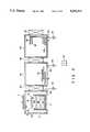
- a plasma etching apparatus 1comprises a process chamber 4 constituted by an inner cylinder 2 and an outer cylinder 3 which consist of a material such as aluminum.
- the inner cylinder 2is constituted by a cylindrical side portion 2a, a bottom portion 2b formed from the lower end of the side portion 2a to have a small interval at the upper portion of the bottom portion 2b, and a flange 2c formed at the outer peripheral portion of the lower end of the side portion 2a.
- the outer cylinder 3is constituted by a side portion 3a and a top portion 3b, and is mounted on the flange 2c to airtightly cover the inner cylinder 2.
- a gas supply path 5acapable of supplying a process gas such as an HF gas from a process gas source 5b into the process chamber 4 through a mass-flow controller (MFC) 5c is arranged at an upper portion of the side portion 3a.
- a gas exhaust path 6a connected to a vacuum pump 6bis arranged at an opposite lower portion of the side portion 3a, thereby evacuating the process chamber 4.
- a magnetic field generation membere.g., a permanent magnet 7, for forming a horizontal magnetic field on the surface of a target substrate, e.g., a semiconductor wafer W, is rotatably arranged above the top portion 3b of the outer cylinder 3.
- a magnetron dischargecan be generated in the process chamber 4.
- a stage 8 for placing and fixing the wafer Wis arranged in the process chamber 4.
- the stage 8is mounted on the bottom portion 2b in the inner cylinder 2 through a plurality of insulating members 9.
- An O-ring-like insulating member 10is interposed between the side surface of the stage 8 and the side portion 2a of the inner cylinder 2.
- the stage 8is held to be insulated from the inner cylinder 2 and the outer cylinder 3 which are grounded.
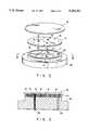
- the stage 8has three members 8a, 8b, and 8c stacked in the form of layers. As shown in FIG. 2, a groove 11 according to the present invention is formed in the flat placing surface of the susceptor 8a serving as the upper layer of the stage 8. A sheet-like electrostatic chuck 12 is fixed on the placing surface of the susceptor 8a with an adhesive.
- the electrostatic chuck 12as shown in FIG. 3, comprises a pair of dielectric films 13 and 14 which consist of a polyimide resin and are adhered to each other, and a chuck electrode 15 consisting of a thin conductive film such as a copper foil sealed between the films 13 and 14.
- the chuck electrode 15is connected to a DC power supply 17 through a lead having a switch 16.
- the electrostatic chuck 12is generally formed in the form of a circular flat sheet to have almost the same shape as that of the semiconductor wafer W.
- the electrostatic chuck 12is airtightly adhered to the susceptor 8a by an adhering means such as the adhesive so as to prevent leakage of a heat transfer gas supplied into the groove 11.
- the positive terminal of the DC power supply 17 having a voltage of, e.g., 2.0 kv,is connected to the chuck electrode 15 of the electrostatic chuck 12.
- the wafer Wis grounded through a plasma and the inner and outer cylinders 2 and 3. In this manner, polarization is caused in the upper dielectric film 13 of the electrostatic chuck 12, and the semiconductor wafer W is attracted and held on the electrostatic chuck 12 by Coulomb's force generated between the electrostatic chuck 12 and the semiconductor wafer W.
- a plurality of through holes 18are formed in the electrostatic chuck 12 to vertically extend through it. All the through holes 18, as shown in FIG. 2, are formed along the groove 11 formed in the placing surface of the susceptor 8a, and are positioned above the groove.
- the opening of a path 20 for supplying a heat transfer gasis positioned at the groove 11.
- the path 20is connected to a heat transfer gas source 21 for an inert gas such as He or N 2 , and the heat transfer gas is supplied onto the electrostatic chuck 12 through the path 20.
- the heat transfer gasis supplied, through the through holes 18, into an interstice BI between the electrostatic chuck 12 and the wafer W.
- an inert gassuch as He, N 2 , Ne, Ar, Kr, Xe, or Rn can be used.
- an inert gassuch as He, N 2 , Ne, Ar, Kr, Xe, or Rn
- an inert gasnot only an inert gas but also any gas, which can transfer cold with a minimum heat loss and does not easily react with a process gas in the process chamber 4 even if leakage occurs, can be used as the heat transfer gas. If necessary, the reaction in the process chamber 4 may be positively promoted by the heat transfer gas.
- a temperature adjustment membere.g., a heater 22, for adjusting the temperature of the wafer W is arranged in the heater fixing frame 8b serving as the intermediate layer of the stage 8.
- the heater 22is connected to a heater controller (not shown) to control the temperature of the susceptor 8a in accordance with a signal from a temperature monitor (not shown) for monitoring the temperature of the susceptor 8a or the heater fixing frame 8b.
- the temperature control of the susceptor 8ais disclosed in copending application Preliminary Ser. No. 08/154,451, the teachings of which are hereby incorporated by reference.
- the susceptor 8ais detachably fixed to the heater fixing frame 8b by connection members such as screws 23. Therefore, when the susceptor 8a is contaminated or damaged, only the susceptor 8a can be replaced with a new one independently of the heater fixing frame 8b connected to an RF power supply 24, and maintenance of the apparatus can be easily performed.
- a bore 26 for storing a coolant 25 such as liquid nitrogenis formed inside the cooling block 8c serving as the lower layer of the stage 8.
- the bore 26communicates with a liquid nitrogen source 29 by a pipe 27 through a valve 28.
- a liquid level monitor(not shown) is arranged in the bore 26, and the valve 28 is opened/closed in response to a signal from the liquid Level monitor, thereby controlling an amount of the coolant 25 supplied into the bore 26.
- the bottom surface of the bore 26is formed to be porous so as to be able cause nuclear boiling of the liquid nitrogen. Therefore, the temperature difference between the liquid nitrogen inside the cooling block 8c and the cooling block 8c can be kept at about 1° C.
- the insulating member 10such as an O-ring is interposed between the side wall of the susceptor 8a and the inner surface of the side portion 2a of the inner cylinder 2. Therefore, a process gas supplied into the process chamber does not reach a level lower than that of the susceptor 8a, so that the heater fixing frame 8b and the cooling block 8c are prevented from being contaminated.
- the stage 8is insulated by the insulating members 9 and 10 from the inner cylinder 2 and the outer cylinder 3 constituting the process chamber 4 so as to constitute a cathode coupling having the same electric polarity.
- the RF power supply 24is connected to the heater fixing frame 8b through a matching device 30. In this manner, the susceptor 8a and the grounded outer cylinder 3 constitute counter electrodes.
- a lower space 31 and a side space 32 which communicate with each otherare formed by the insulating members 9 and 10 between the stage 8 and the inner cylinder 2.
- the spaces 31 and 32can be evacuated by a vacuum pump 33b through an exhaust path 33a.
- Gaps 34 and 35are formed between the susceptor 8a and the heater fixing frame 8b and between the heater fixing frame 8b and the cooling block 8c, respectively.
- the gaps 34 and 35are airtightly constituted by seal members 36 and 37, e.g., O-rings.
- a heat transfer gas supplied from a gas source 39 through a path 38can be sealed in the gaps 34 and 35.
- Each of the gaps 34 and 35is formed to have a size of 1 to 100 ⁇ m, more preferably, about 50 ⁇ m.
- the same gas as the heat transfer gas supplied between the electrostatic chuck 12 and the lower surface of the semiconductor wafer Wcan be used. That is, an inert gas such as He, N 2 , Ne, Ar, Kr, Xe, or Rn can be used. Not only an inert gas but also any gas, which can transfer cold with a minimum heat loss and does not easily react with a process gas in the process chamber 4 even if leakage occurs, can be used as the heat transfer gas.
- the heat transfer gas from the gas source 21is temporarily supplied into the groove 11 formed in the upper surface of the susceptor 8a.
- the heat transfer gasis supplied at a uniform gas pressure from the groove 11 into the interstice BI between the electrostatic chuck 12 and the wafer W through the through holes 18 formed in the electrostatic chuck 12.
- the interstice BIis not sealed by the seal members 36 and 37 unlike the gaps 34 and 35.
- a heat transfer gas having a pressure of less than 20 Torrcan be sealed in the interstice BI by the Coulomb's force.
- Three vertically extending through holes 41are formed in the stage 8 and the electrostatic chuck 12.
- Vertically movable pins 42consisting of a conductive material is arranged in the through holes 41, respectively.
- the lower end portion of each of the three pins 42extends through the bottom portion 2b of the inner casing 2, and is mounted on a support plate 43 consisting of an insulating material under the bottom portion 2b.
- the pins 42can be selectively grounded through a line having a switch 48.
- the support plate 43is fixed on an output reciprocating rod 46 of a driving member 45. Therefore, the three pins 42 are vertically moved at once by the driving member 45 to assist a transfer arm 52 shown in FIG. 4 in loading/unloading the wafer W.
- the three vertically movable pins 42are surrounded by a bellows 47 between the support plate 43 and the bottom portion 2b of the inner casing 2.
- the support plate 43, the bottom portion 2b, and the bellows 47form an airtightly sealed space.
- Each of the pins 42is airtightly surrounded by the insulating seal rings 36 and 37 and an insulating seal pipe 44. Therefore, airtight communication can be performed from the top portion of each of the through holes 41 to the space surrounded by the bellows 47 on the support plate 43.
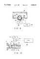
- An ionizer 71 for supplying an ionized gas into the interstice BI between the wafer W and the electrostatic chuck 12is connected to the path 20 for the heat transfer gas.
- the ionized gasis used to reduce residual charges left on the semiconductor wafer W and the electrostatic chuck 12 after the chuck electrode 15 is disconnected from the DC power supply 17.
- the ionizer 71is connected to the gas source 21 through a valve 72 such as an air-operated valve for starting or stopping supply of the heat transfer gas and a MFC 73 for controlling the supply amount of heat transfer gas.
- the ionizer 71comprises an ultraviolet lamp 80 having a glass window 81 formed at its distal end portion and airtightly arranged in the path 20.
- a power supply 82is connected to the ultraviolet lamp 80 through an electromagnetic switch 83.
- the switch 83is turned on or off in response to a control signal from a controller 84 of the apparatus.
- the electromagnetic switch 83When the electromagnetic switch 83 is turned on in response to the control signal from the controller 84, the ultraviolet lamp 80 is turned on to generate an ultraviolet beam, and the heat transfer gas in the path 20 is ionized with this ultraviolet beam.
- the ionized heat transfer gase.g., positively or negatively charged He, flows downstream in the path 20.
- an inert gassuch as He, N 2 , Ne, Ar, Kr, Xe, or Rn can be used.
- an exclusive gas source 74such as an N 2 source may be arranged independently of the heat transfer gas source 21 as another gas source.
- N 2is ionized to N 2 + and N 2 - by the ionizer 71, and N 2 + and N 2 - flow downstream in the path 20.
- a load lock chamber 51is connected to the outer cylinder 3 of the process chamber 4 of the magnetron plasma etching apparatus 1 according to the present invention through an openable gate 50.
- the transfer arm 52e.g., an aluminum convey arm, which is subjected to anti-electrostatic treatment by coating a conductive Teflon material, is arranged in the load lock chamber 51.
- An exhaust pipe 53is connected to an exhaust port formed in the bottom of the load lock chamber 51.
- a vacuum pump 55is connected to the exhaust pipe 53 through a vacuum exhaust valve 54 to be able to evacuate the load lock chamber 51.
- a cassette chamber 57is connected to a side wall of the load lock chamber 51 through an openable gate 56.
- a stage 59 for placing a cassette 58is arranged in the cassette chamber 57.
- the cassette 58can store 25 semiconductor wafers W serving as target substrates.
- An exhaust pipe 60is connected to an exhaust port formed in the bottom of the cassette chamber 57.
- the vacuum pump 55is connected to the exhaust pipe 60 through a vacuum exhaust valve 61 to be able to evacuate the cassette chamber 57.
- the other side wall of the cassette chamber 57communicates with the atmospheric air through an openable gate 62.
- the gate 62 arranged between the cassette chamber 57 and the atmospheric airis opened, the cassette 58 storing the wafers W is placed on the stage 59 of the cassette chamber 57 by a convey robot (not shown), and the gate 62 is closed.
- the vacuum exhaust valve 61 connected to the cassette chamber 57is opened, and the cassette chamber 57 is exhausted by the vacuum pump 55 to a low-pressure atmosphere, e.g., 10 -1 Tort.
- the gate 56 between the load lock chamber 51 and the cassette chamber 57is opened, and one of the wafers W is picked by the transfer arm 52 from the cassette 58 placed in the cassette chamber 57.
- the wafer Wis transferred into the load lock chamber 51 by the transfer arm 52, and the gate 56 is closed.
- the exhaust pipe 53 connected to the load lock chamber 51is opened, and the load lock chamber 51 is exhausted by the vacuum pump 55 to a low-pressure atmosphere, e.g., 10 -3 Torr.
- a process gas from the gas source 39is sealed in the gaps 34 and 35.
- Thermal energy, i.e., cold, of the coolant 25is transferred to the susceptor 8a to cool the susceptor 8a to a predetermined temperature.
- the gate 50 between the load lock chamber 51 and the process chamber 4is opened, and the wafer W is transferred into the process chamber 4 by the transfer arm 52.
- the wafer Wis placed on the stage 8, and the gate 50 is closed.
- the vertically movable pins 42are grounded, and the chuck electrode 15 is connected to the DC power supply 17.
- the lower surface of the wafer W grounded through the pins 42is negatively charged, and the upper surface of the dielectric film 13 of the electrostatic chuck 12 is positively charged.
- an electrostatic attractive forceis generated between the wafer W and the electrostatic chuck 12, and the wafer W is attracted and held on the stage 8.
- a heat transfer gas whose pressure is adjusted to a predetermined pressureis supplied into the interstice BI between the electrostatic chuck 12 and the wafer W. Cold or thermal energy from the coolant 25 is efficiently transferred to the wafer W by the heat transfer gas to cool the wafer W to an appropriate temperature.
- the process chamber 4is exhausted by the vacuum pump 55 to a low-pressure atmosphere, e.g., 10 -5 Torr, in advance.
- a process gase.g., an HF gas, is supplied from the gas supply path 5a into the process chamber 4.
- RF poweris applied from the RF power supply 24 to the heater fixing frame 8b, the process gas is made into a plasma, and RIE type plasma etching can be performed.
- the permanent magnet 7 arranged above the process chamber 4is rotated to form a magnetic field parallel to the surface of the wafer W near the wafer W. In this manner, ions can be directed perpendicularly to the wafer W, and etching having a high anisotropy can be achieved.
- the RF power supply 24is disconnected, and the supply of the process gas is stopped so as to stop generation of the plasma.
- an inert gassuch as nitrogen is supplied into the process chamber 4 to substitute the process gas or reaction products in the process chamber 4, while the process chamber 4 is exhausted by the vacuum pump 55.
- the chuck electrode 15is disconnected from the DC power supply 17, and the wafer waits for being transferred.
- an He gas from the gas source 21 or an inert gas, e.g., an N 2 gas, from the gas source 74is ionized by the ionizer 71, and the ionized gas is supplied onto the lower surface of the wafer W on the electrostatic chuck 12 through the path 20. That is, the UV lamp 80 shown in FIG. 9 is turned on, and He or N 2 is ionized by an ultraviolet beam.
- N 2 + and N 2 - generated by ionizing N 2are supplied between the wafer W and the electrostatic chuck 12 through the path 20 while a flow rate of N 2 + and N 2 - is adjusted, positive charges attracted by the wafer W and negative charges attracted by the electrostatic chuck 12 are neutralized by the N 2 + and N 2 - gases, respectively, thereby performing a charge-removing operation of the wafer W and the electrostatic chuck 12.
- a charge-removing timeis determined as follows. That is, assuming that the distance between the ionizer 71 and the semiconductor wafer W is set to be about 25 cm and that a potential of 3 kv is left, positive charges can be removed within 3 seconds or less, and negative charges can be removed within 10 seconds or less to a potential of about 0.3 kv or less. As the distance between the ionizer 71 and the wafer W is shorter, the charge-removing time can be shortened. The distance is preferably set to be 20 cm or less.
- the time required for performing a charge-removing operation of the wafer W and the electrostatic chuck 12is shorter in an atmospheric pressure atmosphere than in a low-pressure atmosphere.
- the charge-removing time at a pressure of 1 ⁇ 10 -2 Torr or lesscan be shortened by 1.5 times or more the charge-removing time obtained at the atmospheric pressure.
- the gate 50 arranged on the side of the process chamber 4is opened.
- the wafer Wis lifted from the electrostatic chuck 12 by the pins 42.
- the transfer arm 52moves to the position of the wafer W to receive the wafer W from the pins 42.
- the gate 50is closed.
- the wafer Wis heated by the heater to a room temperature, e.g., 18° C. Thereafter, the wafer W is unloaded from the lead lock chamber 51 into the air through the cassette chamber 57.
- the groove 11has a uniform depth and is formed all over the surface of the susceptor 8a as shown in FIG. 2.
- the groove 11has a width of 1.2 mm and a depth of 1.5 mm.
- the groove 11may be constituted to have a width and a depth at a ratio of 1:2.
- the width of the groove 11preferably falls within a range of 0.5 to 3 mm. If the width is smaller than this range, circulation of the heat transfer gas may be disturbed; if the width is larger than the range, a polyimide resin film of the electrostatic chuck 12 is expanded by supplying the heat transfer gas, and it may not be able to preferably hold and attract the wafer W.
- the depth of the groove 11is preferably set to be 0.5 mm or more. If the depth is smaller than this range, an adhesive for adhering the electrostatic chuck 12 may clog up the groove 11.
- the flat mounting surface of the susceptor 8ahas a diameter substantially equal to that of the electrostatic chuck 12. That is, in this embodiment, the area of the mounting surface is substantially equal to the area of the lower surface of the electrostatic chuck 12.
- the total area of the groove 11 in the plan view, i.e., the opening area of the groove 11,is preferably set to be 15% or less than 15% of the area of the lower surface of the electrostatic chuck 12. If the area is larger than the range, the attraction force obtained may be insufficient.
- An endless loop groove or annular groove portion 19is formed along the peripheral edge of the mounting surface of the susceptor 8a.
- the endless loop groove portion 19functions as a reservoir for the heat transfer gas, and has a role of assuring good heat transfer properties at the peripheral portion of the wafer W where the heat transfer gas easily escapes into the process chamber 4. Therefore, the endless loop groove portion 19 has a sectional area of 2 to 4 mm 2 , and is preferably formed on the mounting surface of the susceptor 8a to correspond to a region distant from the peripheral edge of the electrostatic chuck 12 by smaller than 5 mm.
- the through holes 41 for the vertically movable pins 42are arranged to communicate with the groove 11. In this manner, the heat transfer gas can be supplied into the through holes 41.
- the through holes 41can exhaust the gas through the groove 11 when an initial low pressure is set before the wafer W is not placed. Since the three through holes 41 communicate with each other through an airtight space surrounded by the bellows 47, when at least one of the through holes 41 communicates with the groove 11, all the through holes 41 communicate with the groove 11.
- the heat conductivity in the through holes 41can be increased by supplying therein the heat transfer gas. If necessary, the heat transfer gas can be supplied into the through holes 41 by connecting the line for the heat transfer gas to the support plate 43.
- the electrostatic chuck 12is adhered to the entire mounting surface of the susceptor 8a except for a portion where the groove 11 is formed.
- the through holes 18 formed in the electrostatic chuck 12are almost uniformly distributed on the entire surface of the electrostatic chuck 12, and arranged to communicate with the groove 11.
- the diameter of each of the through holes 18falls within a range of 0.6 to 1.5 mm.
- the 60 to 70 through holes 18are formed in an electrostatic chuck for a 6" wafer, and the 100 to 120 through holes are formed in an electrostatic chuck for an 8" wafer.
- a heat transfer gas having a pressure of 5 to 15 Tort, preferably, 10 Torris supplied from the heat transfer gas source 21 into the groove 11 through the path 20.
- the heat transfer gasis supplied from the groove 11 into the interstice BI between the electrostatic chuck 12 and the wafer W through the through holes 18 of the electrostatic chuck 12.
- the DC power supply 17is turned off while the heat transfer gas is left in the interstice BI, the wafer W may be jumped from the susceptor 8a due to the pressure of the residual gas. Therefore, after the heat transfer gas is evacuated from the interstice BI between the electrostatic chuck 12 and the wafer W, the DC power supply 17 is turned off.
- FIGS. 5 to 7show modifications of the stage according to the present invention.
- the same reference numerals as in FIGS. 5 to 7denote the same parts in FIGS. 1 to 3, and a description thereof will be omitted.
- each groove 11is constituted by large groove elements 11a having a depth of 2 mm and a width of 2 mm and small groove elements 11b each having a depth of 0.5 mm and a width of 1 mm.
- Each annular groove portion 19is formed as the large groove 11a. Referring to FIGS. 5 to 7, each of the large groove elements 11a is indicated by a double line, and each of the small groove elements 11a is indicated by a single line.
- the heat transfer gas supplied from the path 20can be efficiently, rapidly supplied onto the entire surface of a susceptor by the large groove elements 11a, and a heat conduction medium can be distributed to fine portions of the upper surface of the susceptor by the small groove elements 11b.
- the heat transfer gascan be efficiently, rapidly distributed to the lower surface of the electrostatic chuck 12 at a uniform pressure.
- the sectional area of each of the large groove elements 11apreferably falls within a range of 2 to 4 mm 2
- the sectional area of each of the small groove elements 11bpreferably falls within a range of 0.5 to 1.0 mm 2 .
- an annular groove portion 19 and a groove portion for connecting the annular groove portion 19 to the opening of a path 20are constituted by the large groove elements 11a, and the small groove elements 11b are formed in the form of veins.
- the annular groove portion 19 and a groove portion for connecting the annular groove portion 19 and the opening of the path 20are constituted by the large groove elements 11a, and the small groove elements 11b are formed in a matrix form.
- the large groove element 11ais coaxially arranged inside the annular groove portion 19, and the small groove elements 11a are radially arranged.
- the shape of the groove 11is not limited to the shapes of the modifications shown in FIGS.
- any groove which can efficiently, rapidly distribute the heat transfer gas onto the surface of the susceptor 8a, i.e., the entire lower surface of the electrostatic chuck 12can be used as the groove 11.
- Various modificationscan be constituted without departing from the spirit and scope of the invention.
- FIG. 8shows still another modification of a stage according to the present invention.
- the same reference numerals as in FIGS. 1 to 3denote the same parts in FIG. 8, and a description thereof will be omitted.
- a reservoir 65is formed midway along a path 20. In this manner, the pressure of a heat transfer gas supplied from a gas source 21 is uniformed, and a supply speed can be increased.
- a seam 66 for forming the reservoir 65 in a susceptor 8ais sealed by a means such as welding not to cause leakage of the heat transfer gas.
- FIG. 10shows an ionizer 111 which can be arranged in the gas supply path 5a and is used to perform a charge-removing operation.
- the ionizer 111comprises discharge rods 112 and 113, independently coated with quartz glass members 114 and 115, for generating a corona discharge.
- the distal end portions of the quartz glass members 114 and 115are buried in the supply path 5a, and the peripheral portions of the distal end portions of the quartz glass members 114 and 115 are airtightly connected to the supply tube 5a.
- the discharge rods 112 and 113extend through an insulator 116, e.g., a ceramic material, for preventing an electric shock, and are connected to a power supply 117 through electromagnetic switches 118, respectively.
- Each of the electromagnetic switches 118is turned on/off in response to a control signal from a controller 84.
- Charges left on the lower surface of the wafer W and the surface of the electrostatic chuck 12are removed by the ionizer 111 after generation of a plasma is stopped and a DC power supply 17 for the chuck electrode 15 is disconnected.
- an inert gassuch as N 2 flows in the gas supply path 5a, and this gas is ionized to N 2 + and N 2 - by the ionizer 111.
- An ionization atmosphere of N 2 + and N 2 -is formed on the wafer W.
- This charge-removing operationmay be performed in place of the charge-removing operation of the first embodiment in which a charge-removing operation is performed through the path 20, or both the charge-removing operation of this embodiment and the charge-removing operation of the first embodiment may be simultaneously performed.
- FIG. 11shows an ionizer 150 which can be arranged on the side wall of the process chamber 4 and is used to perform a charge-removing operation.
- the ionizer 150comprises discharge rods 151 and 152, covered with a quartz glass member 153, for generating a corona discharge.
- the quartz glass memberis airtightly connected to an insulator, e.g., a ceramic base 154.
- the distal end portion of an extendible member 155e.g., a bellows, is airtightly connected to the peripheral portion of the base 154.
- the proximal end of the extendible member 155is airtightly connected to the inner peripheral portion of a hole portion 158 formed in the side wall of the process chamber 4.
- the extendible member 155includes a horizontally movable portion 157 which is driven by a driving member 156, e.g., a motor or an air cylinder.
- the distal end portion of the movable portion 157is connected to the base 154. Therefore, the extendible member 155 can move the ionizer 150 from a position (when charges on the wafer W are removed) above the wafer W to a position (when the wafer W is subjected to plasma processing) where the ionizer 150 is withdrawn from the position above the wafer W.
- Wires 160 and 161 for supplying a voltage to the discharge rods 151 and 152are arranged in the extendible member 155 and connected to the power supply 117 through electromagnetic switches 162 and 163, respectively.
- the electromagnetic switches 162 and 163are turned on/off in response to a control signal from an apparatus controller 84 for controlling the apparatus.
- the ionizer 150extends to the position above the wafer W.
- An inert gas such as N 2flows in a gas supply path 5a, and this gas is ionized to N 2 + and N 2hu - by the ionizer 150 to form an ionization atmosphere of N 2 + and N 2 - on the wafer W.
- This charge-removing operationmay be performed in place of the charge-removing operation of the first embodiment in which a charge-removing operation is performed through the path 20, or both the charge-removing operation of this embodiment and the charge-removing operation of the first embodiment may be simultaneously performed.
- FIG. 12shows an ionizer 180 which can be arranged in an auxiliary chamber connected to the process chamber 4 and is used to perform a charge-removing operation.
- an opening 181is formed in the side wall of the process chamber 4, and is opened/closed by a gate 182.
- An O-ring arranged in the side wall of the process chamber 4is pressed by the gate 182 so as to airtightly close the process chamber 4.
- An auxiliary chamber 183is connected to the opening 181 through the gate 182.
- a transfer arm 185is arranged in the auxiliary chamber 183, and an ultraviolet lamp 184 is supported on the transfer arm 185.
- the ultraviolet lamp 184can be horizontally moved above the wafer W on a stage 8 by the transfer arm 185.
- the ultraviolet lamp 184is ON/OFF-controlled by a controller (not shown).
- the transfer arm 185extends to position the lamp 184 in the process chamber 4.
- An inert gas such as N 2flows in a gas supply path 5a, and this gas is ionized to N 2 + and N 2 - by the ionizer 180 to form an ionization atmosphere of N 2 + and N 2 - on the wafer W.
- This charge-removing operationmay be performed in place of the charge-removing operation of the first embodiment in which a charge-removing operation is performed through the path 20, or both the charge-removing operation of this embodiment and the charge-removing operation of the first embodiment may be simultaneously performed.
- a charge-removing operationmay be performed while the wafer W is lifted by vertically movable pins 42 which are grounded.
- a charge-removing operation of the lower surface of the wafer Wis mainly performed through the pins 42, and a charge-removing operation of the upper surface of the electrostatic chuck 12 is performed by each of the ionizers. Only the charge-removing operation of the upper surface of the electrostatic chuck 12 may be performed by each of the ionizers after the wafer W is transferred into a load lock chamber 51 (see FIG. 4).
- a load lock chamber 51see FIG. 4
- an ionization atmospheremay be formed by ionizing a residual gas in the process chamber 4 without supplying an inert gas through the gas supply path 5a. Modifications of such a charge-removing operation will be described below using the ionizer 180 shown in FIG. 12 as an example.
- the gate 182is opened, and a transfer arm 185 extends to move the ultraviolet lamp 184 from the auxiliary chamber 183 into a process chamber 4.
- the ultraviolet lamp 184is turned on and moved above the electrostatic chuck 12 so as to cover the entire area of the electrostatic chuck 12.
- movements of the lamp 184a spiral motion shown in FIG. 13, a reciprocating motion shown in FIG. 14, and a concentrically circular motion shown in FIG. 15 are considered.
- the residual gas, e.g., a CO gas, in the process chamber 4is ionized to CO + and CO - with an ultraviolet beam radiated from the lamp 184.
- An ionization atmosphere formed by the ionized gascauses charges left on the upper surface of the electrostatic chuck 12 to be removed through the ionization atmosphere and the inner and outer cylinders 2 and 3.
- a charge-removing timeis determined as follows. That is, assuming that the distance between the lamp 184 and the wafer W is set to be about 25 cm and that a potential of 3 kv is left, positive charges can be removed within 3 seconds or less, and negative charges can be removed within 10 seconds or less to a potential of about 0.3 kV or less. As the distance between the lamp 184 and the wafer W is shorter, the charge-removing time can be shortened. The distance is preferably set to be 20 cm or less.
- the present inventionis especially suitable for the stage of a plasma processing apparatus in which a heat transfer gas is required for controlling the temperature of a target substrate in a vacuum atmosphere.
- the present inventioncan be applied to not only the stage of the plasma processing apparatus but also a stage used in the air.
- a meanssuch as a vertically movable pin of the apparatus shown in FIG. 1, for applying a potential different from that of a chuck electrode, may be arranged.
- a plasma processing apparatusin addition to a plasma etching apparatus, a plasma ashing apparatus and a plasma CVD apparatus can be used.
- a target substratein addition to a semiconductor wafer, a substrate for an LCD can be used.
Landscapes
- Chemical & Material Sciences (AREA)
- Engineering & Computer Science (AREA)
- Mechanical Engineering (AREA)
- General Chemical & Material Sciences (AREA)
- Organic Chemistry (AREA)
- Metallurgy (AREA)
- Materials Engineering (AREA)
- Chemical Kinetics & Catalysis (AREA)
- Microelectronics & Electronic Packaging (AREA)
- Condensed Matter Physics & Semiconductors (AREA)
- Power Engineering (AREA)
- General Physics & Mathematics (AREA)
- Physics & Mathematics (AREA)
- Computer Hardware Design (AREA)
- Manufacturing & Machinery (AREA)
- Drying Of Semiconductors (AREA)
- Container, Conveyance, Adherence, Positioning, Of Wafer (AREA)
Abstract
Description
Claims (20)
Applications Claiming Priority (6)
| Application Number | Priority Date | Filing Date | Title |
|---|---|---|---|
| JP35470992AJP3021217B2 (en) | 1992-12-17 | 1992-12-17 | Electrostatic chuck |
| JP35524092AJPH06188305A (en) | 1992-12-17 | 1992-12-17 | Apparatus and method for separation of body to be attracted as well as plasma processing apparatus |
| JP4-354709 | 1992-12-17 | ||
| JP4-355240 | 1992-12-17 | ||
| JP5-089239 | 1993-03-24 | ||
| JP8923993AJPH06275546A (en) | 1993-03-24 | 1993-03-24 | Plasma treating device |
Publications (1)
| Publication Number | Publication Date |
|---|---|
| US5382311Atrue US5382311A (en) | 1995-01-17 |
Family
ID=27306072
Family Applications (1)
| Application Number | Title | Priority Date | Filing Date |
|---|---|---|---|
| US08/168,367Expired - LifetimeUS5382311A (en) | 1992-12-17 | 1993-12-17 | Stage having electrostatic chuck and plasma processing apparatus using same |
Country Status (2)
| Country | Link |
|---|---|
| US (1) | US5382311A (en) |
| KR (1) | KR100238629B1 (en) |
Cited By (699)
| Publication number | Priority date | Publication date | Assignee | Title |
|---|---|---|---|---|
| EP0700078A1 (en)* | 1994-09-01 | 1996-03-06 | Applied Materials, Inc. | Support members for semiconductor wafers in a processing environment |
| US5507874A (en)* | 1994-06-03 | 1996-04-16 | Applied Materials, Inc. | Method of cleaning of an electrostatic chuck in plasma reactors |
| US5532903A (en)* | 1995-05-03 | 1996-07-02 | International Business Machines Corporation | Membrane electrostatic chuck |
| US5539609A (en)* | 1992-12-02 | 1996-07-23 | Applied Materials, Inc. | Electrostatic chuck usable in high density plasma |
| US5547539A (en)* | 1993-12-22 | 1996-08-20 | Tokyo Electron Limited | Plasma processing apparatus and method |
| US5552955A (en)* | 1994-02-03 | 1996-09-03 | Anelva Corporation | Substrate removal method and mechanism for effecting the method |
| US5573981A (en)* | 1993-09-21 | 1996-11-12 | Sony Corporation | Method of removing residual charges of an electrostatic chuck used in a layer deposition process |
| US5578164A (en)* | 1993-12-24 | 1996-11-26 | Tokyo Electron Limited | Plasma processing apparatus and method |
| EP0755066A1 (en)* | 1995-07-18 | 1997-01-22 | Applied Materials, Inc. | Electrostatic chuck |
| US5609720A (en)* | 1995-09-29 | 1997-03-11 | Lam Research Corporation | Thermal control of semiconductor wafer during reactive ion etching |
| US5634266A (en)* | 1994-02-28 | 1997-06-03 | Applied Materials Inc. | Method of making a dielectric chuck |
| EP0777262A1 (en)* | 1995-11-28 | 1997-06-04 | Applied Materials, Inc. | Wafer heater assembly |
| US5656093A (en)* | 1996-03-08 | 1997-08-12 | Applied Materials, Inc. | Wafer spacing mask for a substrate support chuck and method of fabricating same |
| EP0790641A1 (en)* | 1996-02-16 | 1997-08-20 | Novellus Systems, Inc. | Wafer cooling device |
| US5665166A (en)* | 1993-01-29 | 1997-09-09 | Tokyo Electron Limited | Plasma processing apparatus |
| US5665167A (en)* | 1993-02-16 | 1997-09-09 | Tokyo Electron Kabushiki Kaisha | Plasma treatment apparatus having a workpiece-side electrode grounding circuit |
| US5671119A (en)* | 1996-03-22 | 1997-09-23 | Taiwan Semiconductor Manufacturing Company, Ltd. | Process for cleaning an electrostatic chuck of a plasma etching apparatus |
| US5697427A (en)* | 1995-12-22 | 1997-12-16 | Applied Materials, Inc. | Apparatus and method for cooling a substrate |
| US5708556A (en)* | 1995-07-10 | 1998-01-13 | Watkins Johnson Company | Electrostatic chuck assembly |
| US5729423A (en)* | 1994-01-31 | 1998-03-17 | Applied Materials, Inc. | Puncture resistant electrostatic chuck |
| US5736818A (en)* | 1996-03-15 | 1998-04-07 | Board Of Trustees Operating Michigan State University | Resonant radiofrequency wave plasma generating apparatus with improved stage |
| US5745331A (en)* | 1994-01-31 | 1998-04-28 | Applied Materials, Inc. | Electrostatic chuck with conformal insulator film |
| US5746928A (en)* | 1996-06-03 | 1998-05-05 | Taiwan Semiconductor Manufacturing Company Ltd | Process for cleaning an electrostatic chuck of a plasma etching apparatus |
| US5748435A (en)* | 1996-12-30 | 1998-05-05 | Applied Materials, Inc. | Apparatus for controlling backside gas pressure beneath a semiconductor wafer |
| US5761023A (en)* | 1996-04-25 | 1998-06-02 | Applied Materials, Inc. | Substrate support with pressure zones having reduced contact area and temperature feedback |
| US5800618A (en)* | 1992-11-12 | 1998-09-01 | Ngk Insulators, Ltd. | Plasma-generating electrode device, an electrode-embedded article, and a method of manufacturing thereof |
| US5801915A (en)* | 1994-01-31 | 1998-09-01 | Applied Materials, Inc. | Electrostatic chuck having a unidirectionally conducting coupler layer |
| US5811021A (en)* | 1995-02-28 | 1998-09-22 | Hughes Electronics Corporation | Plasma assisted chemical transport method and apparatus |
| US5815366A (en)* | 1994-12-28 | 1998-09-29 | Sumitomo Metal Industries, Ltd. | Electrostatic chuck and the method of operating the same |
| US5835334A (en)* | 1996-09-30 | 1998-11-10 | Lam Research | Variable high temperature chuck for high density plasma chemical vapor deposition |
| US5847918A (en)* | 1995-09-29 | 1998-12-08 | Lam Research Corporation | Electrostatic clamping method and apparatus for dielectric workpieces in vacuum processors |
| US5885469A (en)* | 1996-11-05 | 1999-03-23 | Applied Materials, Inc. | Topographical structure of an electrostatic chuck and method of fabricating same |
| US5885353A (en)* | 1996-06-21 | 1999-03-23 | Micron Technology, Inc. | Thermal conditioning apparatus |
| WO1999016926A1 (en)* | 1997-09-26 | 1999-04-08 | Cvc Products, Inc. | Two-stage sealing system for thermally conductive chuck |
| US5906684A (en)* | 1993-09-16 | 1999-05-25 | Hitachi, Ltd. | Method of holding substrate and substrate holding system |
| US5948986A (en)* | 1997-12-26 | 1999-09-07 | Applied Materials, Inc. | Monitoring of wafer presence and position in semiconductor processing operations |
| US5950723A (en)* | 1995-11-17 | 1999-09-14 | Cvc Products, Inc. | Method of regulating substrate temperature in a low pressure environment |
| US6002572A (en)* | 1997-03-25 | 1999-12-14 | Tokyo Electron Limited | Processing apparatus and a processing method |
| US6008978A (en)* | 1997-05-07 | 1999-12-28 | Tokyo Electron Limited | Discharging method and processing apparatus having discharging function |
| WO2000019775A1 (en)* | 1998-09-25 | 2000-04-06 | Aehr Test Systems | Wafer level burn-in and test thermal chuck and method |
| US6053982A (en)* | 1995-09-01 | 2000-04-25 | Asm America, Inc. | Wafer support system |
| US6074512A (en)* | 1991-06-27 | 2000-06-13 | Applied Materials, Inc. | Inductively coupled RF plasma reactor having an overhead solenoidal antenna and modular confinement magnet liners |
| US6073576A (en)* | 1997-11-25 | 2000-06-13 | Cvc Products, Inc. | Substrate edge seal and clamp for low-pressure processing equipment |
| US6080272A (en)* | 1998-05-08 | 2000-06-27 | Micron Technology, Inc. | Method and apparatus for plasma etching a wafer |
| US6083569A (en)* | 1996-10-25 | 2000-07-04 | Applied Materials, Inc. | Discharging a wafer after a plasma process for dielectric deposition |
| US6104595A (en)* | 1998-04-06 | 2000-08-15 | Applied Materials, Inc. | Method and apparatus for discharging an electrostatic chuck |
| US6113702A (en)* | 1995-09-01 | 2000-09-05 | Asm America, Inc. | Wafer support system |
| WO2000019492A3 (en)* | 1998-09-30 | 2000-11-16 | Applied Materials Inc | Cathode assembly containing an electrostatic chuck for retaining a wafer in a semiconductor wafer processing system |
| US6181555B1 (en) | 1995-09-29 | 2001-01-30 | Intel Corporation | Cooling system for integrated circuit chips in a portable computer |
| US6257045B1 (en) | 1997-10-10 | 2001-07-10 | Applied Komatsu Technology, Inc. | Automated substrate processing systems and methods |
| US6278600B1 (en) | 1994-01-31 | 2001-08-21 | Applied Materials, Inc. | Electrostatic chuck with improved temperature control and puncture resistance |
| US6373679B1 (en) | 1999-07-02 | 2002-04-16 | Cypress Semiconductor Corp. | Electrostatic or mechanical chuck assembly conferring improved temperature uniformity onto workpieces held thereby, workpiece processing technology and/or apparatus containing the same, and method(s) for holding and/or processing a workpiece with the same |
| US6375750B1 (en) | 1995-07-10 | 2002-04-23 | Applied Materials, Inc. | Plasma enhanced chemical processing reactor and method |
| US6384383B2 (en)* | 1999-12-09 | 2002-05-07 | Shin-Etsu Chemical Co., Ltd. | Ceramic heating jig |
| US6394797B1 (en) | 1997-04-02 | 2002-05-28 | Hitachi, Ltd. | Substrate temperature control system and method for controlling temperature of substrate |
| US6406545B2 (en) | 1999-07-27 | 2002-06-18 | Kabushiki Kaisha Toshiba | Semiconductor workpiece processing apparatus and method |
| US6436739B1 (en)* | 2000-04-27 | 2002-08-20 | The Regents Of The University Of California | Thick adherent dielectric films on plastic substrates and method for depositing same |
| US6456480B1 (en) | 1997-03-25 | 2002-09-24 | Tokyo Electron Limited | Processing apparatus and a processing method |
| US6486070B1 (en)* | 2000-09-21 | 2002-11-26 | Lam Research Corporation | Ultra-high oxide to photoresist selective etch of high-aspect-ratio openings in a low-pressure, high-density plasma |
| US6490145B1 (en) | 2001-07-18 | 2002-12-03 | Applied Materials, Inc. | Substrate support pedestal |
| WO2002047120A3 (en)* | 2000-12-04 | 2002-12-27 | Applied Materials Inc | Cooling gas delivery system for a rotatable semiconductor substrate support assembly |
| US6500299B1 (en) | 1999-07-22 | 2002-12-31 | Applied Materials Inc. | Chamber having improved gas feed-through and method |
| US6506291B2 (en) | 2001-06-14 | 2003-01-14 | Applied Materials, Inc. | Substrate support with multilevel heat transfer mechanism |
| SG93851A1 (en)* | 1998-11-30 | 2003-01-21 | Kawasaki Microelectronics Inc | Method and apparatus for processing semiconductor substrates |
| US6513796B2 (en)* | 2001-02-23 | 2003-02-04 | International Business Machines Corporation | Wafer chuck having a removable insert |
| US20030033116A1 (en)* | 2001-08-07 | 2003-02-13 | Tokyo Electron Limited Of Tbs Broadcast Center | Method for characterizing the performance of an electrostatic chuck |
| US20030029610A1 (en)* | 1997-01-02 | 2003-02-13 | Cvc Products, Inc. | Thermally conductive chuck for vacuum processor |
| US6572814B2 (en) | 1998-09-08 | 2003-06-03 | Applied Materials Inc. | Method of fabricating a semiconductor wafer support chuck apparatus having small diameter gas distribution ports for distributing a heat transfer gas |
| US20030168174A1 (en)* | 2002-03-08 | 2003-09-11 | Foree Michael Todd | Gas cushion susceptor system |
| US6630053B2 (en)* | 2000-08-22 | 2003-10-07 | Asm Japan K.K. | Semiconductor processing module and apparatus |
| US6639783B1 (en) | 1998-09-08 | 2003-10-28 | Applied Materials, Inc. | Multi-layer ceramic electrostatic chuck with integrated channel |
| WO2003100849A1 (en)* | 2002-05-28 | 2003-12-04 | Tokyo Electron Limited | Semiconductor processor |
| US6660975B2 (en) | 2000-05-18 | 2003-12-09 | Matrix Integrated Systems, Inc. | Method for producing flat wafer chucks |
| EP0827187A3 (en)* | 1996-08-26 | 2004-01-07 | Applied Materials, Inc. | Method and apparatus for cooling a workpiece using an electrostatic chuck |
| US20040045813A1 (en)* | 2002-09-03 | 2004-03-11 | Seiichiro Kanno | Wafer processing apparatus, wafer stage, and wafer processing method |
| US6705394B1 (en) | 1999-10-29 | 2004-03-16 | Cvc Products, Inc. | Rapid cycle chuck for low-pressure processing |
| US6712019B2 (en)* | 1996-02-08 | 2004-03-30 | Canon Kabushiki Kaisha | Film forming apparatus having electrically insulated element that introduces power of 20-450MHz |
| US20040087168A1 (en)* | 1996-07-08 | 2004-05-06 | Granneman Ernst Hendrik August | Method and apparatus for supporting a semiconductor wafer during processing |
| US20040187787A1 (en)* | 2003-03-31 | 2004-09-30 | Dawson Keith E. | Substrate support having temperature controlled substrate support surface |
| US20040223286A1 (en)* | 2000-11-09 | 2004-11-11 | Samsung Electronics Co., Ltd. | Wafer stage including electrostatic chuck and method for dechucking wafer using the wafer stage |
| US20040261721A1 (en)* | 2003-06-30 | 2004-12-30 | Steger Robert J. | Substrate support having dynamic temperature control |
| US6844921B2 (en)* | 2001-11-20 | 2005-01-18 | Oki Electric Industry Co., Ltd. | Wafer holder |
| US20050012403A1 (en)* | 2003-07-15 | 2005-01-20 | Michael Binnard | Dual flow circulation system for a mover |
| US20050011456A1 (en)* | 2001-11-30 | 2005-01-20 | Tokyo Electron Limited | Processing apparatus and gas discharge suppressing member |
| US20050018169A1 (en)* | 2000-03-10 | 2005-01-27 | Canon Kabushiki Kaisha | Substrate holding device, semiconductor manufacturing apparatus and device manufacturing method |
| EP1205964A4 (en)* | 1999-06-21 | 2005-02-02 | Tokyo Electron Ltd | Plasma process device, electrode structure thereof, and stage structure |
| US20050040712A1 (en)* | 2003-08-21 | 2005-02-24 | Hazelton Andrew J. | Mover combination with two circulation flows |
| US20050051098A1 (en)* | 2003-09-05 | 2005-03-10 | Tooru Aramaki | Plasma processing apparatus |
| US20050067147A1 (en)* | 2003-09-02 | 2005-03-31 | Thayer John Gilbert | Loop thermosyphon for cooling semiconductors during burn-in testing |
| US20050067155A1 (en)* | 2003-09-02 | 2005-03-31 | Thayer John Gilbert | Heat pipe evaporator with porous valve |
| US20050068734A1 (en)* | 2003-09-02 | 2005-03-31 | Thayer John Gilbert | Heat pipe with chilled liquid condenser system for burn-in testing |
| US20050067146A1 (en)* | 2003-09-02 | 2005-03-31 | Thayer John Gilbert | Two phase cooling system method for burn-in testing |
| US20050087136A1 (en)* | 2003-10-08 | 2005-04-28 | Tokyo Electron Limited | Particle sticking prevention apparatus and plasma processing apparatus |
| US20050092438A1 (en)* | 2003-11-04 | 2005-05-05 | Hur Gwang H. | Flat panel display manufacturing apparatus |
| US20050092811A1 (en)* | 2002-03-20 | 2005-05-05 | Lee Sang S. | Bonding device for manufacturing liquid crystal display device |
| EP1304726A3 (en)* | 2001-10-18 | 2005-07-27 | Infineon Technologies AG | Device and method for receiving and for processing a thin wafer |
| US20050178335A1 (en)* | 2001-03-02 | 2005-08-18 | Tokyo Electron Limited | Method and apparatus for active temperature control of susceptors |
| US20050221552A1 (en)* | 2004-02-26 | 2005-10-06 | Applied Materials, Inc. | Substrate support for in-situ dry clean chamber for front end of line fabrication |
| US20050231886A1 (en)* | 2004-04-16 | 2005-10-20 | Innolux Display Corp. | Substrate attaching device and method |
| US20060051966A1 (en)* | 2004-02-26 | 2006-03-09 | Applied Materials, Inc. | In-situ chamber clean process to remove by-product deposits from chemical vapor etch chamber |
| US20060164632A1 (en)* | 2001-12-12 | 2006-07-27 | Tokyo Electron Limited | Method and apparatus for position-dependent optical metrology calibration |
| US20060204356A1 (en)* | 2005-03-08 | 2006-09-14 | Asm Japan K.K. | Semiconductor-manufacturing apparatus equipped with cooling stage and semiconductor-manufacturing method using same |
| US20060249254A1 (en)* | 1995-03-16 | 2006-11-09 | Saburo Kanai | Plasma processing apparatus and plasma processing method |
| US20060292896A1 (en)* | 2005-01-06 | 2006-12-28 | Hsien-Che Teng | Heater for heating a wafer and method for preventing contamination of the heater |
| US20070151673A1 (en)* | 2005-12-29 | 2007-07-05 | Lg.Philips Lcd Co., Ltd. | Substrate bonding apparatus for liquid crystal display panel |
| US20070169703A1 (en)* | 2006-01-23 | 2007-07-26 | Brent Elliot | Advanced ceramic heater for substrate processing |
| US20070217119A1 (en)* | 2006-03-17 | 2007-09-20 | David Johnson | Apparatus and Method for Carrying Substrates |
| US20070274020A1 (en)* | 2003-12-22 | 2007-11-29 | Adaptive Plasma Technology Corporation | Electrostatic Chuck And Chuck Base Having Cooling Path For Cooling Wafer |
| US20070283891A1 (en)* | 2006-03-29 | 2007-12-13 | Nobuyuki Okayama | Table for supporting substrate, and vacuum-processing equipment |
| US20080061032A1 (en)* | 2006-09-07 | 2008-03-13 | Applied Materials, Inc. | Electrostatic chuck cleaning during semiconductor substrate processing |
| US20080073563A1 (en)* | 2006-07-01 | 2008-03-27 | Nikon Corporation | Exposure apparatus that includes a phase change circulation system for movers |
| CN100397566C (en)* | 2005-12-02 | 2008-06-25 | 北京北方微电子基地设备工艺研究中心有限责任公司 | Silicon chip unloading process for reducing plasma damage |
| CN100399504C (en)* | 2005-12-02 | 2008-07-02 | 北京北方微电子基地设备工艺研究中心有限责任公司 | Silicon chip unloading process |
| US20080160210A1 (en)* | 2004-02-26 | 2008-07-03 | Haichun Yang | Passivation layer formation by plasma clean process to reduce native oxide growth |
| WO2008066841A3 (en)* | 2006-11-29 | 2008-08-28 | Edwards Vacuum Inc | Inductively heated trap |
| CN100429759C (en)* | 2005-06-06 | 2008-10-29 | 东京毅力科创株式会社 | Substrate supporting unit, and substrate temperature control apparatus and method |
| US20080279659A1 (en)* | 2007-05-07 | 2008-11-13 | Lintec Corporation | Transferring device and transferring method |
| US20080314320A1 (en)* | 2005-02-04 | 2008-12-25 | Component Re-Engineering Company, Inc. | Chamber Mount for High Temperature Application of AIN Heaters |
| US20090156015A1 (en)* | 2007-12-18 | 2009-06-18 | Asm Genitech Korea Ltd. | Deposition apparatus |
| US20090293809A1 (en)* | 2008-05-28 | 2009-12-03 | Sang-Bum Cho | Stage unit for supporting a substrate and apparatus for processing a substrate including the same |
| US20100000684A1 (en)* | 2008-07-03 | 2010-01-07 | Jong Yong Choi | Dry etching apparatus |
| US20100015558A1 (en)* | 2006-06-08 | 2010-01-21 | Datalase Ltd | Laser Marking |
| EP1811559A4 (en)* | 2004-10-19 | 2010-04-21 | Canon Anelva Corp | SUPPORT AND SUBSTRATE TRANSFER TRAY |
| US20100177454A1 (en)* | 2009-01-09 | 2010-07-15 | Component Re-Engineering Company, Inc. | Electrostatic chuck with dielectric inserts |
| EP2211379A1 (en)* | 2009-01-23 | 2010-07-28 | Samsung Mobile Display Co., Ltd. | Electrostatic chuck and device of manufacturing organic light emitting diode having the same |
| US20100264330A1 (en)* | 2007-06-13 | 2010-10-21 | Hitachi High-Technologies Corporation | Charged particle beam application apparatus |
| US20100297347A1 (en)* | 2009-04-24 | 2010-11-25 | Applied Materials, Inc. | Substrate support having side gas outlets and methods |
| CN101748378B (en)* | 2008-12-15 | 2011-12-07 | 北京北方微电子基地设备工艺研究中心有限责任公司 | Film-forming carrier board and production method of solar batteries |
| CN102460650A (en)* | 2009-06-24 | 2012-05-16 | 佳能安内华股份有限公司 | Vacuum heating/cooling device and manufacturing method of magnetoresistive element |
| US20120161405A1 (en)* | 2010-12-20 | 2012-06-28 | Mohn Jonathan D | System and apparatus for flowable deposition in semiconductor fabrication |
| WO2012123188A1 (en)* | 2011-03-17 | 2012-09-20 | Asml Netherlands B.V. | Electrostatic clamp, lithographic apparatus, and device manufacturing method |
| US20130092086A1 (en)* | 2011-10-17 | 2013-04-18 | Novellus Systems, Inc. | Mechanical suppression of parasitic plasma in substrate processing chamber |
| US20130174983A1 (en)* | 2001-07-10 | 2013-07-11 | Tokyo Electron Limited | Plasma processor and plasma processing method |
| CN103227086A (en)* | 2012-01-31 | 2013-07-31 | 中微半导体设备(上海)有限公司 | Slide holder for plasma processing device |
| US20130276981A1 (en)* | 2012-04-23 | 2013-10-24 | Fernando Silveira | Distributed electro-static chuck cooling |
| US8679983B2 (en) | 2011-09-01 | 2014-03-25 | Applied Materials, Inc. | Selective suppression of dry-etch rate of materials containing both silicon and nitrogen |
| US8679982B2 (en) | 2011-08-26 | 2014-03-25 | Applied Materials, Inc. | Selective suppression of dry-etch rate of materials containing both silicon and oxygen |
| US20140096716A1 (en)* | 2012-10-05 | 2014-04-10 | Asm Ip Holding B.V. | Heating/Cooling Pedestal for Semiconductor-Processing Apparatus |
| US8765574B2 (en) | 2012-11-09 | 2014-07-01 | Applied Materials, Inc. | Dry etch process |
| USD708651S1 (en)* | 2011-11-22 | 2014-07-08 | Applied Materials, Inc. | Electrostatic chuck |
| US8771539B2 (en) | 2011-02-22 | 2014-07-08 | Applied Materials, Inc. | Remotely-excited fluorine and water vapor etch |
| US8801952B1 (en) | 2013-03-07 | 2014-08-12 | Applied Materials, Inc. | Conformal oxide dry etch |
| US8808563B2 (en) | 2011-10-07 | 2014-08-19 | Applied Materials, Inc. | Selective etch of silicon by way of metastable hydrogen termination |
| US8861170B2 (en) | 2009-05-15 | 2014-10-14 | Entegris, Inc. | Electrostatic chuck with photo-patternable soft protrusion contact surface |
| US8879233B2 (en) | 2009-05-15 | 2014-11-04 | Entegris, Inc. | Electrostatic chuck with polymer protrusions |
| CN104134624A (en)* | 2013-05-02 | 2014-11-05 | 北京北方微电子基地设备工艺研究中心有限责任公司 | Tray and plasma processing equipment |
| US8895449B1 (en) | 2013-05-16 | 2014-11-25 | Applied Materials, Inc. | Delicate dry clean |
| US8921234B2 (en) | 2012-12-21 | 2014-12-30 | Applied Materials, Inc. | Selective titanium nitride etching |
| US8927390B2 (en) | 2011-09-26 | 2015-01-06 | Applied Materials, Inc. | Intrench profile |
| US8951429B1 (en) | 2013-10-29 | 2015-02-10 | Applied Materials, Inc. | Tungsten oxide processing |
| US8956980B1 (en) | 2013-09-16 | 2015-02-17 | Applied Materials, Inc. | Selective etch of silicon nitride |
| US8969212B2 (en) | 2012-11-20 | 2015-03-03 | Applied Materials, Inc. | Dry-etch selectivity |
| US8975152B2 (en) | 2011-11-08 | 2015-03-10 | Applied Materials, Inc. | Methods of reducing substrate dislocation during gapfill processing |
| US8980763B2 (en) | 2012-11-30 | 2015-03-17 | Applied Materials, Inc. | Dry-etch for selective tungsten removal |
| US8999856B2 (en) | 2011-03-14 | 2015-04-07 | Applied Materials, Inc. | Methods for etch of sin films |
| US20150114568A1 (en)* | 2013-10-30 | 2015-04-30 | Hitachi High-Technologies Corporation | Plasma processing apparatus |
| US9023734B2 (en) | 2012-09-18 | 2015-05-05 | Applied Materials, Inc. | Radical-component oxide etch |
| US9023732B2 (en) | 2013-03-15 | 2015-05-05 | Applied Materials, Inc. | Processing systems and methods for halide scavenging |
| US9025305B2 (en) | 2010-05-28 | 2015-05-05 | Entegris, Inc. | High surface resistivity electrostatic chuck |
| US9034770B2 (en) | 2012-09-17 | 2015-05-19 | Applied Materials, Inc. | Differential silicon oxide etch |
| US9040422B2 (en) | 2013-03-05 | 2015-05-26 | Applied Materials, Inc. | Selective titanium nitride removal |
| US9064816B2 (en) | 2012-11-30 | 2015-06-23 | Applied Materials, Inc. | Dry-etch for selective oxidation removal |
| US9064815B2 (en) | 2011-03-14 | 2015-06-23 | Applied Materials, Inc. | Methods for etch of metal and metal-oxide films |
| US9111877B2 (en) | 2012-12-18 | 2015-08-18 | Applied Materials, Inc. | Non-local plasma oxide etch |
| US9114438B2 (en) | 2013-05-21 | 2015-08-25 | Applied Materials, Inc. | Copper residue chamber clean |
| US9117855B2 (en) | 2013-12-04 | 2015-08-25 | Applied Materials, Inc. | Polarity control for remote plasma |
| US9132436B2 (en) | 2012-09-21 | 2015-09-15 | Applied Materials, Inc. | Chemical control features in wafer process equipment |
| US9136273B1 (en) | 2014-03-21 | 2015-09-15 | Applied Materials, Inc. | Flash gate air gap |
| US9159606B1 (en) | 2014-07-31 | 2015-10-13 | Applied Materials, Inc. | Metal air gap |
| US9165786B1 (en) | 2014-08-05 | 2015-10-20 | Applied Materials, Inc. | Integrated oxide and nitride recess for better channel contact in 3D architectures |
| US9190293B2 (en) | 2013-12-18 | 2015-11-17 | Applied Materials, Inc. | Even tungsten etch for high aspect ratio trenches |
| US20150340266A1 (en)* | 2014-05-21 | 2015-11-26 | Applied Materials, Inc. | Thermal processing susceptor |
| WO2015183448A1 (en)* | 2014-05-30 | 2015-12-03 | Applied Materials, Inc. | Electrostatic chuck with embossed top plate and cooling channels |
| US9236266B2 (en) | 2011-08-01 | 2016-01-12 | Applied Materials, Inc. | Dry-etch for silicon-and-carbon-containing films |
| US9236265B2 (en) | 2013-11-04 | 2016-01-12 | Applied Materials, Inc. | Silicon germanium processing |
| US9245762B2 (en) | 2013-12-02 | 2016-01-26 | Applied Materials, Inc. | Procedure for etch rate consistency |
| US9263278B2 (en) | 2013-12-17 | 2016-02-16 | Applied Materials, Inc. | Dopant etch selectivity control |
| US9269590B2 (en) | 2014-04-07 | 2016-02-23 | Applied Materials, Inc. | Spacer formation |
| US9287095B2 (en) | 2013-12-17 | 2016-03-15 | Applied Materials, Inc. | Semiconductor system assemblies and methods of operation |
| US9287134B2 (en) | 2014-01-17 | 2016-03-15 | Applied Materials, Inc. | Titanium oxide etch |
| US9293568B2 (en) | 2014-01-27 | 2016-03-22 | Applied Materials, Inc. | Method of fin patterning |
| US9299582B2 (en) | 2013-11-12 | 2016-03-29 | Applied Materials, Inc. | Selective etch for metal-containing materials |
| US9299537B2 (en) | 2014-03-20 | 2016-03-29 | Applied Materials, Inc. | Radial waveguide systems and methods for post-match control of microwaves |
| US9299583B1 (en) | 2014-12-05 | 2016-03-29 | Applied Materials, Inc. | Aluminum oxide selective etch |
| US9299538B2 (en) | 2014-03-20 | 2016-03-29 | Applied Materials, Inc. | Radial waveguide systems and methods for post-match control of microwaves |
| US9299575B2 (en) | 2014-03-17 | 2016-03-29 | Applied Materials, Inc. | Gas-phase tungsten etch |
| US9309598B2 (en) | 2014-05-28 | 2016-04-12 | Applied Materials, Inc. | Oxide and metal removal |
| US9324576B2 (en) | 2010-05-27 | 2016-04-26 | Applied Materials, Inc. | Selective etch for silicon films |
| US9324811B2 (en) | 2012-09-26 | 2016-04-26 | Asm Ip Holding B.V. | Structures and devices including a tensile-stressed silicon arsenic layer and methods of forming same |
| US9343272B1 (en) | 2015-01-08 | 2016-05-17 | Applied Materials, Inc. | Self-aligned process |
| US9349605B1 (en) | 2015-08-07 | 2016-05-24 | Applied Materials, Inc. | Oxide etch selectivity systems and methods |
| US9355856B2 (en) | 2014-09-12 | 2016-05-31 | Applied Materials, Inc. | V trench dry etch |
| US9355862B2 (en) | 2014-09-24 | 2016-05-31 | Applied Materials, Inc. | Fluorine-based hardmask removal |
| US9362130B2 (en) | 2013-03-01 | 2016-06-07 | Applied Materials, Inc. | Enhanced etching processes using remote plasma sources |
| US9368364B2 (en) | 2014-09-24 | 2016-06-14 | Applied Materials, Inc. | Silicon etch process with tunable selectivity to SiO2 and other materials |
| US9373517B2 (en) | 2012-08-02 | 2016-06-21 | Applied Materials, Inc. | Semiconductor processing with DC assisted RF power for improved control |
| US9373522B1 (en) | 2015-01-22 | 2016-06-21 | Applied Mateials, Inc. | Titanium nitride removal |
| US9378978B2 (en) | 2014-07-31 | 2016-06-28 | Applied Materials, Inc. | Integrated oxide recess and floating gate fin trimming |
| US9378969B2 (en) | 2014-06-19 | 2016-06-28 | Applied Materials, Inc. | Low temperature gas-phase carbon removal |
| US9384987B2 (en) | 2012-04-04 | 2016-07-05 | Asm Ip Holding B.V. | Metal oxide protective layer for a semiconductor device |
| US9385028B2 (en) | 2014-02-03 | 2016-07-05 | Applied Materials, Inc. | Air gap process |
| US9390937B2 (en) | 2012-09-20 | 2016-07-12 | Applied Materials, Inc. | Silicon-carbon-nitride selective etch |
| US9394608B2 (en) | 2009-04-06 | 2016-07-19 | Asm America, Inc. | Semiconductor processing reactor and components thereof |
| US9396989B2 (en) | 2014-01-27 | 2016-07-19 | Applied Materials, Inc. | Air gaps between copper lines |
| US9404587B2 (en) | 2014-04-24 | 2016-08-02 | ASM IP Holding B.V | Lockout tagout for semiconductor vacuum valve |
| US9406523B2 (en) | 2014-06-19 | 2016-08-02 | Applied Materials, Inc. | Highly selective doped oxide removal method |
| US9412564B2 (en) | 2013-07-22 | 2016-08-09 | Asm Ip Holding B.V. | Semiconductor reaction chamber with plasma capabilities |
| US9425058B2 (en) | 2014-07-24 | 2016-08-23 | Applied Materials, Inc. | Simplified litho-etch-litho-etch process |
| US9449846B2 (en) | 2015-01-28 | 2016-09-20 | Applied Materials, Inc. | Vertical gate separation |
| US9447498B2 (en) | 2014-03-18 | 2016-09-20 | Asm Ip Holding B.V. | Method for performing uniform processing in gas system-sharing multiple reaction chambers |
| US9455138B1 (en) | 2015-11-10 | 2016-09-27 | Asm Ip Holding B.V. | Method for forming dielectric film in trenches by PEALD using H-containing gas |
| US9478415B2 (en) | 2015-02-13 | 2016-10-25 | Asm Ip Holding B.V. | Method for forming film having low resistance and shallow junction depth |
| US9478432B2 (en) | 2014-09-25 | 2016-10-25 | Applied Materials, Inc. | Silicon oxide selective removal |
| US9484191B2 (en) | 2013-03-08 | 2016-11-01 | Asm Ip Holding B.V. | Pulsed remote plasma method and system |
| US9496167B2 (en) | 2014-07-31 | 2016-11-15 | Applied Materials, Inc. | Integrated bit-line airgap formation and gate stack post clean |
| US9493879B2 (en) | 2013-07-12 | 2016-11-15 | Applied Materials, Inc. | Selective sputtering for pattern transfer |
| US9499898B2 (en) | 2014-03-03 | 2016-11-22 | Applied Materials, Inc. | Layered thin film heater and method of fabrication |
| US9502258B2 (en) | 2014-12-23 | 2016-11-22 | Applied Materials, Inc. | Anisotropic gap etch |
| US9543180B2 (en) | 2014-08-01 | 2017-01-10 | Asm Ip Holding B.V. | Apparatus and method for transporting wafers between wafer carrier and process tool under vacuum |
| US9543187B2 (en) | 2008-05-19 | 2017-01-10 | Entegris, Inc. | Electrostatic chuck |
| US9553102B2 (en) | 2014-08-19 | 2017-01-24 | Applied Materials, Inc. | Tungsten separation |
| US9558931B2 (en) | 2012-07-27 | 2017-01-31 | Asm Ip Holding B.V. | System and method for gas-phase sulfur passivation of a semiconductor surface |
| US9556516B2 (en) | 2013-10-09 | 2017-01-31 | ASM IP Holding B.V | Method for forming Ti-containing film by PEALD using TDMAT or TDEAT |
| US9576809B2 (en) | 2013-11-04 | 2017-02-21 | Applied Materials, Inc. | Etch suppression with germanium |
| US9589770B2 (en) | 2013-03-08 | 2017-03-07 | Asm Ip Holding B.V. | Method and systems for in-situ formation of intermediate reactive species |
| US9607837B1 (en) | 2015-12-21 | 2017-03-28 | Asm Ip Holding B.V. | Method for forming silicon oxide cap layer for solid state diffusion process |
| US9605342B2 (en) | 2012-09-12 | 2017-03-28 | Asm Ip Holding B.V. | Process gas management for an inductively-coupled plasma deposition reactor |
| US9627221B1 (en) | 2015-12-28 | 2017-04-18 | Asm Ip Holding B.V. | Continuous process incorporating atomic layer etching |
| US9640416B2 (en) | 2012-12-26 | 2017-05-02 | Asm Ip Holding B.V. | Single-and dual-chamber module-attachable wafer-handling chamber |
| US9647114B2 (en) | 2015-08-14 | 2017-05-09 | Asm Ip Holding B.V. | Methods of forming highly p-type doped germanium tin films and structures and devices including the films |
| US9659799B2 (en) | 2012-08-28 | 2017-05-23 | Asm Ip Holding B.V. | Systems and methods for dynamic semiconductor process scheduling |
| US9657845B2 (en) | 2014-10-07 | 2017-05-23 | Asm Ip Holding B.V. | Variable conductance gas distribution apparatus and method |
| US9659753B2 (en) | 2014-08-07 | 2017-05-23 | Applied Materials, Inc. | Grooved insulator to reduce leakage current |
| US9691645B2 (en) | 2015-08-06 | 2017-06-27 | Applied Materials, Inc. | Bolted wafer chuck thermal management systems and methods for wafer processing systems |
| US9711345B2 (en) | 2015-08-25 | 2017-07-18 | Asm Ip Holding B.V. | Method for forming aluminum nitride-based film by PEALD |
| US9721789B1 (en) | 2016-10-04 | 2017-08-01 | Applied Materials, Inc. | Saving ion-damaged spacers |
| US9728437B2 (en) | 2015-02-03 | 2017-08-08 | Applied Materials, Inc. | High temperature chuck for plasma processing systems |
| US9735024B2 (en) | 2015-12-28 | 2017-08-15 | Asm Ip Holding B.V. | Method of atomic layer etching using functional group-containing fluorocarbon |
| US9741593B2 (en) | 2015-08-06 | 2017-08-22 | Applied Materials, Inc. | Thermal management systems and methods for wafer processing systems |
| US9754779B1 (en) | 2016-02-19 | 2017-09-05 | Asm Ip Holding B.V. | Method for forming silicon nitride film selectively on sidewalls or flat surfaces of trenches |
| US9768034B1 (en) | 2016-11-11 | 2017-09-19 | Applied Materials, Inc. | Removal methods for high aspect ratio structures |
| US9773648B2 (en) | 2013-08-30 | 2017-09-26 | Applied Materials, Inc. | Dual discharge modes operation for remote plasma |
| US9790595B2 (en) | 2013-07-12 | 2017-10-17 | Asm Ip Holding B.V. | Method and system to reduce outgassing in a reaction chamber |
| US9793135B1 (en) | 2016-07-14 | 2017-10-17 | ASM IP Holding B.V | Method of cyclic dry etching using etchant film |
| US9793148B2 (en) | 2011-06-22 | 2017-10-17 | Asm Japan K.K. | Method for positioning wafers in multiple wafer transport |
| US9793115B2 (en) | 2013-08-14 | 2017-10-17 | Asm Ip Holding B.V. | Structures and devices including germanium-tin films and methods of forming same |
| US9812320B1 (en) | 2016-07-28 | 2017-11-07 | Asm Ip Holding B.V. | Method and apparatus for filling a gap |
| US9847222B2 (en) | 2013-10-25 | 2017-12-19 | Lam Research Corporation | Treatment for flowable dielectric deposition on substrate surfaces |
| US9847289B2 (en) | 2014-05-30 | 2017-12-19 | Applied Materials, Inc. | Protective via cap for improved interconnect performance |
| US9859151B1 (en) | 2016-07-08 | 2018-01-02 | Asm Ip Holding B.V. | Selective film deposition method to form air gaps |
| US9865484B1 (en) | 2016-06-29 | 2018-01-09 | Applied Materials, Inc. | Selective etch using material modification and RF pulsing |
| US9881805B2 (en) | 2015-03-02 | 2018-01-30 | Applied Materials, Inc. | Silicon selective removal |
| US9887082B1 (en) | 2016-07-28 | 2018-02-06 | Asm Ip Holding B.V. | Method and apparatus for filling a gap |
| US9885117B2 (en) | 2014-03-31 | 2018-02-06 | Applied Materials, Inc. | Conditioned semiconductor system parts |
| US9891521B2 (en) | 2014-11-19 | 2018-02-13 | Asm Ip Holding B.V. | Method for depositing thin film |
| US9892908B2 (en) | 2011-10-28 | 2018-02-13 | Asm America, Inc. | Process feed management for semiconductor substrate processing |
| US9890456B2 (en) | 2014-08-21 | 2018-02-13 | Asm Ip Holding B.V. | Method and system for in situ formation of gas-phase compounds |
| US9899291B2 (en) | 2015-07-13 | 2018-02-20 | Asm Ip Holding B.V. | Method for protecting layer by forming hydrocarbon-based extremely thin film |
| US9899405B2 (en) | 2014-12-22 | 2018-02-20 | Asm Ip Holding B.V. | Semiconductor device and manufacturing method thereof |
| US9905420B2 (en) | 2015-12-01 | 2018-02-27 | Asm Ip Holding B.V. | Methods of forming silicon germanium tin films and structures and devices including the films |
| US9909214B2 (en) | 2015-10-15 | 2018-03-06 | Asm Ip Holding B.V. | Method for depositing dielectric film in trenches by PEALD |
| US9916980B1 (en) | 2016-12-15 | 2018-03-13 | Asm Ip Holding B.V. | Method of forming a structure on a substrate |
| US9934942B1 (en) | 2016-10-04 | 2018-04-03 | Applied Materials, Inc. | Chamber with flow-through source |
| US9947549B1 (en) | 2016-10-10 | 2018-04-17 | Applied Materials, Inc. | Cobalt-containing material removal |
| US9960072B2 (en) | 2015-09-29 | 2018-05-01 | Asm Ip Holding B.V. | Variable adjustment for precise matching of multiple chamber cavity housings |
| US10026621B2 (en) | 2016-11-14 | 2018-07-17 | Applied Materials, Inc. | SiN spacer profile patterning |
| US10032628B2 (en) | 2016-05-02 | 2018-07-24 | Asm Ip Holding B.V. | Source/drain performance through conformal solid state doping |
| US10043661B2 (en) | 2015-07-13 | 2018-08-07 | Asm Ip Holding B.V. | Method for protecting layer by forming hydrocarbon-based extremely thin film |
| US10043674B1 (en) | 2017-08-04 | 2018-08-07 | Applied Materials, Inc. | Germanium etching systems and methods |
| US10043684B1 (en) | 2017-02-06 | 2018-08-07 | Applied Materials, Inc. | Self-limiting atomic thermal etching systems and methods |
| US10049921B2 (en) | 2014-08-20 | 2018-08-14 | Lam Research Corporation | Method for selectively sealing ultra low-k porous dielectric layer using flowable dielectric film formed from vapor phase dielectric precursor |
| US10049891B1 (en) | 2017-05-31 | 2018-08-14 | Applied Materials, Inc. | Selective in situ cobalt residue removal |
| US10062579B2 (en) | 2016-10-07 | 2018-08-28 | Applied Materials, Inc. | Selective SiN lateral recess |
| US10062575B2 (en) | 2016-09-09 | 2018-08-28 | Applied Materials, Inc. | Poly directional etch by oxidation |
| US10062587B2 (en) | 2012-07-18 | 2018-08-28 | Applied Materials, Inc. | Pedestal with multi-zone temperature control and multiple purge capabilities |
| US10062585B2 (en) | 2016-10-04 | 2018-08-28 | Applied Materials, Inc. | Oxygen compatible plasma source |
| US10083836B2 (en) | 2015-07-24 | 2018-09-25 | Asm Ip Holding B.V. | Formation of boron-doped titanium metal films with high work function |
| US10090316B2 (en) | 2016-09-01 | 2018-10-02 | Asm Ip Holding B.V. | 3D stacked multilayer semiconductor memory using doped select transistor channel |
| US10087522B2 (en) | 2016-04-21 | 2018-10-02 | Asm Ip Holding B.V. | Deposition of metal borides |
| US10087525B2 (en) | 2015-08-04 | 2018-10-02 | Asm Ip Holding B.V. | Variable gap hard stop design |
| USD830981S1 (en) | 2017-04-07 | 2018-10-16 | Asm Ip Holding B.V. | Susceptor for semiconductor substrate processing apparatus |
| US10103040B1 (en) | 2017-03-31 | 2018-10-16 | Asm Ip Holding B.V. | Apparatus and method for manufacturing a semiconductor device |
| US10128086B1 (en) | 2017-10-24 | 2018-11-13 | Applied Materials, Inc. | Silicon pretreatment for nitride removal |
| US10134757B2 (en) | 2016-11-07 | 2018-11-20 | Asm Ip Holding B.V. | Method of processing a substrate and a device manufactured by using the method |
| US10163696B2 (en) | 2016-11-11 | 2018-12-25 | Applied Materials, Inc. | Selective cobalt removal for bottom up gapfill |
| US10170282B2 (en) | 2013-03-08 | 2019-01-01 | Applied Materials, Inc. | Insulated semiconductor faceplate designs |
| US10170336B1 (en) | 2017-08-04 | 2019-01-01 | Applied Materials, Inc. | Methods for anisotropic control of selective silicon removal |
| US10167557B2 (en) | 2014-03-18 | 2019-01-01 | Asm Ip Holding B.V. | Gas distribution system, reactor including the system, and methods of using the same |
| US10177025B2 (en) | 2016-07-28 | 2019-01-08 | Asm Ip Holding B.V. | Method and apparatus for filling a gap |
| US10179947B2 (en) | 2013-11-26 | 2019-01-15 | Asm Ip Holding B.V. | Method for forming conformal nitrided, oxidized, or carbonized dielectric film by atomic layer deposition |
| US10190213B2 (en) | 2016-04-21 | 2019-01-29 | Asm Ip Holding B.V. | Deposition of metal borides |
| US10211308B2 (en) | 2015-10-21 | 2019-02-19 | Asm Ip Holding B.V. | NbMC layers |
| TWI652968B (en) | 2017-01-31 | 2019-03-01 | 日商斯庫林集團股份有限公司 | Substrate processing apparatus and substrate processing method |
| US10224210B2 (en) | 2014-12-09 | 2019-03-05 | Applied Materials, Inc. | Plasma processing system with direct outlet toroidal plasma source |
| US10229833B2 (en) | 2016-11-01 | 2019-03-12 | Asm Ip Holding B.V. | Methods for forming a transition metal nitride film on a substrate by atomic layer deposition and related semiconductor device structures |
| US10236177B1 (en) | 2017-08-22 | 2019-03-19 | ASM IP Holding B.V.. | Methods for depositing a doped germanium tin semiconductor and related semiconductor device structures |
| US10242908B2 (en) | 2016-11-14 | 2019-03-26 | Applied Materials, Inc. | Airgap formation with damage-free copper |
| US10249577B2 (en) | 2016-05-17 | 2019-04-02 | Asm Ip Holding B.V. | Method of forming metal interconnection and method of fabricating semiconductor apparatus using the method |
| US10249524B2 (en) | 2017-08-09 | 2019-04-02 | Asm Ip Holding B.V. | Cassette holder assembly for a substrate cassette and holding member for use in such assembly |
| US10256112B1 (en) | 2017-12-08 | 2019-04-09 | Applied Materials, Inc. | Selective tungsten removal |
| US10256079B2 (en) | 2013-02-08 | 2019-04-09 | Applied Materials, Inc. | Semiconductor processing systems having multiple plasma configurations |
| US10262859B2 (en) | 2016-03-24 | 2019-04-16 | Asm Ip Holding B.V. | Process for forming a film on a substrate using multi-port injection assemblies |
| US10269558B2 (en) | 2016-12-22 | 2019-04-23 | Asm Ip Holding B.V. | Method of forming a structure on a substrate |
| US10276355B2 (en) | 2015-03-12 | 2019-04-30 | Asm Ip Holding B.V. | Multi-zone reactor, system including the reactor, and method of using the same |
| US10283353B2 (en) | 2017-03-29 | 2019-05-07 | Asm Ip Holding B.V. | Method of reforming insulating film deposited on substrate with recess pattern |
| US10283321B2 (en) | 2011-01-18 | 2019-05-07 | Applied Materials, Inc. | Semiconductor processing system and methods using capacitively coupled plasma |
| US10283324B1 (en) | 2017-10-24 | 2019-05-07 | Applied Materials, Inc. | Oxygen treatment for nitride etching |
| US10290508B1 (en) | 2017-12-05 | 2019-05-14 | Asm Ip Holding B.V. | Method for forming vertical spacers for spacer-defined patterning |
| US10297458B2 (en) | 2017-08-07 | 2019-05-21 | Applied Materials, Inc. | Process window widening using coated parts in plasma etch processes |
| US10312055B2 (en) | 2017-07-26 | 2019-06-04 | Asm Ip Holding B.V. | Method of depositing film by PEALD using negative bias |
| US10312059B2 (en) | 2015-09-04 | 2019-06-04 | Samsung Electronics Co., Ltd. | Ring member with air holes and substrate processing system including the same |
| US10312061B2 (en)* | 2014-05-14 | 2019-06-04 | Boe Technology Group Co., Ltd. | Vacuum apparatus for vacuum treating substrate |
| US10319649B2 (en) | 2017-04-11 | 2019-06-11 | Applied Materials, Inc. | Optical emission spectroscopy (OES) for remote plasma monitoring |
| US10319588B2 (en) | 2017-10-10 | 2019-06-11 | Asm Ip Holding B.V. | Method for depositing a metal chalcogenide on a substrate by cyclical deposition |
| US10319600B1 (en) | 2018-03-12 | 2019-06-11 | Applied Materials, Inc. | Thermal silicon etch |
| US10319739B2 (en) | 2017-02-08 | 2019-06-11 | Applied Materials, Inc. | Accommodating imperfectly aligned memory holes |
| US10322384B2 (en) | 2015-11-09 | 2019-06-18 | Asm Ip Holding B.V. | Counter flow mixer for process chamber |
| US10340135B2 (en) | 2016-11-28 | 2019-07-02 | Asm Ip Holding B.V. | Method of topologically restricted plasma-enhanced cyclic deposition of silicon or metal nitride |
| US10343920B2 (en) | 2016-03-18 | 2019-07-09 | Asm Ip Holding B.V. | Aligned carbon nanotubes |
| US10354889B2 (en) | 2017-07-17 | 2019-07-16 | Applied Materials, Inc. | Non-halogen etching of silicon-containing materials |
| US10361201B2 (en) | 2013-09-27 | 2019-07-23 | Asm Ip Holding B.V. | Semiconductor structure and device formed using selective epitaxial process |
| US10367080B2 (en) | 2016-05-02 | 2019-07-30 | Asm Ip Holding B.V. | Method of forming a germanium oxynitride film |
| US10364496B2 (en) | 2011-06-27 | 2019-07-30 | Asm Ip Holding B.V. | Dual section module having shared and unshared mass flow controllers |
| US10378106B2 (en) | 2008-11-14 | 2019-08-13 | Asm Ip Holding B.V. | Method of forming insulation film by modified PEALD |
| US10381219B1 (en) | 2018-10-25 | 2019-08-13 | Asm Ip Holding B.V. | Methods for forming a silicon nitride film |
| US10381226B2 (en) | 2016-07-27 | 2019-08-13 | Asm Ip Holding B.V. | Method of processing substrate |
| US10388546B2 (en) | 2015-11-16 | 2019-08-20 | Lam Research Corporation | Apparatus for UV flowable dielectric |
| US10388509B2 (en) | 2016-06-28 | 2019-08-20 | Asm Ip Holding B.V. | Formation of epitaxial layers via dislocation filtering |
| US10388513B1 (en) | 2018-07-03 | 2019-08-20 | Asm Ip Holding B.V. | Method for depositing silicon-free carbon-containing film as gap-fill layer by pulse plasma-assisted deposition |
| US10395919B2 (en) | 2016-07-28 | 2019-08-27 | Asm Ip Holding B.V. | Method and apparatus for filling a gap |
| US10403507B2 (en) | 2017-02-03 | 2019-09-03 | Applied Materials, Inc. | Shaped etch profile with oxidation |
| US10403504B2 (en) | 2017-10-05 | 2019-09-03 | Asm Ip Holding B.V. | Method for selectively depositing a metallic film on a substrate |
| US10410943B2 (en) | 2016-10-13 | 2019-09-10 | Asm Ip Holding B.V. | Method for passivating a surface of a semiconductor and related systems |
| US10431429B2 (en) | 2017-02-03 | 2019-10-01 | Applied Materials, Inc. | Systems and methods for radial and azimuthal control of plasma uniformity |
| US10435790B2 (en) | 2016-11-01 | 2019-10-08 | Asm Ip Holding B.V. | Method of subatmospheric plasma-enhanced ALD using capacitively coupled electrodes with narrow gap |
| US10446393B2 (en) | 2017-05-08 | 2019-10-15 | Asm Ip Holding B.V. | Methods for forming silicon-containing epitaxial layers and related semiconductor device structures |
| US10458018B2 (en) | 2015-06-26 | 2019-10-29 | Asm Ip Holding B.V. | Structures including metal carbide material, devices including the structures, and methods of forming same |
| US10468251B2 (en) | 2016-02-19 | 2019-11-05 | Asm Ip Holding B.V. | Method for forming spacers using silicon nitride film for spacer-defined multiple patterning |
| US10468262B2 (en) | 2017-02-15 | 2019-11-05 | Asm Ip Holding B.V. | Methods for forming a metallic film on a substrate by a cyclical deposition and related semiconductor device structures |
| US10468267B2 (en) | 2017-05-31 | 2019-11-05 | Applied Materials, Inc. | Water-free etching methods |
| US10483099B1 (en) | 2018-07-26 | 2019-11-19 | Asm Ip Holding B.V. | Method for forming thermally stable organosilicon polymer film |
| US10490406B2 (en) | 2018-04-10 | 2019-11-26 | Appled Materials, Inc. | Systems and methods for material breakthrough |
| US10490418B2 (en) | 2014-10-14 | 2019-11-26 | Applied Materials, Inc. | Systems and methods for internal surface conditioning assessment in plasma processing equipment |
| US10497573B2 (en) | 2018-03-13 | 2019-12-03 | Applied Materials, Inc. | Selective atomic layer etching of semiconductor materials |
| US10504754B2 (en) | 2016-05-19 | 2019-12-10 | Applied Materials, Inc. | Systems and methods for improved semiconductor etching and component protection |
| US10501866B2 (en) | 2016-03-09 | 2019-12-10 | Asm Ip Holding B.V. | Gas distribution apparatus for improved film uniformity in an epitaxial system |
| US10504742B2 (en) | 2017-05-31 | 2019-12-10 | Asm Ip Holding B.V. | Method of atomic layer etching using hydrogen plasma |
| US10504700B2 (en) | 2015-08-27 | 2019-12-10 | Applied Materials, Inc. | Plasma etching systems and methods with secondary plasma injection |
| US10510536B2 (en) | 2018-03-29 | 2019-12-17 | Asm Ip Holding B.V. | Method of depositing a co-doped polysilicon film on a surface of a substrate within a reaction chamber |
| US10522371B2 (en) | 2016-05-19 | 2019-12-31 | Applied Materials, Inc. | Systems and methods for improved semiconductor etching and component protection |
| US10529563B2 (en) | 2017-03-29 | 2020-01-07 | Asm Ip Holdings B.V. | Method for forming doped metal oxide films on a substrate by cyclical deposition and related semiconductor device structures |
| US10529542B2 (en) | 2015-03-11 | 2020-01-07 | Asm Ip Holdings B.V. | Cross-flow reactor and method |
| US10529554B2 (en) | 2016-02-19 | 2020-01-07 | Asm Ip Holding B.V. | Method for forming silicon nitride film selectively on sidewalls or flat surfaces of trenches |
| US10535516B2 (en) | 2018-02-01 | 2020-01-14 | Asm Ip Holdings B.V. | Method for depositing a semiconductor structure on a surface of a substrate and related semiconductor structures |
| US10541184B2 (en) | 2017-07-11 | 2020-01-21 | Applied Materials, Inc. | Optical emission spectroscopic techniques for monitoring etching |
| US10541246B2 (en) | 2017-06-26 | 2020-01-21 | Applied Materials, Inc. | 3D flash memory cells which discourage cross-cell electrical tunneling |
| US10541333B2 (en) | 2017-07-19 | 2020-01-21 | Asm Ip Holding B.V. | Method for depositing a group IV semiconductor and related semiconductor device structures |
| US10546729B2 (en) | 2016-10-04 | 2020-01-28 | Applied Materials, Inc. | Dual-channel showerhead with improved profile |
| US10559458B1 (en) | 2018-11-26 | 2020-02-11 | Asm Ip Holding B.V. | Method of forming oxynitride film |
| US10566206B2 (en) | 2016-12-27 | 2020-02-18 | Applied Materials, Inc. | Systems and methods for anisotropic material breakthrough |
| US10573496B2 (en) | 2014-12-09 | 2020-02-25 | Applied Materials, Inc. | Direct outlet toroidal plasma source |
| US10573527B2 (en) | 2018-04-06 | 2020-02-25 | Applied Materials, Inc. | Gas-phase selective etching systems and methods |
| US10590535B2 (en) | 2017-07-26 | 2020-03-17 | Asm Ip Holdings B.V. | Chemical treatment, deposition and/or infiltration apparatus and method for using the same |
| US10593523B2 (en) | 2014-10-14 | 2020-03-17 | Applied Materials, Inc. | Systems and methods for internal surface conditioning in plasma processing equipment |
| US10593560B2 (en) | 2018-03-01 | 2020-03-17 | Applied Materials, Inc. | Magnetic induction plasma source for semiconductor processes and equipment |
| US10600673B2 (en) | 2015-07-07 | 2020-03-24 | Asm Ip Holding B.V. | Magnetic susceptor to baseplate seal |
| US10605530B2 (en) | 2017-07-26 | 2020-03-31 | Asm Ip Holding B.V. | Assembly of a liner and a flange for a vertical furnace as well as the liner and the vertical furnace |
| US10607895B2 (en) | 2017-09-18 | 2020-03-31 | Asm Ip Holdings B.V. | Method for forming a semiconductor device structure comprising a gate fill metal |
| USD880437S1 (en) | 2018-02-01 | 2020-04-07 | Asm Ip Holding B.V. | Gas supply plate for semiconductor manufacturing apparatus |
| US10612136B2 (en) | 2018-06-29 | 2020-04-07 | ASM IP Holding, B.V. | Temperature-controlled flange and reactor system including same |
| US10612137B2 (en) | 2016-07-08 | 2020-04-07 | Asm Ip Holdings B.V. | Organic reactants for atomic layer deposition |
| US10615047B2 (en) | 2018-02-28 | 2020-04-07 | Applied Materials, Inc. | Systems and methods to form airgaps |
| US10629473B2 (en) | 2016-09-09 | 2020-04-21 | Applied Materials, Inc. | Footing removal for nitride spacer |
| US10643904B2 (en) | 2016-11-01 | 2020-05-05 | Asm Ip Holdings B.V. | Methods for forming a semiconductor device and related semiconductor device structures |
| US10643826B2 (en) | 2016-10-26 | 2020-05-05 | Asm Ip Holdings B.V. | Methods for thermally calibrating reaction chambers |
| US10658205B2 (en) | 2017-09-28 | 2020-05-19 | Asm Ip Holdings B.V. | Chemical dispensing apparatus and methods for dispensing a chemical to a reaction chamber |
| US10655221B2 (en) | 2017-02-09 | 2020-05-19 | Asm Ip Holding B.V. | Method for depositing oxide film by thermal ALD and PEALD |
| US10658181B2 (en) | 2018-02-20 | 2020-05-19 | Asm Ip Holding B.V. | Method of spacer-defined direct patterning in semiconductor fabrication |
| US20200161158A1 (en)* | 2018-11-19 | 2020-05-21 | Entegris, Inc. | Electrostatic chuck with charge dissipation coating |
| US10672642B2 (en) | 2018-07-24 | 2020-06-02 | Applied Materials, Inc. | Systems and methods for pedestal configuration |
| US10679870B2 (en) | 2018-02-15 | 2020-06-09 | Applied Materials, Inc. | Semiconductor processing chamber multistage mixing apparatus |
| US10683571B2 (en) | 2014-02-25 | 2020-06-16 | Asm Ip Holding B.V. | Gas supply manifold and method of supplying gases to chamber using same |
| US10685834B2 (en) | 2017-07-05 | 2020-06-16 | Asm Ip Holdings B.V. | Methods for forming a silicon germanium tin layer and related semiconductor device structures |
| US10692741B2 (en) | 2017-08-08 | 2020-06-23 | Asm Ip Holdings B.V. | Radiation shield |
| US10699879B2 (en) | 2018-04-17 | 2020-06-30 | Applied Materials, Inc. | Two piece electrode assembly with gap for plasma control |
| US10707106B2 (en) | 2011-06-06 | 2020-07-07 | Asm Ip Holding B.V. | High-throughput semiconductor-processing apparatus equipped with multiple dual-chamber modules |
| US10714315B2 (en) | 2012-10-12 | 2020-07-14 | Asm Ip Holdings B.V. | Semiconductor reaction chamber showerhead |
| US10714350B2 (en) | 2016-11-01 | 2020-07-14 | ASM IP Holdings, B.V. | Methods for forming a transition metal niobium nitride film on a substrate by atomic layer deposition and related semiconductor device structures |
| US10714335B2 (en) | 2017-04-25 | 2020-07-14 | Asm Ip Holding B.V. | Method of depositing thin film and method of manufacturing semiconductor device |
| US10714385B2 (en) | 2016-07-19 | 2020-07-14 | Asm Ip Holding B.V. | Selective deposition of tungsten |
| US10727080B2 (en) | 2017-07-07 | 2020-07-28 | Applied Materials, Inc. | Tantalum-containing material removal |
| US10734244B2 (en) | 2017-11-16 | 2020-08-04 | Asm Ip Holding B.V. | Method of processing a substrate and a device manufactured by the same |
| US10734497B2 (en) | 2017-07-18 | 2020-08-04 | Asm Ip Holding B.V. | Methods for forming a semiconductor device structure and related semiconductor device structures |
| US10731249B2 (en) | 2018-02-15 | 2020-08-04 | Asm Ip Holding B.V. | Method of forming a transition metal containing film on a substrate by a cyclical deposition process, a method for supplying a transition metal halide compound to a reaction chamber, and related vapor deposition apparatus |
| CN111508885A (en)* | 2018-12-21 | 2020-08-07 | Toto株式会社 | Electrostatic chuck |
| US10755941B2 (en) | 2018-07-06 | 2020-08-25 | Applied Materials, Inc. | Self-limiting selective etching systems and methods |
| US10755922B2 (en) | 2018-07-03 | 2020-08-25 | Asm Ip Holding B.V. | Method for depositing silicon-free carbon-containing film as gap-fill layer by pulse plasma-assisted deposition |
| US10767789B2 (en) | 2018-07-16 | 2020-09-08 | Asm Ip Holding B.V. | Diaphragm valves, valve components, and methods for forming valve components |
| US10770336B2 (en) | 2017-08-08 | 2020-09-08 | Asm Ip Holding B.V. | Substrate lift mechanism and reactor including same |
| US10770286B2 (en) | 2017-05-08 | 2020-09-08 | Asm Ip Holdings B.V. | Methods for selectively forming a silicon nitride film on a substrate and related semiconductor device structures |
| US10797133B2 (en) | 2018-06-21 | 2020-10-06 | Asm Ip Holding B.V. | Method for depositing a phosphorus doped silicon arsenide film and related semiconductor device structures |
| US10804098B2 (en) | 2009-08-14 | 2020-10-13 | Asm Ip Holding B.V. | Systems and methods for thin-film deposition of metal oxides using excited nitrogen-oxygen species |
| US10811256B2 (en) | 2018-10-16 | 2020-10-20 | Asm Ip Holding B.V. | Method for etching a carbon-containing feature |
| US10818758B2 (en) | 2018-11-16 | 2020-10-27 | Asm Ip Holding B.V. | Methods for forming a metal silicate film on a substrate in a reaction chamber and related semiconductor device structures |
| USD900036S1 (en) | 2017-08-24 | 2020-10-27 | Asm Ip Holding B.V. | Heater electrical connector and adapter |
| US10829852B2 (en) | 2018-08-16 | 2020-11-10 | Asm Ip Holding B.V. | Gas distribution device for a wafer processing apparatus |
| US10847366B2 (en) | 2018-11-16 | 2020-11-24 | Asm Ip Holding B.V. | Methods for depositing a transition metal chalcogenide film on a substrate by a cyclical deposition process |
| US10847365B2 (en) | 2018-10-11 | 2020-11-24 | Asm Ip Holding B.V. | Method of forming conformal silicon carbide film by cyclic CVD |
| US10847371B2 (en) | 2018-03-27 | 2020-11-24 | Asm Ip Holding B.V. | Method of forming an electrode on a substrate and a semiconductor device structure including an electrode |
| US10844484B2 (en) | 2017-09-22 | 2020-11-24 | Asm Ip Holding B.V. | Apparatus for dispensing a vapor phase reactant to a reaction chamber and related methods |
| USD903477S1 (en) | 2018-01-24 | 2020-12-01 | Asm Ip Holdings B.V. | Metal clamp |
| US10854498B2 (en) | 2011-07-15 | 2020-12-01 | Asm Ip Holding B.V. | Wafer-supporting device and method for producing same |
| US10854426B2 (en) | 2018-01-08 | 2020-12-01 | Applied Materials, Inc. | Metal recess for semiconductor structures |
| US10858737B2 (en) | 2014-07-28 | 2020-12-08 | Asm Ip Holding B.V. | Showerhead assembly and components thereof |
| US10867786B2 (en) | 2018-03-30 | 2020-12-15 | Asm Ip Holding B.V. | Substrate processing method |
| US10865475B2 (en) | 2016-04-21 | 2020-12-15 | Asm Ip Holding B.V. | Deposition of metal borides and silicides |
| US10867788B2 (en) | 2016-12-28 | 2020-12-15 | Asm Ip Holding B.V. | Method of forming a structure on a substrate |
| US10872778B2 (en) | 2018-07-06 | 2020-12-22 | Applied Materials, Inc. | Systems and methods utilizing solid-phase etchants |
| US10872771B2 (en) | 2018-01-16 | 2020-12-22 | Asm Ip Holding B. V. | Method for depositing a material film on a substrate within a reaction chamber by a cyclical deposition process and related device structures |
| US10883175B2 (en) | 2018-08-09 | 2021-01-05 | Asm Ip Holding B.V. | Vertical furnace for processing substrates and a liner for use therein |
| US10886137B2 (en) | 2018-04-30 | 2021-01-05 | Applied Materials, Inc. | Selective nitride removal |
| US10886123B2 (en) | 2017-06-02 | 2021-01-05 | Asm Ip Holding B.V. | Methods for forming low temperature semiconductor layers and related semiconductor device structures |
| US10892156B2 (en) | 2017-05-08 | 2021-01-12 | Asm Ip Holding B.V. | Methods for forming a silicon nitride film on a substrate and related semiconductor device structures |
| US10892198B2 (en) | 2018-09-14 | 2021-01-12 | Applied Materials, Inc. | Systems and methods for improved performance in semiconductor processing |
| US10896820B2 (en) | 2018-02-14 | 2021-01-19 | Asm Ip Holding B.V. | Method for depositing a ruthenium-containing film on a substrate by a cyclical deposition process |
| US10903054B2 (en) | 2017-12-19 | 2021-01-26 | Applied Materials, Inc. | Multi-zone gas distribution systems and methods |
| US10910262B2 (en) | 2017-11-16 | 2021-02-02 | Asm Ip Holding B.V. | Method of selectively depositing a capping layer structure on a semiconductor device structure |
| US10914004B2 (en) | 2018-06-29 | 2021-02-09 | Asm Ip Holding B.V. | Thin-film deposition method and manufacturing method of semiconductor device |
| US10923344B2 (en) | 2017-10-30 | 2021-02-16 | Asm Ip Holding B.V. | Methods for forming a semiconductor structure and related semiconductor structures |
| US10920319B2 (en) | 2019-01-11 | 2021-02-16 | Applied Materials, Inc. | Ceramic showerheads with conductive electrodes |
| US10920320B2 (en) | 2017-06-16 | 2021-02-16 | Applied Materials, Inc. | Plasma health determination in semiconductor substrate processing reactors |
| US10928731B2 (en) | 2017-09-21 | 2021-02-23 | Asm Ip Holding B.V. | Method of sequential infiltration synthesis treatment of infiltrateable material and structures and devices formed using same |
| US10934619B2 (en) | 2016-11-15 | 2021-03-02 | Asm Ip Holding B.V. | Gas supply unit and substrate processing apparatus including the gas supply unit |
| US10941490B2 (en) | 2014-10-07 | 2021-03-09 | Asm Ip Holding B.V. | Multiple temperature range susceptor, assembly, reactor and system including the susceptor, and methods of using the same |
| US10943834B2 (en) | 2017-03-13 | 2021-03-09 | Applied Materials, Inc. | Replacement contact process |
| US10964512B2 (en) | 2018-02-15 | 2021-03-30 | Applied Materials, Inc. | Semiconductor processing chamber multistage mixing apparatus and methods |
| US10975470B2 (en) | 2018-02-23 | 2021-04-13 | Asm Ip Holding B.V. | Apparatus for detecting or monitoring for a chemical precursor in a high temperature environment |
| US11001925B2 (en) | 2016-12-19 | 2021-05-11 | Asm Ip Holding B.V. | Substrate processing apparatus |
| US11018047B2 (en) | 2018-01-25 | 2021-05-25 | Asm Ip Holding B.V. | Hybrid lift pin |
| US11018002B2 (en) | 2017-07-19 | 2021-05-25 | Asm Ip Holding B.V. | Method for selectively depositing a Group IV semiconductor and related semiconductor device structures |
| US11015245B2 (en) | 2014-03-19 | 2021-05-25 | Asm Ip Holding B.V. | Gas-phase reactor and system having exhaust plenum and components thereof |
| US11024523B2 (en) | 2018-09-11 | 2021-06-01 | Asm Ip Holding B.V. | Substrate processing apparatus and method |
| US11022879B2 (en) | 2017-11-24 | 2021-06-01 | Asm Ip Holding B.V. | Method of forming an enhanced unexposed photoresist layer |
| US11031242B2 (en) | 2018-11-07 | 2021-06-08 | Asm Ip Holding B.V. | Methods for depositing a boron doped silicon germanium film |
| USD922229S1 (en) | 2019-06-05 | 2021-06-15 | Asm Ip Holding B.V. | Device for controlling a temperature of a gas supply unit |
| US11049755B2 (en) | 2018-09-14 | 2021-06-29 | Applied Materials, Inc. | Semiconductor substrate supports with embedded RF shield |
| US11049751B2 (en) | 2018-09-14 | 2021-06-29 | Asm Ip Holding B.V. | Cassette supply system to store and handle cassettes and processing apparatus equipped therewith |
| US20210202219A1 (en)* | 2019-12-27 | 2021-07-01 | Tokyo Electron Limited | Stage, substrate processing apparatus, and heat transfer gas supply method |
| US11056344B2 (en) | 2017-08-30 | 2021-07-06 | Asm Ip Holding B.V. | Layer forming method |
| US11053591B2 (en) | 2018-08-06 | 2021-07-06 | Asm Ip Holding B.V. | Multi-port gas injection system and reactor system including same |
| US11056567B2 (en) | 2018-05-11 | 2021-07-06 | Asm Ip Holding B.V. | Method of forming a doped metal carbide film on a substrate and related semiconductor device structures |
| US11062887B2 (en) | 2018-09-17 | 2021-07-13 | Applied Materials, Inc. | High temperature RF heater pedestals |
| US11069510B2 (en) | 2017-08-30 | 2021-07-20 | Asm Ip Holding B.V. | Substrate processing apparatus |
| US11081345B2 (en) | 2018-02-06 | 2021-08-03 | Asm Ip Holding B.V. | Method of post-deposition treatment for silicon oxide film |
| US11088002B2 (en) | 2018-03-29 | 2021-08-10 | Asm Ip Holding B.V. | Substrate rack and a substrate processing system and method |
| US11087997B2 (en) | 2018-10-31 | 2021-08-10 | Asm Ip Holding B.V. | Substrate processing apparatus for processing substrates |
| US11114283B2 (en) | 2018-03-16 | 2021-09-07 | Asm Ip Holding B.V. | Reactor, system including the reactor, and methods of manufacturing and using same |
| US11114294B2 (en) | 2019-03-08 | 2021-09-07 | Asm Ip Holding B.V. | Structure including SiOC layer and method of forming same |
| USD930782S1 (en) | 2019-08-22 | 2021-09-14 | Asm Ip Holding B.V. | Gas distributor |
| US11121002B2 (en) | 2018-10-24 | 2021-09-14 | Applied Materials, Inc. | Systems and methods for etching metals and metal derivatives |
| US11127617B2 (en) | 2017-11-27 | 2021-09-21 | Asm Ip Holding B.V. | Storage device for storing wafer cassettes for use with a batch furnace |
| US11127589B2 (en) | 2019-02-01 | 2021-09-21 | Asm Ip Holding B.V. | Method of topology-selective film formation of silicon oxide |
| USD931978S1 (en) | 2019-06-27 | 2021-09-28 | Asm Ip Holding B.V. | Showerhead vacuum transport |
| US11139191B2 (en) | 2017-08-09 | 2021-10-05 | Asm Ip Holding B.V. | Storage apparatus for storing cassettes for substrates and processing apparatus equipped therewith |
| US11139308B2 (en) | 2015-12-29 | 2021-10-05 | Asm Ip Holding B.V. | Atomic layer deposition of III-V compounds to form V-NAND devices |
| US11145532B2 (en)* | 2018-12-21 | 2021-10-12 | Toto Ltd. | Electrostatic chuck |
| US11158513B2 (en) | 2018-12-13 | 2021-10-26 | Asm Ip Holding B.V. | Methods for forming a rhenium-containing film on a substrate by a cyclical deposition process and related semiconductor device structures |
| US11171025B2 (en) | 2019-01-22 | 2021-11-09 | Asm Ip Holding B.V. | Substrate processing device |
| USD935572S1 (en) | 2019-05-24 | 2021-11-09 | Asm Ip Holding B.V. | Gas channel plate |
| US11205585B2 (en) | 2016-07-28 | 2021-12-21 | Asm Ip Holding B.V. | Substrate processing apparatus and method of operating the same |
| US11217444B2 (en) | 2018-11-30 | 2022-01-04 | Asm Ip Holding B.V. | Method for forming an ultraviolet radiation responsive metal oxide-containing film |
| USD940837S1 (en) | 2019-08-22 | 2022-01-11 | Asm Ip Holding B.V. | Electrode |
| US11222772B2 (en) | 2016-12-14 | 2022-01-11 | Asm Ip Holding B.V. | Substrate processing apparatus |
| US11227789B2 (en) | 2019-02-20 | 2022-01-18 | Asm Ip Holding B.V. | Method and apparatus for filling a recess formed within a substrate surface |
| US11227782B2 (en) | 2019-07-31 | 2022-01-18 | Asm Ip Holding B.V. | Vertical batch furnace assembly |
| US11232963B2 (en) | 2018-10-03 | 2022-01-25 | Asm Ip Holding B.V. | Substrate processing apparatus and method |
| US11230766B2 (en) | 2018-03-29 | 2022-01-25 | Asm Ip Holding B.V. | Substrate processing apparatus and method |
| US11239061B2 (en) | 2014-11-26 | 2022-02-01 | Applied Materials, Inc. | Methods and systems to enhance process uniformity |
| US11251068B2 (en) | 2018-10-19 | 2022-02-15 | Asm Ip Holding B.V. | Substrate processing apparatus and substrate processing method |
| US11251040B2 (en) | 2019-02-20 | 2022-02-15 | Asm Ip Holding B.V. | Cyclical deposition method including treatment step and apparatus for same |
| US11257693B2 (en) | 2015-01-09 | 2022-02-22 | Applied Materials, Inc. | Methods and systems to improve pedestal temperature control |
| USD944946S1 (en) | 2019-06-14 | 2022-03-01 | Asm Ip Holding B.V. | Shower plate |
| US11270899B2 (en) | 2018-06-04 | 2022-03-08 | Asm Ip Holding B.V. | Wafer handling chamber with moisture reduction |
| US11276590B2 (en) | 2017-05-17 | 2022-03-15 | Applied Materials, Inc. | Multi-zone semiconductor substrate supports |
| US11276559B2 (en) | 2017-05-17 | 2022-03-15 | Applied Materials, Inc. | Semiconductor processing chamber for multiple precursor flow |
| US11274369B2 (en) | 2018-09-11 | 2022-03-15 | Asm Ip Holding B.V. | Thin film deposition method |
| US11282698B2 (en) | 2019-07-19 | 2022-03-22 | Asm Ip Holding B.V. | Method of forming topology-controlled amorphous carbon polymer film |
| US11286562B2 (en) | 2018-06-08 | 2022-03-29 | Asm Ip Holding B.V. | Gas-phase chemical reactor and method of using same |
| US11289326B2 (en) | 2019-05-07 | 2022-03-29 | Asm Ip Holding B.V. | Method for reforming amorphous carbon polymer film |
| US11286558B2 (en) | 2019-08-23 | 2022-03-29 | Asm Ip Holding B.V. | Methods for depositing a molybdenum nitride film on a surface of a substrate by a cyclical deposition process and related semiconductor device structures including a molybdenum nitride film |
| USD947913S1 (en) | 2019-05-17 | 2022-04-05 | Asm Ip Holding B.V. | Susceptor shaft |
| US11295980B2 (en) | 2017-08-30 | 2022-04-05 | Asm Ip Holding B.V. | Methods for depositing a molybdenum metal film over a dielectric surface of a substrate by a cyclical deposition process and related semiconductor device structures |
| USD948463S1 (en) | 2018-10-24 | 2022-04-12 | Asm Ip Holding B.V. | Susceptor for semiconductor substrate supporting apparatus |
| US11306395B2 (en) | 2017-06-28 | 2022-04-19 | Asm Ip Holding B.V. | Methods for depositing a transition metal nitride film on a substrate by atomic layer deposition and related deposition apparatus |
| USD949319S1 (en) | 2019-08-22 | 2022-04-19 | Asm Ip Holding B.V. | Exhaust duct |
| US11315794B2 (en) | 2019-10-21 | 2022-04-26 | Asm Ip Holding B.V. | Apparatus and methods for selectively etching films |
| US20220130651A1 (en)* | 2020-10-23 | 2022-04-28 | Tokyo Electron Limited | Processing system and processing method |
| US11328909B2 (en) | 2017-12-22 | 2022-05-10 | Applied Materials, Inc. | Chamber conditioning and removal processes |
| US11339476B2 (en) | 2019-10-08 | 2022-05-24 | Asm Ip Holding B.V. | Substrate processing device having connection plates, substrate processing method |
| US11342216B2 (en) | 2019-02-20 | 2022-05-24 | Asm Ip Holding B.V. | Cyclical deposition method and apparatus for filling a recess formed within a substrate surface |
| US11345999B2 (en) | 2019-06-06 | 2022-05-31 | Asm Ip Holding B.V. | Method of using a gas-phase reactor system including analyzing exhausted gas |
| US11355338B2 (en) | 2019-05-10 | 2022-06-07 | Asm Ip Holding B.V. | Method of depositing material onto a surface and structure formed according to the method |
| US11361990B2 (en) | 2018-05-28 | 2022-06-14 | Asm Ip Holding B.V. | Substrate processing method and device manufactured by using the same |
| US11374112B2 (en) | 2017-07-19 | 2022-06-28 | Asm Ip Holding B.V. | Method for depositing a group IV semiconductor and related semiconductor device structures |
| US11378337B2 (en) | 2019-03-28 | 2022-07-05 | Asm Ip Holding B.V. | Door opener and substrate processing apparatus provided therewith |
| US11390945B2 (en) | 2019-07-03 | 2022-07-19 | Asm Ip Holding B.V. | Temperature control assembly for substrate processing apparatus and method of using same |
| US11393690B2 (en) | 2018-01-19 | 2022-07-19 | Asm Ip Holding B.V. | Deposition method |
| US11390950B2 (en) | 2017-01-10 | 2022-07-19 | Asm Ip Holding B.V. | Reactor system and method to reduce residue buildup during a film deposition process |
| US11390946B2 (en) | 2019-01-17 | 2022-07-19 | Asm Ip Holding B.V. | Methods of forming a transition metal containing film on a substrate by a cyclical deposition process |
| US11401605B2 (en) | 2019-11-26 | 2022-08-02 | Asm Ip Holding B.V. | Substrate processing apparatus |
| US11414760B2 (en) | 2018-10-08 | 2022-08-16 | Asm Ip Holding B.V. | Substrate support unit, thin film deposition apparatus including the same, and substrate processing apparatus including the same |
| US11417534B2 (en) | 2018-09-21 | 2022-08-16 | Applied Materials, Inc. | Selective material removal |
| US11424119B2 (en) | 2019-03-08 | 2022-08-23 | Asm Ip Holding B.V. | Method for selective deposition of silicon nitride layer and structure including selectively-deposited silicon nitride layer |
| US11430640B2 (en) | 2019-07-30 | 2022-08-30 | Asm Ip Holding B.V. | Substrate processing apparatus |
| US11430674B2 (en) | 2018-08-22 | 2022-08-30 | Asm Ip Holding B.V. | Sensor array, apparatus for dispensing a vapor phase reactant to a reaction chamber and related methods |
| US11437241B2 (en) | 2020-04-08 | 2022-09-06 | Asm Ip Holding B.V. | Apparatus and methods for selectively etching silicon oxide films |
| US11437242B2 (en) | 2018-11-27 | 2022-09-06 | Applied Materials, Inc. | Selective removal of silicon-containing materials |
| US11443926B2 (en) | 2019-07-30 | 2022-09-13 | Asm Ip Holding B.V. | Substrate processing apparatus |
| US11447864B2 (en) | 2019-04-19 | 2022-09-20 | Asm Ip Holding B.V. | Layer forming method and apparatus |
| US11447861B2 (en) | 2016-12-15 | 2022-09-20 | Asm Ip Holding B.V. | Sequential infiltration synthesis apparatus and a method of forming a patterned structure |
| US11453943B2 (en) | 2016-05-25 | 2022-09-27 | Asm Ip Holding B.V. | Method for forming carbon-containing silicon/metal oxide or nitride film by ALD using silicon precursor and hydrocarbon precursor |
| USD965044S1 (en) | 2019-08-19 | 2022-09-27 | Asm Ip Holding B.V. | Susceptor shaft |
| USD965524S1 (en) | 2019-08-19 | 2022-10-04 | Asm Ip Holding B.V. | Susceptor support |
| US11469098B2 (en) | 2018-05-08 | 2022-10-11 | Asm Ip Holding B.V. | Methods for depositing an oxide film on a substrate by a cyclical deposition process and related device structures |
| US11476109B2 (en) | 2019-06-11 | 2022-10-18 | Asm Ip Holding B.V. | Method of forming an electronic structure using reforming gas, system for performing the method, and structure formed using the method |
| US11473195B2 (en) | 2018-03-01 | 2022-10-18 | Asm Ip Holding B.V. | Semiconductor processing apparatus and a method for processing a substrate |
| US11482533B2 (en) | 2019-02-20 | 2022-10-25 | Asm Ip Holding B.V. | Apparatus and methods for plug fill deposition in 3-D NAND applications |
| US11482418B2 (en) | 2018-02-20 | 2022-10-25 | Asm Ip Holding B.V. | Substrate processing method and apparatus |
| US11482412B2 (en) | 2018-01-19 | 2022-10-25 | Asm Ip Holding B.V. | Method for depositing a gap-fill layer by plasma-assisted deposition |
| US20220344193A1 (en)* | 2021-04-27 | 2022-10-27 | Taiwan Semiconductor Manufacturing Co., Ltd. | Wafer chuck structure with holes in upper surface to improve temperature uniformity |
| US11488854B2 (en) | 2020-03-11 | 2022-11-01 | Asm Ip Holding B.V. | Substrate handling device with adjustable joints |
| US11488819B2 (en) | 2018-12-04 | 2022-11-01 | Asm Ip Holding B.V. | Method of cleaning substrate processing apparatus |
| US11492703B2 (en) | 2018-06-27 | 2022-11-08 | Asm Ip Holding B.V. | Cyclic deposition methods for forming metal-containing material and films and structures including the metal-containing material |
| US11495459B2 (en) | 2019-09-04 | 2022-11-08 | Asm Ip Holding B.V. | Methods for selective deposition using a sacrificial capping layer |
| US11499226B2 (en) | 2018-11-02 | 2022-11-15 | Asm Ip Holding B.V. | Substrate supporting unit and a substrate processing device including the same |
| US11501968B2 (en) | 2019-11-15 | 2022-11-15 | Asm Ip Holding B.V. | Method for providing a semiconductor device with silicon filled gaps |
| US11499222B2 (en) | 2018-06-27 | 2022-11-15 | Asm Ip Holding B.V. | Cyclic deposition methods for forming metal-containing material and films and structures including the metal-containing material |
| US11515187B2 (en) | 2020-05-01 | 2022-11-29 | Asm Ip Holding B.V. | Fast FOUP swapping with a FOUP handler |
| US11515188B2 (en) | 2019-05-16 | 2022-11-29 | Asm Ip Holding B.V. | Wafer boat handling device, vertical batch furnace and method |
| US11521851B2 (en) | 2020-02-03 | 2022-12-06 | Asm Ip Holding B.V. | Method of forming structures including a vanadium or indium layer |
| US11527403B2 (en) | 2019-12-19 | 2022-12-13 | Asm Ip Holding B.V. | Methods for filling a gap feature on a substrate surface and related semiconductor structures |
| US11527400B2 (en) | 2019-08-23 | 2022-12-13 | Asm Ip Holding B.V. | Method for depositing silicon oxide film having improved quality by peald using bis(diethylamino)silane |
| US11530876B2 (en) | 2020-04-24 | 2022-12-20 | Asm Ip Holding B.V. | Vertical batch furnace assembly comprising a cooling gas supply |
| US11530483B2 (en) | 2018-06-21 | 2022-12-20 | Asm Ip Holding B.V. | Substrate processing system |
| US11532757B2 (en) | 2016-10-27 | 2022-12-20 | Asm Ip Holding B.V. | Deposition of charge trapping layers |
| US11551912B2 (en) | 2020-01-20 | 2023-01-10 | Asm Ip Holding B.V. | Method of forming thin film and method of modifying surface of thin film |
| US11551925B2 (en) | 2019-04-01 | 2023-01-10 | Asm Ip Holding B.V. | Method for manufacturing a semiconductor device |
| US11557474B2 (en) | 2019-07-29 | 2023-01-17 | Asm Ip Holding B.V. | Methods for selective deposition utilizing n-type dopants and/or alternative dopants to achieve high dopant incorporation |
| USD975665S1 (en) | 2019-05-17 | 2023-01-17 | Asm Ip Holding B.V. | Susceptor shaft |
| US11562901B2 (en) | 2019-09-25 | 2023-01-24 | Asm Ip Holding B.V. | Substrate processing method |
| US11572620B2 (en) | 2018-11-06 | 2023-02-07 | Asm Ip Holding B.V. | Methods for selectively depositing an amorphous silicon film on a substrate |
| US11581186B2 (en) | 2016-12-15 | 2023-02-14 | Asm Ip Holding B.V. | Sequential infiltration synthesis apparatus |
| US11587814B2 (en) | 2019-07-31 | 2023-02-21 | Asm Ip Holding B.V. | Vertical batch furnace assembly |
| US11587815B2 (en) | 2019-07-31 | 2023-02-21 | Asm Ip Holding B.V. | Vertical batch furnace assembly |
| US11594428B2 (en) | 2015-02-03 | 2023-02-28 | Applied Materials, Inc. | Low temperature chuck for plasma processing systems |
| USD979506S1 (en) | 2019-08-22 | 2023-02-28 | Asm Ip Holding B.V. | Insulator |
| US11594600B2 (en) | 2019-11-05 | 2023-02-28 | Asm Ip Holding B.V. | Structures with doped semiconductor layers and methods and systems for forming same |
| US11594450B2 (en) | 2019-08-22 | 2023-02-28 | Asm Ip Holding B.V. | Method for forming a structure with a hole |
| USD980814S1 (en) | 2021-05-11 | 2023-03-14 | Asm Ip Holding B.V. | Gas distributor for substrate processing apparatus |
| USD980813S1 (en) | 2021-05-11 | 2023-03-14 | Asm Ip Holding B.V. | Gas flow control plate for substrate processing apparatus |
| US11605528B2 (en) | 2019-07-09 | 2023-03-14 | Asm Ip Holding B.V. | Plasma device using coaxial waveguide, and substrate treatment method |
| US11610774B2 (en) | 2019-10-02 | 2023-03-21 | Asm Ip Holding B.V. | Methods for forming a topographically selective silicon oxide film by a cyclical plasma-enhanced deposition process |
| US11615970B2 (en) | 2019-07-17 | 2023-03-28 | Asm Ip Holding B.V. | Radical assist ignition plasma system and method |
| USD981973S1 (en) | 2021-05-11 | 2023-03-28 | Asm Ip Holding B.V. | Reactor wall for substrate processing apparatus |
| US11626308B2 (en) | 2020-05-13 | 2023-04-11 | Asm Ip Holding B.V. | Laser alignment fixture for a reactor system |
| US11626316B2 (en) | 2019-11-20 | 2023-04-11 | Asm Ip Holding B.V. | Method of depositing carbon-containing material on a surface of a substrate, structure formed using the method, and system for forming the structure |
| US11629407B2 (en) | 2019-02-22 | 2023-04-18 | Asm Ip Holding B.V. | Substrate processing apparatus and method for processing substrates |
| US11629406B2 (en) | 2018-03-09 | 2023-04-18 | Asm Ip Holding B.V. | Semiconductor processing apparatus comprising one or more pyrometers for measuring a temperature of a substrate during transfer of the substrate |
| US11637011B2 (en) | 2019-10-16 | 2023-04-25 | Asm Ip Holding B.V. | Method of topology-selective film formation of silicon oxide |
| US11637014B2 (en) | 2019-10-17 | 2023-04-25 | Asm Ip Holding B.V. | Methods for selective deposition of doped semiconductor material |
| US11639548B2 (en) | 2019-08-21 | 2023-05-02 | Asm Ip Holding B.V. | Film-forming material mixed-gas forming device and film forming device |
| US11639811B2 (en) | 2017-11-27 | 2023-05-02 | Asm Ip Holding B.V. | Apparatus including a clean mini environment |
| US11644758B2 (en) | 2020-07-17 | 2023-05-09 | Asm Ip Holding B.V. | Structures and methods for use in photolithography |
| US11646184B2 (en) | 2019-11-29 | 2023-05-09 | Asm Ip Holding B.V. | Substrate processing apparatus |
| US11647577B2 (en) | 2020-02-13 | 2023-05-09 | Applied Materials, Inc. | Ionized gas vent to reduce on wafer static charge and particles |
| US11646204B2 (en) | 2020-06-24 | 2023-05-09 | Asm Ip Holding B.V. | Method for forming a layer provided with silicon |
| US11643724B2 (en) | 2019-07-18 | 2023-05-09 | Asm Ip Holding B.V. | Method of forming structures using a neutral beam |
| US11646205B2 (en) | 2019-10-29 | 2023-05-09 | Asm Ip Holding B.V. | Methods of selectively forming n-type doped material on a surface, systems for selectively forming n-type doped material, and structures formed using same |
| US11658029B2 (en) | 2018-12-14 | 2023-05-23 | Asm Ip Holding B.V. | Method of forming a device structure using selective deposition of gallium nitride and system for same |
| US11658035B2 (en) | 2020-06-30 | 2023-05-23 | Asm Ip Holding B.V. | Substrate processing method |
| US11664245B2 (en) | 2019-07-16 | 2023-05-30 | Asm Ip Holding B.V. | Substrate processing device |
| US11664267B2 (en) | 2019-07-10 | 2023-05-30 | Asm Ip Holding B.V. | Substrate support assembly and substrate processing device including the same |
| US11664199B2 (en) | 2018-10-19 | 2023-05-30 | Asm Ip Holding B.V. | Substrate processing apparatus and substrate processing method |
| US11674220B2 (en) | 2020-07-20 | 2023-06-13 | Asm Ip Holding B.V. | Method for depositing molybdenum layers using an underlayer |
| US11682560B2 (en) | 2018-10-11 | 2023-06-20 | Applied Materials, Inc. | Systems and methods for hafnium-containing film removal |
| US11680839B2 (en) | 2019-08-05 | 2023-06-20 | Asm Ip Holding B.V. | Liquid level sensor for a chemical source vessel |
| USD990534S1 (en) | 2020-09-11 | 2023-06-27 | Asm Ip Holding B.V. | Weighted lift pin |
| USD990441S1 (en) | 2021-09-07 | 2023-06-27 | Asm Ip Holding B.V. | Gas flow control plate |
| US11685991B2 (en) | 2018-02-14 | 2023-06-27 | Asm Ip Holding B.V. | Method for depositing a ruthenium-containing film on a substrate by a cyclical deposition process |
| US11688603B2 (en) | 2019-07-17 | 2023-06-27 | Asm Ip Holding B.V. | Methods of forming silicon germanium structures |
| US11705333B2 (en) | 2020-05-21 | 2023-07-18 | Asm Ip Holding B.V. | Structures including multiple carbon layers and methods of forming and using same |
| US11718913B2 (en) | 2018-06-04 | 2023-08-08 | Asm Ip Holding B.V. | Gas distribution system and reactor system including same |
| US11721527B2 (en) | 2019-01-07 | 2023-08-08 | Applied Materials, Inc. | Processing chamber mixing systems |
| US11725277B2 (en) | 2011-07-20 | 2023-08-15 | Asm Ip Holding B.V. | Pressure transmitter for a semiconductor processing environment |
| US11725280B2 (en) | 2020-08-26 | 2023-08-15 | Asm Ip Holding B.V. | Method for forming metal silicon oxide and metal silicon oxynitride layers |
| US11735422B2 (en) | 2019-10-10 | 2023-08-22 | Asm Ip Holding B.V. | Method of forming a photoresist underlayer and structure including same |
| US11742198B2 (en) | 2019-03-08 | 2023-08-29 | Asm Ip Holding B.V. | Structure including SiOCN layer and method of forming same |
| US11769682B2 (en) | 2017-08-09 | 2023-09-26 | Asm Ip Holding B.V. | Storage apparatus for storing cassettes for substrates and processing apparatus equipped therewith |
| US11767589B2 (en) | 2020-05-29 | 2023-09-26 | Asm Ip Holding B.V. | Substrate processing device |
| US11776846B2 (en) | 2020-02-07 | 2023-10-03 | Asm Ip Holding B.V. | Methods for depositing gap filling fluids and related systems and devices |
| US11781221B2 (en) | 2019-05-07 | 2023-10-10 | Asm Ip Holding B.V. | Chemical source vessel with dip tube |
| US11781243B2 (en) | 2020-02-17 | 2023-10-10 | Asm Ip Holding B.V. | Method for depositing low temperature phosphorous-doped silicon |
| US11804364B2 (en) | 2020-05-19 | 2023-10-31 | Asm Ip Holding B.V. | Substrate processing apparatus |
| US11814747B2 (en) | 2019-04-24 | 2023-11-14 | Asm Ip Holding B.V. | Gas-phase reactor system-with a reaction chamber, a solid precursor source vessel, a gas distribution system, and a flange assembly |
| US11823876B2 (en) | 2019-09-05 | 2023-11-21 | Asm Ip Holding B.V. | Substrate processing apparatus |
| US11821078B2 (en) | 2020-04-15 | 2023-11-21 | Asm Ip Holding B.V. | Method for forming precoat film and method for forming silicon-containing film |
| US11823866B2 (en) | 2020-04-02 | 2023-11-21 | Asm Ip Holding B.V. | Thin film forming method |
| US11828707B2 (en) | 2020-02-04 | 2023-11-28 | Asm Ip Holding B.V. | Method and apparatus for transmittance measurements of large articles |
| US11830730B2 (en) | 2017-08-29 | 2023-11-28 | Asm Ip Holding B.V. | Layer forming method and apparatus |
| US11830738B2 (en) | 2020-04-03 | 2023-11-28 | Asm Ip Holding B.V. | Method for forming barrier layer and method for manufacturing semiconductor device |
| US11827981B2 (en) | 2020-10-14 | 2023-11-28 | Asm Ip Holding B.V. | Method of depositing material on stepped structure |
| US11840761B2 (en) | 2019-12-04 | 2023-12-12 | Asm Ip Holding B.V. | Substrate processing apparatus |
| US11854839B2 (en) | 2020-04-15 | 2023-12-26 | Mks Instruments, Inc. | Valve apparatuses and related methods for reactive process gas isolation and facilitating purge during isolation |
| US11876356B2 (en) | 2020-03-11 | 2024-01-16 | Asm Ip Holding B.V. | Lockout tagout assembly and system and method of using same |
| US11873557B2 (en) | 2020-10-22 | 2024-01-16 | Asm Ip Holding B.V. | Method of depositing vanadium metal |
| US11885023B2 (en) | 2018-10-01 | 2024-01-30 | Asm Ip Holding B.V. | Substrate retaining apparatus, system including the apparatus, and method of using same |
| US11885020B2 (en) | 2020-12-22 | 2024-01-30 | Asm Ip Holding B.V. | Transition metal deposition method |
| US11887857B2 (en) | 2020-04-24 | 2024-01-30 | Asm Ip Holding B.V. | Methods and systems for depositing a layer comprising vanadium, nitrogen, and a further element |
| US11885013B2 (en) | 2019-12-17 | 2024-01-30 | Asm Ip Holding B.V. | Method of forming vanadium nitride layer and structure including the vanadium nitride layer |
| USD1012873S1 (en) | 2020-09-24 | 2024-01-30 | Asm Ip Holding B.V. | Electrode for semiconductor processing apparatus |
| US11891696B2 (en) | 2020-11-30 | 2024-02-06 | Asm Ip Holding B.V. | Injector configured for arrangement within a reaction chamber of a substrate processing apparatus |
| US11901179B2 (en) | 2020-10-28 | 2024-02-13 | Asm Ip Holding B.V. | Method and device for depositing silicon onto substrates |
| US11898243B2 (en) | 2020-04-24 | 2024-02-13 | Asm Ip Holding B.V. | Method of forming vanadium nitride-containing layer |
| US11915929B2 (en) | 2019-11-26 | 2024-02-27 | Asm Ip Holding B.V. | Methods for selectively forming a target film on a substrate comprising a first dielectric surface and a second metallic surface |
| US11923181B2 (en) | 2019-11-29 | 2024-03-05 | Asm Ip Holding B.V. | Substrate processing apparatus for minimizing the effect of a filling gas during substrate processing |
| US11929251B2 (en) | 2019-12-02 | 2024-03-12 | Asm Ip Holding B.V. | Substrate processing apparatus having electrostatic chuck and substrate processing method |
| US11946137B2 (en) | 2020-12-16 | 2024-04-02 | Asm Ip Holding B.V. | Runout and wobble measurement fixtures |
| US11961741B2 (en) | 2020-03-12 | 2024-04-16 | Asm Ip Holding B.V. | Method for fabricating layer structure having target topological profile |
| US11959168B2 (en) | 2020-04-29 | 2024-04-16 | Asm Ip Holding B.V. | Solid source precursor vessel |
| US11967488B2 (en) | 2013-02-01 | 2024-04-23 | Asm Ip Holding B.V. | Method for treatment of deposition reactor |
| USD1023959S1 (en) | 2021-05-11 | 2024-04-23 | Asm Ip Holding B.V. | Electrode for substrate processing apparatus |
| US11976359B2 (en) | 2020-01-06 | 2024-05-07 | Asm Ip Holding B.V. | Gas supply assembly, components thereof, and reactor system including same |
| US11986868B2 (en) | 2020-02-28 | 2024-05-21 | Asm Ip Holding B.V. | System dedicated for parts cleaning |
| US11987881B2 (en) | 2020-05-22 | 2024-05-21 | Asm Ip Holding B.V. | Apparatus for depositing thin films using hydrogen peroxide |
| US11996289B2 (en) | 2020-04-16 | 2024-05-28 | Asm Ip Holding B.V. | Methods of forming structures including silicon germanium and silicon layers, devices formed using the methods, and systems for performing the methods |
| US11993847B2 (en) | 2020-01-08 | 2024-05-28 | Asm Ip Holding B.V. | Injector |
| US11993843B2 (en) | 2017-08-31 | 2024-05-28 | Asm Ip Holding B.V. | Substrate processing apparatus |
| US11996309B2 (en) | 2019-05-16 | 2024-05-28 | Asm Ip Holding B.V. | Wafer boat handling device, vertical batch furnace and method |
| US11996292B2 (en) | 2019-10-25 | 2024-05-28 | Asm Ip Holding B.V. | Methods for filling a gap feature on a substrate surface and related semiconductor structures |
| US12006572B2 (en) | 2019-10-08 | 2024-06-11 | Asm Ip Holding B.V. | Reactor system including a gas distribution assembly for use with activated species and method of using same |
| US12009241B2 (en) | 2019-10-14 | 2024-06-11 | Asm Ip Holding B.V. | Vertical batch furnace assembly with detector to detect cassette |
| US12009224B2 (en) | 2020-09-29 | 2024-06-11 | Asm Ip Holding B.V. | Apparatus and method for etching metal nitrides |
| US12020934B2 (en) | 2020-07-08 | 2024-06-25 | Asm Ip Holding B.V. | Substrate processing method |
| US12027365B2 (en) | 2020-11-24 | 2024-07-02 | Asm Ip Holding B.V. | Methods for filling a gap and related systems and devices |
| US12025484B2 (en) | 2018-05-08 | 2024-07-02 | Asm Ip Holding B.V. | Thin film forming method |
| US12033885B2 (en) | 2020-01-06 | 2024-07-09 | Asm Ip Holding B.V. | Channeled lift pin |
| US12040177B2 (en) | 2020-08-18 | 2024-07-16 | Asm Ip Holding B.V. | Methods for forming a laminate film by cyclical plasma-enhanced deposition processes |
| US12040200B2 (en) | 2017-06-20 | 2024-07-16 | Asm Ip Holding B.V. | Semiconductor processing apparatus and methods for calibrating a semiconductor processing apparatus |
| US12040199B2 (en) | 2018-11-28 | 2024-07-16 | Asm Ip Holding B.V. | Substrate processing apparatus for processing substrates |
| US12051602B2 (en) | 2020-05-04 | 2024-07-30 | Asm Ip Holding B.V. | Substrate processing system for processing substrates with an electronics module located behind a door in a front wall of the substrate processing system |
| US12051567B2 (en) | 2020-10-07 | 2024-07-30 | Asm Ip Holding B.V. | Gas supply unit and substrate processing apparatus including gas supply unit |
| US12057314B2 (en) | 2020-05-15 | 2024-08-06 | Asm Ip Holding B.V. | Methods for silicon germanium uniformity control using multiple precursors |
| US12074022B2 (en) | 2020-08-27 | 2024-08-27 | Asm Ip Holding B.V. | Method and system for forming patterned structures using multiple patterning process |
| US12087586B2 (en) | 2020-04-15 | 2024-09-10 | Asm Ip Holding B.V. | Method of forming chromium nitride layer and structure including the chromium nitride layer |
| US12106944B2 (en) | 2020-06-02 | 2024-10-01 | Asm Ip Holding B.V. | Rotating substrate support |
| US12107005B2 (en) | 2020-10-06 | 2024-10-01 | Asm Ip Holding B.V. | Deposition method and an apparatus for depositing a silicon-containing material |
| US12112940B2 (en) | 2019-07-19 | 2024-10-08 | Asm Ip Holding B.V. | Method of forming topology-controlled amorphous carbon polymer film |
| US12125700B2 (en) | 2020-01-16 | 2024-10-22 | Asm Ip Holding B.V. | Method of forming high aspect ratio features |
| US12131885B2 (en) | 2020-12-22 | 2024-10-29 | Asm Ip Holding B.V. | Plasma treatment device having matching box |
| US12129545B2 (en) | 2020-12-22 | 2024-10-29 | Asm Ip Holding B.V. | Precursor capsule, a vessel and a method |
| US12148609B2 (en) | 2020-09-16 | 2024-11-19 | Asm Ip Holding B.V. | Silicon oxide deposition method |
| US12154824B2 (en) | 2020-08-14 | 2024-11-26 | Asm Ip Holding B.V. | Substrate processing method |
| US12159788B2 (en) | 2020-12-14 | 2024-12-03 | Asm Ip Holding B.V. | Method of forming structures for threshold voltage control |
| US12169361B2 (en) | 2019-07-30 | 2024-12-17 | Asm Ip Holding B.V. | Substrate processing apparatus and method |
| US12173404B2 (en) | 2020-03-17 | 2024-12-24 | Asm Ip Holding B.V. | Method of depositing epitaxial material, structure formed using the method, and system for performing the method |
| US12195852B2 (en) | 2020-11-23 | 2025-01-14 | Asm Ip Holding B.V. | Substrate processing apparatus with an injector |
| US12203166B2 (en) | 2020-05-07 | 2025-01-21 | Asm Ip Holding B.V. | Apparatus and methods for performing an in-situ etch of reaction chambers with fluorine-based radicals |
| US12211742B2 (en) | 2020-09-10 | 2025-01-28 | Asm Ip Holding B.V. | Methods for depositing gap filling fluid |
| US12209308B2 (en) | 2020-11-12 | 2025-01-28 | Asm Ip Holding B.V. | Reactor and related methods |
| US12217954B2 (en) | 2020-08-25 | 2025-02-04 | Asm Ip Holding B.V. | Method of cleaning a surface |
| US12218269B2 (en) | 2020-02-13 | 2025-02-04 | Asm Ip Holding B.V. | Substrate processing apparatus including light receiving device and calibration method of light receiving device |
| US12217946B2 (en) | 2020-10-15 | 2025-02-04 | Asm Ip Holding B.V. | Method of manufacturing semiconductor device, and substrate treatment apparatus using ether-CAT |
| US12218000B2 (en) | 2020-09-25 | 2025-02-04 | Asm Ip Holding B.V. | Semiconductor processing method |
| USD1060598S1 (en) | 2021-12-03 | 2025-02-04 | Asm Ip Holding B.V. | Split showerhead cover |
| US12221357B2 (en) | 2020-04-24 | 2025-02-11 | Asm Ip Holding B.V. | Methods and apparatus for stabilizing vanadium compounds |
| KR20250020761A (en)* | 2023-08-04 | 2025-02-11 | 삼성전자주식회사 | Electro-static chuck and method for manufacturing electro-static chuck |
| US12230531B2 (en) | 2018-04-09 | 2025-02-18 | Asm Ip Holding B.V. | Substrate supporting apparatus, substrate processing apparatus including the same, and substrate processing method |
| US12243742B2 (en) | 2020-04-21 | 2025-03-04 | Asm Ip Holding B.V. | Method for processing a substrate |
| US12243747B2 (en) | 2020-04-24 | 2025-03-04 | Asm Ip Holding B.V. | Methods of forming structures including vanadium boride and vanadium phosphide layers |
| US12243757B2 (en) | 2020-05-21 | 2025-03-04 | Asm Ip Holding B.V. | Flange and apparatus for processing substrates |
| US12241158B2 (en) | 2020-07-20 | 2025-03-04 | Asm Ip Holding B.V. | Method for forming structures including transition metal layers |
| US12247286B2 (en) | 2019-08-09 | 2025-03-11 | Asm Ip Holding B.V. | Heater assembly including cooling apparatus and method of using same |
| US12252785B2 (en) | 2019-06-10 | 2025-03-18 | Asm Ip Holding B.V. | Method for cleaning quartz epitaxial chambers |
| US12255053B2 (en) | 2020-12-10 | 2025-03-18 | Asm Ip Holding B.V. | Methods and systems for depositing a layer |
| US12266524B2 (en) | 2020-06-16 | 2025-04-01 | Asm Ip Holding B.V. | Method for depositing boron containing silicon germanium layers |
| US12272527B2 (en) | 2018-05-09 | 2025-04-08 | Asm Ip Holding B.V. | Apparatus for use with hydrogen radicals and method of using same |
| US12278129B2 (en) | 2020-03-04 | 2025-04-15 | Asm Ip Holding B.V. | Alignment fixture for a reactor system |
| US12276023B2 (en) | 2017-08-04 | 2025-04-15 | Asm Ip Holding B.V. | Showerhead assembly for distributing a gas within a reaction chamber |
| US12288710B2 (en) | 2020-12-18 | 2025-04-29 | Asm Ip Holding B.V. | Wafer processing apparatus with a rotatable table |
| USD1073913S1 (en)* | 2021-11-26 | 2025-05-06 | Tomoegawa Corporation | Heat exchange plate |
| US12322591B2 (en) | 2020-07-27 | 2025-06-03 | Asm Ip Holding B.V. | Thin film deposition process |
| US12340979B2 (en) | 2017-05-17 | 2025-06-24 | Applied Materials, Inc. | Semiconductor processing chamber for improved precursor flow |
| US12378665B2 (en) | 2018-10-26 | 2025-08-05 | Asm Ip Holding B.V. | High temperature coatings for a preclean and etch apparatus and related methods |
| US12406846B2 (en) | 2020-05-26 | 2025-09-02 | Asm Ip Holding B.V. | Method for depositing boron and gallium containing silicon germanium layers |
| US12410515B2 (en) | 2020-01-29 | 2025-09-09 | Asm Ip Holding B.V. | Contaminant trap system for a reactor system |
| US12431334B2 (en) | 2020-02-13 | 2025-09-30 | Asm Ip Holding B.V. | Gas distribution assembly |
| US12428726B2 (en) | 2019-10-08 | 2025-09-30 | Asm Ip Holding B.V. | Gas injection system and reactor system including same |
| US12431354B2 (en) | 2020-07-01 | 2025-09-30 | Asm Ip Holding B.V. | Silicon nitride and silicon oxide deposition methods using fluorine inhibitor |
| US12444599B2 (en) | 2021-12-08 | 2025-10-14 | Asm Ip Holding B.V. | Method for forming an ultraviolet radiation responsive metal oxide-containing film |
Families Citing this family (6)
| Publication number | Priority date | Publication date | Assignee | Title |
|---|---|---|---|---|
| KR100577554B1 (en)* | 1999-05-18 | 2006-05-08 | 삼성전자주식회사 | Probe device for testing semiconductor devices having a noise suppression section and a noise suppression method accordingly |
| US7532310B2 (en)* | 2004-10-22 | 2009-05-12 | Asml Netherlands B.V. | Apparatus, method for supporting and/or thermally conditioning a substrate, a support table, and a chuck |
| KR100687500B1 (en)* | 2004-12-09 | 2007-02-27 | 세메스 주식회사 | Plasma Etching Equipment and Residual Charge Removal Method |
| KR100812216B1 (en)* | 2007-04-19 | 2008-03-13 | 코리아세미텍 주식회사 | Heater power connection device of wafer chuck |
| KR102862547B1 (en)* | 2020-11-18 | 2025-09-22 | 삼성디스플레이 주식회사 | Apparatus and method for manufacturing display device |
| KR102821950B1 (en)* | 2020-12-23 | 2025-06-17 | 세메스 주식회사 | Chiller for an electrostatic chuck assembly in a plasma treatment apparatus |
Citations (13)
| Publication number | Priority date | Publication date | Assignee | Title |
|---|---|---|---|---|
| US4565601A (en)* | 1983-09-12 | 1986-01-21 | Hitachi, Ltd. | Method and apparatus for controlling sample temperature |
| US4615755A (en)* | 1985-08-07 | 1986-10-07 | The Perkin-Elmer Corporation | Wafer cooling and temperature control for a plasma etching system |
| US4645218A (en)* | 1984-07-31 | 1987-02-24 | Kabushiki Kaisha Tokuda Seisakusho | Electrostatic chuck |
| US4771730A (en)* | 1986-09-12 | 1988-09-20 | Kabushiki Kaisha Tokuda Seisakusho | Vacuum processing apparatus wherein temperature can be controlled |
| JPH02224241A (en)* | 1988-02-09 | 1990-09-06 | Fujitsu Ltd | Etching method |
| US5099571A (en)* | 1990-09-07 | 1992-03-31 | International Business Machines Corporation | Method for fabricating a split-ring electrostatic chuck |
| US5155331A (en)* | 1988-01-20 | 1992-10-13 | Tokyo Electron Limited | Method for cooling a plasma electrode system for an etching apparatus |
| US5179498A (en)* | 1990-05-17 | 1993-01-12 | Tokyo Electron Limited | Electrostatic chuck device |
| US5207437A (en)* | 1991-10-29 | 1993-05-04 | International Business Machines Corporation | Ceramic electrostatic wafer chuck |
| US5213349A (en)* | 1991-12-18 | 1993-05-25 | Elliott Joe C | Electrostatic chuck |
| US5255153A (en)* | 1990-07-20 | 1993-10-19 | Tokyo Electron Limited | Electrostatic chuck and plasma apparatus equipped therewith |
| US5279865A (en)* | 1991-06-28 | 1994-01-18 | Digital Equipment Corporation | High throughput interlevel dielectric gap filling process |
| US5320982A (en)* | 1990-07-02 | 1994-06-14 | Hitachi, Ltd. | Wafer cooling method and apparatus |
- 1993
- 1993-12-17KRKR1019930028254Apatent/KR100238629B1/ennot_activeExpired - Lifetime
- 1993-12-17USUS08/168,367patent/US5382311A/ennot_activeExpired - Lifetime
Patent Citations (13)
| Publication number | Priority date | Publication date | Assignee | Title |
|---|---|---|---|---|
| US4565601A (en)* | 1983-09-12 | 1986-01-21 | Hitachi, Ltd. | Method and apparatus for controlling sample temperature |
| US4645218A (en)* | 1984-07-31 | 1987-02-24 | Kabushiki Kaisha Tokuda Seisakusho | Electrostatic chuck |
| US4615755A (en)* | 1985-08-07 | 1986-10-07 | The Perkin-Elmer Corporation | Wafer cooling and temperature control for a plasma etching system |
| US4771730A (en)* | 1986-09-12 | 1988-09-20 | Kabushiki Kaisha Tokuda Seisakusho | Vacuum processing apparatus wherein temperature can be controlled |
| US5155331A (en)* | 1988-01-20 | 1992-10-13 | Tokyo Electron Limited | Method for cooling a plasma electrode system for an etching apparatus |
| JPH02224241A (en)* | 1988-02-09 | 1990-09-06 | Fujitsu Ltd | Etching method |
| US5179498A (en)* | 1990-05-17 | 1993-01-12 | Tokyo Electron Limited | Electrostatic chuck device |
| US5320982A (en)* | 1990-07-02 | 1994-06-14 | Hitachi, Ltd. | Wafer cooling method and apparatus |
| US5255153A (en)* | 1990-07-20 | 1993-10-19 | Tokyo Electron Limited | Electrostatic chuck and plasma apparatus equipped therewith |
| US5099571A (en)* | 1990-09-07 | 1992-03-31 | International Business Machines Corporation | Method for fabricating a split-ring electrostatic chuck |
| US5279865A (en)* | 1991-06-28 | 1994-01-18 | Digital Equipment Corporation | High throughput interlevel dielectric gap filling process |
| US5207437A (en)* | 1991-10-29 | 1993-05-04 | International Business Machines Corporation | Ceramic electrostatic wafer chuck |
| US5213349A (en)* | 1991-12-18 | 1993-05-25 | Elliott Joe C | Electrostatic chuck |
Cited By (1016)
| Publication number | Priority date | Publication date | Assignee | Title |
|---|---|---|---|---|
| US6074512A (en)* | 1991-06-27 | 2000-06-13 | Applied Materials, Inc. | Inductively coupled RF plasma reactor having an overhead solenoidal antenna and modular confinement magnet liners |
| US5800618A (en)* | 1992-11-12 | 1998-09-01 | Ngk Insulators, Ltd. | Plasma-generating electrode device, an electrode-embedded article, and a method of manufacturing thereof |
| US6197246B1 (en)* | 1992-11-12 | 2001-03-06 | Ngk Insulators, Ltd. | Plasma-generating electrode device, an electrode-embedded article, and a method of manufacturing thereof |
| US6101969A (en)* | 1992-11-12 | 2000-08-15 | Ngk Insulators, Ltd. | Plasma-generating electrode device, an electrode-embedded article, and a method of manufacturing thereof |
| US5539609A (en)* | 1992-12-02 | 1996-07-23 | Applied Materials, Inc. | Electrostatic chuck usable in high density plasma |
| US5583737A (en)* | 1992-12-02 | 1996-12-10 | Applied Materials, Inc. | Electrostatic chuck usable in high density plasma |
| US5665166A (en)* | 1993-01-29 | 1997-09-09 | Tokyo Electron Limited | Plasma processing apparatus |
| US5665167A (en)* | 1993-02-16 | 1997-09-09 | Tokyo Electron Kabushiki Kaisha | Plasma treatment apparatus having a workpiece-side electrode grounding circuit |
| US5906684A (en)* | 1993-09-16 | 1999-05-25 | Hitachi, Ltd. | Method of holding substrate and substrate holding system |
| US6048434A (en)* | 1993-09-16 | 2000-04-11 | Hitachi, Ltd. | Substrate holding system including an electrostatic chuck |
| US6217705B1 (en) | 1993-09-16 | 2001-04-17 | Hitachi, Ltd. | Method of holding substrate and substrate holding system |
| US5573981A (en)* | 1993-09-21 | 1996-11-12 | Sony Corporation | Method of removing residual charges of an electrostatic chuck used in a layer deposition process |
| US5547539A (en)* | 1993-12-22 | 1996-08-20 | Tokyo Electron Limited | Plasma processing apparatus and method |
| US5578164A (en)* | 1993-12-24 | 1996-11-26 | Tokyo Electron Limited | Plasma processing apparatus and method |
| US5745331A (en)* | 1994-01-31 | 1998-04-28 | Applied Materials, Inc. | Electrostatic chuck with conformal insulator film |
| US6278600B1 (en) | 1994-01-31 | 2001-08-21 | Applied Materials, Inc. | Electrostatic chuck with improved temperature control and puncture resistance |
| US5986875A (en)* | 1994-01-31 | 1999-11-16 | Applied Materials, Inc. | Puncture resistant electrostatic chuck |
| US5729423A (en)* | 1994-01-31 | 1998-03-17 | Applied Materials, Inc. | Puncture resistant electrostatic chuck |
| US5753132A (en)* | 1994-01-31 | 1998-05-19 | Applied Materials, Inc. | Method of making electrostatic chuck with conformal insulator film |
| US5801915A (en)* | 1994-01-31 | 1998-09-01 | Applied Materials, Inc. | Electrostatic chuck having a unidirectionally conducting coupler layer |
| US5552955A (en)* | 1994-02-03 | 1996-09-03 | Anelva Corporation | Substrate removal method and mechanism for effecting the method |
| US5634266A (en)* | 1994-02-28 | 1997-06-03 | Applied Materials Inc. | Method of making a dielectric chuck |
| US5883778A (en)* | 1994-02-28 | 1999-03-16 | Applied Materials, Inc. | Electrostatic chuck with fluid flow regulator |
| US5671117A (en)* | 1994-02-28 | 1997-09-23 | Applied Materials Inc. | Electrostatic chuck |
| US5507874A (en)* | 1994-06-03 | 1996-04-16 | Applied Materials, Inc. | Method of cleaning of an electrostatic chuck in plasma reactors |
| US5738751A (en)* | 1994-09-01 | 1998-04-14 | Applied Materials, Inc. | Substrate support having improved heat transfer |
| EP0700078A1 (en)* | 1994-09-01 | 1996-03-06 | Applied Materials, Inc. | Support members for semiconductor wafers in a processing environment |
| US5815366A (en)* | 1994-12-28 | 1998-09-29 | Sumitomo Metal Industries, Ltd. | Electrostatic chuck and the method of operating the same |
| US5811021A (en)* | 1995-02-28 | 1998-09-22 | Hughes Electronics Corporation | Plasma assisted chemical transport method and apparatus |
| US20100140224A1 (en)* | 1995-03-16 | 2010-06-10 | Saburo Kanai | Plasma Processing Apparatus And Plasma Processing Method |
| US20060249254A1 (en)* | 1995-03-16 | 2006-11-09 | Saburo Kanai | Plasma processing apparatus and plasma processing method |
| US20090289035A1 (en)* | 1995-03-16 | 2009-11-26 | Saburo Kanai | Plasma Processing Apparatus And Plasma Processing Method |
| US5532903A (en)* | 1995-05-03 | 1996-07-02 | International Business Machines Corporation | Membrane electrostatic chuck |
| US5708556A (en)* | 1995-07-10 | 1998-01-13 | Watkins Johnson Company | Electrostatic chuck assembly |
| US6375750B1 (en) | 1995-07-10 | 2002-04-23 | Applied Materials, Inc. | Plasma enhanced chemical processing reactor and method |
| US5838528A (en)* | 1995-07-10 | 1998-11-17 | Watkins-Johnson Company | Electrostatic chuck assembly |
| EP0755066A1 (en)* | 1995-07-18 | 1997-01-22 | Applied Materials, Inc. | Electrostatic chuck |
| US6491757B2 (en) | 1995-09-01 | 2002-12-10 | Asm America, Inc. | Wafer support system |
| US7186298B2 (en) | 1995-09-01 | 2007-03-06 | Asm America, Inc. | Wafer support system |
| US6203622B1 (en) | 1995-09-01 | 2001-03-20 | Asm America, Inc. | Wafer support system |
| US20070131173A1 (en)* | 1995-09-01 | 2007-06-14 | Asm America, Inc. | Wafer support system |
| US6454866B1 (en) | 1995-09-01 | 2002-09-24 | Asm America, Inc. | Wafer support system |
| US20040198153A1 (en)* | 1995-09-01 | 2004-10-07 | Halpin Michael W. | Wafer support system |
| US6692576B2 (en) | 1995-09-01 | 2004-02-17 | Asm America, Inc. | Wafer support system |
| US7655093B2 (en) | 1995-09-01 | 2010-02-02 | Asm America, Inc. | Wafer support system |
| US6053982A (en)* | 1995-09-01 | 2000-04-25 | Asm America, Inc. | Wafer support system |
| US6113702A (en)* | 1995-09-01 | 2000-09-05 | Asm America, Inc. | Wafer support system |
| US6343183B1 (en) | 1995-09-01 | 2002-01-29 | Asm America, Inc. | Wafer support system |
| US6181555B1 (en) | 1995-09-29 | 2001-01-30 | Intel Corporation | Cooling system for integrated circuit chips in a portable computer |
| US5609720A (en)* | 1995-09-29 | 1997-03-11 | Lam Research Corporation | Thermal control of semiconductor wafer during reactive ion etching |
| US5847918A (en)* | 1995-09-29 | 1998-12-08 | Lam Research Corporation | Electrostatic clamping method and apparatus for dielectric workpieces in vacuum processors |
| US5950723A (en)* | 1995-11-17 | 1999-09-14 | Cvc Products, Inc. | Method of regulating substrate temperature in a low pressure environment |
| EP0777262A1 (en)* | 1995-11-28 | 1997-06-04 | Applied Materials, Inc. | Wafer heater assembly |
| US5796074A (en)* | 1995-11-28 | 1998-08-18 | Applied Materials, Inc. | Wafer heater assembly |
| US5697427A (en)* | 1995-12-22 | 1997-12-16 | Applied Materials, Inc. | Apparatus and method for cooling a substrate |
| US6767593B2 (en) | 1996-02-08 | 2004-07-27 | Canon Kabushiki Kaisha | Apparatus and process for forming a deposited film |
| US20040079288A1 (en)* | 1996-02-08 | 2004-04-29 | Kazuyoshi Akiyama | Apparatus and process for forming a deposited film |
| US6712019B2 (en)* | 1996-02-08 | 2004-03-30 | Canon Kabushiki Kaisha | Film forming apparatus having electrically insulated element that introduces power of 20-450MHz |
| US5810933A (en)* | 1996-02-16 | 1998-09-22 | Novellus Systems, Inc. | Wafer cooling device |
| EP0790641A1 (en)* | 1996-02-16 | 1997-08-20 | Novellus Systems, Inc. | Wafer cooling device |
| US5656093A (en)* | 1996-03-08 | 1997-08-12 | Applied Materials, Inc. | Wafer spacing mask for a substrate support chuck and method of fabricating same |
| US5736818A (en)* | 1996-03-15 | 1998-04-07 | Board Of Trustees Operating Michigan State University | Resonant radiofrequency wave plasma generating apparatus with improved stage |
| US5671119A (en)* | 1996-03-22 | 1997-09-23 | Taiwan Semiconductor Manufacturing Company, Ltd. | Process for cleaning an electrostatic chuck of a plasma etching apparatus |
| US5761023A (en)* | 1996-04-25 | 1998-06-02 | Applied Materials, Inc. | Substrate support with pressure zones having reduced contact area and temperature feedback |
| US5746928A (en)* | 1996-06-03 | 1998-05-05 | Taiwan Semiconductor Manufacturing Company Ltd | Process for cleaning an electrostatic chuck of a plasma etching apparatus |
| US6051074A (en)* | 1996-06-21 | 2000-04-18 | Micron Technology, Inc. | Thermal conditioning apparatus |
| US5885353A (en)* | 1996-06-21 | 1999-03-23 | Micron Technology, Inc. | Thermal conditioning apparatus |
| US6107609A (en)* | 1996-06-21 | 2000-08-22 | Micron Technology, Inc. | Thermal conditioning apparatus |
| US6171402B1 (en) | 1996-06-21 | 2001-01-09 | Micron Technology, Inc. | Thermal conditioning apparatus |
| US6150638A (en)* | 1996-06-21 | 2000-11-21 | Micron Technology, Inc. | Thermal conditioning apparatus |
| US6403933B1 (en) | 1996-06-21 | 2002-06-11 | Micron Technology, Inc. | Thermal conditioning apparatus |
| US6090209A (en)* | 1996-06-21 | 2000-07-18 | Micron Technology, Inc. | Thermal conditioning apparatus |
| US20040087168A1 (en)* | 1996-07-08 | 2004-05-06 | Granneman Ernst Hendrik August | Method and apparatus for supporting a semiconductor wafer during processing |
| US20050037619A1 (en)* | 1996-07-08 | 2005-02-17 | Granneman Ernst Hendrik August | Method and apparatus for supporting a semiconductor wafer during processing |
| US6805749B2 (en) | 1996-07-08 | 2004-10-19 | Asm International, N.V. | Method and apparatus for supporting a semiconductor wafer during processing |
| US7312156B2 (en) | 1996-07-08 | 2007-12-25 | Asm International N.V. | Method and apparatus for supporting a semiconductor wafer during processing |
| EP0827187A3 (en)* | 1996-08-26 | 2004-01-07 | Applied Materials, Inc. | Method and apparatus for cooling a workpiece using an electrostatic chuck |
| US5835334A (en)* | 1996-09-30 | 1998-11-10 | Lam Research | Variable high temperature chuck for high density plasma chemical vapor deposition |
| US6083569A (en)* | 1996-10-25 | 2000-07-04 | Applied Materials, Inc. | Discharging a wafer after a plasma process for dielectric deposition |
| US5885469A (en)* | 1996-11-05 | 1999-03-23 | Applied Materials, Inc. | Topographical structure of an electrostatic chuck and method of fabricating same |
| US5748435A (en)* | 1996-12-30 | 1998-05-05 | Applied Materials, Inc. | Apparatus for controlling backside gas pressure beneath a semiconductor wafer |
| US20030029610A1 (en)* | 1997-01-02 | 2003-02-13 | Cvc Products, Inc. | Thermally conductive chuck for vacuum processor |
| US6907924B2 (en) | 1997-01-02 | 2005-06-21 | Veeco Rochester Inc. | Thermally conductive chuck for vacuum processor |
| US6002572A (en)* | 1997-03-25 | 1999-12-14 | Tokyo Electron Limited | Processing apparatus and a processing method |
| US6456480B1 (en) | 1997-03-25 | 2002-09-24 | Tokyo Electron Limited | Processing apparatus and a processing method |
| US6394797B1 (en) | 1997-04-02 | 2002-05-28 | Hitachi, Ltd. | Substrate temperature control system and method for controlling temperature of substrate |
| US6518548B2 (en) | 1997-04-02 | 2003-02-11 | Hitachi, Ltd. | Substrate temperature control system and method for controlling temperature of substrate |
| US6008978A (en)* | 1997-05-07 | 1999-12-28 | Tokyo Electron Limited | Discharging method and processing apparatus having discharging function |
| US6138745A (en)* | 1997-09-26 | 2000-10-31 | Cvc Products, Inc. | Two-stage sealing system for thermally conductive chuck |
| US6378600B1 (en) | 1997-09-26 | 2002-04-30 | Cvc Products, Inc. | Thermally conductive chuck with thermally separated sealing structures |
| WO1999016926A1 (en)* | 1997-09-26 | 1999-04-08 | Cvc Products, Inc. | Two-stage sealing system for thermally conductive chuck |
| GB2344356A (en)* | 1997-09-26 | 2000-06-07 | Cvc Products Inc | Two-stage sealing system for thermally conductive chuck |
| GB2344356B (en)* | 1997-09-26 | 2002-10-23 | Cvc Products Inc | Two-stage sealing system for thermally conductive chuck |
| US6257045B1 (en) | 1997-10-10 | 2001-07-10 | Applied Komatsu Technology, Inc. | Automated substrate processing systems and methods |
| US6073576A (en)* | 1997-11-25 | 2000-06-13 | Cvc Products, Inc. | Substrate edge seal and clamp for low-pressure processing equipment |
| US6508885B1 (en) | 1997-11-25 | 2003-01-21 | Cvc Products, Inc. | Edge sealing structure for substrate in low-pressure processing environment |
| US5948986A (en)* | 1997-12-26 | 1999-09-07 | Applied Materials, Inc. | Monitoring of wafer presence and position in semiconductor processing operations |
| US6104595A (en)* | 1998-04-06 | 2000-08-15 | Applied Materials, Inc. | Method and apparatus for discharging an electrostatic chuck |
| US20050048781A1 (en)* | 1998-05-08 | 2005-03-03 | Langley Rodney C. | Method for plasma etching a wafer |
| US6080272A (en)* | 1998-05-08 | 2000-06-27 | Micron Technology, Inc. | Method and apparatus for plasma etching a wafer |
| US6838390B2 (en)* | 1998-05-08 | 2005-01-04 | Micron Technology, Inc. | Method and apparatus for plasma etching a wafer |
| US20020142593A1 (en)* | 1998-05-08 | 2002-10-03 | Langley Rodney C. | Method and apparatus for plasma etching a wafer |
| US6572814B2 (en) | 1998-09-08 | 2003-06-03 | Applied Materials Inc. | Method of fabricating a semiconductor wafer support chuck apparatus having small diameter gas distribution ports for distributing a heat transfer gas |
| US6639783B1 (en) | 1998-09-08 | 2003-10-28 | Applied Materials, Inc. | Multi-layer ceramic electrostatic chuck with integrated channel |
| US6140616A (en)* | 1998-09-25 | 2000-10-31 | Aehr Test Systems | Wafer level burn-in and test thermal chuck and method |
| EP1123639A4 (en)* | 1998-09-25 | 2007-11-14 | Aehr Test Systems | THERMAL BASE FOR TESTING AND ARTIFICIALLY AGING WAFER LEVEL AND ASSOCIATED METHOD |
| WO2000019775A1 (en)* | 1998-09-25 | 2000-04-06 | Aehr Test Systems | Wafer level burn-in and test thermal chuck and method |
| US6219219B1 (en)* | 1998-09-30 | 2001-04-17 | Applied Materials, Inc. | Cathode assembly containing an electrostatic chuck for retaining a wafer in a semiconductor wafer processing system |
| WO2000019492A3 (en)* | 1998-09-30 | 2000-11-16 | Applied Materials Inc | Cathode assembly containing an electrostatic chuck for retaining a wafer in a semiconductor wafer processing system |
| US6558505B2 (en) | 1998-11-30 | 2003-05-06 | Kawasaki Microelectronics, Inc. | Method and apparatus for processing semiconductor substrates |
| US6547921B2 (en) | 1998-11-30 | 2003-04-15 | Kawasaki Microelectronics, Inc. | Method and apparatus for processing semiconductor substrates |
| SG93851A1 (en)* | 1998-11-30 | 2003-01-21 | Kawasaki Microelectronics Inc | Method and apparatus for processing semiconductor substrates |
| US7033444B1 (en)* | 1999-06-21 | 2006-04-25 | Tokyo Electron Limited | Plasma processing apparatus, and electrode structure and table structure of processing apparatus |
| EP1205964A4 (en)* | 1999-06-21 | 2005-02-02 | Tokyo Electron Ltd | Plasma process device, electrode structure thereof, and stage structure |
| US6373679B1 (en) | 1999-07-02 | 2002-04-16 | Cypress Semiconductor Corp. | Electrostatic or mechanical chuck assembly conferring improved temperature uniformity onto workpieces held thereby, workpiece processing technology and/or apparatus containing the same, and method(s) for holding and/or processing a workpiece with the same |
| US6605177B2 (en) | 1999-07-22 | 2003-08-12 | Applied Material, Inc. | Substrate support with gas feed-through and method |
| US6500299B1 (en) | 1999-07-22 | 2002-12-31 | Applied Materials Inc. | Chamber having improved gas feed-through and method |
| US6406545B2 (en) | 1999-07-27 | 2002-06-18 | Kabushiki Kaisha Toshiba | Semiconductor workpiece processing apparatus and method |
| US6705394B1 (en) | 1999-10-29 | 2004-03-16 | Cvc Products, Inc. | Rapid cycle chuck for low-pressure processing |
| US6384383B2 (en)* | 1999-12-09 | 2002-05-07 | Shin-Etsu Chemical Co., Ltd. | Ceramic heating jig |
| US6982784B2 (en) | 2000-03-10 | 2006-01-03 | Canon Kabushiki Kaisha | Substrate holding device, semiconductor manufacturing apparatus and device manufacturing method |
| US20050018169A1 (en)* | 2000-03-10 | 2005-01-27 | Canon Kabushiki Kaisha | Substrate holding device, semiconductor manufacturing apparatus and device manufacturing method |
| US20060033904A1 (en)* | 2000-03-10 | 2006-02-16 | Canon Kabushiki Kaisha | Substrate holding device, semiconductor manufacturing apparatus and device manufacturing method |
| US7102735B2 (en) | 2000-03-10 | 2006-09-05 | Canon Kabushiki Kaisha | Substrate holding device, semiconductor manufacturing apparatus and device manufacturing method |
| US6862080B2 (en)* | 2000-03-10 | 2005-03-01 | Canon Kabushiki Kaisha | Substrate holding device, semiconductor manufacturing apparatus and device manufacturing method |
| US6436739B1 (en)* | 2000-04-27 | 2002-08-20 | The Regents Of The University Of California | Thick adherent dielectric films on plastic substrates and method for depositing same |
| US6660975B2 (en) | 2000-05-18 | 2003-12-09 | Matrix Integrated Systems, Inc. | Method for producing flat wafer chucks |
| US6630053B2 (en)* | 2000-08-22 | 2003-10-07 | Asm Japan K.K. | Semiconductor processing module and apparatus |
| US6486070B1 (en)* | 2000-09-21 | 2002-11-26 | Lam Research Corporation | Ultra-high oxide to photoresist selective etch of high-aspect-ratio openings in a low-pressure, high-density plasma |
| US7258811B2 (en)* | 2000-11-09 | 2007-08-21 | Samsung Electronics Co., Ltd. | Wafer stage including electrostatic chuck and method for dechucking wafer using the wafer stage |
| US20040223286A1 (en)* | 2000-11-09 | 2004-11-11 | Samsung Electronics Co., Ltd. | Wafer stage including electrostatic chuck and method for dechucking wafer using the wafer stage |
| WO2002047120A3 (en)* | 2000-12-04 | 2002-12-27 | Applied Materials Inc | Cooling gas delivery system for a rotatable semiconductor substrate support assembly |
| US6689221B2 (en) | 2000-12-04 | 2004-02-10 | Applied Materials, Inc. | Cooling gas delivery system for a rotatable semiconductor substrate support assembly |
| US6513796B2 (en)* | 2001-02-23 | 2003-02-04 | International Business Machines Corporation | Wafer chuck having a removable insert |
| US20050178335A1 (en)* | 2001-03-02 | 2005-08-18 | Tokyo Electron Limited | Method and apparatus for active temperature control of susceptors |
| US7311782B2 (en)* | 2001-03-02 | 2007-12-25 | Tokyo Electron Limited | Apparatus for active temperature control of susceptors |
| US6506291B2 (en) | 2001-06-14 | 2003-01-14 | Applied Materials, Inc. | Substrate support with multilevel heat transfer mechanism |
| US20130174983A1 (en)* | 2001-07-10 | 2013-07-11 | Tokyo Electron Limited | Plasma processor and plasma processing method |
| US9437402B2 (en) | 2001-07-10 | 2016-09-06 | Tokyo Electron Limited | Plasma processor and plasma processing method |
| US20150083332A1 (en)* | 2001-07-10 | 2015-03-26 | Tokyo Electron Limited | Plasma processor and plasma processing method |
| US8904957B2 (en)* | 2001-07-10 | 2014-12-09 | Tokyo Electron Limited | Plasma processor and plasma processing method |
| US9728381B2 (en)* | 2001-07-10 | 2017-08-08 | Tokyo Electron Limited | Plasma processor and plasma processing method |
| US6490145B1 (en) | 2001-07-18 | 2002-12-03 | Applied Materials, Inc. | Substrate support pedestal |
| US6853953B2 (en)* | 2001-08-07 | 2005-02-08 | Tokyo Electron Limited | Method for characterizing the performance of an electrostatic chuck |
| US20030033116A1 (en)* | 2001-08-07 | 2003-02-13 | Tokyo Electron Limited Of Tbs Broadcast Center | Method for characterizing the performance of an electrostatic chuck |
| EP1304726A3 (en)* | 2001-10-18 | 2005-07-27 | Infineon Technologies AG | Device and method for receiving and for processing a thin wafer |
| US6844921B2 (en)* | 2001-11-20 | 2005-01-18 | Oki Electric Industry Co., Ltd. | Wafer holder |
| US7622017B2 (en)* | 2001-11-30 | 2009-11-24 | Tokyo Electron Limited | Processing apparatus and gas discharge suppressing member |
| US20050011456A1 (en)* | 2001-11-30 | 2005-01-20 | Tokyo Electron Limited | Processing apparatus and gas discharge suppressing member |
| US20060164632A1 (en)* | 2001-12-12 | 2006-07-27 | Tokyo Electron Limited | Method and apparatus for position-dependent optical metrology calibration |
| US7224450B2 (en)* | 2001-12-12 | 2007-05-29 | Tokyo Electron Limited | Method and apparatus for position-dependent optical metrology calibration |
| US7601224B2 (en) | 2002-03-08 | 2009-10-13 | Asm America, Inc. | Method of supporting a substrate in a gas cushion susceptor system |
| US20030168174A1 (en)* | 2002-03-08 | 2003-09-11 | Foree Michael Todd | Gas cushion susceptor system |
| US7578900B2 (en)* | 2002-03-20 | 2009-08-25 | Lg Display Co., Ltd. | Bonding device for manufacturing liquid crystal display device |
| US20050092811A1 (en)* | 2002-03-20 | 2005-05-05 | Lee Sang S. | Bonding device for manufacturing liquid crystal display device |
| WO2003100849A1 (en)* | 2002-05-28 | 2003-12-04 | Tokyo Electron Limited | Semiconductor processor |
| US20040045813A1 (en)* | 2002-09-03 | 2004-03-11 | Seiichiro Kanno | Wafer processing apparatus, wafer stage, and wafer processing method |
| US20040187787A1 (en)* | 2003-03-31 | 2004-09-30 | Dawson Keith E. | Substrate support having temperature controlled substrate support surface |
| US8747559B2 (en) | 2003-06-30 | 2014-06-10 | Lam Research Corporation | Substrate support having dynamic temperature control |
| US7993460B2 (en) | 2003-06-30 | 2011-08-09 | Lam Research Corporation | Substrate support having dynamic temperature control |
| US20040261721A1 (en)* | 2003-06-30 | 2004-12-30 | Steger Robert J. | Substrate support having dynamic temperature control |
| US6956308B2 (en)* | 2003-07-15 | 2005-10-18 | Nikon Corporation | Dual flow circulation system for a mover |
| US7414336B2 (en) | 2003-07-15 | 2008-08-19 | Nikon Corporation | Dual flow circulation system for a mover |
| US20050012403A1 (en)* | 2003-07-15 | 2005-01-20 | Michael Binnard | Dual flow circulation system for a mover |
| US7355308B2 (en) | 2003-08-21 | 2008-04-08 | Nikon Corporation | Mover combination with two circulation flows |
| US20050040712A1 (en)* | 2003-08-21 | 2005-02-24 | Hazelton Andrew J. | Mover combination with two circulation flows |
| US7013956B2 (en) | 2003-09-02 | 2006-03-21 | Thermal Corp. | Heat pipe evaporator with porous valve |
| US20050068734A1 (en)* | 2003-09-02 | 2005-03-31 | Thayer John Gilbert | Heat pipe with chilled liquid condenser system for burn-in testing |
| US7129731B2 (en) | 2003-09-02 | 2006-10-31 | Thermal Corp. | Heat pipe with chilled liquid condenser system for burn-in testing |
| US7143818B2 (en) | 2003-09-02 | 2006-12-05 | Thermal Corp. | Heat pipe evaporator with porous valve |
| US20050067146A1 (en)* | 2003-09-02 | 2005-03-31 | Thayer John Gilbert | Two phase cooling system method for burn-in testing |
| US20050067155A1 (en)* | 2003-09-02 | 2005-03-31 | Thayer John Gilbert | Heat pipe evaporator with porous valve |
| US20050067147A1 (en)* | 2003-09-02 | 2005-03-31 | Thayer John Gilbert | Loop thermosyphon for cooling semiconductors during burn-in testing |
| US20050051098A1 (en)* | 2003-09-05 | 2005-03-10 | Tooru Aramaki | Plasma processing apparatus |
| US20080121344A1 (en)* | 2003-09-05 | 2008-05-29 | Tooru Aramaki | Plasma processing apparatus |
| US20050087136A1 (en)* | 2003-10-08 | 2005-04-28 | Tokyo Electron Limited | Particle sticking prevention apparatus and plasma processing apparatus |
| US8608422B2 (en)* | 2003-10-08 | 2013-12-17 | Tokyo Electron Limited | Particle sticking prevention apparatus and plasma processing apparatus |
| US20050092438A1 (en)* | 2003-11-04 | 2005-05-05 | Hur Gwang H. | Flat panel display manufacturing apparatus |
| US20070274020A1 (en)* | 2003-12-22 | 2007-11-29 | Adaptive Plasma Technology Corporation | Electrostatic Chuck And Chuck Base Having Cooling Path For Cooling Wafer |
| US7767024B2 (en) | 2004-02-26 | 2010-08-03 | Appplied Materials, Inc. | Method for front end of line fabrication |
| CN101916740B (en)* | 2004-02-26 | 2013-01-02 | 应用材料有限公司 | In-situ dry clean chamber for front end of line fabrication |
| US20060051966A1 (en)* | 2004-02-26 | 2006-03-09 | Applied Materials, Inc. | In-situ chamber clean process to remove by-product deposits from chemical vapor etch chamber |
| US20080268645A1 (en)* | 2004-02-26 | 2008-10-30 | Chien-Teh Kao | Method for front end of line fabrication |
| US20080160210A1 (en)* | 2004-02-26 | 2008-07-03 | Haichun Yang | Passivation layer formation by plasma clean process to reduce native oxide growth |
| US20050221552A1 (en)* | 2004-02-26 | 2005-10-06 | Applied Materials, Inc. | Substrate support for in-situ dry clean chamber for front end of line fabrication |
| US20090095621A1 (en)* | 2004-02-26 | 2009-04-16 | Chien-Teh Kao | Support assembly |
| US8343307B2 (en) | 2004-02-26 | 2013-01-01 | Applied Materials, Inc. | Showerhead assembly |
| US7780793B2 (en) | 2004-02-26 | 2010-08-24 | Applied Materials, Inc. | Passivation layer formation by plasma clean process to reduce native oxide growth |
| US10593539B2 (en) | 2004-02-26 | 2020-03-17 | Applied Materials, Inc. | Support assembly |
| US20050231886A1 (en)* | 2004-04-16 | 2005-10-20 | Innolux Display Corp. | Substrate attaching device and method |
| EP1811559A4 (en)* | 2004-10-19 | 2010-04-21 | Canon Anelva Corp | SUPPORT AND SUBSTRATE TRANSFER TRAY |
| US20060292896A1 (en)* | 2005-01-06 | 2006-12-28 | Hsien-Che Teng | Heater for heating a wafer and method for preventing contamination of the heater |
| US20080314320A1 (en)* | 2005-02-04 | 2008-12-25 | Component Re-Engineering Company, Inc. | Chamber Mount for High Temperature Application of AIN Heaters |
| US20060204356A1 (en)* | 2005-03-08 | 2006-09-14 | Asm Japan K.K. | Semiconductor-manufacturing apparatus equipped with cooling stage and semiconductor-manufacturing method using same |
| US7467916B2 (en) | 2005-03-08 | 2008-12-23 | Asm Japan K.K. | Semiconductor-manufacturing apparatus equipped with cooling stage and semiconductor-manufacturing method using same |
| CN100429759C (en)* | 2005-06-06 | 2008-10-29 | 东京毅力科创株式会社 | Substrate supporting unit, and substrate temperature control apparatus and method |
| CN100397566C (en)* | 2005-12-02 | 2008-06-25 | 北京北方微电子基地设备工艺研究中心有限责任公司 | Silicon chip unloading process for reducing plasma damage |
| CN100399504C (en)* | 2005-12-02 | 2008-07-02 | 北京北方微电子基地设备工艺研究中心有限责任公司 | Silicon chip unloading process |
| US7839477B2 (en)* | 2005-12-29 | 2010-11-23 | Lg Display Co., Ltd. | Substrate bonding apparatus for liquid crystal display panel |
| US20070151673A1 (en)* | 2005-12-29 | 2007-07-05 | Lg.Philips Lcd Co., Ltd. | Substrate bonding apparatus for liquid crystal display panel |
| US20070169703A1 (en)* | 2006-01-23 | 2007-07-26 | Brent Elliot | Advanced ceramic heater for substrate processing |
| US20140150246A1 (en)* | 2006-03-17 | 2014-06-05 | Plasma-Therm Llc | Apparatus and Method for Carrying Substrates |
| WO2007109448A3 (en)* | 2006-03-17 | 2007-11-15 | Oerlikon Usa Inc | Apparatus and method for carrying substrates |
| US20070217119A1 (en)* | 2006-03-17 | 2007-09-20 | David Johnson | Apparatus and Method for Carrying Substrates |
| CN101405857B (en)* | 2006-03-17 | 2011-03-30 | 奥立孔美国公司 | Apparatus and method for carrying substrate |
| US20070283891A1 (en)* | 2006-03-29 | 2007-12-13 | Nobuyuki Okayama | Table for supporting substrate, and vacuum-processing equipment |
| US8048608B2 (en)* | 2006-06-08 | 2011-11-01 | Datalase Ltd. | Laser marking |
| US20100015558A1 (en)* | 2006-06-08 | 2010-01-21 | Datalase Ltd | Laser Marking |
| US20080073563A1 (en)* | 2006-07-01 | 2008-03-27 | Nikon Corporation | Exposure apparatus that includes a phase change circulation system for movers |
| US8316867B2 (en) | 2006-09-07 | 2012-11-27 | Applied Materials, Inc. | Electrostatic chuck cleaning during semiconductor substrate processing |
| US7993465B2 (en)* | 2006-09-07 | 2011-08-09 | Applied Materials, Inc. | Electrostatic chuck cleaning during semiconductor substrate processing |
| US20080061032A1 (en)* | 2006-09-07 | 2008-03-13 | Applied Materials, Inc. | Electrostatic chuck cleaning during semiconductor substrate processing |
| WO2008066841A3 (en)* | 2006-11-29 | 2008-08-28 | Edwards Vacuum Inc | Inductively heated trap |
| US7875144B2 (en)* | 2007-05-07 | 2011-01-25 | Lintec Corporation | Transferring device and transferring method |
| US20080279659A1 (en)* | 2007-05-07 | 2008-11-13 | Lintec Corporation | Transferring device and transferring method |
| US20100264330A1 (en)* | 2007-06-13 | 2010-10-21 | Hitachi High-Technologies Corporation | Charged particle beam application apparatus |
| US8158955B2 (en)* | 2007-06-13 | 2012-04-17 | Hitachi High-Technologies Corporation | Charged particle beam application apparatus |
| US8092606B2 (en) | 2007-12-18 | 2012-01-10 | Asm Genitech Korea Ltd. | Deposition apparatus |
| US8747948B2 (en) | 2007-12-18 | 2014-06-10 | Asm Genitech Korea Ltd. | Deposition apparatus |
| US20090156015A1 (en)* | 2007-12-18 | 2009-06-18 | Asm Genitech Korea Ltd. | Deposition apparatus |
| US10395963B2 (en) | 2008-05-19 | 2019-08-27 | Entegris, Inc. | Electrostatic chuck |
| US9543187B2 (en) | 2008-05-19 | 2017-01-10 | Entegris, Inc. | Electrostatic chuck |
| US20090293809A1 (en)* | 2008-05-28 | 2009-12-03 | Sang-Bum Cho | Stage unit for supporting a substrate and apparatus for processing a substrate including the same |
| US20100000684A1 (en)* | 2008-07-03 | 2010-01-07 | Jong Yong Choi | Dry etching apparatus |
| US10378106B2 (en) | 2008-11-14 | 2019-08-13 | Asm Ip Holding B.V. | Method of forming insulation film by modified PEALD |
| CN101748378B (en)* | 2008-12-15 | 2011-12-07 | 北京北方微电子基地设备工艺研究中心有限责任公司 | Film-forming carrier board and production method of solar batteries |
| US20100177454A1 (en)* | 2009-01-09 | 2010-07-15 | Component Re-Engineering Company, Inc. | Electrostatic chuck with dielectric inserts |
| US8325457B2 (en) | 2009-01-23 | 2012-12-04 | Samsung Display Co., Ltd. | Electrostatic chuck and device of manufacturing organic light emitting diode having the same |
| EP2211379A1 (en)* | 2009-01-23 | 2010-07-28 | Samsung Mobile Display Co., Ltd. | Electrostatic chuck and device of manufacturing organic light emitting diode having the same |
| US20100188794A1 (en)* | 2009-01-23 | 2010-07-29 | Samsung Mobile Display Co., Ltd. | Electrostatic chuck and device of manufacturing organic light emitting diode having the same |
| US10844486B2 (en) | 2009-04-06 | 2020-11-24 | Asm Ip Holding B.V. | Semiconductor processing reactor and components thereof |
| US10480072B2 (en) | 2009-04-06 | 2019-11-19 | Asm Ip Holding B.V. | Semiconductor processing reactor and components thereof |
| US9394608B2 (en) | 2009-04-06 | 2016-07-19 | Asm America, Inc. | Semiconductor processing reactor and components thereof |
| WO2010124268A3 (en)* | 2009-04-24 | 2011-03-03 | Applied Materials, Inc. | Substrate support having side gas outlets and methods |
| US20100297347A1 (en)* | 2009-04-24 | 2010-11-25 | Applied Materials, Inc. | Substrate support having side gas outlets and methods |
| US9721821B2 (en) | 2009-05-15 | 2017-08-01 | Entegris, Inc. | Electrostatic chuck with photo-patternable soft protrusion contact surface |
| US8861170B2 (en) | 2009-05-15 | 2014-10-14 | Entegris, Inc. | Electrostatic chuck with photo-patternable soft protrusion contact surface |
| US8879233B2 (en) | 2009-05-15 | 2014-11-04 | Entegris, Inc. | Electrostatic chuck with polymer protrusions |
| US8837924B2 (en)* | 2009-06-24 | 2014-09-16 | Canon Anelva Corporation | Vacuum heating/cooling apparatus and manufacturing method of magnetoresistance element |
| US20120193071A1 (en)* | 2009-06-24 | 2012-08-02 | Canon Anelva Corporation | Vacuum heating/cooling apparatus and manufacturing method of magnetoresistance element |
| TWI492269B (en)* | 2009-06-24 | 2015-07-11 | Canon Anelva Corp | Vacuum heating cooling device and manufacturing method of magnetic resistance element |
| CN102460650B (en)* | 2009-06-24 | 2014-10-01 | 佳能安内华股份有限公司 | Vacuum heating/cooling device and manufacturing method of magnetoresistive element |
| CN102460650A (en)* | 2009-06-24 | 2012-05-16 | 佳能安内华股份有限公司 | Vacuum heating/cooling device and manufacturing method of magnetoresistive element |
| GB2483421B (en)* | 2009-06-24 | 2013-10-09 | Canon Anelva Corp | Vacuum heating/cooling apparatus and manufacturing method of magnetoresistance element |
| US10804098B2 (en) | 2009-08-14 | 2020-10-13 | Asm Ip Holding B.V. | Systems and methods for thin-film deposition of metal oxides using excited nitrogen-oxygen species |
| US9754800B2 (en) | 2010-05-27 | 2017-09-05 | Applied Materials, Inc. | Selective etch for silicon films |
| US9324576B2 (en) | 2010-05-27 | 2016-04-26 | Applied Materials, Inc. | Selective etch for silicon films |
| US9025305B2 (en) | 2010-05-28 | 2015-05-05 | Entegris, Inc. | High surface resistivity electrostatic chuck |
| US20120161405A1 (en)* | 2010-12-20 | 2012-06-28 | Mohn Jonathan D | System and apparatus for flowable deposition in semiconductor fabrication |
| US9719169B2 (en)* | 2010-12-20 | 2017-08-01 | Novellus Systems, Inc. | System and apparatus for flowable deposition in semiconductor fabrication |
| US10283321B2 (en) | 2011-01-18 | 2019-05-07 | Applied Materials, Inc. | Semiconductor processing system and methods using capacitively coupled plasma |
| US8771539B2 (en) | 2011-02-22 | 2014-07-08 | Applied Materials, Inc. | Remotely-excited fluorine and water vapor etch |
| US9842744B2 (en) | 2011-03-14 | 2017-12-12 | Applied Materials, Inc. | Methods for etch of SiN films |
| US8999856B2 (en) | 2011-03-14 | 2015-04-07 | Applied Materials, Inc. | Methods for etch of sin films |
| US9064815B2 (en) | 2011-03-14 | 2015-06-23 | Applied Materials, Inc. | Methods for etch of metal and metal-oxide films |
| US10062578B2 (en) | 2011-03-14 | 2018-08-28 | Applied Materials, Inc. | Methods for etch of metal and metal-oxide films |
| WO2012123188A1 (en)* | 2011-03-17 | 2012-09-20 | Asml Netherlands B.V. | Electrostatic clamp, lithographic apparatus, and device manufacturing method |
| US9360771B2 (en) | 2011-03-17 | 2016-06-07 | Asml Netherlands B.V. | Electrostatic clamp, lithographic apparatus, and device manufacturing method |
| US10707106B2 (en) | 2011-06-06 | 2020-07-07 | Asm Ip Holding B.V. | High-throughput semiconductor-processing apparatus equipped with multiple dual-chamber modules |
| US9793148B2 (en) | 2011-06-22 | 2017-10-17 | Asm Japan K.K. | Method for positioning wafers in multiple wafer transport |
| US10364496B2 (en) | 2011-06-27 | 2019-07-30 | Asm Ip Holding B.V. | Dual section module having shared and unshared mass flow controllers |
| US10854498B2 (en) | 2011-07-15 | 2020-12-01 | Asm Ip Holding B.V. | Wafer-supporting device and method for producing same |
| US11725277B2 (en) | 2011-07-20 | 2023-08-15 | Asm Ip Holding B.V. | Pressure transmitter for a semiconductor processing environment |
| US9236266B2 (en) | 2011-08-01 | 2016-01-12 | Applied Materials, Inc. | Dry-etch for silicon-and-carbon-containing films |
| US8679982B2 (en) | 2011-08-26 | 2014-03-25 | Applied Materials, Inc. | Selective suppression of dry-etch rate of materials containing both silicon and oxygen |
| US8679983B2 (en) | 2011-09-01 | 2014-03-25 | Applied Materials, Inc. | Selective suppression of dry-etch rate of materials containing both silicon and nitrogen |
| US8927390B2 (en) | 2011-09-26 | 2015-01-06 | Applied Materials, Inc. | Intrench profile |
| US9012302B2 (en) | 2011-09-26 | 2015-04-21 | Applied Materials, Inc. | Intrench profile |
| US8808563B2 (en) | 2011-10-07 | 2014-08-19 | Applied Materials, Inc. | Selective etch of silicon by way of metastable hydrogen termination |
| US9418858B2 (en) | 2011-10-07 | 2016-08-16 | Applied Materials, Inc. | Selective etch of silicon by way of metastable hydrogen termination |
| US11621150B2 (en) | 2011-10-17 | 2023-04-04 | Lam Research Corporation | Mechanical suppression of parasitic plasma in substrate processing chamber |
| US10224182B2 (en)* | 2011-10-17 | 2019-03-05 | Novellus Systems, Inc. | Mechanical suppression of parasitic plasma in substrate processing chamber |
| US20130092086A1 (en)* | 2011-10-17 | 2013-04-18 | Novellus Systems, Inc. | Mechanical suppression of parasitic plasma in substrate processing chamber |
| US9892908B2 (en) | 2011-10-28 | 2018-02-13 | Asm America, Inc. | Process feed management for semiconductor substrate processing |
| US10832903B2 (en) | 2011-10-28 | 2020-11-10 | Asm Ip Holding B.V. | Process feed management for semiconductor substrate processing |
| US8975152B2 (en) | 2011-11-08 | 2015-03-10 | Applied Materials, Inc. | Methods of reducing substrate dislocation during gapfill processing |
| USD708651S1 (en)* | 2011-11-22 | 2014-07-08 | Applied Materials, Inc. | Electrostatic chuck |
| CN103227086A (en)* | 2012-01-31 | 2013-07-31 | 中微半导体设备(上海)有限公司 | Slide holder for plasma processing device |
| TWI497587B (en)* | 2012-01-31 | 2015-08-21 | And a stage for carrying a glass substrate for use in a plasma processing apparatus | |
| CN103227086B (en)* | 2012-01-31 | 2015-09-30 | 中微半导体设备(上海)有限公司 | A kind of slide holder for plasma processing apparatus |
| US9384987B2 (en) | 2012-04-04 | 2016-07-05 | Asm Ip Holding B.V. | Metal oxide protective layer for a semiconductor device |
| US20130276981A1 (en)* | 2012-04-23 | 2013-10-24 | Fernando Silveira | Distributed electro-static chuck cooling |
| US10537013B2 (en)* | 2012-04-23 | 2020-01-14 | Applied Materials, Inc. | Distributed electro-static chuck cooling |
| US10062587B2 (en) | 2012-07-18 | 2018-08-28 | Applied Materials, Inc. | Pedestal with multi-zone temperature control and multiple purge capabilities |
| US9558931B2 (en) | 2012-07-27 | 2017-01-31 | Asm Ip Holding B.V. | System and method for gas-phase sulfur passivation of a semiconductor surface |
| US9373517B2 (en) | 2012-08-02 | 2016-06-21 | Applied Materials, Inc. | Semiconductor processing with DC assisted RF power for improved control |
| US10032606B2 (en) | 2012-08-02 | 2018-07-24 | Applied Materials, Inc. | Semiconductor processing with DC assisted RF power for improved control |
| US10566223B2 (en) | 2012-08-28 | 2020-02-18 | Asm Ip Holdings B.V. | Systems and methods for dynamic semiconductor process scheduling |
| US9659799B2 (en) | 2012-08-28 | 2017-05-23 | Asm Ip Holding B.V. | Systems and methods for dynamic semiconductor process scheduling |
| US10023960B2 (en) | 2012-09-12 | 2018-07-17 | Asm Ip Holdings B.V. | Process gas management for an inductively-coupled plasma deposition reactor |
| US9605342B2 (en) | 2012-09-12 | 2017-03-28 | Asm Ip Holding B.V. | Process gas management for an inductively-coupled plasma deposition reactor |
| US9034770B2 (en) | 2012-09-17 | 2015-05-19 | Applied Materials, Inc. | Differential silicon oxide etch |
| US9887096B2 (en) | 2012-09-17 | 2018-02-06 | Applied Materials, Inc. | Differential silicon oxide etch |
| US9023734B2 (en) | 2012-09-18 | 2015-05-05 | Applied Materials, Inc. | Radical-component oxide etch |
| US9437451B2 (en) | 2012-09-18 | 2016-09-06 | Applied Materials, Inc. | Radical-component oxide etch |
| US9390937B2 (en) | 2012-09-20 | 2016-07-12 | Applied Materials, Inc. | Silicon-carbon-nitride selective etch |
| US9132436B2 (en) | 2012-09-21 | 2015-09-15 | Applied Materials, Inc. | Chemical control features in wafer process equipment |
| US11264213B2 (en) | 2012-09-21 | 2022-03-01 | Applied Materials, Inc. | Chemical control features in wafer process equipment |
| US9978564B2 (en) | 2012-09-21 | 2018-05-22 | Applied Materials, Inc. | Chemical control features in wafer process equipment |
| US10354843B2 (en) | 2012-09-21 | 2019-07-16 | Applied Materials, Inc. | Chemical control features in wafer process equipment |
| US9324811B2 (en) | 2012-09-26 | 2016-04-26 | Asm Ip Holding B.V. | Structures and devices including a tensile-stressed silicon arsenic layer and methods of forming same |
| US20140096716A1 (en)* | 2012-10-05 | 2014-04-10 | Asm Ip Holding B.V. | Heating/Cooling Pedestal for Semiconductor-Processing Apparatus |
| US9353441B2 (en)* | 2012-10-05 | 2016-05-31 | Asm Ip Holding B.V. | Heating/cooling pedestal for semiconductor-processing apparatus |
| US10714315B2 (en) | 2012-10-12 | 2020-07-14 | Asm Ip Holdings B.V. | Semiconductor reaction chamber showerhead |
| US11501956B2 (en) | 2012-10-12 | 2022-11-15 | Asm Ip Holding B.V. | Semiconductor reaction chamber showerhead |
| US8765574B2 (en) | 2012-11-09 | 2014-07-01 | Applied Materials, Inc. | Dry etch process |
| US9384997B2 (en) | 2012-11-20 | 2016-07-05 | Applied Materials, Inc. | Dry-etch selectivity |
| US8969212B2 (en) | 2012-11-20 | 2015-03-03 | Applied Materials, Inc. | Dry-etch selectivity |
| US9064816B2 (en) | 2012-11-30 | 2015-06-23 | Applied Materials, Inc. | Dry-etch for selective oxidation removal |
| US9412608B2 (en) | 2012-11-30 | 2016-08-09 | Applied Materials, Inc. | Dry-etch for selective tungsten removal |
| US8980763B2 (en) | 2012-11-30 | 2015-03-17 | Applied Materials, Inc. | Dry-etch for selective tungsten removal |
| US9111877B2 (en) | 2012-12-18 | 2015-08-18 | Applied Materials, Inc. | Non-local plasma oxide etch |
| US9355863B2 (en) | 2012-12-18 | 2016-05-31 | Applied Materials, Inc. | Non-local plasma oxide etch |
| US9449845B2 (en) | 2012-12-21 | 2016-09-20 | Applied Materials, Inc. | Selective titanium nitride etching |
| US8921234B2 (en) | 2012-12-21 | 2014-12-30 | Applied Materials, Inc. | Selective titanium nitride etching |
| US9640416B2 (en) | 2012-12-26 | 2017-05-02 | Asm Ip Holding B.V. | Single-and dual-chamber module-attachable wafer-handling chamber |
| US11967488B2 (en) | 2013-02-01 | 2024-04-23 | Asm Ip Holding B.V. | Method for treatment of deposition reactor |
| US11024486B2 (en) | 2013-02-08 | 2021-06-01 | Applied Materials, Inc. | Semiconductor processing systems having multiple plasma configurations |
| US10256079B2 (en) | 2013-02-08 | 2019-04-09 | Applied Materials, Inc. | Semiconductor processing systems having multiple plasma configurations |
| US9362130B2 (en) | 2013-03-01 | 2016-06-07 | Applied Materials, Inc. | Enhanced etching processes using remote plasma sources |
| US10424485B2 (en) | 2013-03-01 | 2019-09-24 | Applied Materials, Inc. | Enhanced etching processes using remote plasma sources |
| US9607856B2 (en) | 2013-03-05 | 2017-03-28 | Applied Materials, Inc. | Selective titanium nitride removal |
| US9040422B2 (en) | 2013-03-05 | 2015-05-26 | Applied Materials, Inc. | Selective titanium nitride removal |
| US8801952B1 (en) | 2013-03-07 | 2014-08-12 | Applied Materials, Inc. | Conformal oxide dry etch |
| US9093390B2 (en) | 2013-03-07 | 2015-07-28 | Applied Materials, Inc. | Conformal oxide dry etch |
| US9589770B2 (en) | 2013-03-08 | 2017-03-07 | Asm Ip Holding B.V. | Method and systems for in-situ formation of intermediate reactive species |
| US10340125B2 (en) | 2013-03-08 | 2019-07-02 | Asm Ip Holding B.V. | Pulsed remote plasma method and system |
| US10366864B2 (en) | 2013-03-08 | 2019-07-30 | Asm Ip Holding B.V. | Method and system for in-situ formation of intermediate reactive species |
| US9484191B2 (en) | 2013-03-08 | 2016-11-01 | Asm Ip Holding B.V. | Pulsed remote plasma method and system |
| US10170282B2 (en) | 2013-03-08 | 2019-01-01 | Applied Materials, Inc. | Insulated semiconductor faceplate designs |
| US9093371B2 (en) | 2013-03-15 | 2015-07-28 | Applied Materials, Inc. | Processing systems and methods for halide scavenging |
| US9449850B2 (en) | 2013-03-15 | 2016-09-20 | Applied Materials, Inc. | Processing systems and methods for halide scavenging |
| US9184055B2 (en) | 2013-03-15 | 2015-11-10 | Applied Materials, Inc. | Processing systems and methods for halide scavenging |
| US9659792B2 (en) | 2013-03-15 | 2017-05-23 | Applied Materials, Inc. | Processing systems and methods for halide scavenging |
| US9991134B2 (en) | 2013-03-15 | 2018-06-05 | Applied Materials, Inc. | Processing systems and methods for halide scavenging |
| US9153442B2 (en) | 2013-03-15 | 2015-10-06 | Applied Materials, Inc. | Processing systems and methods for halide scavenging |
| US9023732B2 (en) | 2013-03-15 | 2015-05-05 | Applied Materials, Inc. | Processing systems and methods for halide scavenging |
| US9704723B2 (en) | 2013-03-15 | 2017-07-11 | Applied Materials, Inc. | Processing systems and methods for halide scavenging |
| CN104134624A (en)* | 2013-05-02 | 2014-11-05 | 北京北方微电子基地设备工艺研究中心有限责任公司 | Tray and plasma processing equipment |
| US8895449B1 (en) | 2013-05-16 | 2014-11-25 | Applied Materials, Inc. | Delicate dry clean |
| US9114438B2 (en) | 2013-05-21 | 2015-08-25 | Applied Materials, Inc. | Copper residue chamber clean |
| US9790595B2 (en) | 2013-07-12 | 2017-10-17 | Asm Ip Holding B.V. | Method and system to reduce outgassing in a reaction chamber |
| US9493879B2 (en) | 2013-07-12 | 2016-11-15 | Applied Materials, Inc. | Selective sputtering for pattern transfer |
| US9412564B2 (en) | 2013-07-22 | 2016-08-09 | Asm Ip Holding B.V. | Semiconductor reaction chamber with plasma capabilities |
| US9793115B2 (en) | 2013-08-14 | 2017-10-17 | Asm Ip Holding B.V. | Structures and devices including germanium-tin films and methods of forming same |
| US9773648B2 (en) | 2013-08-30 | 2017-09-26 | Applied Materials, Inc. | Dual discharge modes operation for remote plasma |
| US8956980B1 (en) | 2013-09-16 | 2015-02-17 | Applied Materials, Inc. | Selective etch of silicon nitride |
| US9209012B2 (en) | 2013-09-16 | 2015-12-08 | Applied Materials, Inc. | Selective etch of silicon nitride |
| US10361201B2 (en) | 2013-09-27 | 2019-07-23 | Asm Ip Holding B.V. | Semiconductor structure and device formed using selective epitaxial process |
| US9556516B2 (en) | 2013-10-09 | 2017-01-31 | ASM IP Holding B.V | Method for forming Ti-containing film by PEALD using TDMAT or TDEAT |
| US9847222B2 (en) | 2013-10-25 | 2017-12-19 | Lam Research Corporation | Treatment for flowable dielectric deposition on substrate surfaces |
| US8951429B1 (en) | 2013-10-29 | 2015-02-10 | Applied Materials, Inc. | Tungsten oxide processing |
| US20150114568A1 (en)* | 2013-10-30 | 2015-04-30 | Hitachi High-Technologies Corporation | Plasma processing apparatus |
| US9236265B2 (en) | 2013-11-04 | 2016-01-12 | Applied Materials, Inc. | Silicon germanium processing |
| US9576809B2 (en) | 2013-11-04 | 2017-02-21 | Applied Materials, Inc. | Etch suppression with germanium |
| US9299582B2 (en) | 2013-11-12 | 2016-03-29 | Applied Materials, Inc. | Selective etch for metal-containing materials |
| US9472417B2 (en) | 2013-11-12 | 2016-10-18 | Applied Materials, Inc. | Plasma-free metal etch |
| US9520303B2 (en) | 2013-11-12 | 2016-12-13 | Applied Materials, Inc. | Aluminum selective etch |
| US9711366B2 (en) | 2013-11-12 | 2017-07-18 | Applied Materials, Inc. | Selective etch for metal-containing materials |
| US10179947B2 (en) | 2013-11-26 | 2019-01-15 | Asm Ip Holding B.V. | Method for forming conformal nitrided, oxidized, or carbonized dielectric film by atomic layer deposition |
| US9245762B2 (en) | 2013-12-02 | 2016-01-26 | Applied Materials, Inc. | Procedure for etch rate consistency |
| US9472412B2 (en) | 2013-12-02 | 2016-10-18 | Applied Materials, Inc. | Procedure for etch rate consistency |
| US9117855B2 (en) | 2013-12-04 | 2015-08-25 | Applied Materials, Inc. | Polarity control for remote plasma |
| US9287095B2 (en) | 2013-12-17 | 2016-03-15 | Applied Materials, Inc. | Semiconductor system assemblies and methods of operation |
| US9263278B2 (en) | 2013-12-17 | 2016-02-16 | Applied Materials, Inc. | Dopant etch selectivity control |
| US9190293B2 (en) | 2013-12-18 | 2015-11-17 | Applied Materials, Inc. | Even tungsten etch for high aspect ratio trenches |
| US9287134B2 (en) | 2014-01-17 | 2016-03-15 | Applied Materials, Inc. | Titanium oxide etch |
| US9396989B2 (en) | 2014-01-27 | 2016-07-19 | Applied Materials, Inc. | Air gaps between copper lines |
| US9293568B2 (en) | 2014-01-27 | 2016-03-22 | Applied Materials, Inc. | Method of fin patterning |
| US9385028B2 (en) | 2014-02-03 | 2016-07-05 | Applied Materials, Inc. | Air gap process |
| US10683571B2 (en) | 2014-02-25 | 2020-06-16 | Asm Ip Holding B.V. | Gas supply manifold and method of supplying gases to chamber using same |
| US9499898B2 (en) | 2014-03-03 | 2016-11-22 | Applied Materials, Inc. | Layered thin film heater and method of fabrication |
| US9299575B2 (en) | 2014-03-17 | 2016-03-29 | Applied Materials, Inc. | Gas-phase tungsten etch |
| US9447498B2 (en) | 2014-03-18 | 2016-09-20 | Asm Ip Holding B.V. | Method for performing uniform processing in gas system-sharing multiple reaction chambers |
| US10167557B2 (en) | 2014-03-18 | 2019-01-01 | Asm Ip Holding B.V. | Gas distribution system, reactor including the system, and methods of using the same |
| US10604847B2 (en) | 2014-03-18 | 2020-03-31 | Asm Ip Holding B.V. | Gas distribution system, reactor including the system, and methods of using the same |
| US11015245B2 (en) | 2014-03-19 | 2021-05-25 | Asm Ip Holding B.V. | Gas-phase reactor and system having exhaust plenum and components thereof |
| US9299537B2 (en) | 2014-03-20 | 2016-03-29 | Applied Materials, Inc. | Radial waveguide systems and methods for post-match control of microwaves |
| US9299538B2 (en) | 2014-03-20 | 2016-03-29 | Applied Materials, Inc. | Radial waveguide systems and methods for post-match control of microwaves |
| US9837249B2 (en) | 2014-03-20 | 2017-12-05 | Applied Materials, Inc. | Radial waveguide systems and methods for post-match control of microwaves |
| US9564296B2 (en) | 2014-03-20 | 2017-02-07 | Applied Materials, Inc. | Radial waveguide systems and methods for post-match control of microwaves |
| US9136273B1 (en) | 2014-03-21 | 2015-09-15 | Applied Materials, Inc. | Flash gate air gap |
| US9903020B2 (en) | 2014-03-31 | 2018-02-27 | Applied Materials, Inc. | Generation of compact alumina passivation layers on aluminum plasma equipment components |
| US9885117B2 (en) | 2014-03-31 | 2018-02-06 | Applied Materials, Inc. | Conditioned semiconductor system parts |
| US9269590B2 (en) | 2014-04-07 | 2016-02-23 | Applied Materials, Inc. | Spacer formation |
| US9404587B2 (en) | 2014-04-24 | 2016-08-02 | ASM IP Holding B.V | Lockout tagout for semiconductor vacuum valve |
| US10312061B2 (en)* | 2014-05-14 | 2019-06-04 | Boe Technology Group Co., Ltd. | Vacuum apparatus for vacuum treating substrate |
| US11848226B2 (en) | 2014-05-21 | 2023-12-19 | Applied Materials, Inc. | Thermal processing susceptor |
| US10062598B2 (en)* | 2014-05-21 | 2018-08-28 | Applied Materials, Inc. | Thermal processing susceptor |
| US12400904B2 (en) | 2014-05-21 | 2025-08-26 | Applied Materials, Inc. | Thermal processing susceptor |
| US20150340266A1 (en)* | 2014-05-21 | 2015-11-26 | Applied Materials, Inc. | Thermal processing susceptor |
| US10930543B2 (en) | 2014-05-21 | 2021-02-23 | Applied Materials, Inc. | Thermal processing susceptor |
| US9309598B2 (en) | 2014-05-28 | 2016-04-12 | Applied Materials, Inc. | Oxide and metal removal |
| US10465294B2 (en) | 2014-05-28 | 2019-11-05 | Applied Materials, Inc. | Oxide and metal removal |
| US20150348813A1 (en)* | 2014-05-30 | 2015-12-03 | Applied Materials, Inc. | Electrostatic chuck with embossed top plate and cooling channels |
| WO2015183448A1 (en)* | 2014-05-30 | 2015-12-03 | Applied Materials, Inc. | Electrostatic chuck with embossed top plate and cooling channels |
| US10832931B2 (en)* | 2014-05-30 | 2020-11-10 | Applied Materials, Inc. | Electrostatic chuck with embossed top plate and cooling channels |
| US9847289B2 (en) | 2014-05-30 | 2017-12-19 | Applied Materials, Inc. | Protective via cap for improved interconnect performance |
| US9406523B2 (en) | 2014-06-19 | 2016-08-02 | Applied Materials, Inc. | Highly selective doped oxide removal method |
| US9378969B2 (en) | 2014-06-19 | 2016-06-28 | Applied Materials, Inc. | Low temperature gas-phase carbon removal |
| US9425058B2 (en) | 2014-07-24 | 2016-08-23 | Applied Materials, Inc. | Simplified litho-etch-litho-etch process |
| US10858737B2 (en) | 2014-07-28 | 2020-12-08 | Asm Ip Holding B.V. | Showerhead assembly and components thereof |
| US9378978B2 (en) | 2014-07-31 | 2016-06-28 | Applied Materials, Inc. | Integrated oxide recess and floating gate fin trimming |
| US9496167B2 (en) | 2014-07-31 | 2016-11-15 | Applied Materials, Inc. | Integrated bit-line airgap formation and gate stack post clean |
| US9773695B2 (en) | 2014-07-31 | 2017-09-26 | Applied Materials, Inc. | Integrated bit-line airgap formation and gate stack post clean |
| US9159606B1 (en) | 2014-07-31 | 2015-10-13 | Applied Materials, Inc. | Metal air gap |
| US9543180B2 (en) | 2014-08-01 | 2017-01-10 | Asm Ip Holding B.V. | Apparatus and method for transporting wafers between wafer carrier and process tool under vacuum |
| US9165786B1 (en) | 2014-08-05 | 2015-10-20 | Applied Materials, Inc. | Integrated oxide and nitride recess for better channel contact in 3D architectures |
| US9659753B2 (en) | 2014-08-07 | 2017-05-23 | Applied Materials, Inc. | Grooved insulator to reduce leakage current |
| US9553102B2 (en) | 2014-08-19 | 2017-01-24 | Applied Materials, Inc. | Tungsten separation |
| US10049921B2 (en) | 2014-08-20 | 2018-08-14 | Lam Research Corporation | Method for selectively sealing ultra low-k porous dielectric layer using flowable dielectric film formed from vapor phase dielectric precursor |
| US10787741B2 (en) | 2014-08-21 | 2020-09-29 | Asm Ip Holding B.V. | Method and system for in situ formation of gas-phase compounds |
| US9890456B2 (en) | 2014-08-21 | 2018-02-13 | Asm Ip Holding B.V. | Method and system for in situ formation of gas-phase compounds |
| US9355856B2 (en) | 2014-09-12 | 2016-05-31 | Applied Materials, Inc. | V trench dry etch |
| US9478434B2 (en) | 2014-09-24 | 2016-10-25 | Applied Materials, Inc. | Chlorine-based hardmask removal |
| US9368364B2 (en) | 2014-09-24 | 2016-06-14 | Applied Materials, Inc. | Silicon etch process with tunable selectivity to SiO2 and other materials |
| US9355862B2 (en) | 2014-09-24 | 2016-05-31 | Applied Materials, Inc. | Fluorine-based hardmask removal |
| US9837284B2 (en) | 2014-09-25 | 2017-12-05 | Applied Materials, Inc. | Oxide etch selectivity enhancement |
| US9613822B2 (en) | 2014-09-25 | 2017-04-04 | Applied Materials, Inc. | Oxide etch selectivity enhancement |
| US9478432B2 (en) | 2014-09-25 | 2016-10-25 | Applied Materials, Inc. | Silicon oxide selective removal |
| US9657845B2 (en) | 2014-10-07 | 2017-05-23 | Asm Ip Holding B.V. | Variable conductance gas distribution apparatus and method |
| US11795545B2 (en) | 2014-10-07 | 2023-10-24 | Asm Ip Holding B.V. | Multiple temperature range susceptor, assembly, reactor and system including the susceptor, and methods of using the same |
| US10941490B2 (en) | 2014-10-07 | 2021-03-09 | Asm Ip Holding B.V. | Multiple temperature range susceptor, assembly, reactor and system including the susceptor, and methods of using the same |
| US10561975B2 (en) | 2014-10-07 | 2020-02-18 | Asm Ip Holdings B.V. | Variable conductance gas distribution apparatus and method |
| US10490418B2 (en) | 2014-10-14 | 2019-11-26 | Applied Materials, Inc. | Systems and methods for internal surface conditioning assessment in plasma processing equipment |
| US10796922B2 (en) | 2014-10-14 | 2020-10-06 | Applied Materials, Inc. | Systems and methods for internal surface conditioning assessment in plasma processing equipment |
| US10707061B2 (en) | 2014-10-14 | 2020-07-07 | Applied Materials, Inc. | Systems and methods for internal surface conditioning in plasma processing equipment |
| US10593523B2 (en) | 2014-10-14 | 2020-03-17 | Applied Materials, Inc. | Systems and methods for internal surface conditioning in plasma processing equipment |
| US9891521B2 (en) | 2014-11-19 | 2018-02-13 | Asm Ip Holding B.V. | Method for depositing thin film |
| US11637002B2 (en) | 2014-11-26 | 2023-04-25 | Applied Materials, Inc. | Methods and systems to enhance process uniformity |
| US11239061B2 (en) | 2014-11-26 | 2022-02-01 | Applied Materials, Inc. | Methods and systems to enhance process uniformity |
| US9299583B1 (en) | 2014-12-05 | 2016-03-29 | Applied Materials, Inc. | Aluminum oxide selective etch |
| US10224210B2 (en) | 2014-12-09 | 2019-03-05 | Applied Materials, Inc. | Plasma processing system with direct outlet toroidal plasma source |
| US10573496B2 (en) | 2014-12-09 | 2020-02-25 | Applied Materials, Inc. | Direct outlet toroidal plasma source |
| US10438965B2 (en) | 2014-12-22 | 2019-10-08 | Asm Ip Holding B.V. | Semiconductor device and manufacturing method thereof |
| US9899405B2 (en) | 2014-12-22 | 2018-02-20 | Asm Ip Holding B.V. | Semiconductor device and manufacturing method thereof |
| US9502258B2 (en) | 2014-12-23 | 2016-11-22 | Applied Materials, Inc. | Anisotropic gap etch |
| US9343272B1 (en) | 2015-01-08 | 2016-05-17 | Applied Materials, Inc. | Self-aligned process |
| US11257693B2 (en) | 2015-01-09 | 2022-02-22 | Applied Materials, Inc. | Methods and systems to improve pedestal temperature control |
| US9373522B1 (en) | 2015-01-22 | 2016-06-21 | Applied Mateials, Inc. | Titanium nitride removal |
| US9449846B2 (en) | 2015-01-28 | 2016-09-20 | Applied Materials, Inc. | Vertical gate separation |
| US12009228B2 (en) | 2015-02-03 | 2024-06-11 | Applied Materials, Inc. | Low temperature chuck for plasma processing systems |
| US9728437B2 (en) | 2015-02-03 | 2017-08-08 | Applied Materials, Inc. | High temperature chuck for plasma processing systems |
| US10468285B2 (en) | 2015-02-03 | 2019-11-05 | Applied Materials, Inc. | High temperature chuck for plasma processing systems |
| US11594428B2 (en) | 2015-02-03 | 2023-02-28 | Applied Materials, Inc. | Low temperature chuck for plasma processing systems |
| US9478415B2 (en) | 2015-02-13 | 2016-10-25 | Asm Ip Holding B.V. | Method for forming film having low resistance and shallow junction depth |
| US9881805B2 (en) | 2015-03-02 | 2018-01-30 | Applied Materials, Inc. | Silicon selective removal |
| US10529542B2 (en) | 2015-03-11 | 2020-01-07 | Asm Ip Holdings B.V. | Cross-flow reactor and method |
| US11742189B2 (en) | 2015-03-12 | 2023-08-29 | Asm Ip Holding B.V. | Multi-zone reactor, system including the reactor, and method of using the same |
| US10276355B2 (en) | 2015-03-12 | 2019-04-30 | Asm Ip Holding B.V. | Multi-zone reactor, system including the reactor, and method of using the same |
| US10458018B2 (en) | 2015-06-26 | 2019-10-29 | Asm Ip Holding B.V. | Structures including metal carbide material, devices including the structures, and methods of forming same |
| US11242598B2 (en) | 2015-06-26 | 2022-02-08 | Asm Ip Holding B.V. | Structures including metal carbide material, devices including the structures, and methods of forming same |
| US10600673B2 (en) | 2015-07-07 | 2020-03-24 | Asm Ip Holding B.V. | Magnetic susceptor to baseplate seal |
| US9899291B2 (en) | 2015-07-13 | 2018-02-20 | Asm Ip Holding B.V. | Method for protecting layer by forming hydrocarbon-based extremely thin film |
| US10043661B2 (en) | 2015-07-13 | 2018-08-07 | Asm Ip Holding B.V. | Method for protecting layer by forming hydrocarbon-based extremely thin film |
| US10083836B2 (en) | 2015-07-24 | 2018-09-25 | Asm Ip Holding B.V. | Formation of boron-doped titanium metal films with high work function |
| US10087525B2 (en) | 2015-08-04 | 2018-10-02 | Asm Ip Holding B.V. | Variable gap hard stop design |
| US10607867B2 (en) | 2015-08-06 | 2020-03-31 | Applied Materials, Inc. | Bolted wafer chuck thermal management systems and methods for wafer processing systems |
| US11158527B2 (en) | 2015-08-06 | 2021-10-26 | Applied Materials, Inc. | Thermal management systems and methods for wafer processing systems |
| US9741593B2 (en) | 2015-08-06 | 2017-08-22 | Applied Materials, Inc. | Thermal management systems and methods for wafer processing systems |
| US10468276B2 (en) | 2015-08-06 | 2019-11-05 | Applied Materials, Inc. | Thermal management systems and methods for wafer processing systems |
| US9691645B2 (en) | 2015-08-06 | 2017-06-27 | Applied Materials, Inc. | Bolted wafer chuck thermal management systems and methods for wafer processing systems |
| US10147620B2 (en) | 2015-08-06 | 2018-12-04 | Applied Materials, Inc. | Bolted wafer chuck thermal management systems and methods for wafer processing systems |
| US9349605B1 (en) | 2015-08-07 | 2016-05-24 | Applied Materials, Inc. | Oxide etch selectivity systems and methods |
| US10424463B2 (en) | 2015-08-07 | 2019-09-24 | Applied Materials, Inc. | Oxide etch selectivity systems and methods |
| US10424464B2 (en) | 2015-08-07 | 2019-09-24 | Applied Materials, Inc. | Oxide etch selectivity systems and methods |
| US9647114B2 (en) | 2015-08-14 | 2017-05-09 | Asm Ip Holding B.V. | Methods of forming highly p-type doped germanium tin films and structures and devices including the films |
| US9711345B2 (en) | 2015-08-25 | 2017-07-18 | Asm Ip Holding B.V. | Method for forming aluminum nitride-based film by PEALD |
| US10504700B2 (en) | 2015-08-27 | 2019-12-10 | Applied Materials, Inc. | Plasma etching systems and methods with secondary plasma injection |
| US11476093B2 (en) | 2015-08-27 | 2022-10-18 | Applied Materials, Inc. | Plasma etching systems and methods with secondary plasma injection |
| US10312059B2 (en) | 2015-09-04 | 2019-06-04 | Samsung Electronics Co., Ltd. | Ring member with air holes and substrate processing system including the same |
| US10312129B2 (en) | 2015-09-29 | 2019-06-04 | Asm Ip Holding B.V. | Variable adjustment for precise matching of multiple chamber cavity housings |
| US9960072B2 (en) | 2015-09-29 | 2018-05-01 | Asm Ip Holding B.V. | Variable adjustment for precise matching of multiple chamber cavity housings |
| US9909214B2 (en) | 2015-10-15 | 2018-03-06 | Asm Ip Holding B.V. | Method for depositing dielectric film in trenches by PEALD |
| US10211308B2 (en) | 2015-10-21 | 2019-02-19 | Asm Ip Holding B.V. | NbMC layers |
| US11233133B2 (en) | 2015-10-21 | 2022-01-25 | Asm Ip Holding B.V. | NbMC layers |
| US10322384B2 (en) | 2015-11-09 | 2019-06-18 | Asm Ip Holding B.V. | Counter flow mixer for process chamber |
| US9455138B1 (en) | 2015-11-10 | 2016-09-27 | Asm Ip Holding B.V. | Method for forming dielectric film in trenches by PEALD using H-containing gas |
| US11270896B2 (en) | 2015-11-16 | 2022-03-08 | Lam Research Corporation | Apparatus for UV flowable dielectric |
| US10388546B2 (en) | 2015-11-16 | 2019-08-20 | Lam Research Corporation | Apparatus for UV flowable dielectric |
| US9905420B2 (en) | 2015-12-01 | 2018-02-27 | Asm Ip Holding B.V. | Methods of forming silicon germanium tin films and structures and devices including the films |
| US9607837B1 (en) | 2015-12-21 | 2017-03-28 | Asm Ip Holding B.V. | Method for forming silicon oxide cap layer for solid state diffusion process |
| US9627221B1 (en) | 2015-12-28 | 2017-04-18 | Asm Ip Holding B.V. | Continuous process incorporating atomic layer etching |
| US9735024B2 (en) | 2015-12-28 | 2017-08-15 | Asm Ip Holding B.V. | Method of atomic layer etching using functional group-containing fluorocarbon |
| US11956977B2 (en) | 2015-12-29 | 2024-04-09 | Asm Ip Holding B.V. | Atomic layer deposition of III-V compounds to form V-NAND devices |
| US11139308B2 (en) | 2015-12-29 | 2021-10-05 | Asm Ip Holding B.V. | Atomic layer deposition of III-V compounds to form V-NAND devices |
| US10468251B2 (en) | 2016-02-19 | 2019-11-05 | Asm Ip Holding B.V. | Method for forming spacers using silicon nitride film for spacer-defined multiple patterning |
| US11676812B2 (en) | 2016-02-19 | 2023-06-13 | Asm Ip Holding B.V. | Method for forming silicon nitride film selectively on top/bottom portions |
| US10720322B2 (en) | 2016-02-19 | 2020-07-21 | Asm Ip Holding B.V. | Method for forming silicon nitride film selectively on top surface |
| US9754779B1 (en) | 2016-02-19 | 2017-09-05 | Asm Ip Holding B.V. | Method for forming silicon nitride film selectively on sidewalls or flat surfaces of trenches |
| US10529554B2 (en) | 2016-02-19 | 2020-01-07 | Asm Ip Holding B.V. | Method for forming silicon nitride film selectively on sidewalls or flat surfaces of trenches |
| US10501866B2 (en) | 2016-03-09 | 2019-12-10 | Asm Ip Holding B.V. | Gas distribution apparatus for improved film uniformity in an epitaxial system |
| US10343920B2 (en) | 2016-03-18 | 2019-07-09 | Asm Ip Holding B.V. | Aligned carbon nanotubes |
| US12240760B2 (en) | 2016-03-18 | 2025-03-04 | Asm Ip Holding B.V. | Aligned carbon nanotubes |
| US10262859B2 (en) | 2016-03-24 | 2019-04-16 | Asm Ip Holding B.V. | Process for forming a film on a substrate using multi-port injection assemblies |
| US10851456B2 (en) | 2016-04-21 | 2020-12-01 | Asm Ip Holding B.V. | Deposition of metal borides |
| US10865475B2 (en) | 2016-04-21 | 2020-12-15 | Asm Ip Holding B.V. | Deposition of metal borides and silicides |
| US10190213B2 (en) | 2016-04-21 | 2019-01-29 | Asm Ip Holding B.V. | Deposition of metal borides |
| US10087522B2 (en) | 2016-04-21 | 2018-10-02 | Asm Ip Holding B.V. | Deposition of metal borides |
| US10367080B2 (en) | 2016-05-02 | 2019-07-30 | Asm Ip Holding B.V. | Method of forming a germanium oxynitride film |
| US11101370B2 (en) | 2016-05-02 | 2021-08-24 | Asm Ip Holding B.V. | Method of forming a germanium oxynitride film |
| US10032628B2 (en) | 2016-05-02 | 2018-07-24 | Asm Ip Holding B.V. | Source/drain performance through conformal solid state doping |
| US10665452B2 (en) | 2016-05-02 | 2020-05-26 | Asm Ip Holdings B.V. | Source/drain performance through conformal solid state doping |
| US10249577B2 (en) | 2016-05-17 | 2019-04-02 | Asm Ip Holding B.V. | Method of forming metal interconnection and method of fabricating semiconductor apparatus using the method |
| US10522371B2 (en) | 2016-05-19 | 2019-12-31 | Applied Materials, Inc. | Systems and methods for improved semiconductor etching and component protection |
| US10504754B2 (en) | 2016-05-19 | 2019-12-10 | Applied Materials, Inc. | Systems and methods for improved semiconductor etching and component protection |
| US11735441B2 (en) | 2016-05-19 | 2023-08-22 | Applied Materials, Inc. | Systems and methods for improved semiconductor etching and component protection |
| US11453943B2 (en) | 2016-05-25 | 2022-09-27 | Asm Ip Holding B.V. | Method for forming carbon-containing silicon/metal oxide or nitride film by ALD using silicon precursor and hydrocarbon precursor |
| US10388509B2 (en) | 2016-06-28 | 2019-08-20 | Asm Ip Holding B.V. | Formation of epitaxial layers via dislocation filtering |
| US12057329B2 (en) | 2016-06-29 | 2024-08-06 | Applied Materials, Inc. | Selective etch using material modification and RF pulsing |
| US9865484B1 (en) | 2016-06-29 | 2018-01-09 | Applied Materials, Inc. | Selective etch using material modification and RF pulsing |
| US10541173B2 (en) | 2016-07-08 | 2020-01-21 | Asm Ip Holding B.V. | Selective deposition method to form air gaps |
| US10612137B2 (en) | 2016-07-08 | 2020-04-07 | Asm Ip Holdings B.V. | Organic reactants for atomic layer deposition |
| US11749562B2 (en) | 2016-07-08 | 2023-09-05 | Asm Ip Holding B.V. | Selective deposition method to form air gaps |
| US9859151B1 (en) | 2016-07-08 | 2018-01-02 | Asm Ip Holding B.V. | Selective film deposition method to form air gaps |
| US11094582B2 (en) | 2016-07-08 | 2021-08-17 | Asm Ip Holding B.V. | Selective deposition method to form air gaps |
| US11649546B2 (en) | 2016-07-08 | 2023-05-16 | Asm Ip Holding B.V. | Organic reactants for atomic layer deposition |
| US9793135B1 (en) | 2016-07-14 | 2017-10-17 | ASM IP Holding B.V | Method of cyclic dry etching using etchant film |
| US10714385B2 (en) | 2016-07-19 | 2020-07-14 | Asm Ip Holding B.V. | Selective deposition of tungsten |
| US10381226B2 (en) | 2016-07-27 | 2019-08-13 | Asm Ip Holding B.V. | Method of processing substrate |
| US10741385B2 (en) | 2016-07-28 | 2020-08-11 | Asm Ip Holding B.V. | Method and apparatus for filling a gap |
| US11205585B2 (en) | 2016-07-28 | 2021-12-21 | Asm Ip Holding B.V. | Substrate processing apparatus and method of operating the same |
| US9887082B1 (en) | 2016-07-28 | 2018-02-06 | Asm Ip Holding B.V. | Method and apparatus for filling a gap |
| US11107676B2 (en) | 2016-07-28 | 2021-08-31 | Asm Ip Holding B.V. | Method and apparatus for filling a gap |
| US9812320B1 (en) | 2016-07-28 | 2017-11-07 | Asm Ip Holding B.V. | Method and apparatus for filling a gap |
| US11694892B2 (en) | 2016-07-28 | 2023-07-04 | Asm Ip Holding B.V. | Method and apparatus for filling a gap |
| US10395919B2 (en) | 2016-07-28 | 2019-08-27 | Asm Ip Holding B.V. | Method and apparatus for filling a gap |
| US10177025B2 (en) | 2016-07-28 | 2019-01-08 | Asm Ip Holding B.V. | Method and apparatus for filling a gap |
| US11610775B2 (en) | 2016-07-28 | 2023-03-21 | Asm Ip Holding B.V. | Method and apparatus for filling a gap |
| US10090316B2 (en) | 2016-09-01 | 2018-10-02 | Asm Ip Holding B.V. | 3D stacked multilayer semiconductor memory using doped select transistor channel |
| US10062575B2 (en) | 2016-09-09 | 2018-08-28 | Applied Materials, Inc. | Poly directional etch by oxidation |
| US10629473B2 (en) | 2016-09-09 | 2020-04-21 | Applied Materials, Inc. | Footing removal for nitride spacer |
| US10541113B2 (en) | 2016-10-04 | 2020-01-21 | Applied Materials, Inc. | Chamber with flow-through source |
| US10224180B2 (en) | 2016-10-04 | 2019-03-05 | Applied Materials, Inc. | Chamber with flow-through source |
| US10546729B2 (en) | 2016-10-04 | 2020-01-28 | Applied Materials, Inc. | Dual-channel showerhead with improved profile |
| US9934942B1 (en) | 2016-10-04 | 2018-04-03 | Applied Materials, Inc. | Chamber with flow-through source |
| US9721789B1 (en) | 2016-10-04 | 2017-08-01 | Applied Materials, Inc. | Saving ion-damaged spacers |
| US10062585B2 (en) | 2016-10-04 | 2018-08-28 | Applied Materials, Inc. | Oxygen compatible plasma source |
| US11049698B2 (en) | 2016-10-04 | 2021-06-29 | Applied Materials, Inc. | Dual-channel showerhead with improved profile |
| US10062579B2 (en) | 2016-10-07 | 2018-08-28 | Applied Materials, Inc. | Selective SiN lateral recess |
| US10319603B2 (en) | 2016-10-07 | 2019-06-11 | Applied Materials, Inc. | Selective SiN lateral recess |
| US9947549B1 (en) | 2016-10-10 | 2018-04-17 | Applied Materials, Inc. | Cobalt-containing material removal |
| US10410943B2 (en) | 2016-10-13 | 2019-09-10 | Asm Ip Holding B.V. | Method for passivating a surface of a semiconductor and related systems |
| US10943771B2 (en) | 2016-10-26 | 2021-03-09 | Asm Ip Holding B.V. | Methods for thermally calibrating reaction chambers |
| US10643826B2 (en) | 2016-10-26 | 2020-05-05 | Asm Ip Holdings B.V. | Methods for thermally calibrating reaction chambers |
| US11532757B2 (en) | 2016-10-27 | 2022-12-20 | Asm Ip Holding B.V. | Deposition of charge trapping layers |
| US10714350B2 (en) | 2016-11-01 | 2020-07-14 | ASM IP Holdings, B.V. | Methods for forming a transition metal niobium nitride film on a substrate by atomic layer deposition and related semiconductor device structures |
| US10720331B2 (en) | 2016-11-01 | 2020-07-21 | ASM IP Holdings, B.V. | Methods for forming a transition metal nitride film on a substrate by atomic layer deposition and related semiconductor device structures |
| US11810788B2 (en) | 2016-11-01 | 2023-11-07 | Asm Ip Holding B.V. | Methods for forming a transition metal niobium nitride film on a substrate by atomic layer deposition and related semiconductor device structures |
| US10229833B2 (en) | 2016-11-01 | 2019-03-12 | Asm Ip Holding B.V. | Methods for forming a transition metal nitride film on a substrate by atomic layer deposition and related semiconductor device structures |
| US10435790B2 (en) | 2016-11-01 | 2019-10-08 | Asm Ip Holding B.V. | Method of subatmospheric plasma-enhanced ALD using capacitively coupled electrodes with narrow gap |
| US10643904B2 (en) | 2016-11-01 | 2020-05-05 | Asm Ip Holdings B.V. | Methods for forming a semiconductor device and related semiconductor device structures |
| US10134757B2 (en) | 2016-11-07 | 2018-11-20 | Asm Ip Holding B.V. | Method of processing a substrate and a device manufactured by using the method |
| US10622375B2 (en) | 2016-11-07 | 2020-04-14 | Asm Ip Holding B.V. | Method of processing a substrate and a device manufactured by using the method |
| US10644025B2 (en) | 2016-11-07 | 2020-05-05 | Asm Ip Holding B.V. | Method of processing a substrate and a device manufactured by using the method |
| US10163696B2 (en) | 2016-11-11 | 2018-12-25 | Applied Materials, Inc. | Selective cobalt removal for bottom up gapfill |
| US10186428B2 (en) | 2016-11-11 | 2019-01-22 | Applied Materials, Inc. | Removal methods for high aspect ratio structures |
| US9768034B1 (en) | 2016-11-11 | 2017-09-19 | Applied Materials, Inc. | Removal methods for high aspect ratio structures |
| US10770346B2 (en) | 2016-11-11 | 2020-09-08 | Applied Materials, Inc. | Selective cobalt removal for bottom up gapfill |
| US10026621B2 (en) | 2016-11-14 | 2018-07-17 | Applied Materials, Inc. | SiN spacer profile patterning |
| US10600639B2 (en) | 2016-11-14 | 2020-03-24 | Applied Materials, Inc. | SiN spacer profile patterning |
| US10242908B2 (en) | 2016-11-14 | 2019-03-26 | Applied Materials, Inc. | Airgap formation with damage-free copper |
| US11396702B2 (en) | 2016-11-15 | 2022-07-26 | Asm Ip Holding B.V. | Gas supply unit and substrate processing apparatus including the gas supply unit |
| US10934619B2 (en) | 2016-11-15 | 2021-03-02 | Asm Ip Holding B.V. | Gas supply unit and substrate processing apparatus including the gas supply unit |
| US10340135B2 (en) | 2016-11-28 | 2019-07-02 | Asm Ip Holding B.V. | Method of topologically restricted plasma-enhanced cyclic deposition of silicon or metal nitride |
| US11222772B2 (en) | 2016-12-14 | 2022-01-11 | Asm Ip Holding B.V. | Substrate processing apparatus |
| US11447861B2 (en) | 2016-12-15 | 2022-09-20 | Asm Ip Holding B.V. | Sequential infiltration synthesis apparatus and a method of forming a patterned structure |
| US9916980B1 (en) | 2016-12-15 | 2018-03-13 | Asm Ip Holding B.V. | Method of forming a structure on a substrate |
| US11581186B2 (en) | 2016-12-15 | 2023-02-14 | Asm Ip Holding B.V. | Sequential infiltration synthesis apparatus |
| US11851755B2 (en) | 2016-12-15 | 2023-12-26 | Asm Ip Holding B.V. | Sequential infiltration synthesis apparatus and a method of forming a patterned structure |
| US12000042B2 (en) | 2016-12-15 | 2024-06-04 | Asm Ip Holding B.V. | Sequential infiltration synthesis apparatus and a method of forming a patterned structure |
| US11970766B2 (en) | 2016-12-15 | 2024-04-30 | Asm Ip Holding B.V. | Sequential infiltration synthesis apparatus |
| US11001925B2 (en) | 2016-12-19 | 2021-05-11 | Asm Ip Holding B.V. | Substrate processing apparatus |
| US10269558B2 (en) | 2016-12-22 | 2019-04-23 | Asm Ip Holding B.V. | Method of forming a structure on a substrate |
| US11251035B2 (en) | 2016-12-22 | 2022-02-15 | Asm Ip Holding B.V. | Method of forming a structure on a substrate |
| US10784102B2 (en) | 2016-12-22 | 2020-09-22 | Asm Ip Holding B.V. | Method of forming a structure on a substrate |
| US10566206B2 (en) | 2016-12-27 | 2020-02-18 | Applied Materials, Inc. | Systems and methods for anisotropic material breakthrough |
| US10867788B2 (en) | 2016-12-28 | 2020-12-15 | Asm Ip Holding B.V. | Method of forming a structure on a substrate |
| US12043899B2 (en) | 2017-01-10 | 2024-07-23 | Asm Ip Holding B.V. | Reactor system and method to reduce residue buildup during a film deposition process |
| US11390950B2 (en) | 2017-01-10 | 2022-07-19 | Asm Ip Holding B.V. | Reactor system and method to reduce residue buildup during a film deposition process |
| TWI652968B (en) | 2017-01-31 | 2019-03-01 | 日商斯庫林集團股份有限公司 | Substrate processing apparatus and substrate processing method |
| US10431429B2 (en) | 2017-02-03 | 2019-10-01 | Applied Materials, Inc. | Systems and methods for radial and azimuthal control of plasma uniformity |
| US10903052B2 (en) | 2017-02-03 | 2021-01-26 | Applied Materials, Inc. | Systems and methods for radial and azimuthal control of plasma uniformity |
| US10403507B2 (en) | 2017-02-03 | 2019-09-03 | Applied Materials, Inc. | Shaped etch profile with oxidation |
| US10043684B1 (en) | 2017-02-06 | 2018-08-07 | Applied Materials, Inc. | Self-limiting atomic thermal etching systems and methods |
| US10319739B2 (en) | 2017-02-08 | 2019-06-11 | Applied Materials, Inc. | Accommodating imperfectly aligned memory holes |
| US10529737B2 (en) | 2017-02-08 | 2020-01-07 | Applied Materials, Inc. | Accommodating imperfectly aligned memory holes |
| US10325923B2 (en) | 2017-02-08 | 2019-06-18 | Applied Materials, Inc. | Accommodating imperfectly aligned memory holes |
| US10655221B2 (en) | 2017-02-09 | 2020-05-19 | Asm Ip Holding B.V. | Method for depositing oxide film by thermal ALD and PEALD |
| US10468261B2 (en) | 2017-02-15 | 2019-11-05 | Asm Ip Holding B.V. | Methods for forming a metallic film on a substrate by cyclical deposition and related semiconductor device structures |
| US11410851B2 (en) | 2017-02-15 | 2022-08-09 | Asm Ip Holding B.V. | Methods for forming a metallic film on a substrate by cyclical deposition and related semiconductor device structures |
| US10468262B2 (en) | 2017-02-15 | 2019-11-05 | Asm Ip Holding B.V. | Methods for forming a metallic film on a substrate by a cyclical deposition and related semiconductor device structures |
| US12106965B2 (en) | 2017-02-15 | 2024-10-01 | Asm Ip Holding B.V. | Methods for forming a metallic film on a substrate by cyclical deposition and related semiconductor device structures |
| US10943834B2 (en) | 2017-03-13 | 2021-03-09 | Applied Materials, Inc. | Replacement contact process |
| US10529563B2 (en) | 2017-03-29 | 2020-01-07 | Asm Ip Holdings B.V. | Method for forming doped metal oxide films on a substrate by cyclical deposition and related semiconductor device structures |
| US10283353B2 (en) | 2017-03-29 | 2019-05-07 | Asm Ip Holding B.V. | Method of reforming insulating film deposited on substrate with recess pattern |
| US11658030B2 (en) | 2017-03-29 | 2023-05-23 | Asm Ip Holding B.V. | Method for forming doped metal oxide films on a substrate by cyclical deposition and related semiconductor device structures |
| US10103040B1 (en) | 2017-03-31 | 2018-10-16 | Asm Ip Holding B.V. | Apparatus and method for manufacturing a semiconductor device |
| USD830981S1 (en) | 2017-04-07 | 2018-10-16 | Asm Ip Holding B.V. | Susceptor for semiconductor substrate processing apparatus |
| US10319649B2 (en) | 2017-04-11 | 2019-06-11 | Applied Materials, Inc. | Optical emission spectroscopy (OES) for remote plasma monitoring |
| US10714335B2 (en) | 2017-04-25 | 2020-07-14 | Asm Ip Holding B.V. | Method of depositing thin film and method of manufacturing semiconductor device |
| US10950432B2 (en) | 2017-04-25 | 2021-03-16 | Asm Ip Holding B.V. | Method of depositing thin film and method of manufacturing semiconductor device |
| US10770286B2 (en) | 2017-05-08 | 2020-09-08 | Asm Ip Holdings B.V. | Methods for selectively forming a silicon nitride film on a substrate and related semiconductor device structures |
| US10892156B2 (en) | 2017-05-08 | 2021-01-12 | Asm Ip Holding B.V. | Methods for forming a silicon nitride film on a substrate and related semiconductor device structures |
| US11848200B2 (en) | 2017-05-08 | 2023-12-19 | Asm Ip Holding B.V. | Methods for selectively forming a silicon nitride film on a substrate and related semiconductor device structures |
| US10446393B2 (en) | 2017-05-08 | 2019-10-15 | Asm Ip Holding B.V. | Methods for forming silicon-containing epitaxial layers and related semiconductor device structures |
| US11915950B2 (en) | 2017-05-17 | 2024-02-27 | Applied Materials, Inc. | Multi-zone semiconductor substrate supports |
| US11276590B2 (en) | 2017-05-17 | 2022-03-15 | Applied Materials, Inc. | Multi-zone semiconductor substrate supports |
| US11361939B2 (en) | 2017-05-17 | 2022-06-14 | Applied Materials, Inc. | Semiconductor processing chamber for multiple precursor flow |
| US11276559B2 (en) | 2017-05-17 | 2022-03-15 | Applied Materials, Inc. | Semiconductor processing chamber for multiple precursor flow |
| US12340979B2 (en) | 2017-05-17 | 2025-06-24 | Applied Materials, Inc. | Semiconductor processing chamber for improved precursor flow |
| US10049891B1 (en) | 2017-05-31 | 2018-08-14 | Applied Materials, Inc. | Selective in situ cobalt residue removal |
| US10468267B2 (en) | 2017-05-31 | 2019-11-05 | Applied Materials, Inc. | Water-free etching methods |
| US10497579B2 (en) | 2017-05-31 | 2019-12-03 | Applied Materials, Inc. | Water-free etching methods |
| US10504742B2 (en) | 2017-05-31 | 2019-12-10 | Asm Ip Holding B.V. | Method of atomic layer etching using hydrogen plasma |
| US10886123B2 (en) | 2017-06-02 | 2021-01-05 | Asm Ip Holding B.V. | Methods for forming low temperature semiconductor layers and related semiconductor device structures |
| US10920320B2 (en) | 2017-06-16 | 2021-02-16 | Applied Materials, Inc. | Plasma health determination in semiconductor substrate processing reactors |
| US12040200B2 (en) | 2017-06-20 | 2024-07-16 | Asm Ip Holding B.V. | Semiconductor processing apparatus and methods for calibrating a semiconductor processing apparatus |
| US10541246B2 (en) | 2017-06-26 | 2020-01-21 | Applied Materials, Inc. | 3D flash memory cells which discourage cross-cell electrical tunneling |
| US11306395B2 (en) | 2017-06-28 | 2022-04-19 | Asm Ip Holding B.V. | Methods for depositing a transition metal nitride film on a substrate by atomic layer deposition and related deposition apparatus |
| US11976361B2 (en) | 2017-06-28 | 2024-05-07 | Asm Ip Holding B.V. | Methods for depositing a transition metal nitride film on a substrate by atomic layer deposition and related deposition apparatus |
| US10685834B2 (en) | 2017-07-05 | 2020-06-16 | Asm Ip Holdings B.V. | Methods for forming a silicon germanium tin layer and related semiconductor device structures |
| US10727080B2 (en) | 2017-07-07 | 2020-07-28 | Applied Materials, Inc. | Tantalum-containing material removal |
| US10541184B2 (en) | 2017-07-11 | 2020-01-21 | Applied Materials, Inc. | Optical emission spectroscopic techniques for monitoring etching |
| US10354889B2 (en) | 2017-07-17 | 2019-07-16 | Applied Materials, Inc. | Non-halogen etching of silicon-containing materials |
| US10734497B2 (en) | 2017-07-18 | 2020-08-04 | Asm Ip Holding B.V. | Methods for forming a semiconductor device structure and related semiconductor device structures |
| US11695054B2 (en) | 2017-07-18 | 2023-07-04 | Asm Ip Holding B.V. | Methods for forming a semiconductor device structure and related semiconductor device structures |
| US11164955B2 (en) | 2017-07-18 | 2021-11-02 | Asm Ip Holding B.V. | Methods for forming a semiconductor device structure and related semiconductor device structures |
| US11018002B2 (en) | 2017-07-19 | 2021-05-25 | Asm Ip Holding B.V. | Method for selectively depositing a Group IV semiconductor and related semiconductor device structures |
| US11004977B2 (en) | 2017-07-19 | 2021-05-11 | Asm Ip Holding B.V. | Method for depositing a group IV semiconductor and related semiconductor device structures |
| US12363960B2 (en) | 2017-07-19 | 2025-07-15 | Asm Ip Holding B.V. | Method for depositing a Group IV semiconductor and related semiconductor device structures |
| US11374112B2 (en) | 2017-07-19 | 2022-06-28 | Asm Ip Holding B.V. | Method for depositing a group IV semiconductor and related semiconductor device structures |
| US10541333B2 (en) | 2017-07-19 | 2020-01-21 | Asm Ip Holding B.V. | Method for depositing a group IV semiconductor and related semiconductor device structures |
| US11802338B2 (en) | 2017-07-26 | 2023-10-31 | Asm Ip Holding B.V. | Chemical treatment, deposition and/or infiltration apparatus and method for using the same |
| US10605530B2 (en) | 2017-07-26 | 2020-03-31 | Asm Ip Holding B.V. | Assembly of a liner and a flange for a vertical furnace as well as the liner and the vertical furnace |
| US10590535B2 (en) | 2017-07-26 | 2020-03-17 | Asm Ip Holdings B.V. | Chemical treatment, deposition and/or infiltration apparatus and method for using the same |
| US10312055B2 (en) | 2017-07-26 | 2019-06-04 | Asm Ip Holding B.V. | Method of depositing film by PEALD using negative bias |
| US12276023B2 (en) | 2017-08-04 | 2025-04-15 | Asm Ip Holding B.V. | Showerhead assembly for distributing a gas within a reaction chamber |
| US10043674B1 (en) | 2017-08-04 | 2018-08-07 | Applied Materials, Inc. | Germanium etching systems and methods |
| US10170336B1 (en) | 2017-08-04 | 2019-01-01 | Applied Materials, Inc. | Methods for anisotropic control of selective silicon removal |
| US10593553B2 (en) | 2017-08-04 | 2020-03-17 | Applied Materials, Inc. | Germanium etching systems and methods |
| US11101136B2 (en) | 2017-08-07 | 2021-08-24 | Applied Materials, Inc. | Process window widening using coated parts in plasma etch processes |
| US10297458B2 (en) | 2017-08-07 | 2019-05-21 | Applied Materials, Inc. | Process window widening using coated parts in plasma etch processes |
| US11587821B2 (en) | 2017-08-08 | 2023-02-21 | Asm Ip Holding B.V. | Substrate lift mechanism and reactor including same |
| US11417545B2 (en) | 2017-08-08 | 2022-08-16 | Asm Ip Holding B.V. | Radiation shield |
| US10692741B2 (en) | 2017-08-08 | 2020-06-23 | Asm Ip Holdings B.V. | Radiation shield |
| US10770336B2 (en) | 2017-08-08 | 2020-09-08 | Asm Ip Holding B.V. | Substrate lift mechanism and reactor including same |
| US10249524B2 (en) | 2017-08-09 | 2019-04-02 | Asm Ip Holding B.V. | Cassette holder assembly for a substrate cassette and holding member for use in such assembly |
| US11139191B2 (en) | 2017-08-09 | 2021-10-05 | Asm Ip Holding B.V. | Storage apparatus for storing cassettes for substrates and processing apparatus equipped therewith |
| US11769682B2 (en) | 2017-08-09 | 2023-09-26 | Asm Ip Holding B.V. | Storage apparatus for storing cassettes for substrates and processing apparatus equipped therewith |
| US10672636B2 (en) | 2017-08-09 | 2020-06-02 | Asm Ip Holding B.V. | Cassette holder assembly for a substrate cassette and holding member for use in such assembly |
| US10236177B1 (en) | 2017-08-22 | 2019-03-19 | ASM IP Holding B.V.. | Methods for depositing a doped germanium tin semiconductor and related semiconductor device structures |
| USD900036S1 (en) | 2017-08-24 | 2020-10-27 | Asm Ip Holding B.V. | Heater electrical connector and adapter |
| US11830730B2 (en) | 2017-08-29 | 2023-11-28 | Asm Ip Holding B.V. | Layer forming method and apparatus |
| US11295980B2 (en) | 2017-08-30 | 2022-04-05 | Asm Ip Holding B.V. | Methods for depositing a molybdenum metal film over a dielectric surface of a substrate by a cyclical deposition process and related semiconductor device structures |
| US11581220B2 (en) | 2017-08-30 | 2023-02-14 | Asm Ip Holding B.V. | Methods for depositing a molybdenum metal film over a dielectric surface of a substrate by a cyclical deposition process and related semiconductor device structures |
| US11069510B2 (en) | 2017-08-30 | 2021-07-20 | Asm Ip Holding B.V. | Substrate processing apparatus |
| US11056344B2 (en) | 2017-08-30 | 2021-07-06 | Asm Ip Holding B.V. | Layer forming method |
| US11993843B2 (en) | 2017-08-31 | 2024-05-28 | Asm Ip Holding B.V. | Substrate processing apparatus |
| US10607895B2 (en) | 2017-09-18 | 2020-03-31 | Asm Ip Holdings B.V. | Method for forming a semiconductor device structure comprising a gate fill metal |
| US10928731B2 (en) | 2017-09-21 | 2021-02-23 | Asm Ip Holding B.V. | Method of sequential infiltration synthesis treatment of infiltrateable material and structures and devices formed using same |
| US10844484B2 (en) | 2017-09-22 | 2020-11-24 | Asm Ip Holding B.V. | Apparatus for dispensing a vapor phase reactant to a reaction chamber and related methods |
| US11387120B2 (en) | 2017-09-28 | 2022-07-12 | Asm Ip Holding B.V. | Chemical dispensing apparatus and methods for dispensing a chemical to a reaction chamber |
| US10658205B2 (en) | 2017-09-28 | 2020-05-19 | Asm Ip Holdings B.V. | Chemical dispensing apparatus and methods for dispensing a chemical to a reaction chamber |
| US12033861B2 (en) | 2017-10-05 | 2024-07-09 | Asm Ip Holding B.V. | Method for selectively depositing a metallic film on a substrate |
| US10403504B2 (en) | 2017-10-05 | 2019-09-03 | Asm Ip Holding B.V. | Method for selectively depositing a metallic film on a substrate |
| US11094546B2 (en) | 2017-10-05 | 2021-08-17 | Asm Ip Holding B.V. | Method for selectively depositing a metallic film on a substrate |
| US10319588B2 (en) | 2017-10-10 | 2019-06-11 | Asm Ip Holding B.V. | Method for depositing a metal chalcogenide on a substrate by cyclical deposition |
| US10734223B2 (en) | 2017-10-10 | 2020-08-04 | Asm Ip Holding B.V. | Method for depositing a metal chalcogenide on a substrate by cyclical deposition |
| US10128086B1 (en) | 2017-10-24 | 2018-11-13 | Applied Materials, Inc. | Silicon pretreatment for nitride removal |
| US10283324B1 (en) | 2017-10-24 | 2019-05-07 | Applied Materials, Inc. | Oxygen treatment for nitride etching |
| US10923344B2 (en) | 2017-10-30 | 2021-02-16 | Asm Ip Holding B.V. | Methods for forming a semiconductor structure and related semiconductor structures |
| US12040184B2 (en) | 2017-10-30 | 2024-07-16 | Asm Ip Holding B.V. | Methods for forming a semiconductor structure and related semiconductor structures |
| US10910262B2 (en) | 2017-11-16 | 2021-02-02 | Asm Ip Holding B.V. | Method of selectively depositing a capping layer structure on a semiconductor device structure |
| US10734244B2 (en) | 2017-11-16 | 2020-08-04 | Asm Ip Holding B.V. | Method of processing a substrate and a device manufactured by the same |
| US11022879B2 (en) | 2017-11-24 | 2021-06-01 | Asm Ip Holding B.V. | Method of forming an enhanced unexposed photoresist layer |
| US11127617B2 (en) | 2017-11-27 | 2021-09-21 | Asm Ip Holding B.V. | Storage device for storing wafer cassettes for use with a batch furnace |
| US11639811B2 (en) | 2017-11-27 | 2023-05-02 | Asm Ip Holding B.V. | Apparatus including a clean mini environment |
| US11682572B2 (en) | 2017-11-27 | 2023-06-20 | Asm Ip Holdings B.V. | Storage device for storing wafer cassettes for use with a batch furnace |
| US10290508B1 (en) | 2017-12-05 | 2019-05-14 | Asm Ip Holding B.V. | Method for forming vertical spacers for spacer-defined patterning |
| US10256112B1 (en) | 2017-12-08 | 2019-04-09 | Applied Materials, Inc. | Selective tungsten removal |
| US10903054B2 (en) | 2017-12-19 | 2021-01-26 | Applied Materials, Inc. | Multi-zone gas distribution systems and methods |
| US12148597B2 (en) | 2017-12-19 | 2024-11-19 | Applied Materials, Inc. | Multi-zone gas distribution systems and methods |
| US11328909B2 (en) | 2017-12-22 | 2022-05-10 | Applied Materials, Inc. | Chamber conditioning and removal processes |
| US10854426B2 (en) | 2018-01-08 | 2020-12-01 | Applied Materials, Inc. | Metal recess for semiconductor structures |
| US10861676B2 (en) | 2018-01-08 | 2020-12-08 | Applied Materials, Inc. | Metal recess for semiconductor structures |
| US11501973B2 (en) | 2018-01-16 | 2022-11-15 | Asm Ip Holding B.V. | Method for depositing a material film on a substrate within a reaction chamber by a cyclical deposition process and related device structures |
| US10872771B2 (en) | 2018-01-16 | 2020-12-22 | Asm Ip Holding B. V. | Method for depositing a material film on a substrate within a reaction chamber by a cyclical deposition process and related device structures |
| US11393690B2 (en) | 2018-01-19 | 2022-07-19 | Asm Ip Holding B.V. | Deposition method |
| US11482412B2 (en) | 2018-01-19 | 2022-10-25 | Asm Ip Holding B.V. | Method for depositing a gap-fill layer by plasma-assisted deposition |
| US12119228B2 (en) | 2018-01-19 | 2024-10-15 | Asm Ip Holding B.V. | Deposition method |
| US11972944B2 (en) | 2018-01-19 | 2024-04-30 | Asm Ip Holding B.V. | Method for depositing a gap-fill layer by plasma-assisted deposition |
| USD903477S1 (en) | 2018-01-24 | 2020-12-01 | Asm Ip Holdings B.V. | Metal clamp |
| US11018047B2 (en) | 2018-01-25 | 2021-05-25 | Asm Ip Holding B.V. | Hybrid lift pin |
| USD880437S1 (en) | 2018-02-01 | 2020-04-07 | Asm Ip Holding B.V. | Gas supply plate for semiconductor manufacturing apparatus |
| USD913980S1 (en) | 2018-02-01 | 2021-03-23 | Asm Ip Holding B.V. | Gas supply plate for semiconductor manufacturing apparatus |
| US10535516B2 (en) | 2018-02-01 | 2020-01-14 | Asm Ip Holdings B.V. | Method for depositing a semiconductor structure on a surface of a substrate and related semiconductor structures |
| US11735414B2 (en) | 2018-02-06 | 2023-08-22 | Asm Ip Holding B.V. | Method of post-deposition treatment for silicon oxide film |
| US11081345B2 (en) | 2018-02-06 | 2021-08-03 | Asm Ip Holding B.V. | Method of post-deposition treatment for silicon oxide film |
| US11685991B2 (en) | 2018-02-14 | 2023-06-27 | Asm Ip Holding B.V. | Method for depositing a ruthenium-containing film on a substrate by a cyclical deposition process |
| US11387106B2 (en) | 2018-02-14 | 2022-07-12 | Asm Ip Holding B.V. | Method for depositing a ruthenium-containing film on a substrate by a cyclical deposition process |
| US10896820B2 (en) | 2018-02-14 | 2021-01-19 | Asm Ip Holding B.V. | Method for depositing a ruthenium-containing film on a substrate by a cyclical deposition process |
| US10699921B2 (en) | 2018-02-15 | 2020-06-30 | Applied Materials, Inc. | Semiconductor processing chamber multistage mixing apparatus |
| US10731249B2 (en) | 2018-02-15 | 2020-08-04 | Asm Ip Holding B.V. | Method of forming a transition metal containing film on a substrate by a cyclical deposition process, a method for supplying a transition metal halide compound to a reaction chamber, and related vapor deposition apparatus |
| US10964512B2 (en) | 2018-02-15 | 2021-03-30 | Applied Materials, Inc. | Semiconductor processing chamber multistage mixing apparatus and methods |
| US10679870B2 (en) | 2018-02-15 | 2020-06-09 | Applied Materials, Inc. | Semiconductor processing chamber multistage mixing apparatus |
| US12173402B2 (en) | 2018-02-15 | 2024-12-24 | Asm Ip Holding B.V. | Method of forming a transition metal containing film on a substrate by a cyclical deposition process, a method for supplying a transition metal halide compound to a reaction chamber, and related vapor deposition apparatus |
| US10658181B2 (en) | 2018-02-20 | 2020-05-19 | Asm Ip Holding B.V. | Method of spacer-defined direct patterning in semiconductor fabrication |
| US11482418B2 (en) | 2018-02-20 | 2022-10-25 | Asm Ip Holding B.V. | Substrate processing method and apparatus |
| US10975470B2 (en) | 2018-02-23 | 2021-04-13 | Asm Ip Holding B.V. | Apparatus for detecting or monitoring for a chemical precursor in a high temperature environment |
| US11939673B2 (en) | 2018-02-23 | 2024-03-26 | Asm Ip Holding B.V. | Apparatus for detecting or monitoring for a chemical precursor in a high temperature environment |
| US10615047B2 (en) | 2018-02-28 | 2020-04-07 | Applied Materials, Inc. | Systems and methods to form airgaps |
| US10593560B2 (en) | 2018-03-01 | 2020-03-17 | Applied Materials, Inc. | Magnetic induction plasma source for semiconductor processes and equipment |
| US11473195B2 (en) | 2018-03-01 | 2022-10-18 | Asm Ip Holding B.V. | Semiconductor processing apparatus and a method for processing a substrate |
| US11629406B2 (en) | 2018-03-09 | 2023-04-18 | Asm Ip Holding B.V. | Semiconductor processing apparatus comprising one or more pyrometers for measuring a temperature of a substrate during transfer of the substrate |
| US10319600B1 (en) | 2018-03-12 | 2019-06-11 | Applied Materials, Inc. | Thermal silicon etch |
| US11004689B2 (en) | 2018-03-12 | 2021-05-11 | Applied Materials, Inc. | Thermal silicon etch |
| US10497573B2 (en) | 2018-03-13 | 2019-12-03 | Applied Materials, Inc. | Selective atomic layer etching of semiconductor materials |
| US11114283B2 (en) | 2018-03-16 | 2021-09-07 | Asm Ip Holding B.V. | Reactor, system including the reactor, and methods of manufacturing and using same |
| US11398382B2 (en) | 2018-03-27 | 2022-07-26 | Asm Ip Holding B.V. | Method of forming an electrode on a substrate and a semiconductor device structure including an electrode |
| US10847371B2 (en) | 2018-03-27 | 2020-11-24 | Asm Ip Holding B.V. | Method of forming an electrode on a substrate and a semiconductor device structure including an electrode |
| US12020938B2 (en) | 2018-03-27 | 2024-06-25 | Asm Ip Holding B.V. | Method of forming an electrode on a substrate and a semiconductor device structure including an electrode |
| US10510536B2 (en) | 2018-03-29 | 2019-12-17 | Asm Ip Holding B.V. | Method of depositing a co-doped polysilicon film on a surface of a substrate within a reaction chamber |
| US11230766B2 (en) | 2018-03-29 | 2022-01-25 | Asm Ip Holding B.V. | Substrate processing apparatus and method |
| US11088002B2 (en) | 2018-03-29 | 2021-08-10 | Asm Ip Holding B.V. | Substrate rack and a substrate processing system and method |
| US10867786B2 (en) | 2018-03-30 | 2020-12-15 | Asm Ip Holding B.V. | Substrate processing method |
| US10573527B2 (en) | 2018-04-06 | 2020-02-25 | Applied Materials, Inc. | Gas-phase selective etching systems and methods |
| US12230531B2 (en) | 2018-04-09 | 2025-02-18 | Asm Ip Holding B.V. | Substrate supporting apparatus, substrate processing apparatus including the same, and substrate processing method |
| US10490406B2 (en) | 2018-04-10 | 2019-11-26 | Appled Materials, Inc. | Systems and methods for material breakthrough |
| US10699879B2 (en) | 2018-04-17 | 2020-06-30 | Applied Materials, Inc. | Two piece electrode assembly with gap for plasma control |
| US10886137B2 (en) | 2018-04-30 | 2021-01-05 | Applied Materials, Inc. | Selective nitride removal |
| US11469098B2 (en) | 2018-05-08 | 2022-10-11 | Asm Ip Holding B.V. | Methods for depositing an oxide film on a substrate by a cyclical deposition process and related device structures |
| US12025484B2 (en) | 2018-05-08 | 2024-07-02 | Asm Ip Holding B.V. | Thin film forming method |
| US12272527B2 (en) | 2018-05-09 | 2025-04-08 | Asm Ip Holding B.V. | Apparatus for use with hydrogen radicals and method of using same |
| US11056567B2 (en) | 2018-05-11 | 2021-07-06 | Asm Ip Holding B.V. | Method of forming a doped metal carbide film on a substrate and related semiconductor device structures |
| US11908733B2 (en) | 2018-05-28 | 2024-02-20 | Asm Ip Holding B.V. | Substrate processing method and device manufactured by using the same |
| US11361990B2 (en) | 2018-05-28 | 2022-06-14 | Asm Ip Holding B.V. | Substrate processing method and device manufactured by using the same |
| US11718913B2 (en) | 2018-06-04 | 2023-08-08 | Asm Ip Holding B.V. | Gas distribution system and reactor system including same |
| US11270899B2 (en) | 2018-06-04 | 2022-03-08 | Asm Ip Holding B.V. | Wafer handling chamber with moisture reduction |
| US11837483B2 (en) | 2018-06-04 | 2023-12-05 | Asm Ip Holding B.V. | Wafer handling chamber with moisture reduction |
| US11286562B2 (en) | 2018-06-08 | 2022-03-29 | Asm Ip Holding B.V. | Gas-phase chemical reactor and method of using same |
| US11530483B2 (en) | 2018-06-21 | 2022-12-20 | Asm Ip Holding B.V. | Substrate processing system |
| US10797133B2 (en) | 2018-06-21 | 2020-10-06 | Asm Ip Holding B.V. | Method for depositing a phosphorus doped silicon arsenide film and related semiconductor device structures |
| US11296189B2 (en) | 2018-06-21 | 2022-04-05 | Asm Ip Holding B.V. | Method for depositing a phosphorus doped silicon arsenide film and related semiconductor device structures |
| US11499222B2 (en) | 2018-06-27 | 2022-11-15 | Asm Ip Holding B.V. | Cyclic deposition methods for forming metal-containing material and films and structures including the metal-containing material |
| US11492703B2 (en) | 2018-06-27 | 2022-11-08 | Asm Ip Holding B.V. | Cyclic deposition methods for forming metal-containing material and films and structures including the metal-containing material |
| US11952658B2 (en) | 2018-06-27 | 2024-04-09 | Asm Ip Holding B.V. | Cyclic deposition methods for forming metal-containing material and films and structures including the metal-containing material |
| US11814715B2 (en) | 2018-06-27 | 2023-11-14 | Asm Ip Holding B.V. | Cyclic deposition methods for forming metal-containing material and films and structures including the metal-containing material |
| US11168395B2 (en) | 2018-06-29 | 2021-11-09 | Asm Ip Holding B.V. | Temperature-controlled flange and reactor system including same |
| US10914004B2 (en) | 2018-06-29 | 2021-02-09 | Asm Ip Holding B.V. | Thin-film deposition method and manufacturing method of semiconductor device |
| US10612136B2 (en) | 2018-06-29 | 2020-04-07 | ASM IP Holding, B.V. | Temperature-controlled flange and reactor system including same |
| US11923190B2 (en) | 2018-07-03 | 2024-03-05 | Asm Ip Holding B.V. | Method for depositing silicon-free carbon-containing film as gap-fill layer by pulse plasma-assisted deposition |
| US10388513B1 (en) | 2018-07-03 | 2019-08-20 | Asm Ip Holding B.V. | Method for depositing silicon-free carbon-containing film as gap-fill layer by pulse plasma-assisted deposition |
| US10755922B2 (en) | 2018-07-03 | 2020-08-25 | Asm Ip Holding B.V. | Method for depositing silicon-free carbon-containing film as gap-fill layer by pulse plasma-assisted deposition |
| US11646197B2 (en) | 2018-07-03 | 2023-05-09 | Asm Ip Holding B.V. | Method for depositing silicon-free carbon-containing film as gap-fill layer by pulse plasma-assisted deposition |
| US10755923B2 (en) | 2018-07-03 | 2020-08-25 | Asm Ip Holding B.V. | Method for depositing silicon-free carbon-containing film as gap-fill layer by pulse plasma-assisted deposition |
| US10872778B2 (en) | 2018-07-06 | 2020-12-22 | Applied Materials, Inc. | Systems and methods utilizing solid-phase etchants |
| US10755941B2 (en) | 2018-07-06 | 2020-08-25 | Applied Materials, Inc. | Self-limiting selective etching systems and methods |
| US10767789B2 (en) | 2018-07-16 | 2020-09-08 | Asm Ip Holding B.V. | Diaphragm valves, valve components, and methods for forming valve components |
| US10672642B2 (en) | 2018-07-24 | 2020-06-02 | Applied Materials, Inc. | Systems and methods for pedestal configuration |
| US10483099B1 (en) | 2018-07-26 | 2019-11-19 | Asm Ip Holding B.V. | Method for forming thermally stable organosilicon polymer film |
| US11053591B2 (en) | 2018-08-06 | 2021-07-06 | Asm Ip Holding B.V. | Multi-port gas injection system and reactor system including same |
| US10883175B2 (en) | 2018-08-09 | 2021-01-05 | Asm Ip Holding B.V. | Vertical furnace for processing substrates and a liner for use therein |
| US10829852B2 (en) | 2018-08-16 | 2020-11-10 | Asm Ip Holding B.V. | Gas distribution device for a wafer processing apparatus |
| US11430674B2 (en) | 2018-08-22 | 2022-08-30 | Asm Ip Holding B.V. | Sensor array, apparatus for dispensing a vapor phase reactant to a reaction chamber and related methods |
| US11024523B2 (en) | 2018-09-11 | 2021-06-01 | Asm Ip Holding B.V. | Substrate processing apparatus and method |
| US11274369B2 (en) | 2018-09-11 | 2022-03-15 | Asm Ip Holding B.V. | Thin film deposition method |
| US11804388B2 (en) | 2018-09-11 | 2023-10-31 | Asm Ip Holding B.V. | Substrate processing apparatus and method |
| US10892198B2 (en) | 2018-09-14 | 2021-01-12 | Applied Materials, Inc. | Systems and methods for improved performance in semiconductor processing |
| US11049755B2 (en) | 2018-09-14 | 2021-06-29 | Applied Materials, Inc. | Semiconductor substrate supports with embedded RF shield |
| US11049751B2 (en) | 2018-09-14 | 2021-06-29 | Asm Ip Holding B.V. | Cassette supply system to store and handle cassettes and processing apparatus equipped therewith |
| US11062887B2 (en) | 2018-09-17 | 2021-07-13 | Applied Materials, Inc. | High temperature RF heater pedestals |
| US11417534B2 (en) | 2018-09-21 | 2022-08-16 | Applied Materials, Inc. | Selective material removal |
| US11885023B2 (en) | 2018-10-01 | 2024-01-30 | Asm Ip Holding B.V. | Substrate retaining apparatus, system including the apparatus, and method of using same |
| US11232963B2 (en) | 2018-10-03 | 2022-01-25 | Asm Ip Holding B.V. | Substrate processing apparatus and method |
| US11414760B2 (en) | 2018-10-08 | 2022-08-16 | Asm Ip Holding B.V. | Substrate support unit, thin film deposition apparatus including the same, and substrate processing apparatus including the same |
| US10847365B2 (en) | 2018-10-11 | 2020-11-24 | Asm Ip Holding B.V. | Method of forming conformal silicon carbide film by cyclic CVD |
| US11682560B2 (en) | 2018-10-11 | 2023-06-20 | Applied Materials, Inc. | Systems and methods for hafnium-containing film removal |
| US10811256B2 (en) | 2018-10-16 | 2020-10-20 | Asm Ip Holding B.V. | Method for etching a carbon-containing feature |
| US11664199B2 (en) | 2018-10-19 | 2023-05-30 | Asm Ip Holding B.V. | Substrate processing apparatus and substrate processing method |
| US11251068B2 (en) | 2018-10-19 | 2022-02-15 | Asm Ip Holding B.V. | Substrate processing apparatus and substrate processing method |
| US11121002B2 (en) | 2018-10-24 | 2021-09-14 | Applied Materials, Inc. | Systems and methods for etching metals and metal derivatives |
| USD948463S1 (en) | 2018-10-24 | 2022-04-12 | Asm Ip Holding B.V. | Susceptor for semiconductor substrate supporting apparatus |
| US10381219B1 (en) | 2018-10-25 | 2019-08-13 | Asm Ip Holding B.V. | Methods for forming a silicon nitride film |
| US12378665B2 (en) | 2018-10-26 | 2025-08-05 | Asm Ip Holding B.V. | High temperature coatings for a preclean and etch apparatus and related methods |
| US11735445B2 (en) | 2018-10-31 | 2023-08-22 | Asm Ip Holding B.V. | Substrate processing apparatus for processing substrates |
| US11087997B2 (en) | 2018-10-31 | 2021-08-10 | Asm Ip Holding B.V. | Substrate processing apparatus for processing substrates |
| US11499226B2 (en) | 2018-11-02 | 2022-11-15 | Asm Ip Holding B.V. | Substrate supporting unit and a substrate processing device including the same |
| US11866823B2 (en) | 2018-11-02 | 2024-01-09 | Asm Ip Holding B.V. | Substrate supporting unit and a substrate processing device including the same |
| US11572620B2 (en) | 2018-11-06 | 2023-02-07 | Asm Ip Holding B.V. | Methods for selectively depositing an amorphous silicon film on a substrate |
| US11031242B2 (en) | 2018-11-07 | 2021-06-08 | Asm Ip Holding B.V. | Methods for depositing a boron doped silicon germanium film |
| US11798999B2 (en) | 2018-11-16 | 2023-10-24 | Asm Ip Holding B.V. | Methods for forming a metal silicate film on a substrate in a reaction chamber and related semiconductor device structures |
| US10818758B2 (en) | 2018-11-16 | 2020-10-27 | Asm Ip Holding B.V. | Methods for forming a metal silicate film on a substrate in a reaction chamber and related semiconductor device structures |
| US11411088B2 (en) | 2018-11-16 | 2022-08-09 | Asm Ip Holding B.V. | Methods for forming a metal silicate film on a substrate in a reaction chamber and related semiconductor device structures |
| US10847366B2 (en) | 2018-11-16 | 2020-11-24 | Asm Ip Holding B.V. | Methods for depositing a transition metal chalcogenide film on a substrate by a cyclical deposition process |
| US11244825B2 (en) | 2018-11-16 | 2022-02-08 | Asm Ip Holding B.V. | Methods for depositing a transition metal chalcogenide film on a substrate by a cyclical deposition process |
| US20200161158A1 (en)* | 2018-11-19 | 2020-05-21 | Entegris, Inc. | Electrostatic chuck with charge dissipation coating |
| US11742781B2 (en)* | 2018-11-19 | 2023-08-29 | Entegris, Inc. | Electrostatic chuck with charge dissipation coating |
| US10559458B1 (en) | 2018-11-26 | 2020-02-11 | Asm Ip Holding B.V. | Method of forming oxynitride film |
| US11437242B2 (en) | 2018-11-27 | 2022-09-06 | Applied Materials, Inc. | Selective removal of silicon-containing materials |
| US12040199B2 (en) | 2018-11-28 | 2024-07-16 | Asm Ip Holding B.V. | Substrate processing apparatus for processing substrates |
| US11217444B2 (en) | 2018-11-30 | 2022-01-04 | Asm Ip Holding B.V. | Method for forming an ultraviolet radiation responsive metal oxide-containing film |
| US11488819B2 (en) | 2018-12-04 | 2022-11-01 | Asm Ip Holding B.V. | Method of cleaning substrate processing apparatus |
| US11769670B2 (en) | 2018-12-13 | 2023-09-26 | Asm Ip Holding B.V. | Methods for forming a rhenium-containing film on a substrate by a cyclical deposition process and related semiconductor device structures |
| US11158513B2 (en) | 2018-12-13 | 2021-10-26 | Asm Ip Holding B.V. | Methods for forming a rhenium-containing film on a substrate by a cyclical deposition process and related semiconductor device structures |
| US11658029B2 (en) | 2018-12-14 | 2023-05-23 | Asm Ip Holding B.V. | Method of forming a device structure using selective deposition of gallium nitride and system for same |
| US11145532B2 (en)* | 2018-12-21 | 2021-10-12 | Toto Ltd. | Electrostatic chuck |
| TWI748304B (en)* | 2018-12-21 | 2021-12-01 | 日商Toto股份有限公司 | Electrostatic chuck |
| CN111508885A (en)* | 2018-12-21 | 2020-08-07 | Toto株式会社 | Electrostatic chuck |
| US11721527B2 (en) | 2019-01-07 | 2023-08-08 | Applied Materials, Inc. | Processing chamber mixing systems |
| US10920319B2 (en) | 2019-01-11 | 2021-02-16 | Applied Materials, Inc. | Ceramic showerheads with conductive electrodes |
| US11390946B2 (en) | 2019-01-17 | 2022-07-19 | Asm Ip Holding B.V. | Methods of forming a transition metal containing film on a substrate by a cyclical deposition process |
| US11959171B2 (en) | 2019-01-17 | 2024-04-16 | Asm Ip Holding B.V. | Methods of forming a transition metal containing film on a substrate by a cyclical deposition process |
| US11171025B2 (en) | 2019-01-22 | 2021-11-09 | Asm Ip Holding B.V. | Substrate processing device |
| US11127589B2 (en) | 2019-02-01 | 2021-09-21 | Asm Ip Holding B.V. | Method of topology-selective film formation of silicon oxide |
| US11227789B2 (en) | 2019-02-20 | 2022-01-18 | Asm Ip Holding B.V. | Method and apparatus for filling a recess formed within a substrate surface |
| US11798834B2 (en) | 2019-02-20 | 2023-10-24 | Asm Ip Holding B.V. | Cyclical deposition method and apparatus for filling a recess formed within a substrate surface |
| US11342216B2 (en) | 2019-02-20 | 2022-05-24 | Asm Ip Holding B.V. | Cyclical deposition method and apparatus for filling a recess formed within a substrate surface |
| US12176243B2 (en) | 2019-02-20 | 2024-12-24 | Asm Ip Holding B.V. | Method and apparatus for filling a recess formed within a substrate surface |
| US11251040B2 (en) | 2019-02-20 | 2022-02-15 | Asm Ip Holding B.V. | Cyclical deposition method including treatment step and apparatus for same |
| US11615980B2 (en) | 2019-02-20 | 2023-03-28 | Asm Ip Holding B.V. | Method and apparatus for filling a recess formed within a substrate surface |
| US11482533B2 (en) | 2019-02-20 | 2022-10-25 | Asm Ip Holding B.V. | Apparatus and methods for plug fill deposition in 3-D NAND applications |
| US12410522B2 (en) | 2019-02-22 | 2025-09-09 | Asm Ip Holding B.V. | Substrate processing apparatus and method for processing substrates |
| US11629407B2 (en) | 2019-02-22 | 2023-04-18 | Asm Ip Holding B.V. | Substrate processing apparatus and method for processing substrates |
| US11424119B2 (en) | 2019-03-08 | 2022-08-23 | Asm Ip Holding B.V. | Method for selective deposition of silicon nitride layer and structure including selectively-deposited silicon nitride layer |
| US11114294B2 (en) | 2019-03-08 | 2021-09-07 | Asm Ip Holding B.V. | Structure including SiOC layer and method of forming same |
| US11901175B2 (en) | 2019-03-08 | 2024-02-13 | Asm Ip Holding B.V. | Method for selective deposition of silicon nitride layer and structure including selectively-deposited silicon nitride layer |
| US11742198B2 (en) | 2019-03-08 | 2023-08-29 | Asm Ip Holding B.V. | Structure including SiOCN layer and method of forming same |
| US11378337B2 (en) | 2019-03-28 | 2022-07-05 | Asm Ip Holding B.V. | Door opener and substrate processing apparatus provided therewith |
| US11551925B2 (en) | 2019-04-01 | 2023-01-10 | Asm Ip Holding B.V. | Method for manufacturing a semiconductor device |
| US11447864B2 (en) | 2019-04-19 | 2022-09-20 | Asm Ip Holding B.V. | Layer forming method and apparatus |
| US11814747B2 (en) | 2019-04-24 | 2023-11-14 | Asm Ip Holding B.V. | Gas-phase reactor system-with a reaction chamber, a solid precursor source vessel, a gas distribution system, and a flange assembly |
| US11289326B2 (en) | 2019-05-07 | 2022-03-29 | Asm Ip Holding B.V. | Method for reforming amorphous carbon polymer film |
| US11781221B2 (en) | 2019-05-07 | 2023-10-10 | Asm Ip Holding B.V. | Chemical source vessel with dip tube |
| US11355338B2 (en) | 2019-05-10 | 2022-06-07 | Asm Ip Holding B.V. | Method of depositing material onto a surface and structure formed according to the method |
| US11515188B2 (en) | 2019-05-16 | 2022-11-29 | Asm Ip Holding B.V. | Wafer boat handling device, vertical batch furnace and method |
| US11996309B2 (en) | 2019-05-16 | 2024-05-28 | Asm Ip Holding B.V. | Wafer boat handling device, vertical batch furnace and method |
| USD947913S1 (en) | 2019-05-17 | 2022-04-05 | Asm Ip Holding B.V. | Susceptor shaft |
| USD975665S1 (en) | 2019-05-17 | 2023-01-17 | Asm Ip Holding B.V. | Susceptor shaft |
| USD935572S1 (en) | 2019-05-24 | 2021-11-09 | Asm Ip Holding B.V. | Gas channel plate |
| USD922229S1 (en) | 2019-06-05 | 2021-06-15 | Asm Ip Holding B.V. | Device for controlling a temperature of a gas supply unit |
| US11453946B2 (en) | 2019-06-06 | 2022-09-27 | Asm Ip Holding B.V. | Gas-phase reactor system including a gas detector |
| US11345999B2 (en) | 2019-06-06 | 2022-05-31 | Asm Ip Holding B.V. | Method of using a gas-phase reactor system including analyzing exhausted gas |
| US12195855B2 (en) | 2019-06-06 | 2025-01-14 | Asm Ip Holding B.V. | Gas-phase reactor system including a gas detector |
| US12252785B2 (en) | 2019-06-10 | 2025-03-18 | Asm Ip Holding B.V. | Method for cleaning quartz epitaxial chambers |
| US11908684B2 (en) | 2019-06-11 | 2024-02-20 | Asm Ip Holding B.V. | Method of forming an electronic structure using reforming gas, system for performing the method, and structure formed using the method |
| US11476109B2 (en) | 2019-06-11 | 2022-10-18 | Asm Ip Holding B.V. | Method of forming an electronic structure using reforming gas, system for performing the method, and structure formed using the method |
| USD944946S1 (en) | 2019-06-14 | 2022-03-01 | Asm Ip Holding B.V. | Shower plate |
| USD931978S1 (en) | 2019-06-27 | 2021-09-28 | Asm Ip Holding B.V. | Showerhead vacuum transport |
| US11390945B2 (en) | 2019-07-03 | 2022-07-19 | Asm Ip Holding B.V. | Temperature control assembly for substrate processing apparatus and method of using same |
| US11746414B2 (en) | 2019-07-03 | 2023-09-05 | Asm Ip Holding B.V. | Temperature control assembly for substrate processing apparatus and method of using same |
| US11605528B2 (en) | 2019-07-09 | 2023-03-14 | Asm Ip Holding B.V. | Plasma device using coaxial waveguide, and substrate treatment method |
| US11664267B2 (en) | 2019-07-10 | 2023-05-30 | Asm Ip Holding B.V. | Substrate support assembly and substrate processing device including the same |
| US12107000B2 (en) | 2019-07-10 | 2024-10-01 | Asm Ip Holding B.V. | Substrate support assembly and substrate processing device including the same |
| US11664245B2 (en) | 2019-07-16 | 2023-05-30 | Asm Ip Holding B.V. | Substrate processing device |
| US11996304B2 (en) | 2019-07-16 | 2024-05-28 | Asm Ip Holding B.V. | Substrate processing device |
| US11615970B2 (en) | 2019-07-17 | 2023-03-28 | Asm Ip Holding B.V. | Radical assist ignition plasma system and method |
| US11688603B2 (en) | 2019-07-17 | 2023-06-27 | Asm Ip Holding B.V. | Methods of forming silicon germanium structures |
| US11643724B2 (en) | 2019-07-18 | 2023-05-09 | Asm Ip Holding B.V. | Method of forming structures using a neutral beam |
| US12129548B2 (en) | 2019-07-18 | 2024-10-29 | Asm Ip Holding B.V. | Method of forming structures using a neutral beam |
| US12112940B2 (en) | 2019-07-19 | 2024-10-08 | Asm Ip Holding B.V. | Method of forming topology-controlled amorphous carbon polymer film |
| US11282698B2 (en) | 2019-07-19 | 2022-03-22 | Asm Ip Holding B.V. | Method of forming topology-controlled amorphous carbon polymer film |
| US11557474B2 (en) | 2019-07-29 | 2023-01-17 | Asm Ip Holding B.V. | Methods for selective deposition utilizing n-type dopants and/or alternative dopants to achieve high dopant incorporation |
| US11430640B2 (en) | 2019-07-30 | 2022-08-30 | Asm Ip Holding B.V. | Substrate processing apparatus |
| US11443926B2 (en) | 2019-07-30 | 2022-09-13 | Asm Ip Holding B.V. | Substrate processing apparatus |
| US12169361B2 (en) | 2019-07-30 | 2024-12-17 | Asm Ip Holding B.V. | Substrate processing apparatus and method |
| US11587814B2 (en) | 2019-07-31 | 2023-02-21 | Asm Ip Holding B.V. | Vertical batch furnace assembly |
| US11876008B2 (en) | 2019-07-31 | 2024-01-16 | Asm Ip Holding B.V. | Vertical batch furnace assembly |
| US11587815B2 (en) | 2019-07-31 | 2023-02-21 | Asm Ip Holding B.V. | Vertical batch furnace assembly |
| US11227782B2 (en) | 2019-07-31 | 2022-01-18 | Asm Ip Holding B.V. | Vertical batch furnace assembly |
| US11680839B2 (en) | 2019-08-05 | 2023-06-20 | Asm Ip Holding B.V. | Liquid level sensor for a chemical source vessel |
| US12247286B2 (en) | 2019-08-09 | 2025-03-11 | Asm Ip Holding B.V. | Heater assembly including cooling apparatus and method of using same |
| USD965044S1 (en) | 2019-08-19 | 2022-09-27 | Asm Ip Holding B.V. | Susceptor shaft |
| USD965524S1 (en) | 2019-08-19 | 2022-10-04 | Asm Ip Holding B.V. | Susceptor support |
| US11639548B2 (en) | 2019-08-21 | 2023-05-02 | Asm Ip Holding B.V. | Film-forming material mixed-gas forming device and film forming device |
| USD940837S1 (en) | 2019-08-22 | 2022-01-11 | Asm Ip Holding B.V. | Electrode |
| US11594450B2 (en) | 2019-08-22 | 2023-02-28 | Asm Ip Holding B.V. | Method for forming a structure with a hole |
| US12040229B2 (en) | 2019-08-22 | 2024-07-16 | Asm Ip Holding B.V. | Method for forming a structure with a hole |
| USD979506S1 (en) | 2019-08-22 | 2023-02-28 | Asm Ip Holding B.V. | Insulator |
| USD949319S1 (en) | 2019-08-22 | 2022-04-19 | Asm Ip Holding B.V. | Exhaust duct |
| USD930782S1 (en) | 2019-08-22 | 2021-09-14 | Asm Ip Holding B.V. | Gas distributor |
| US11827978B2 (en) | 2019-08-23 | 2023-11-28 | Asm Ip Holding B.V. | Methods for depositing a molybdenum nitride film on a surface of a substrate by a cyclical deposition process and related semiconductor device structures including a molybdenum nitride film |
| US11527400B2 (en) | 2019-08-23 | 2022-12-13 | Asm Ip Holding B.V. | Method for depositing silicon oxide film having improved quality by peald using bis(diethylamino)silane |
| US12033849B2 (en) | 2019-08-23 | 2024-07-09 | Asm Ip Holding B.V. | Method for depositing silicon oxide film having improved quality by PEALD using bis(diethylamino)silane |
| US11898242B2 (en) | 2019-08-23 | 2024-02-13 | Asm Ip Holding B.V. | Methods for forming a polycrystalline molybdenum film over a surface of a substrate and related structures including a polycrystalline molybdenum film |
| US11286558B2 (en) | 2019-08-23 | 2022-03-29 | Asm Ip Holding B.V. | Methods for depositing a molybdenum nitride film on a surface of a substrate by a cyclical deposition process and related semiconductor device structures including a molybdenum nitride film |
| US11495459B2 (en) | 2019-09-04 | 2022-11-08 | Asm Ip Holding B.V. | Methods for selective deposition using a sacrificial capping layer |
| US11823876B2 (en) | 2019-09-05 | 2023-11-21 | Asm Ip Holding B.V. | Substrate processing apparatus |
| US11562901B2 (en) | 2019-09-25 | 2023-01-24 | Asm Ip Holding B.V. | Substrate processing method |
| US12230497B2 (en) | 2019-10-02 | 2025-02-18 | Asm Ip Holding B.V. | Methods for forming a topographically selective silicon oxide film by a cyclical plasma-enhanced deposition process |
| US11610774B2 (en) | 2019-10-02 | 2023-03-21 | Asm Ip Holding B.V. | Methods for forming a topographically selective silicon oxide film by a cyclical plasma-enhanced deposition process |
| US12428726B2 (en) | 2019-10-08 | 2025-09-30 | Asm Ip Holding B.V. | Gas injection system and reactor system including same |
| US12006572B2 (en) | 2019-10-08 | 2024-06-11 | Asm Ip Holding B.V. | Reactor system including a gas distribution assembly for use with activated species and method of using same |
| US11339476B2 (en) | 2019-10-08 | 2022-05-24 | Asm Ip Holding B.V. | Substrate processing device having connection plates, substrate processing method |
| US11735422B2 (en) | 2019-10-10 | 2023-08-22 | Asm Ip Holding B.V. | Method of forming a photoresist underlayer and structure including same |
| US12009241B2 (en) | 2019-10-14 | 2024-06-11 | Asm Ip Holding B.V. | Vertical batch furnace assembly with detector to detect cassette |
| US11637011B2 (en) | 2019-10-16 | 2023-04-25 | Asm Ip Holding B.V. | Method of topology-selective film formation of silicon oxide |
| US11637014B2 (en) | 2019-10-17 | 2023-04-25 | Asm Ip Holding B.V. | Methods for selective deposition of doped semiconductor material |
| US11315794B2 (en) | 2019-10-21 | 2022-04-26 | Asm Ip Holding B.V. | Apparatus and methods for selectively etching films |
| US11996292B2 (en) | 2019-10-25 | 2024-05-28 | Asm Ip Holding B.V. | Methods for filling a gap feature on a substrate surface and related semiconductor structures |
| US11646205B2 (en) | 2019-10-29 | 2023-05-09 | Asm Ip Holding B.V. | Methods of selectively forming n-type doped material on a surface, systems for selectively forming n-type doped material, and structures formed using same |
| US11594600B2 (en) | 2019-11-05 | 2023-02-28 | Asm Ip Holding B.V. | Structures with doped semiconductor layers and methods and systems for forming same |
| US12266695B2 (en) | 2019-11-05 | 2025-04-01 | Asm Ip Holding B.V. | Structures with doped semiconductor layers and methods and systems for forming same |
| US11501968B2 (en) | 2019-11-15 | 2022-11-15 | Asm Ip Holding B.V. | Method for providing a semiconductor device with silicon filled gaps |
| US11626316B2 (en) | 2019-11-20 | 2023-04-11 | Asm Ip Holding B.V. | Method of depositing carbon-containing material on a surface of a substrate, structure formed using the method, and system for forming the structure |
| US11915929B2 (en) | 2019-11-26 | 2024-02-27 | Asm Ip Holding B.V. | Methods for selectively forming a target film on a substrate comprising a first dielectric surface and a second metallic surface |
| US11401605B2 (en) | 2019-11-26 | 2022-08-02 | Asm Ip Holding B.V. | Substrate processing apparatus |
| US11923181B2 (en) | 2019-11-29 | 2024-03-05 | Asm Ip Holding B.V. | Substrate processing apparatus for minimizing the effect of a filling gas during substrate processing |
| US11646184B2 (en) | 2019-11-29 | 2023-05-09 | Asm Ip Holding B.V. | Substrate processing apparatus |
| US11929251B2 (en) | 2019-12-02 | 2024-03-12 | Asm Ip Holding B.V. | Substrate processing apparatus having electrostatic chuck and substrate processing method |
| US11840761B2 (en) | 2019-12-04 | 2023-12-12 | Asm Ip Holding B.V. | Substrate processing apparatus |
| US11885013B2 (en) | 2019-12-17 | 2024-01-30 | Asm Ip Holding B.V. | Method of forming vanadium nitride layer and structure including the vanadium nitride layer |
| US12119220B2 (en) | 2019-12-19 | 2024-10-15 | Asm Ip Holding B.V. | Methods for filling a gap feature on a substrate surface and related semiconductor structures |
| US11527403B2 (en) | 2019-12-19 | 2022-12-13 | Asm Ip Holding B.V. | Methods for filling a gap feature on a substrate surface and related semiconductor structures |
| US20210202219A1 (en)* | 2019-12-27 | 2021-07-01 | Tokyo Electron Limited | Stage, substrate processing apparatus, and heat transfer gas supply method |
| US11728145B2 (en)* | 2019-12-27 | 2023-08-15 | Tokyo Electron Limited | Stage and substrate processing apparatus |
| US11976359B2 (en) | 2020-01-06 | 2024-05-07 | Asm Ip Holding B.V. | Gas supply assembly, components thereof, and reactor system including same |
| US12033885B2 (en) | 2020-01-06 | 2024-07-09 | Asm Ip Holding B.V. | Channeled lift pin |
| US11993847B2 (en) | 2020-01-08 | 2024-05-28 | Asm Ip Holding B.V. | Injector |
| US12125700B2 (en) | 2020-01-16 | 2024-10-22 | Asm Ip Holding B.V. | Method of forming high aspect ratio features |
| US11551912B2 (en) | 2020-01-20 | 2023-01-10 | Asm Ip Holding B.V. | Method of forming thin film and method of modifying surface of thin film |
| US12410515B2 (en) | 2020-01-29 | 2025-09-09 | Asm Ip Holding B.V. | Contaminant trap system for a reactor system |
| US11521851B2 (en) | 2020-02-03 | 2022-12-06 | Asm Ip Holding B.V. | Method of forming structures including a vanadium or indium layer |
| US11828707B2 (en) | 2020-02-04 | 2023-11-28 | Asm Ip Holding B.V. | Method and apparatus for transmittance measurements of large articles |
| US11776846B2 (en) | 2020-02-07 | 2023-10-03 | Asm Ip Holding B.V. | Methods for depositing gap filling fluids and related systems and devices |
| US12431334B2 (en) | 2020-02-13 | 2025-09-30 | Asm Ip Holding B.V. | Gas distribution assembly |
| US11647577B2 (en) | 2020-02-13 | 2023-05-09 | Applied Materials, Inc. | Ionized gas vent to reduce on wafer static charge and particles |
| US12218269B2 (en) | 2020-02-13 | 2025-02-04 | Asm Ip Holding B.V. | Substrate processing apparatus including light receiving device and calibration method of light receiving device |
| US11781243B2 (en) | 2020-02-17 | 2023-10-10 | Asm Ip Holding B.V. | Method for depositing low temperature phosphorous-doped silicon |
| US11986868B2 (en) | 2020-02-28 | 2024-05-21 | Asm Ip Holding B.V. | System dedicated for parts cleaning |
| US12278129B2 (en) | 2020-03-04 | 2025-04-15 | Asm Ip Holding B.V. | Alignment fixture for a reactor system |
| US11876356B2 (en) | 2020-03-11 | 2024-01-16 | Asm Ip Holding B.V. | Lockout tagout assembly and system and method of using same |
| US11837494B2 (en) | 2020-03-11 | 2023-12-05 | Asm Ip Holding B.V. | Substrate handling device with adjustable joints |
| US11488854B2 (en) | 2020-03-11 | 2022-11-01 | Asm Ip Holding B.V. | Substrate handling device with adjustable joints |
| US11961741B2 (en) | 2020-03-12 | 2024-04-16 | Asm Ip Holding B.V. | Method for fabricating layer structure having target topological profile |
| US12173404B2 (en) | 2020-03-17 | 2024-12-24 | Asm Ip Holding B.V. | Method of depositing epitaxial material, structure formed using the method, and system for performing the method |
| US11823866B2 (en) | 2020-04-02 | 2023-11-21 | Asm Ip Holding B.V. | Thin film forming method |
| US11830738B2 (en) | 2020-04-03 | 2023-11-28 | Asm Ip Holding B.V. | Method for forming barrier layer and method for manufacturing semiconductor device |
| US11437241B2 (en) | 2020-04-08 | 2022-09-06 | Asm Ip Holding B.V. | Apparatus and methods for selectively etching silicon oxide films |
| US11821078B2 (en) | 2020-04-15 | 2023-11-21 | Asm Ip Holding B.V. | Method for forming precoat film and method for forming silicon-containing film |
| US11854839B2 (en) | 2020-04-15 | 2023-12-26 | Mks Instruments, Inc. | Valve apparatuses and related methods for reactive process gas isolation and facilitating purge during isolation |
| US12087586B2 (en) | 2020-04-15 | 2024-09-10 | Asm Ip Holding B.V. | Method of forming chromium nitride layer and structure including the chromium nitride layer |
| US11996289B2 (en) | 2020-04-16 | 2024-05-28 | Asm Ip Holding B.V. | Methods of forming structures including silicon germanium and silicon layers, devices formed using the methods, and systems for performing the methods |
| US12243742B2 (en) | 2020-04-21 | 2025-03-04 | Asm Ip Holding B.V. | Method for processing a substrate |
| US11898243B2 (en) | 2020-04-24 | 2024-02-13 | Asm Ip Holding B.V. | Method of forming vanadium nitride-containing layer |
| US12130084B2 (en) | 2020-04-24 | 2024-10-29 | Asm Ip Holding B.V. | Vertical batch furnace assembly comprising a cooling gas supply |
| US11887857B2 (en) | 2020-04-24 | 2024-01-30 | Asm Ip Holding B.V. | Methods and systems for depositing a layer comprising vanadium, nitrogen, and a further element |
| US12221357B2 (en) | 2020-04-24 | 2025-02-11 | Asm Ip Holding B.V. | Methods and apparatus for stabilizing vanadium compounds |
| US11530876B2 (en) | 2020-04-24 | 2022-12-20 | Asm Ip Holding B.V. | Vertical batch furnace assembly comprising a cooling gas supply |
| US12243747B2 (en) | 2020-04-24 | 2025-03-04 | Asm Ip Holding B.V. | Methods of forming structures including vanadium boride and vanadium phosphide layers |
| US11959168B2 (en) | 2020-04-29 | 2024-04-16 | Asm Ip Holding B.V. | Solid source precursor vessel |
| US11515187B2 (en) | 2020-05-01 | 2022-11-29 | Asm Ip Holding B.V. | Fast FOUP swapping with a FOUP handler |
| US11798830B2 (en) | 2020-05-01 | 2023-10-24 | Asm Ip Holding B.V. | Fast FOUP swapping with a FOUP handler |
| US12051602B2 (en) | 2020-05-04 | 2024-07-30 | Asm Ip Holding B.V. | Substrate processing system for processing substrates with an electronics module located behind a door in a front wall of the substrate processing system |
| US12203166B2 (en) | 2020-05-07 | 2025-01-21 | Asm Ip Holding B.V. | Apparatus and methods for performing an in-situ etch of reaction chambers with fluorine-based radicals |
| US11626308B2 (en) | 2020-05-13 | 2023-04-11 | Asm Ip Holding B.V. | Laser alignment fixture for a reactor system |
| US12057314B2 (en) | 2020-05-15 | 2024-08-06 | Asm Ip Holding B.V. | Methods for silicon germanium uniformity control using multiple precursors |
| US11804364B2 (en) | 2020-05-19 | 2023-10-31 | Asm Ip Holding B.V. | Substrate processing apparatus |
| US11705333B2 (en) | 2020-05-21 | 2023-07-18 | Asm Ip Holding B.V. | Structures including multiple carbon layers and methods of forming and using same |
| US12243757B2 (en) | 2020-05-21 | 2025-03-04 | Asm Ip Holding B.V. | Flange and apparatus for processing substrates |
| US11987881B2 (en) | 2020-05-22 | 2024-05-21 | Asm Ip Holding B.V. | Apparatus for depositing thin films using hydrogen peroxide |
| US12406846B2 (en) | 2020-05-26 | 2025-09-02 | Asm Ip Holding B.V. | Method for depositing boron and gallium containing silicon germanium layers |
| US11767589B2 (en) | 2020-05-29 | 2023-09-26 | Asm Ip Holding B.V. | Substrate processing device |
| US12106944B2 (en) | 2020-06-02 | 2024-10-01 | Asm Ip Holding B.V. | Rotating substrate support |
| US12266524B2 (en) | 2020-06-16 | 2025-04-01 | Asm Ip Holding B.V. | Method for depositing boron containing silicon germanium layers |
| US11646204B2 (en) | 2020-06-24 | 2023-05-09 | Asm Ip Holding B.V. | Method for forming a layer provided with silicon |
| US11658035B2 (en) | 2020-06-30 | 2023-05-23 | Asm Ip Holding B.V. | Substrate processing method |
| US12431354B2 (en) | 2020-07-01 | 2025-09-30 | Asm Ip Holding B.V. | Silicon nitride and silicon oxide deposition methods using fluorine inhibitor |
| US12020934B2 (en) | 2020-07-08 | 2024-06-25 | Asm Ip Holding B.V. | Substrate processing method |
| US11644758B2 (en) | 2020-07-17 | 2023-05-09 | Asm Ip Holding B.V. | Structures and methods for use in photolithography |
| US12055863B2 (en) | 2020-07-17 | 2024-08-06 | Asm Ip Holding B.V. | Structures and methods for use in photolithography |
| US11674220B2 (en) | 2020-07-20 | 2023-06-13 | Asm Ip Holding B.V. | Method for depositing molybdenum layers using an underlayer |
| US12241158B2 (en) | 2020-07-20 | 2025-03-04 | Asm Ip Holding B.V. | Method for forming structures including transition metal layers |
| US12322591B2 (en) | 2020-07-27 | 2025-06-03 | Asm Ip Holding B.V. | Thin film deposition process |
| US12154824B2 (en) | 2020-08-14 | 2024-11-26 | Asm Ip Holding B.V. | Substrate processing method |
| US12040177B2 (en) | 2020-08-18 | 2024-07-16 | Asm Ip Holding B.V. | Methods for forming a laminate film by cyclical plasma-enhanced deposition processes |
| US12217954B2 (en) | 2020-08-25 | 2025-02-04 | Asm Ip Holding B.V. | Method of cleaning a surface |
| US11725280B2 (en) | 2020-08-26 | 2023-08-15 | Asm Ip Holding B.V. | Method for forming metal silicon oxide and metal silicon oxynitride layers |
| US12074022B2 (en) | 2020-08-27 | 2024-08-27 | Asm Ip Holding B.V. | Method and system for forming patterned structures using multiple patterning process |
| US12211742B2 (en) | 2020-09-10 | 2025-01-28 | Asm Ip Holding B.V. | Methods for depositing gap filling fluid |
| USD990534S1 (en) | 2020-09-11 | 2023-06-27 | Asm Ip Holding B.V. | Weighted lift pin |
| US12148609B2 (en) | 2020-09-16 | 2024-11-19 | Asm Ip Holding B.V. | Silicon oxide deposition method |
| USD1012873S1 (en) | 2020-09-24 | 2024-01-30 | Asm Ip Holding B.V. | Electrode for semiconductor processing apparatus |
| US12218000B2 (en) | 2020-09-25 | 2025-02-04 | Asm Ip Holding B.V. | Semiconductor processing method |
| US12009224B2 (en) | 2020-09-29 | 2024-06-11 | Asm Ip Holding B.V. | Apparatus and method for etching metal nitrides |
| US12107005B2 (en) | 2020-10-06 | 2024-10-01 | Asm Ip Holding B.V. | Deposition method and an apparatus for depositing a silicon-containing material |
| US12051567B2 (en) | 2020-10-07 | 2024-07-30 | Asm Ip Holding B.V. | Gas supply unit and substrate processing apparatus including gas supply unit |
| US11827981B2 (en) | 2020-10-14 | 2023-11-28 | Asm Ip Holding B.V. | Method of depositing material on stepped structure |
| US12217946B2 (en) | 2020-10-15 | 2025-02-04 | Asm Ip Holding B.V. | Method of manufacturing semiconductor device, and substrate treatment apparatus using ether-CAT |
| US11873557B2 (en) | 2020-10-22 | 2024-01-16 | Asm Ip Holding B.V. | Method of depositing vanadium metal |
| US20220130651A1 (en)* | 2020-10-23 | 2022-04-28 | Tokyo Electron Limited | Processing system and processing method |
| US11901179B2 (en) | 2020-10-28 | 2024-02-13 | Asm Ip Holding B.V. | Method and device for depositing silicon onto substrates |
| US12209308B2 (en) | 2020-11-12 | 2025-01-28 | Asm Ip Holding B.V. | Reactor and related methods |
| US12195852B2 (en) | 2020-11-23 | 2025-01-14 | Asm Ip Holding B.V. | Substrate processing apparatus with an injector |
| US12027365B2 (en) | 2020-11-24 | 2024-07-02 | Asm Ip Holding B.V. | Methods for filling a gap and related systems and devices |
| US11891696B2 (en) | 2020-11-30 | 2024-02-06 | Asm Ip Holding B.V. | Injector configured for arrangement within a reaction chamber of a substrate processing apparatus |
| US12255053B2 (en) | 2020-12-10 | 2025-03-18 | Asm Ip Holding B.V. | Methods and systems for depositing a layer |
| US12159788B2 (en) | 2020-12-14 | 2024-12-03 | Asm Ip Holding B.V. | Method of forming structures for threshold voltage control |
| US11946137B2 (en) | 2020-12-16 | 2024-04-02 | Asm Ip Holding B.V. | Runout and wobble measurement fixtures |
| US12288710B2 (en) | 2020-12-18 | 2025-04-29 | Asm Ip Holding B.V. | Wafer processing apparatus with a rotatable table |
| US12131885B2 (en) | 2020-12-22 | 2024-10-29 | Asm Ip Holding B.V. | Plasma treatment device having matching box |
| US12129545B2 (en) | 2020-12-22 | 2024-10-29 | Asm Ip Holding B.V. | Precursor capsule, a vessel and a method |
| US11885020B2 (en) | 2020-12-22 | 2024-01-30 | Asm Ip Holding B.V. | Transition metal deposition method |
| US12272585B2 (en)* | 2021-04-27 | 2025-04-08 | Taiwan Semiconductor Manufacturing Company, Ltd. | Wafer chuck structure with holes in upper surface to improve temperature uniformity |
| US20220344193A1 (en)* | 2021-04-27 | 2022-10-27 | Taiwan Semiconductor Manufacturing Co., Ltd. | Wafer chuck structure with holes in upper surface to improve temperature uniformity |
| US12442082B2 (en) | 2021-05-04 | 2025-10-14 | Asm Ip Holding B.V. | Reactor system comprising a tuning circuit |
| USD981973S1 (en) | 2021-05-11 | 2023-03-28 | Asm Ip Holding B.V. | Reactor wall for substrate processing apparatus |
| USD980813S1 (en) | 2021-05-11 | 2023-03-14 | Asm Ip Holding B.V. | Gas flow control plate for substrate processing apparatus |
| USD980814S1 (en) | 2021-05-11 | 2023-03-14 | Asm Ip Holding B.V. | Gas distributor for substrate processing apparatus |
| USD1023959S1 (en) | 2021-05-11 | 2024-04-23 | Asm Ip Holding B.V. | Electrode for substrate processing apparatus |
| USD990441S1 (en) | 2021-09-07 | 2023-06-27 | Asm Ip Holding B.V. | Gas flow control plate |
| USD1073913S1 (en)* | 2021-11-26 | 2025-05-06 | Tomoegawa Corporation | Heat exchange plate |
| USD1092422S1 (en)* | 2021-11-26 | 2025-09-09 | Tomoegawa Corporation | Heat exchange plate |
| USD1060598S1 (en) | 2021-12-03 | 2025-02-04 | Asm Ip Holding B.V. | Split showerhead cover |
| US12444599B2 (en) | 2021-12-08 | 2025-10-14 | Asm Ip Holding B.V. | Method for forming an ultraviolet radiation responsive metal oxide-containing film |
| KR20250020761A (en)* | 2023-08-04 | 2025-02-11 | 삼성전자주식회사 | Electro-static chuck and method for manufacturing electro-static chuck |
Also Published As
| Publication number | Publication date |
|---|---|
| KR100238629B1 (en) | 2000-01-15 |
| KR940016554A (en) | 1994-07-23 |
Similar Documents
| Publication | Publication Date | Title |
|---|---|---|
| US5382311A (en) | Stage having electrostatic chuck and plasma processing apparatus using same | |
| US5460684A (en) | Stage having electrostatic chuck and plasma processing apparatus using same | |
| KR0164618B1 (en) | Plasma process method using an electrostatic chuck | |
| JP4421874B2 (en) | Plasma processing apparatus and plasma processing method | |
| US6024827A (en) | Plasma processing apparatus | |
| US5539179A (en) | Electrostatic chuck having a multilayer structure for attracting an object | |
| US5255153A (en) | Electrostatic chuck and plasma apparatus equipped therewith | |
| EP0469469B1 (en) | Processing method for manufacturing a semiconductor device | |
| KR20040015814A (en) | Electrostatic chuck with dielectric coating | |
| JP2879887B2 (en) | Plasma processing method | |
| JP3311812B2 (en) | Electrostatic chuck | |
| JPH06349938A (en) | Vacuum processing device | |
| JPH07335732A (en) | Electrostatic chuck, plasma treatment equipment using electrostatic chuck and its manufacture | |
| JP3017631B2 (en) | Control method of low-temperature processing equipment | |
| JPH04279044A (en) | Sample holding device | |
| JP2869384B2 (en) | Plasma processing method | |
| JPH07147311A (en) | Transfer arm | |
| JPH06182645A (en) | Electrostatic chuck | |
| JP3276023B2 (en) | Control method of plasma processing apparatus | |
| JP3045443B2 (en) | Plasma processing equipment | |
| JP3193815B2 (en) | Plasma processing apparatus and control method therefor | |
| JP3157551B2 (en) | Workpiece mounting device and processing device using the same | |
| JPH08167595A (en) | Plasma treatment device | |
| JP3027781B2 (en) | Plasma processing method | |
| JPH0670984B2 (en) | Sample temperature control method and apparatus |
Legal Events
| Date | Code | Title | Description |
|---|---|---|---|
| AS | Assignment | Owner name:TOKYO ELECTRON LIMITED, JAPAN Free format text:ASSIGNMENT OF ASSIGNORS INTEREST;ASSIGNORS:ISHIKAWA, KENJI;KOMINO, MITSUAKI;MITUI, TADASHI;AND OTHERS;REEL/FRAME:006845/0208 Effective date:19940105 Owner name:TOKYO ELECTRON YAMANASHI LIMITED, JAPAN Free format text:ASSIGNMENT OF ASSIGNORS INTEREST;ASSIGNORS:ISHIKAWA, KENJI;KOMINO, MITSUAKI;MITUI, TADASHI;AND OTHERS;REEL/FRAME:006845/0208 Effective date:19940105 | |
| STCF | Information on status: patent grant | Free format text:PATENTED CASE | |
| AS | Assignment | Owner name:TOKYO ELECTRON LIMITED, JAPAN Free format text:ASSIGNMENT OF ASSIGNORS INTEREST;ASSIGNOR:TOKYO ELECTRON YAMANASHI LIMITED;REEL/FRAME:008669/0516 Effective date:19970221 | |
| FEPP | Fee payment procedure | Free format text:PAYOR NUMBER ASSIGNED (ORIGINAL EVENT CODE: ASPN); ENTITY STATUS OF PATENT OWNER: LARGE ENTITY | |
| FPAY | Fee payment | Year of fee payment:4 | |
| FEPP | Fee payment procedure | Free format text:PAYOR NUMBER ASSIGNED (ORIGINAL EVENT CODE: ASPN); ENTITY STATUS OF PATENT OWNER: LARGE ENTITY Free format text:PAYER NUMBER DE-ASSIGNED (ORIGINAL EVENT CODE: RMPN); ENTITY STATUS OF PATENT OWNER: LARGE ENTITY | |
| FPAY | Fee payment | Year of fee payment:8 | |
| FPAY | Fee payment | Year of fee payment:12 |