US5381160A - See-through digitizer with clear conductive grid - Google Patents
See-through digitizer with clear conductive gridDownload PDFInfo
- Publication number
- US5381160A US5381160AUS07/784,929US78492991AUS5381160AUS 5381160 AUS5381160 AUS 5381160AUS 78492991 AUS78492991 AUS 78492991AUS 5381160 AUS5381160 AUS 5381160A
- Authority
- US
- United States
- Prior art keywords
- grid
- transparent
- conductors
- electromagnetic
- digitizing
- Prior art date
- Legal status (The legal status is an assumption and is not a legal conclusion. Google has not performed a legal analysis and makes no representation as to the accuracy of the status listed.)
- Expired - Lifetime
Links
Images


Classifications
- G—PHYSICS
- G06—COMPUTING OR CALCULATING; COUNTING
- G06F—ELECTRIC DIGITAL DATA PROCESSING
- G06F3/00—Input arrangements for transferring data to be processed into a form capable of being handled by the computer; Output arrangements for transferring data from processing unit to output unit, e.g. interface arrangements
- G06F3/01—Input arrangements or combined input and output arrangements for interaction between user and computer
- G06F3/03—Arrangements for converting the position or the displacement of a member into a coded form
- G06F3/041—Digitisers, e.g. for touch screens or touch pads, characterised by the transducing means
- G06F3/046—Digitisers, e.g. for touch screens or touch pads, characterised by the transducing means by electromagnetic means
- G—PHYSICS
- G06—COMPUTING OR CALCULATING; COUNTING
- G06F—ELECTRIC DIGITAL DATA PROCESSING
- G06F3/00—Input arrangements for transferring data to be processed into a form capable of being handled by the computer; Output arrangements for transferring data from processing unit to output unit, e.g. interface arrangements
- G06F3/01—Input arrangements or combined input and output arrangements for interaction between user and computer
- G06F3/03—Arrangements for converting the position or the displacement of a member into a coded form
- G06F3/041—Digitisers, e.g. for touch screens or touch pads, characterised by the transducing means
- G06F3/044—Digitisers, e.g. for touch screens or touch pads, characterised by the transducing means by capacitive means
- G06F3/0442—Digitisers, e.g. for touch screens or touch pads, characterised by the transducing means by capacitive means using active external devices, e.g. active pens, for transmitting changes in electrical potential to be received by the digitiser
Definitions
- This inventionrelates to digitizing tablets and, more particularly, to a combined display and digitizing input device for a computer comprising, a graphics display panel; a first grid of parallel transparent conductors disposed over a surface of the display panel; and, a second grid of parallel transparent conductors disposed over the first grid of parallel transparent conductors electrically insulated therefrom and perpendicular thereto.
- Digitizing tabletshave been available as inputting devices for use with computers for a number of years. Traditionally, they have been used for digitizing drawings and for inputting to CAD/CAM, desktop publishing systems, and the like.
- the tabletitself contains an X-grid of wires and a Y-grid of wires perpendicular thereto.
- a stylus deviceis moved over the surface of the tablet and the position of the stylus device is sensed in the X and Y coordinate system defined by the X and Y grids of wires by interaction between the stylus device and the grids of wires. Most typically, the interaction is electromagnetic or electrostatic.
- digitizing tabletshave gained greatly in importance in their association with computers as the primary input device in so-called pen-driven computing systems.
- the digitizing tabletis associated with a display panel as depicted in FIG. 1 and the combination is employed in the manner of early "light pens" and cathode ray tube (CRT) displays wherein displayed choices on the CRT could be selected by placing a light-sensing pen against the face of the CRT.
- CRTcathode ray tube
- the selection made by the usercould be determined by the point in the raster scanning pattern where the electron beam creating the display was sensed by the light pen.
- a lightweight and portable input deviceis created.
- a menu 14can be displayed on the LCD panel 10 and individual items 16 in the menu 14 can be selected by employing the stylus 18.
- the pen-driven LCD/digitizer input devices presently commercially available in the prior artare of several types. One operates electrostatically and the others operate electromagnetically.
- the electrostatic deviceis made by Scriptel and its manner of operation is depicted in FIGS. 2 and 3.
- the digitizing portion 60comprises a sheet of glass 62 having a layer of indium tin oxide (ITO) 64 disposed over the bottom surface thereof.
- the digitizing portion 60is then positioned over the LCD panel 10.
- the stylus 18is moved over the surface of the glass 62.
- the glass 62is, of course, a dielectric layer and it electrically separates the stylus 18 from the ITO layer 64.
- the ITO layer 64is transparent and resistively conductive.
- the ITO layer 64is connected at its edges to electrostatic drivers 66, 66' for each of the directions of the coordinate system associated with the digitizing portion 60.
- the location of the stylus 18 in the X or Y directioncan be determined as follows. First, an electrostatic signal is applied by the driver 66. The signal sensed by the stylus 18 is a function of the resistance R 1 . Next, an electrostatic signal is applied by the driver 66'. The signal sensed by the stylus 18 in this case is a function of the resistance R 2 . The position of the stylus 18 can then be determined using interpolative techniques as a function of the differences in the electrostatic signals sensed by the stylus 18 caused by the differences in the resistances R 1 and R 2 .
- the Scriptel deviceis not cordless (i.e. there is a connecting cable between the stylus 18 and the digitizing portion 60) as is desired in pen-driven LCD/digitizer input devices. Also, it is subject to the problems of electrostatically operating digitizers such as moisture and hand effects.
- the electromagnetic devices as built by companies such as CalComp (the assignee of this application), Wacom, Kurta, and Numonicsemploy a grid structure placed below the LCD/backlight assembly as shown in simplified functional cross section in FIG. 4. All of the foregoing with the exception of the Numonics device are cordless.
- the top surface over which the stylus 18 is movedis the LCD panel 10.
- Below the LCD panel 10is a backlighting panel 20 which illuminates the LCD panel 10 for easy viewing.
- the digitizing grids 22are placed below the backlighting panel 20. Positional sensing of the stylus 18 is accomplished by the use of electromagnetic fields which exist between the stylus 18 and the digitizing grids 22 in any manner well known to those skilled in the art.
- the combined display and electromagnetic digitizing input device for a computer of the present inventioncomprising, a graphics display panel; a first grid of parallel transparent conductors including means for connection to electromagnetic digitizing electronics to sense the location of an electromagnetic stylus in a first axis of a coordinate system associated therewith disposed over a surface of the graphics display panel, the first grid of parallel transparent conductors comprising a first flexible transparent substrate carrying a plurality of first transparent indium tin oxide conductors thereon; and, a second grid of parallel transparent conductors including means for connection to the electromagnetic digitizing electronics to sense the location of the electromagnetic stylus in a second axis of the coordinate system associated therewith disposed over the first grid of parallel transparent conductors electrically insulated therefrom and perpendicular thereto, the second grid of parallel transparent conductors comprising a second flexible transparent substrate carrying a plurality of second transparent indium tin oxide conductors thereon.
- the first and second grids of parallel transparent conductors comprising the electromagnetic digitizing input deviceare disposed over a viewing surface of the graphics display panel and the graphics display panel is viewed through the electromagnetic digitizing input device.
- the first and second grids of parallel transparent conductors comprising the electromagnetic digitizing input deviceare disposed over a back surface of the graphics display panel and the graphics display panel is backlit through the electromagnetic digitizing input device.
- improved performanceis provided by shielding in the form of a sheet of a transparent conductive material connected to ground potential disposed between the first and second grids of parallel transparent conductors and the viewing surface in the one embodiment or under the first and second grids of parallel transparent conductors in the other embodiment; and, a sheet of a metal foil disposed under and across the extents of the first grid of parallel transparent conductors and the second grid of parallel transparent conductors.
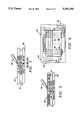
- FIG. 1is a simplified drawing of a prior art digitizing tablet associated with a display panel for use in pen-driven computing applications.
- FIG. 2is a functionally labeled simplified cross section through a prior art digitizing tablet and display panel according to a first embodiment.
- FIG. 3is a functional diagram of the operation of the digitizing tablet of FIG. 2.
- FIG. 4is a functionally labeled simplified cross section through a prior art digitizing tablet and display panel according to a second embodiment.
- FIG. 5is a functionally labeled simplified cross section through a digitizing tablet and display panel according to the basic structure of the present invention in a non-preferred embodiment.
- FIG. 6is a simplified plan view of a basic digitizing tablet grid structure according to the present invention.
- FIG. 7is a detailed cross section of a digitizing tablet associated with a display panel for use in pen-driven computing applications according to the present invention in a non-preferred embodiment thereof.
- FIG. 8is a more detailed cross section of the transparent grid portion of the apparatus of FIG. 5.
- FIG. 9is a functionally labeled simplified cross section through a digitizing tablet and display panel according to the basic structure of the present invention in the preferred embodiment.
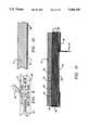
- FIG. 10is an enlarged cross section of a transparent digitizing grid associated with a display panel for use in pen-driven computing applications according to the present invention in the preferred embodiment thereof.
- FIG. 11is a detailed cross section of a digitizing tablet associated with a display panel for use in pen-driven computing applications according to the present invention in the preferred embodiment thereof.
- the basic construction of pen-driven LCD/digitizer input device according to the present invention in a first embodimentis shown in simplified functional cross section in FIG. 5.
- the top surface over which the stylus 18 is movedare the digitizing grids 22'--which in this case are transparent.
- the digitizing grids 22'which in this case are transparent.
- the LCD panel 10Below the transparent digitizing grids 22' is the LCD panel 10 and below that is the backlighting panel 20. How this structure can be obtained and a construction of an LCD/digitizer input device according to this embodiment of the present invention will now be described in detail.
- This particular embodiment of the present inventionis non-preferred in all cases only because the user must view the display through the grid structure of the digitizer. While the grid structure is of film thicknesses, the edges of the transparent conductive runs may still be seen to some slight degree at some times and under some conditions. Thus, the preferred embodiment which eliminates this requirement is the preferred embodiment when it can be used. As will be appreciated, however, the preferred embodiment cannot be employed with all display panels. The greater flexibility of the following, first-described embodiment makes it ideal (and therefore preferred) for such applications.
- the assignee of this applicationmanufactures cordless digitizing tablet systems employing conductive and dielectric inks on flexible substrate materials which are supported by a rigid substrate.
- the preferred LCD/digitizer input device of this inventionemploys a similar construction and utilizes much of the technology therefrom with the LCD panel replacing the rigid substrate.
- the flexible substrate assembly 24 including the transparent digitizing grids 22'is best understood by reference to FIGS. 6-8.
- the flexible substrate assembly 24comprises an outer portion 26 having a rectangular window opening 28 therein.
- An inner portion 30is disposed over the window opening 28. Both the outer portion 26 and the inner portion 30 can be of mylar or a similar material.
- the inner portion 30is sized to fit over the LCD panel 10 to be employed therewith and, accordingly, is transparent.
- the outer portion 26can be transparent or colored, as desired, since it will not be seen.
- the inner portion 30has the transparent digitizing grids 22' formed thereon as transparent X-conductors 32 and transparent Y-conductors 34.
- the conductors 32, 34 depicted in FIG. 6are representative only and in the interest of simplicity are not intended to be to scale or in the proper number. Note also that for the same reason the thickness of layers as depicted in the drawings are not necessarily in relational scale.
- the X-conductors 32are connected according to a loop-back pattern and the Y-conductors 34 are connected according to a straight pattern, which technique was developed by the assignee of this application for use in cordless electromagnetic digitizers.
- the transparent conductors 32, 34were formed of an indium tin oxide (ITO) film material commercially sold under the tradenames Southwall M-20 and Southwall Heatmirror 88.
- ITOindium tin oxide
- the ITO materialwas applied to the mylar substrate material in sheet form and then 2 mil non-conductive strips were etched from the sheet every 0.36 inch to form the conductive runs comprising the transparent conductors 32, 34 (as compared with runs 0.020 to 0.050 inches wide in the prior art).
- the ITO film materialis resistively conducting.
- the transparent inner portion 30 carrying the digitizing grids 22'is formed in two layers.
- a first piece of transparent substrate 36 having ITO transparent conductive material 38 thereon forming the X-conductors 32for example, comprises the first layer with a second piece of transparent substrate 40 having ITO transparent conductive material 42 thereon forming the Y-conductors 34 adhesively attached thereover comprising the second layer.
- the outer portion 26carries a Y-axis connector 44 and an X-axis connector 46 for electrically connecting the flexible substrate 24 to the associated electromagnetic digitizing electronics (not shown) which are generally conventional in nature and form no part of the present invention.
- the Y-axis connector 44 and X-axis connector 46are electrically connected to the Y-conductors 34 and the X-conductors 32, respectively, by conductive ink runs 48 formed on the substrate material of the outer portion 26 in the usual manner.
- the point at which electrical connection is made between the Y-conductors 34 and the X-conductors 32 on the one hand and the conductive ink runs 48 on the other handis accomplished employing a commercially available, electrically conductive, two-sided adhesive tape 50.
- a preferred LCD/digitizing tablet assembly 52 for this embodimentis as shown in FIG. 7.
- the flexible substrate 24is wrapped about the LCD panel 10, which acts as a supporting substrate for the flexible substrate 24.
- a transparent conductive layer of ITO material 54is disposed between the top of the LCD panel 10 and the flexible substrate 24 and connected to ground potential to act as an electrostatic shield to prevent electrostatic charges from interfering with the electromagnetic digitizing process by conducting them to ground.
- the electrostatic shield material 54can be applied to the top of the LCD panel 10 or to the bottom of the flexible substrate 24, as desired for the particular implementation.
- a second shield 56comprising a sheet of aluminum foil non-electrically connected is disposed under the backlighting panel 20 for the further shielding of electromagnetic and electrostatic interference and to aid in the elimination of edge effect problems in the digitizing grids 22'.
- a thin piece of a tough, transparent protective plastic 58 such as polycarbonatebe adhesively attached to the top of the inner portion 30 to prevent damage to the digitizing grids 22' by the stylus 18 in long-term use.
- the foregoing assembly 52can then be disposed in an appropriate case (not shown) which, because of the thin size of the materials involved in the flexible substrate 24 (approximately 0.020 inches total thickness), can be quite thin.
- the thin size of the transparent inner portion 30also allows the LCD panel 10 and the graphic display information displayed thereon by a computer attached thereto to be viewed in most cases without significant interference or distortion.
- FIGS. 9-11The preferred embodiment of the present invention for use with those display panels of a construction which allow its use is shown in FIGS. 9-11.
- the transparent digitizer grids 22'are disposed under the LCD display panel 10 between the LCD display panel 10 and the backlighting panel 20.
- the light from the backlighting panel 20passes through the transparent digitizing grids 22' and from there through the LCD display panel 10.
- the transparent digitizing grids 22'Since the only thing passing through the transparent digitizing grids 22' is an overall illumination from the backlighting panel 20, and edge effects of the conductive runs on the transparent digitizing grids 22' are ineffective in causing any noticeable effect to a viewer viewing a display on the LCD display panel 10.
- the transparent digitizing grids 22'can be applied and formed right on the back surface 68 of the LCD display panel 10 as depicted in simplified form in FIG. 10. Also, since it is only illumination that is passing through the transparent digitizing grids 22', the transparency of the adhesive used to attach the indium tin oxide sheets to the back surface 68 and each other is not so critical. Where in the prior embodiment the adhesive had to be completely transparent because the LCD display panel 10 was viewed through it, in this case a translucent adhesive is entirely acceptable. Thus, in the manufacturing process, a sheet of indium tin oxide for one of the layers of the transparent digitizing grids 22' could be attached to the back surface 68 and then be etched in place to form the conductive runs.
- FIG. 11A preferred construction for this embodiment corresponding to the preferred construction for the prior embodiment of FIG. 7 is shown in FIG. 11.
- the flexible substrate 24, if used,is wrapped about the backlighting panel 20, which acts as a supporting substrate for the flexible substrate 24.
- the LCD panel 10will also contribute to the support.
- a transparent conductive layer of ITO material 54is disposed between the transparent digitizing grids 22' and the top of the backlighting panel 20 and connected to ground potential to act as an electrostatic shield to prevent electrostatic charges from interfering with the electromagnetic digitizing process by conducting them to ground as described in the prior embodiment.
- the electrostatic shield material 54can be applied to the top of the backlighting panel 20 or to the bottom of the flexible substrate 24, as desired for the particular implementation.
- a second shield 56comprising a sheet of aluminum foil non-electrically connected is disposed under the backlighting panel 20 for the further shielding of electromagnetic and electrostatic interference and to aid in the elimination of edge effect problems in the digitizing grids 22'.
- a sheet of a tough, transparent protective plasticsuch as polycarbonate be adhesively attached to the top of the LCD panel 10 to prevent damage thereto by the stylus 18 in long-term use.
Landscapes
- Engineering & Computer Science (AREA)
- General Engineering & Computer Science (AREA)
- Theoretical Computer Science (AREA)
- Physics & Mathematics (AREA)
- Human Computer Interaction (AREA)
- General Physics & Mathematics (AREA)
- Electromagnetism (AREA)
- Position Input By Displaying (AREA)
Abstract
Description
Claims (6)
Priority Applications (6)
| Application Number | Priority Date | Filing Date | Title |
|---|---|---|---|
| US07/784,929US5381160A (en) | 1991-09-27 | 1991-10-30 | See-through digitizer with clear conductive grid |
| TW080109384ATW269026B (en) | 1991-09-27 | 1991-11-28 | |
| JP5508400AJP2934506B2 (en) | 1991-10-30 | 1992-09-25 | Perspective digitizer with transparent conductive grid |
| DE69227917TDE69227917T2 (en) | 1991-10-30 | 1992-09-25 | TRANSPARENT DIGITALIZER WITH CONDUCTIVE TRANSPARENT GRID |
| EP92921248AEP0610262B1 (en) | 1991-10-30 | 1992-09-25 | See-through digitizer with clear conductive grid |
| PCT/US1992/008195WO1993009529A1 (en) | 1991-10-30 | 1992-09-25 | See-through digitizer with clear conductive grid |
Applications Claiming Priority (2)
| Application Number | Priority Date | Filing Date | Title |
|---|---|---|---|
| US76710291A | 1991-09-27 | 1991-09-27 | |
| US07/784,929US5381160A (en) | 1991-09-27 | 1991-10-30 | See-through digitizer with clear conductive grid |
Related Parent Applications (1)
| Application Number | Title | Priority Date | Filing Date |
|---|---|---|---|
| US76710291AContinuation-In-Part | 1991-09-27 | 1991-09-27 |
Publications (1)
| Publication Number | Publication Date |
|---|---|
| US5381160Atrue US5381160A (en) | 1995-01-10 |
Family
ID=25133969
Family Applications (1)
| Application Number | Title | Priority Date | Filing Date |
|---|---|---|---|
| US07/784,929Expired - LifetimeUS5381160A (en) | 1991-09-27 | 1991-10-30 | See-through digitizer with clear conductive grid |
Country Status (6)
| Country | Link |
|---|---|
| US (1) | US5381160A (en) |
| EP (1) | EP0610262B1 (en) |
| JP (1) | JP2934506B2 (en) |
| DE (1) | DE69227917T2 (en) |
| TW (1) | TW269026B (en) |
| WO (1) | WO1993009529A1 (en) |
Cited By (196)
| Publication number | Priority date | Publication date | Assignee | Title |
|---|---|---|---|---|
| US5457289A (en)* | 1994-03-16 | 1995-10-10 | Microtouch Systems, Inc. | Frontally shielded capacitive touch sensor system |
| US5486847A (en)* | 1992-12-21 | 1996-01-23 | Ncr Corporation | Apparatus for a stylus input system for shielding RFI/EMI fields |
| US5548306A (en)* | 1994-04-28 | 1996-08-20 | At&T Global Information Solutions Company | Visible and touchable touch screen shield |
| US5642134A (en)* | 1994-11-17 | 1997-06-24 | Nec Corporation | Integrated tablet device having position detecting function and image display function |
| US5708458A (en)* | 1994-12-15 | 1998-01-13 | Compaq Computer Corporation | Method of and apparatus for using the digitizer sensor loop array of a computing device as an antenna for a radio frequency link to an external data source |
| US5768616A (en)* | 1995-12-13 | 1998-06-16 | Symbios, Inc. | Apparatus for detecting electro-magnetic stylus signals by inducing current into a plurality of sensor coils using signals transmitted by the tranmitter coil of the stylus |
| US5966112A (en)* | 1996-09-13 | 1999-10-12 | Sharp Kabushiki Kaisha | Integrated image-input type display unit |
| WO2001027868A1 (en)* | 1999-10-08 | 2001-04-19 | Synaptics Incorporated | A flexible transparent touch sensing system for electronic devices |
| US6396005B2 (en) | 1998-06-15 | 2002-05-28 | Rodgers Technology Center, Inc. | Method and apparatus for diminishing grid complexity in a tablet |
| US20030040777A1 (en)* | 1996-01-08 | 2003-02-27 | Itzik Shemer | Modulation of intracellular calcium concentration using non-excitatory electrical signals applied to the tissue |
| US20030055464A1 (en)* | 1999-03-05 | 2003-03-20 | Nissim Darvish | Blood glucose level control |
| US6597348B1 (en)* | 1998-12-28 | 2003-07-22 | Semiconductor Energy Laboratory Co., Ltd. | Information-processing device |
| US20030206161A1 (en)* | 2002-05-01 | 2003-11-06 | Fa-Chung Liu | Tablet integrated type monitor filter |
| US20040095333A1 (en)* | 2002-08-29 | 2004-05-20 | N-Trig Ltd. | Transparent digitiser |
| US6747599B2 (en) | 2001-10-11 | 2004-06-08 | Mcewan Technologies, Llc | Radiolocation system having writing pen application |
| US6756970B2 (en) | 1998-11-20 | 2004-06-29 | Microsoft Corporation | Pen-based computer system |
| US20040155871A1 (en)* | 2003-02-10 | 2004-08-12 | N-Trig Ltd. | Touch detection for a digitizer |
| US20040160427A1 (en)* | 1998-11-20 | 2004-08-19 | Microsoft Corporation | Pen-based interface for a notepad computer |
| US20040189888A1 (en)* | 2003-03-28 | 2004-09-30 | Ypu Dong Jae | Liquid crystal display device having electromagnetic sensor |
| US20040249421A1 (en)* | 2000-09-13 | 2004-12-09 | Impulse Dynamics Nv | Blood glucose level control |
| US20050041018A1 (en)* | 2003-08-21 | 2005-02-24 | Harald Philipp | Anisotropic touch screen element |
| US20050062725A1 (en)* | 2001-12-29 | 2005-03-24 | Hsuan-Ming Shih | Touch control display screen with a built-in electromagnet induction layer of septum array grids |
| EP1305650A4 (en)* | 2000-07-28 | 2006-02-08 | N trig ltd | Physical object location apparatus and method and a platform using the same |
| US20060051985A1 (en)* | 2004-09-03 | 2006-03-09 | Industrial Techonology Research Institute | Ultra-thin flexible electronic device |
| US20060085045A1 (en)* | 1999-03-05 | 2006-04-20 | Metacure N.V. | Blood glucose level control |
| US20060184207A1 (en)* | 1999-03-05 | 2006-08-17 | Metacure N.V. | Blood glucose level control |
| US20060262072A1 (en)* | 2005-05-23 | 2006-11-23 | Alps Electric Co., Ltd. | Coordinate input device and terminal device having the same |
| US20070027493A1 (en)* | 2003-07-21 | 2007-02-01 | Shlomo Ben-Haim | Gastrointestinal methods and apparatus for use in treating disorders and controlling blood sugar |
| US20070027487A1 (en)* | 2003-03-10 | 2007-02-01 | Impulse Dynamics Nv | Apparatus and method for delivering electrical signals to modify gene expression in cardiac tissue |
| US20070062852A1 (en)* | 2005-08-11 | 2007-03-22 | N-Trig Ltd. | Apparatus for Object Information Detection and Methods of Using Same |
| US20070240914A1 (en)* | 2006-04-14 | 2007-10-18 | Ritdisplay Corporation | Transparent touch panel |
| US20070279395A1 (en)* | 2006-05-31 | 2007-12-06 | Harald Philipp | Two Dimensional Position Sensor |
| US20070293901A1 (en)* | 2004-03-10 | 2007-12-20 | Impulse Dynamics Nv | Protein activity modification |
| US20080065159A1 (en)* | 1996-01-08 | 2008-03-13 | Shlomo Ben-Haim | Electrical Muscle Controller |
| US20080062139A1 (en)* | 2006-06-09 | 2008-03-13 | Apple Inc. | Touch screen liquid crystal display |
| WO2007084467A3 (en)* | 2006-01-17 | 2008-04-17 | World Properties Inc | Capacitive touch sensor with integral el backlight |
| US20080117184A1 (en)* | 2000-11-30 | 2008-05-22 | Palm, Inc. | Flexible screen display with touch sensor in a portable computer |
| US20080140142A1 (en)* | 1996-01-08 | 2008-06-12 | Nissim Darvish | Electrical muscle controller and pacing with hemodynamic enhancement |
| US20080150914A1 (en)* | 2006-12-25 | 2008-06-26 | Sadao Yamamoto | Position detecting device and display device |
| US20080160795A1 (en)* | 2004-11-10 | 2008-07-03 | Industrial Technology Research Institute | Ultra-thin flexible electronic device |
| US20080157867A1 (en)* | 2007-01-03 | 2008-07-03 | Apple Inc. | Individual channel phase delay scheme |
| US20080165158A1 (en)* | 2007-01-05 | 2008-07-10 | Apple Inc. | Touch screen stack-ups |
| US20080164077A1 (en)* | 2006-11-28 | 2008-07-10 | Sadao Yamamoto | Position detecting device and display device |
| US7408838B1 (en) | 2007-01-22 | 2008-08-05 | Scale Master Technologies, Llc | Digitizing planimeter |
| US20080238881A1 (en)* | 2007-03-27 | 2008-10-02 | N-Trig Ltd. | Shield for a digitizer sensor |
| US20080264699A1 (en)* | 2007-04-27 | 2008-10-30 | Trendon Touch Technology Corp. | Conductor pattern structure of capacitive touch panel |
| US20090004738A1 (en)* | 1999-02-04 | 2009-01-01 | Pluristem Life Systems Inc. | Method and apparatus for maintenance and expansion of hemopoietic stem cells and/or progenitor cells |
| US20090062893A1 (en)* | 2005-03-18 | 2009-03-05 | Meta Cure Limited | Pancreas lead |
| US20090085894A1 (en)* | 2007-09-28 | 2009-04-02 | Unidym, Inc. | Multipoint nanostructure-film touch screen |
| US20090088816A1 (en)* | 1999-03-05 | 2009-04-02 | Tami Harel | Gastrointestinal Methods And Apparatus For Use In Treating Disorders And Controlling Blood Sugar |
| US20090131993A1 (en)* | 1999-03-05 | 2009-05-21 | Benny Rousso | Non-Immediate Effects of Therapy |
| US20090292324A1 (en)* | 2003-03-10 | 2009-11-26 | Benny Rousso | Protein activity modification |
| US20100016923A1 (en)* | 2004-03-10 | 2010-01-21 | Impulse Dynamics Nv | Protein activity modification |
| US7688315B1 (en)* | 2000-11-30 | 2010-03-30 | Palm, Inc. | Proximity input detection system for an electronic device |
| US20100164890A1 (en)* | 2008-12-26 | 2010-07-01 | Kyubok Lee | Input device for flexible display device and manufacturing method thereof |
| US20100331739A1 (en)* | 2007-05-09 | 2010-12-30 | S.A.E Afikim | Method and system for predicting calving |
| US20110187677A1 (en)* | 2006-06-09 | 2011-08-04 | Steve Porter Hotelling | Segmented vcom |
| US8125463B2 (en) | 2004-05-06 | 2012-02-28 | Apple Inc. | Multipoint touchscreen |
| USRE43931E1 (en) | 1997-12-30 | 2013-01-15 | Ericsson Inc. | Radiotelephones having contact-sensitive user interfaces and methods of operating same |
| CN103354188A (en)* | 2013-06-04 | 2013-10-16 | 苏州达方电子有限公司 | Illuminant keyboard and light guide plate module thereof and manufacture method of light guide plate module |
| US8605050B2 (en) | 2007-08-21 | 2013-12-10 | Tpk Touch Solutions (Xiamen) Inc. | Conductor pattern structure of capacitive touch panel |
| US8655444B2 (en) | 1996-01-08 | 2014-02-18 | Impulse Dynamics, N.V. | Electrical muscle controller |
| US8654083B2 (en) | 2006-06-09 | 2014-02-18 | Apple Inc. | Touch screen liquid crystal display |
| US8743300B2 (en) | 2010-12-22 | 2014-06-03 | Apple Inc. | Integrated touch screens |
| US8934975B2 (en) | 2010-02-01 | 2015-01-13 | Metacure Limited | Gastrointestinal electrical therapy |
| US8963856B2 (en) | 2011-06-15 | 2015-02-24 | Tpk Touch Solutions Inc. | Touch sensing layer and manufacturing method thereof |
| US9289618B1 (en) | 1996-01-08 | 2016-03-22 | Impulse Dynamics Nv | Electrical muscle controller |
| US9395857B2 (en) | 2007-12-24 | 2016-07-19 | Tpk Holding Co., Ltd. | Capacitive touch panel |
| US9667317B2 (en) | 2015-06-15 | 2017-05-30 | At&T Intellectual Property I, L.P. | Method and apparatus for providing security using network traffic adjustments |
| US9674711B2 (en) | 2013-11-06 | 2017-06-06 | At&T Intellectual Property I, L.P. | Surface-wave communications and methods thereof |
| US9685992B2 (en) | 2014-10-03 | 2017-06-20 | At&T Intellectual Property I, L.P. | Circuit panel network and methods thereof |
| US9705610B2 (en) | 2014-10-21 | 2017-07-11 | At&T Intellectual Property I, L.P. | Transmission device with impairment compensation and methods for use therewith |
| US9705561B2 (en) | 2015-04-24 | 2017-07-11 | At&T Intellectual Property I, L.P. | Directional coupling device and methods for use therewith |
| US9713723B2 (en) | 1996-01-11 | 2017-07-25 | Impulse Dynamics Nv | Signal delivery through the right ventricular septum |
| US9722318B2 (en) | 2015-07-14 | 2017-08-01 | At&T Intellectual Property I, L.P. | Method and apparatus for coupling an antenna to a device |
| US9729197B2 (en) | 2015-10-01 | 2017-08-08 | At&T Intellectual Property I, L.P. | Method and apparatus for communicating network management traffic over a network |
| US9735833B2 (en) | 2015-07-31 | 2017-08-15 | At&T Intellectual Property I, L.P. | Method and apparatus for communications management in a neighborhood network |
| US9742462B2 (en) | 2014-12-04 | 2017-08-22 | At&T Intellectual Property I, L.P. | Transmission medium and communication interfaces and methods for use therewith |
| US9742521B2 (en) | 2014-11-20 | 2017-08-22 | At&T Intellectual Property I, L.P. | Transmission device with mode division multiplexing and methods for use therewith |
| US9749013B2 (en) | 2015-03-17 | 2017-08-29 | At&T Intellectual Property I, L.P. | Method and apparatus for reducing attenuation of electromagnetic waves guided by a transmission medium |
| US9749053B2 (en) | 2015-07-23 | 2017-08-29 | At&T Intellectual Property I, L.P. | Node device, repeater and methods for use therewith |
| US9748626B2 (en) | 2015-05-14 | 2017-08-29 | At&T Intellectual Property I, L.P. | Plurality of cables having different cross-sectional shapes which are bundled together to form a transmission medium |
| US9769128B2 (en) | 2015-09-28 | 2017-09-19 | At&T Intellectual Property I, L.P. | Method and apparatus for encryption of communications over a network |
| US9769020B2 (en) | 2014-10-21 | 2017-09-19 | At&T Intellectual Property I, L.P. | Method and apparatus for responding to events affecting communications in a communication network |
| US9768833B2 (en) | 2014-09-15 | 2017-09-19 | At&T Intellectual Property I, L.P. | Method and apparatus for sensing a condition in a transmission medium of electromagnetic waves |
| US9780834B2 (en) | 2014-10-21 | 2017-10-03 | At&T Intellectual Property I, L.P. | Method and apparatus for transmitting electromagnetic waves |
| US9787412B2 (en) | 2015-06-25 | 2017-10-10 | At&T Intellectual Property I, L.P. | Methods and apparatus for inducing a fundamental wave mode on a transmission medium |
| US9793955B2 (en) | 2015-04-24 | 2017-10-17 | At&T Intellectual Property I, Lp | Passive electrical coupling device and methods for use therewith |
| US9793951B2 (en) | 2015-07-15 | 2017-10-17 | At&T Intellectual Property I, L.P. | Method and apparatus for launching a wave mode that mitigates interference |
| US9793954B2 (en) | 2015-04-28 | 2017-10-17 | At&T Intellectual Property I, L.P. | Magnetic coupling device and methods for use therewith |
| US9800327B2 (en) | 2014-11-20 | 2017-10-24 | At&T Intellectual Property I, L.P. | Apparatus for controlling operations of a communication device and methods thereof |
| US9820146B2 (en) | 2015-06-12 | 2017-11-14 | At&T Intellectual Property I, L.P. | Method and apparatus for authentication and identity management of communicating devices |
| US9838078B2 (en) | 2015-07-31 | 2017-12-05 | At&T Intellectual Property I, L.P. | Method and apparatus for exchanging communication signals |
| US9838896B1 (en) | 2016-12-09 | 2017-12-05 | At&T Intellectual Property I, L.P. | Method and apparatus for assessing network coverage |
| US9847850B2 (en) | 2014-10-14 | 2017-12-19 | At&T Intellectual Property I, L.P. | Method and apparatus for adjusting a mode of communication in a communication network |
| US9847566B2 (en) | 2015-07-14 | 2017-12-19 | At&T Intellectual Property I, L.P. | Method and apparatus for adjusting a field of a signal to mitigate interference |
| US9853342B2 (en) | 2015-07-14 | 2017-12-26 | At&T Intellectual Property I, L.P. | Dielectric transmission medium connector and methods for use therewith |
| US9860075B1 (en) | 2016-08-26 | 2018-01-02 | At&T Intellectual Property I, L.P. | Method and communication node for broadband distribution |
| US9866309B2 (en) | 2015-06-03 | 2018-01-09 | At&T Intellectual Property I, Lp | Host node device and methods for use therewith |
| US9866276B2 (en) | 2014-10-10 | 2018-01-09 | At&T Intellectual Property I, L.P. | Method and apparatus for arranging communication sessions in a communication system |
| US9865911B2 (en) | 2015-06-25 | 2018-01-09 | At&T Intellectual Property I, L.P. | Waveguide system for slot radiating first electromagnetic waves that are combined into a non-fundamental wave mode second electromagnetic wave on a transmission medium |
| US9871282B2 (en) | 2015-05-14 | 2018-01-16 | At&T Intellectual Property I, L.P. | At least one transmission medium having a dielectric surface that is covered at least in part by a second dielectric |
| US9871283B2 (en) | 2015-07-23 | 2018-01-16 | At&T Intellectual Property I, Lp | Transmission medium having a dielectric core comprised of plural members connected by a ball and socket configuration |
| US9871558B2 (en) | 2014-10-21 | 2018-01-16 | At&T Intellectual Property I, L.P. | Guided-wave transmission device and methods for use therewith |
| US9876605B1 (en) | 2016-10-21 | 2018-01-23 | At&T Intellectual Property I, L.P. | Launcher and coupling system to support desired guided wave mode |
| US9876264B2 (en) | 2015-10-02 | 2018-01-23 | At&T Intellectual Property I, Lp | Communication system, guided wave switch and methods for use therewith |
| US9876570B2 (en) | 2015-02-20 | 2018-01-23 | At&T Intellectual Property I, Lp | Guided-wave transmission device with non-fundamental mode propagation and methods for use therewith |
| US9882257B2 (en) | 2015-07-14 | 2018-01-30 | At&T Intellectual Property I, L.P. | Method and apparatus for launching a wave mode that mitigates interference |
| US9887447B2 (en) | 2015-05-14 | 2018-02-06 | At&T Intellectual Property I, L.P. | Transmission medium having multiple cores and methods for use therewith |
| US9893795B1 (en) | 2016-12-07 | 2018-02-13 | At&T Intellectual Property I, Lp | Method and repeater for broadband distribution |
| US9906269B2 (en) | 2014-09-17 | 2018-02-27 | At&T Intellectual Property I, L.P. | Monitoring and mitigating conditions in a communication network |
| US9904535B2 (en) | 2015-09-14 | 2018-02-27 | At&T Intellectual Property I, L.P. | Method and apparatus for distributing software |
| US9912381B2 (en) | 2015-06-03 | 2018-03-06 | At&T Intellectual Property I, Lp | Network termination and methods for use therewith |
| US9912027B2 (en) | 2015-07-23 | 2018-03-06 | At&T Intellectual Property I, L.P. | Method and apparatus for exchanging communication signals |
| US9912033B2 (en) | 2014-10-21 | 2018-03-06 | At&T Intellectual Property I, Lp | Guided wave coupler, coupling module and methods for use therewith |
| US9913139B2 (en) | 2015-06-09 | 2018-03-06 | At&T Intellectual Property I, L.P. | Signal fingerprinting for authentication of communicating devices |
| US9911020B1 (en) | 2016-12-08 | 2018-03-06 | At&T Intellectual Property I, L.P. | Method and apparatus for tracking via a radio frequency identification device |
| US9917341B2 (en) | 2015-05-27 | 2018-03-13 | At&T Intellectual Property I, L.P. | Apparatus and method for launching electromagnetic waves and for modifying radial dimensions of the propagating electromagnetic waves |
| US9929755B2 (en) | 2015-07-14 | 2018-03-27 | At&T Intellectual Property I, L.P. | Method and apparatus for coupling an antenna to a device |
| US9927517B1 (en) | 2016-12-06 | 2018-03-27 | At&T Intellectual Property I, L.P. | Apparatus and methods for sensing rainfall |
| US9948333B2 (en) | 2015-07-23 | 2018-04-17 | At&T Intellectual Property I, L.P. | Method and apparatus for wireless communications to mitigate interference |
| US9954286B2 (en) | 2014-10-21 | 2018-04-24 | At&T Intellectual Property I, L.P. | Guided-wave transmission device with non-fundamental mode propagation and methods for use therewith |
| US9954287B2 (en) | 2014-11-20 | 2018-04-24 | At&T Intellectual Property I, L.P. | Apparatus for converting wireless signals and electromagnetic waves and methods thereof |
| US9967173B2 (en) | 2015-07-31 | 2018-05-08 | At&T Intellectual Property I, L.P. | Method and apparatus for authentication and identity management of communicating devices |
| US9973416B2 (en) | 2014-10-02 | 2018-05-15 | At&T Intellectual Property I, L.P. | Method and apparatus that provides fault tolerance in a communication network |
| US9973940B1 (en) | 2017-02-27 | 2018-05-15 | At&T Intellectual Property I, L.P. | Apparatus and methods for dynamic impedance matching of a guided wave launcher |
| US9991580B2 (en) | 2016-10-21 | 2018-06-05 | At&T Intellectual Property I, L.P. | Launcher and coupling system for guided wave mode cancellation |
| US9999038B2 (en) | 2013-05-31 | 2018-06-12 | At&T Intellectual Property I, L.P. | Remote distributed antenna system |
| US9997819B2 (en) | 2015-06-09 | 2018-06-12 | At&T Intellectual Property I, L.P. | Transmission medium and method for facilitating propagation of electromagnetic waves via a core |
| US9998870B1 (en) | 2016-12-08 | 2018-06-12 | At&T Intellectual Property I, L.P. | Method and apparatus for proximity sensing |
| US10009067B2 (en) | 2014-12-04 | 2018-06-26 | At&T Intellectual Property I, L.P. | Method and apparatus for configuring a communication interface |
| US10020844B2 (en) | 2016-12-06 | 2018-07-10 | T&T Intellectual Property I, L.P. | Method and apparatus for broadcast communication via guided waves |
| US10027397B2 (en) | 2016-12-07 | 2018-07-17 | At&T Intellectual Property I, L.P. | Distributed antenna system and methods for use therewith |
| US10044409B2 (en) | 2015-07-14 | 2018-08-07 | At&T Intellectual Property I, L.P. | Transmission medium and methods for use therewith |
| US10051630B2 (en) | 2013-05-31 | 2018-08-14 | At&T Intellectual Property I, L.P. | Remote distributed antenna system |
| US10069185B2 (en) | 2015-06-25 | 2018-09-04 | At&T Intellectual Property I, L.P. | Methods and apparatus for inducing a non-fundamental wave mode on a transmission medium |
| US10069535B2 (en) | 2016-12-08 | 2018-09-04 | At&T Intellectual Property I, L.P. | Apparatus and methods for launching electromagnetic waves having a certain electric field structure |
| US10090594B2 (en) | 2016-11-23 | 2018-10-02 | At&T Intellectual Property I, L.P. | Antenna system having structural configurations for assembly |
| US10090606B2 (en) | 2015-07-15 | 2018-10-02 | At&T Intellectual Property I, L.P. | Antenna system with dielectric array and methods for use therewith |
| US10103422B2 (en) | 2016-12-08 | 2018-10-16 | At&T Intellectual Property I, L.P. | Method and apparatus for mounting network devices |
| US10135145B2 (en) | 2016-12-06 | 2018-11-20 | At&T Intellectual Property I, L.P. | Apparatus and methods for generating an electromagnetic wave along a transmission medium |
| US10136255B2 (en) | 2016-12-08 | 2018-11-20 | At&T Intellectual Property I, L.P. | Method and apparatus for proximity sensing on a communication device |
| US10135146B2 (en) | 2016-10-18 | 2018-11-20 | At&T Intellectual Property I, L.P. | Apparatus and methods for launching guided waves via circuits |
| US10135147B2 (en) | 2016-10-18 | 2018-11-20 | At&T Intellectual Property I, L.P. | Apparatus and methods for launching guided waves via an antenna |
| US10139820B2 (en) | 2016-12-07 | 2018-11-27 | At&T Intellectual Property I, L.P. | Method and apparatus for deploying equipment of a communication system |
| US10148016B2 (en) | 2015-07-14 | 2018-12-04 | At&T Intellectual Property I, L.P. | Apparatus and methods for communicating utilizing an antenna array |
| US10168695B2 (en) | 2016-12-07 | 2019-01-01 | At&T Intellectual Property I, L.P. | Method and apparatus for controlling an unmanned aircraft |
| US10178445B2 (en) | 2016-11-23 | 2019-01-08 | At&T Intellectual Property I, L.P. | Methods, devices, and systems for load balancing between a plurality of waveguides |
| US10205655B2 (en) | 2015-07-14 | 2019-02-12 | At&T Intellectual Property I, L.P. | Apparatus and methods for communicating utilizing an antenna array and multiple communication paths |
| US10225025B2 (en) | 2016-11-03 | 2019-03-05 | At&T Intellectual Property I, L.P. | Method and apparatus for detecting a fault in a communication system |
| US10224634B2 (en) | 2016-11-03 | 2019-03-05 | At&T Intellectual Property I, L.P. | Methods and apparatus for adjusting an operational characteristic of an antenna |
| US10243784B2 (en) | 2014-11-20 | 2019-03-26 | At&T Intellectual Property I, L.P. | System for generating topology information and methods thereof |
| US10243270B2 (en) | 2016-12-07 | 2019-03-26 | At&T Intellectual Property I, L.P. | Beam adaptive multi-feed dielectric antenna system and methods for use therewith |
| US10248265B2 (en) | 2014-12-31 | 2019-04-02 | Nihat Deniz Bayramoglu | Touch detecting panel |
| US10264586B2 (en) | 2016-12-09 | 2019-04-16 | At&T Mobility Ii Llc | Cloud-based packet controller and methods for use therewith |
| US10282040B2 (en) | 2009-03-20 | 2019-05-07 | Tpk Touch Solutions (Xiamen) Inc. | Capacitive touch circuit pattern and manufacturing method thereof |
| US10291334B2 (en) | 2016-11-03 | 2019-05-14 | At&T Intellectual Property I, L.P. | System for detecting a fault in a communication system |
| US10298293B2 (en) | 2017-03-13 | 2019-05-21 | At&T Intellectual Property I, L.P. | Apparatus of communication utilizing wireless network devices |
| US10305190B2 (en) | 2016-12-01 | 2019-05-28 | At&T Intellectual Property I, L.P. | Reflecting dielectric antenna system and methods for use therewith |
| US10312567B2 (en) | 2016-10-26 | 2019-06-04 | At&T Intellectual Property I, L.P. | Launcher with planar strip antenna and methods for use therewith |
| US10320586B2 (en) | 2015-07-14 | 2019-06-11 | At&T Intellectual Property I, L.P. | Apparatus and methods for generating non-interfering electromagnetic waves on an insulated transmission medium |
| US10326494B2 (en) | 2016-12-06 | 2019-06-18 | At&T Intellectual Property I, L.P. | Apparatus for measurement de-embedding and methods for use therewith |
| US10326689B2 (en) | 2016-12-08 | 2019-06-18 | At&T Intellectual Property I, L.P. | Method and system for providing alternative communication paths |
| US10340983B2 (en) | 2016-12-09 | 2019-07-02 | At&T Intellectual Property I, L.P. | Method and apparatus for surveying remote sites via guided wave communications |
| US10340601B2 (en) | 2016-11-23 | 2019-07-02 | At&T Intellectual Property I, L.P. | Multi-antenna system and methods for use therewith |
| US10340573B2 (en) | 2016-10-26 | 2019-07-02 | At&T Intellectual Property I, L.P. | Launcher with cylindrical coupling device and methods for use therewith |
| US10340600B2 (en) | 2016-10-18 | 2019-07-02 | At&T Intellectual Property I, L.P. | Apparatus and methods for launching guided waves via plural waveguide systems |
| US10340603B2 (en) | 2016-11-23 | 2019-07-02 | At&T Intellectual Property I, L.P. | Antenna system having shielded structural configurations for assembly |
| US10355367B2 (en) | 2015-10-16 | 2019-07-16 | At&T Intellectual Property I, L.P. | Antenna structure for exchanging wireless signals |
| US10361489B2 (en) | 2016-12-01 | 2019-07-23 | At&T Intellectual Property I, L.P. | Dielectric dish antenna system and methods for use therewith |
| US10359749B2 (en) | 2016-12-07 | 2019-07-23 | At&T Intellectual Property I, L.P. | Method and apparatus for utilities management via guided wave communication |
| US10374316B2 (en) | 2016-10-21 | 2019-08-06 | At&T Intellectual Property I, L.P. | System and dielectric antenna with non-uniform dielectric |
| US10382976B2 (en) | 2016-12-06 | 2019-08-13 | At&T Intellectual Property I, L.P. | Method and apparatus for managing wireless communications based on communication paths and network device positions |
| US10389037B2 (en) | 2016-12-08 | 2019-08-20 | At&T Intellectual Property I, L.P. | Apparatus and methods for selecting sections of an antenna array and use therewith |
| US10389029B2 (en) | 2016-12-07 | 2019-08-20 | At&T Intellectual Property I, L.P. | Multi-feed dielectric antenna system with core selection and methods for use therewith |
| US10411356B2 (en) | 2016-12-08 | 2019-09-10 | At&T Intellectual Property I, L.P. | Apparatus and methods for selectively targeting communication devices with an antenna array |
| US10439675B2 (en) | 2016-12-06 | 2019-10-08 | At&T Intellectual Property I, L.P. | Method and apparatus for repeating guided wave communication signals |
| US10446936B2 (en) | 2016-12-07 | 2019-10-15 | At&T Intellectual Property I, L.P. | Multi-feed dielectric antenna system and methods for use therewith |
| US10498044B2 (en) | 2016-11-03 | 2019-12-03 | At&T Intellectual Property I, L.P. | Apparatus for configuring a surface of an antenna |
| US10530505B2 (en) | 2016-12-08 | 2020-01-07 | At&T Intellectual Property I, L.P. | Apparatus and methods for launching electromagnetic waves along a transmission medium |
| US10535928B2 (en) | 2016-11-23 | 2020-01-14 | At&T Intellectual Property I, L.P. | Antenna system and methods for use therewith |
| US10547348B2 (en) | 2016-12-07 | 2020-01-28 | At&T Intellectual Property I, L.P. | Method and apparatus for switching transmission mediums in a communication system |
| US10601494B2 (en) | 2016-12-08 | 2020-03-24 | At&T Intellectual Property I, L.P. | Dual-band communication device and method for use therewith |
| US10637149B2 (en) | 2016-12-06 | 2020-04-28 | At&T Intellectual Property I, L.P. | Injection molded dielectric antenna and methods for use therewith |
| US10650940B2 (en) | 2015-05-15 | 2020-05-12 | At&T Intellectual Property I, L.P. | Transmission medium having a conductive material and methods for use therewith |
| US10694379B2 (en) | 2016-12-06 | 2020-06-23 | At&T Intellectual Property I, L.P. | Waveguide system with device-based authentication and methods for use therewith |
| US10727599B2 (en) | 2016-12-06 | 2020-07-28 | At&T Intellectual Property I, L.P. | Launcher with slot antenna and methods for use therewith |
| US10755542B2 (en) | 2016-12-06 | 2020-08-25 | At&T Intellectual Property I, L.P. | Method and apparatus for surveillance via guided wave communication |
| US10777873B2 (en) | 2016-12-08 | 2020-09-15 | At&T Intellectual Property I, L.P. | Method and apparatus for mounting network devices |
| US10797781B2 (en) | 2015-06-03 | 2020-10-06 | At&T Intellectual Property I, L.P. | Client node device and methods for use therewith |
| US10811767B2 (en) | 2016-10-21 | 2020-10-20 | At&T Intellectual Property I, L.P. | System and dielectric antenna with convex dielectric radome |
| US10819035B2 (en) | 2016-12-06 | 2020-10-27 | At&T Intellectual Property I, L.P. | Launcher with helical antenna and methods for use therewith |
| US10916969B2 (en) | 2016-12-08 | 2021-02-09 | At&T Intellectual Property I, L.P. | Method and apparatus for providing power using an inductive coupling |
| US10938108B2 (en) | 2016-12-08 | 2021-03-02 | At&T Intellectual Property I, L.P. | Frequency selective multi-feed dielectric antenna system and methods for use therewith |
| US11439815B2 (en) | 2003-03-10 | 2022-09-13 | Impulse Dynamics Nv | Protein activity modification |
| US11779768B2 (en) | 2004-03-10 | 2023-10-10 | Impulse Dynamics Nv | Protein activity modification |
Families Citing this family (3)
| Publication number | Priority date | Publication date | Assignee | Title |
|---|---|---|---|---|
| US5834709A (en)* | 1994-01-26 | 1998-11-10 | Lucent Technologies Inc. | Position sensing systems including magnetoresistive elements |
| AU2003295167A1 (en) | 2003-01-07 | 2004-07-29 | Sensopad Limited | Sensing apparatus and method |
| GB0300291D0 (en)* | 2003-01-07 | 2003-02-05 | Sensopad Technologies Ltd | Position encoder |
Citations (7)
| Publication number | Priority date | Publication date | Assignee | Title |
|---|---|---|---|---|
| US4523654A (en)* | 1983-09-14 | 1985-06-18 | Scriptel Corporation | Electrographic system |
| US4639720A (en)* | 1981-01-12 | 1987-01-27 | Harris Corporation | Electronic sketch pad |
| US4704501A (en)* | 1984-12-28 | 1987-11-03 | Wacom Co., Ltd. | Position detecting device |
| US4853499A (en)* | 1988-12-12 | 1989-08-01 | Calcomp Inc. | Ground switching technique for silkscreened digitizer grids |
| US4945348A (en)* | 1987-04-22 | 1990-07-31 | Hitachi Ltd. | Liquid crystal display combined with signal input tablet |
| US4988837A (en)* | 1987-12-25 | 1991-01-29 | Wacom Co., Ltd. | Position detecting device |
| US5149919A (en)* | 1990-10-31 | 1992-09-22 | International Business Machines Corporation | Stylus sensing system |
- 1991
- 1991-10-30USUS07/784,929patent/US5381160A/ennot_activeExpired - Lifetime
- 1991-11-28TWTW080109384Apatent/TW269026B/zhactive
- 1992
- 1992-09-25WOPCT/US1992/008195patent/WO1993009529A1/enactiveIP Right Grant
- 1992-09-25EPEP92921248Apatent/EP0610262B1/ennot_activeExpired - Lifetime
- 1992-09-25DEDE69227917Tpatent/DE69227917T2/ennot_activeExpired - Fee Related
- 1992-09-25JPJP5508400Apatent/JP2934506B2/ennot_activeExpired - Lifetime
Patent Citations (7)
| Publication number | Priority date | Publication date | Assignee | Title |
|---|---|---|---|---|
| US4639720A (en)* | 1981-01-12 | 1987-01-27 | Harris Corporation | Electronic sketch pad |
| US4523654A (en)* | 1983-09-14 | 1985-06-18 | Scriptel Corporation | Electrographic system |
| US4704501A (en)* | 1984-12-28 | 1987-11-03 | Wacom Co., Ltd. | Position detecting device |
| US4945348A (en)* | 1987-04-22 | 1990-07-31 | Hitachi Ltd. | Liquid crystal display combined with signal input tablet |
| US4988837A (en)* | 1987-12-25 | 1991-01-29 | Wacom Co., Ltd. | Position detecting device |
| US4853499A (en)* | 1988-12-12 | 1989-08-01 | Calcomp Inc. | Ground switching technique for silkscreened digitizer grids |
| US5149919A (en)* | 1990-10-31 | 1992-09-22 | International Business Machines Corporation | Stylus sensing system |
Cited By (315)
| Publication number | Priority date | Publication date | Assignee | Title |
|---|---|---|---|---|
| US5486847A (en)* | 1992-12-21 | 1996-01-23 | Ncr Corporation | Apparatus for a stylus input system for shielding RFI/EMI fields |
| US5457289A (en)* | 1994-03-16 | 1995-10-10 | Microtouch Systems, Inc. | Frontally shielded capacitive touch sensor system |
| US5548306A (en)* | 1994-04-28 | 1996-08-20 | At&T Global Information Solutions Company | Visible and touchable touch screen shield |
| US5642134A (en)* | 1994-11-17 | 1997-06-24 | Nec Corporation | Integrated tablet device having position detecting function and image display function |
| US5708458A (en)* | 1994-12-15 | 1998-01-13 | Compaq Computer Corporation | Method of and apparatus for using the digitizer sensor loop array of a computing device as an antenna for a radio frequency link to an external data source |
| US5768616A (en)* | 1995-12-13 | 1998-06-16 | Symbios, Inc. | Apparatus for detecting electro-magnetic stylus signals by inducing current into a plurality of sensor coils using signals transmitted by the tranmitter coil of the stylus |
| US8306616B2 (en) | 1996-01-08 | 2012-11-06 | Impulse Dynamics, N.V. | Electrical muscle controller |
| US20080065164A1 (en)* | 1996-01-08 | 2008-03-13 | Shlomo Ben-Haim | Electrical Muscle Controller |
| US8958872B2 (en) | 1996-01-08 | 2015-02-17 | Impulse Dynamics, N.V. | Electrical muscle controller |
| US20030040777A1 (en)* | 1996-01-08 | 2003-02-27 | Itzik Shemer | Modulation of intracellular calcium concentration using non-excitatory electrical signals applied to the tissue |
| US8260416B2 (en) | 1996-01-08 | 2012-09-04 | Impulse Dynamics, N.V. | Electrical muscle controller |
| US8301247B2 (en) | 1996-01-08 | 2012-10-30 | Impulse Dynamics, N.V. | Electrical muscle controller |
| US8306617B2 (en) | 1996-01-08 | 2012-11-06 | Impulse Dynamics N.V. | Electrical muscle controller |
| US8655444B2 (en) | 1996-01-08 | 2014-02-18 | Impulse Dynamics, N.V. | Electrical muscle controller |
| US20070239216A9 (en)* | 1996-01-08 | 2007-10-11 | Itzik Shemer | Modulation of intracellular calcium concentration using non-excitatory electrical signals applied to the tissue |
| US8311629B2 (en) | 1996-01-08 | 2012-11-13 | Impulse Dynamics, N.V. | Electrical muscle controller |
| US8321013B2 (en) | 1996-01-08 | 2012-11-27 | Impulse Dynamics, N.V. | Electrical muscle controller and pacing with hemodynamic enhancement |
| US20080065159A1 (en)* | 1996-01-08 | 2008-03-13 | Shlomo Ben-Haim | Electrical Muscle Controller |
| US9289618B1 (en) | 1996-01-08 | 2016-03-22 | Impulse Dynamics Nv | Electrical muscle controller |
| US9186514B2 (en) | 1996-01-08 | 2015-11-17 | Impulse Dynamics Nv | Electrical muscle controller |
| US8825152B2 (en) | 1996-01-08 | 2014-09-02 | Impulse Dynamics, N.V. | Modulation of intracellular calcium concentration using non-excitatory electrical signals applied to the tissue |
| US20080140142A1 (en)* | 1996-01-08 | 2008-06-12 | Nissim Darvish | Electrical muscle controller and pacing with hemodynamic enhancement |
| US20080065163A1 (en)* | 1996-01-08 | 2008-03-13 | Shlomo Ben-Haim | Electrical Muscle Controller |
| US9713723B2 (en) | 1996-01-11 | 2017-07-25 | Impulse Dynamics Nv | Signal delivery through the right ventricular septum |
| US5966112A (en)* | 1996-09-13 | 1999-10-12 | Sharp Kabushiki Kaisha | Integrated image-input type display unit |
| USRE43931E1 (en) | 1997-12-30 | 2013-01-15 | Ericsson Inc. | Radiotelephones having contact-sensitive user interfaces and methods of operating same |
| US8812059B2 (en) | 1997-12-30 | 2014-08-19 | Ericsson, Inc. | Radiotelephones having contact-sensitive user interfaces and methods of operating same |
| US6396005B2 (en) | 1998-06-15 | 2002-05-28 | Rodgers Technology Center, Inc. | Method and apparatus for diminishing grid complexity in a tablet |
| US20050198593A1 (en)* | 1998-11-20 | 2005-09-08 | Microsoft Corporation | Pen-based interface for a notepad computer |
| US20050198592A1 (en)* | 1998-11-20 | 2005-09-08 | Microsoft Corporation | Pen-based interface for a notepad computer |
| US20040160427A1 (en)* | 1998-11-20 | 2004-08-19 | Microsoft Corporation | Pen-based interface for a notepad computer |
| US7032187B2 (en) | 1998-11-20 | 2006-04-18 | Microsoft Corporation | Pen-based interface for a notepad computer |
| US20050204301A1 (en)* | 1998-11-20 | 2005-09-15 | Microsoft Corporation | Pen-based interface for a notepad computer |
| US7559037B2 (en) | 1998-11-20 | 2009-07-07 | Microsoft Corporation | Pen-based interface for a notepad computer |
| US6756970B2 (en) | 1998-11-20 | 2004-06-29 | Microsoft Corporation | Pen-based computer system |
| US7703047B2 (en) | 1998-11-20 | 2010-04-20 | Microsoft Corporation | Pen-based interface for a notepad computer |
| US7825897B2 (en) | 1998-11-20 | 2010-11-02 | Microsoft Corporation | Pen-based interface for a notepad computer |
| US6597348B1 (en)* | 1998-12-28 | 2003-07-22 | Semiconductor Energy Laboratory Co., Ltd. | Information-processing device |
| US20090004738A1 (en)* | 1999-02-04 | 2009-01-01 | Pluristem Life Systems Inc. | Method and apparatus for maintenance and expansion of hemopoietic stem cells and/or progenitor cells |
| US20060184207A1 (en)* | 1999-03-05 | 2006-08-17 | Metacure N.V. | Blood glucose level control |
| US20090088816A1 (en)* | 1999-03-05 | 2009-04-02 | Tami Harel | Gastrointestinal Methods And Apparatus For Use In Treating Disorders And Controlling Blood Sugar |
| US20030055464A1 (en)* | 1999-03-05 | 2003-03-20 | Nissim Darvish | Blood glucose level control |
| US8346363B2 (en) | 1999-03-05 | 2013-01-01 | Metacure Limited | Blood glucose level control |
| US8666495B2 (en) | 1999-03-05 | 2014-03-04 | Metacure Limited | Gastrointestinal methods and apparatus for use in treating disorders and controlling blood sugar |
| US8019421B2 (en) | 1999-03-05 | 2011-09-13 | Metacure Limited | Blood glucose level control |
| US8700161B2 (en) | 1999-03-05 | 2014-04-15 | Metacure Limited | Blood glucose level control |
| US20090131993A1 (en)* | 1999-03-05 | 2009-05-21 | Benny Rousso | Non-Immediate Effects of Therapy |
| US20060085045A1 (en)* | 1999-03-05 | 2006-04-20 | Metacure N.V. | Blood glucose level control |
| US9101765B2 (en) | 1999-03-05 | 2015-08-11 | Metacure Limited | Non-immediate effects of therapy |
| WO2001027868A1 (en)* | 1999-10-08 | 2001-04-19 | Synaptics Incorporated | A flexible transparent touch sensing system for electronic devices |
| EP2026180A2 (en) | 1999-10-08 | 2009-02-18 | Synaptics, Incorporated | A flexible transparent touch sensing system for electronic devices |
| US7030860B1 (en) | 1999-10-08 | 2006-04-18 | Synaptics Incorporated | Flexible transparent touch sensing system for electronic devices |
| EP1956469A2 (en) | 1999-10-08 | 2008-08-13 | Synaptics Incorporated | A flexible transparent touch sensing system for electronic devices |
| EP1305650A4 (en)* | 2000-07-28 | 2006-02-08 | N trig ltd | Physical object location apparatus and method and a platform using the same |
| US20040249421A1 (en)* | 2000-09-13 | 2004-12-09 | Impulse Dynamics Nv | Blood glucose level control |
| US9489018B2 (en) | 2000-11-30 | 2016-11-08 | Qualcomm Incorporated | Input detection system for a portable electronic device |
| US7688315B1 (en)* | 2000-11-30 | 2010-03-30 | Palm, Inc. | Proximity input detection system for an electronic device |
| US20100045633A1 (en)* | 2000-11-30 | 2010-02-25 | Palm, Inc. | Input detection system for a portable electronic device |
| US20100045628A1 (en)* | 2000-11-30 | 2010-02-25 | Palm, Inc. | Input detection system for a portable electronic device |
| US20080117184A1 (en)* | 2000-11-30 | 2008-05-22 | Palm, Inc. | Flexible screen display with touch sensor in a portable computer |
| US6747599B2 (en) | 2001-10-11 | 2004-06-08 | Mcewan Technologies, Llc | Radiolocation system having writing pen application |
| US7796122B2 (en)* | 2001-12-29 | 2010-09-14 | Taiguen Technology (Shen—Zhen) Co., Ltd. | Touch control display screen with a built-in electromagnet induction layer of septum array grids |
| US20050062725A1 (en)* | 2001-12-29 | 2005-03-24 | Hsuan-Ming Shih | Touch control display screen with a built-in electromagnet induction layer of septum array grids |
| US20030206161A1 (en)* | 2002-05-01 | 2003-11-06 | Fa-Chung Liu | Tablet integrated type monitor filter |
| US20040095333A1 (en)* | 2002-08-29 | 2004-05-20 | N-Trig Ltd. | Transparent digitiser |
| US7292229B2 (en) | 2002-08-29 | 2007-11-06 | N-Trig Ltd. | Transparent digitiser |
| US8217918B2 (en) | 2002-08-29 | 2012-07-10 | N-Trig Ltd. | Transparent digitiser |
| US20080023232A1 (en)* | 2002-08-29 | 2008-01-31 | N-Trig Ltd. | Transparent digitiser |
| EP2388770A1 (en) | 2002-08-29 | 2011-11-23 | N-Trig Ltd. | Digitizer stylus |
| US20040155871A1 (en)* | 2003-02-10 | 2004-08-12 | N-Trig Ltd. | Touch detection for a digitizer |
| US20070171211A1 (en)* | 2003-02-10 | 2007-07-26 | N-Trig Ltd. | Touch detection for a digitizer |
| US8400427B2 (en) | 2003-02-10 | 2013-03-19 | N-Trig Ltd. | Touch detection for a digitizer |
| US8593433B2 (en) | 2003-02-10 | 2013-11-26 | N-Trig Ltd. | Touch detection for a digitizer |
| US7372455B2 (en) | 2003-02-10 | 2008-05-13 | N-Trig Ltd. | Touch detection for a digitizer |
| US8373677B2 (en) | 2003-02-10 | 2013-02-12 | N-Trig Ltd. | Touch detection for a digitizer |
| US8952930B2 (en) | 2003-02-10 | 2015-02-10 | N-Trig Ltd. | Touch detection for a digitizer |
| US8228311B2 (en) | 2003-02-10 | 2012-07-24 | N-Trig Ltd. | Touch detection for a digitizer |
| US7843439B2 (en) | 2003-02-10 | 2010-11-30 | N-Trig Ltd. | Touch detection for a digitizer |
| US7840262B2 (en) | 2003-03-10 | 2010-11-23 | Impulse Dynamics Nv | Apparatus and method for delivering electrical signals to modify gene expression in cardiac tissue |
| US20070027487A1 (en)* | 2003-03-10 | 2007-02-01 | Impulse Dynamics Nv | Apparatus and method for delivering electrical signals to modify gene expression in cardiac tissue |
| US9931503B2 (en) | 2003-03-10 | 2018-04-03 | Impulse Dynamics Nv | Protein activity modification |
| US20110093028A1 (en)* | 2003-03-10 | 2011-04-21 | Impulse Dynamics Nv | Apparatus and method for delivering electrical signals to modify gene expression in cardiac tissue |
| US8326416B2 (en) | 2003-03-10 | 2012-12-04 | Impulse Dynamics Nv | Apparatus and method for delivering electrical signals to modify gene expression in cardiac tissue |
| US20090292324A1 (en)* | 2003-03-10 | 2009-11-26 | Benny Rousso | Protein activity modification |
| US11439815B2 (en) | 2003-03-10 | 2022-09-13 | Impulse Dynamics Nv | Protein activity modification |
| US7002644B2 (en)* | 2003-03-28 | 2006-02-21 | Lg.Philips Lcd Co., Ltd | Liquid crystal display device having electromagnetic sensor |
| US20040189888A1 (en)* | 2003-03-28 | 2004-09-30 | Ypu Dong Jae | Liquid crystal display device having electromagnetic sensor |
| US20070027493A1 (en)* | 2003-07-21 | 2007-02-01 | Shlomo Ben-Haim | Gastrointestinal methods and apparatus for use in treating disorders and controlling blood sugar |
| US8792985B2 (en) | 2003-07-21 | 2014-07-29 | Metacure Limited | Gastrointestinal methods and apparatus for use in treating disorders and controlling blood sugar |
| US20060207806A1 (en)* | 2003-08-21 | 2006-09-21 | Harald Philipp | Anisotropic Touch Screen Element |
| US7825905B2 (en) | 2003-08-21 | 2010-11-02 | Atmel Corporation | Anisotropic touch screen element |
| US8049738B2 (en) | 2003-08-21 | 2011-11-01 | Atmel Corporation | Anisotropic, resistance-based determination of a position of an object with respect to a touch screen element |
| US8847900B2 (en) | 2003-08-21 | 2014-09-30 | Atmel Corporation | Determining a position of an object with respect to a touch screen element |
| US20050041018A1 (en)* | 2003-08-21 | 2005-02-24 | Harald Philipp | Anisotropic touch screen element |
| US20110043482A1 (en)* | 2003-08-21 | 2011-02-24 | Atmel Corporation | Anisotropic touch screen element |
| US20070293901A1 (en)* | 2004-03-10 | 2007-12-20 | Impulse Dynamics Nv | Protein activity modification |
| US10352948B2 (en) | 2004-03-10 | 2019-07-16 | Impulse Dynamics Nv | Protein activity modification |
| US20100016923A1 (en)* | 2004-03-10 | 2010-01-21 | Impulse Dynamics Nv | Protein activity modification |
| US8977353B2 (en) | 2004-03-10 | 2015-03-10 | Impulse Dynamics Nv | Protein activity modification |
| US11779768B2 (en) | 2004-03-10 | 2023-10-10 | Impulse Dynamics Nv | Protein activity modification |
| US8548583B2 (en) | 2004-03-10 | 2013-10-01 | Impulse Dynamics Nv | Protein activity modification |
| US9440080B2 (en) | 2004-03-10 | 2016-09-13 | Impulse Dynamics Nv | Protein activity modification |
| US8352031B2 (en) | 2004-03-10 | 2013-01-08 | Impulse Dynamics Nv | Protein activity modification |
| US10908729B2 (en) | 2004-05-06 | 2021-02-02 | Apple Inc. | Multipoint touchscreen |
| US8125463B2 (en) | 2004-05-06 | 2012-02-28 | Apple Inc. | Multipoint touchscreen |
| US11604547B2 (en) | 2004-05-06 | 2023-03-14 | Apple Inc. | Multipoint touchscreen |
| US8416209B2 (en) | 2004-05-06 | 2013-04-09 | Apple Inc. | Multipoint touchscreen |
| US9454277B2 (en) | 2004-05-06 | 2016-09-27 | Apple Inc. | Multipoint touchscreen |
| US10331259B2 (en) | 2004-05-06 | 2019-06-25 | Apple Inc. | Multipoint touchscreen |
| US8872785B2 (en) | 2004-05-06 | 2014-10-28 | Apple Inc. | Multipoint touchscreen |
| US8605051B2 (en) | 2004-05-06 | 2013-12-10 | Apple Inc. | Multipoint touchscreen |
| US9035907B2 (en) | 2004-05-06 | 2015-05-19 | Apple Inc. | Multipoint touchscreen |
| US8928618B2 (en) | 2004-05-06 | 2015-01-06 | Apple Inc. | Multipoint touchscreen |
| US8982087B2 (en) | 2004-05-06 | 2015-03-17 | Apple Inc. | Multipoint touchscreen |
| US20060051985A1 (en)* | 2004-09-03 | 2006-03-09 | Industrial Techonology Research Institute | Ultra-thin flexible electronic device |
| US20080160795A1 (en)* | 2004-11-10 | 2008-07-03 | Industrial Technology Research Institute | Ultra-thin flexible electronic device |
| US12268882B2 (en) | 2004-12-09 | 2025-04-08 | Impulse Dynamics Nv | Beta blocker therapy with electrical administration |
| US20090062893A1 (en)* | 2005-03-18 | 2009-03-05 | Meta Cure Limited | Pancreas lead |
| US8244371B2 (en) | 2005-03-18 | 2012-08-14 | Metacure Limited | Pancreas lead |
| US20060262072A1 (en)* | 2005-05-23 | 2006-11-23 | Alps Electric Co., Ltd. | Coordinate input device and terminal device having the same |
| US9618316B2 (en) | 2005-08-11 | 2017-04-11 | Microsoft Technology Licensing, Llc | Apparatus for object information detection and methods of using same |
| US20070062852A1 (en)* | 2005-08-11 | 2007-03-22 | N-Trig Ltd. | Apparatus for Object Information Detection and Methods of Using Same |
| US8931780B2 (en) | 2005-08-11 | 2015-01-13 | N-Trig Ltd. | Apparatus for object information detection and methods of using same |
| US20090322352A1 (en)* | 2005-08-11 | 2009-12-31 | N-Trig Ltd. | Apparatus for object information detection and methods of using same |
| US7902840B2 (en) | 2005-08-11 | 2011-03-08 | N-Trig Ltd. | Apparatus for object information detection and methods of using same |
| US9435628B2 (en) | 2005-08-11 | 2016-09-06 | Microsoft Technology Licensing, Llc | Apparatus for object information detection and methods of using same |
| WO2007084467A3 (en)* | 2006-01-17 | 2008-04-17 | World Properties Inc | Capacitive touch sensor with integral el backlight |
| US20070240914A1 (en)* | 2006-04-14 | 2007-10-18 | Ritdisplay Corporation | Transparent touch panel |
| US20070279395A1 (en)* | 2006-05-31 | 2007-12-06 | Harald Philipp | Two Dimensional Position Sensor |
| US9927476B2 (en) | 2006-05-31 | 2018-03-27 | Atmel Corporation | Two dimensional position sensor |
| US8619054B2 (en) | 2006-05-31 | 2013-12-31 | Atmel Corporation | Two dimensional position sensor |
| US9575610B2 (en) | 2006-06-09 | 2017-02-21 | Apple Inc. | Touch screen liquid crystal display |
| US8552989B2 (en) | 2006-06-09 | 2013-10-08 | Apple Inc. | Integrated display and touch screen |
| US11886651B2 (en) | 2006-06-09 | 2024-01-30 | Apple Inc. | Touch screen liquid crystal display |
| US10976846B2 (en) | 2006-06-09 | 2021-04-13 | Apple Inc. | Touch screen liquid crystal display |
| US8654083B2 (en) | 2006-06-09 | 2014-02-18 | Apple Inc. | Touch screen liquid crystal display |
| US20080062139A1 (en)* | 2006-06-09 | 2008-03-13 | Apple Inc. | Touch screen liquid crystal display |
| US20110187677A1 (en)* | 2006-06-09 | 2011-08-04 | Steve Porter Hotelling | Segmented vcom |
| US8432371B2 (en) | 2006-06-09 | 2013-04-30 | Apple Inc. | Touch screen liquid crystal display |
| US8451244B2 (en) | 2006-06-09 | 2013-05-28 | Apple Inc. | Segmented Vcom |
| US10191576B2 (en) | 2006-06-09 | 2019-01-29 | Apple Inc. | Touch screen liquid crystal display |
| US11175762B2 (en) | 2006-06-09 | 2021-11-16 | Apple Inc. | Touch screen liquid crystal display |
| US9268429B2 (en) | 2006-06-09 | 2016-02-23 | Apple Inc. | Integrated display and touch screen |
| US9244561B2 (en) | 2006-06-09 | 2016-01-26 | Apple Inc. | Touch screen liquid crystal display |
| US20080164077A1 (en)* | 2006-11-28 | 2008-07-10 | Sadao Yamamoto | Position detecting device and display device |
| US20080150914A1 (en)* | 2006-12-25 | 2008-06-26 | Sadao Yamamoto | Position detecting device and display device |
| US9001084B2 (en)* | 2006-12-25 | 2015-04-07 | Wacom Co., Ltd. | Position detecting device and display device |
| US20080157867A1 (en)* | 2007-01-03 | 2008-07-03 | Apple Inc. | Individual channel phase delay scheme |
| US8493330B2 (en) | 2007-01-03 | 2013-07-23 | Apple Inc. | Individual channel phase delay scheme |
| US20080165158A1 (en)* | 2007-01-05 | 2008-07-10 | Apple Inc. | Touch screen stack-ups |
| US9710095B2 (en) | 2007-01-05 | 2017-07-18 | Apple Inc. | Touch screen stack-ups |
| US10521065B2 (en) | 2007-01-05 | 2019-12-31 | Apple Inc. | Touch screen stack-ups |
| US7408838B1 (en) | 2007-01-22 | 2008-08-05 | Scale Master Technologies, Llc | Digitizing planimeter |
| US20080238881A1 (en)* | 2007-03-27 | 2008-10-02 | N-Trig Ltd. | Shield for a digitizer sensor |
| US8217902B2 (en) | 2007-04-27 | 2012-07-10 | Tpk Touch Solutions Inc. | Conductor pattern structure of capacitive touch panel |
| US8610689B2 (en) | 2007-04-27 | 2013-12-17 | Tpk Touch Solutions (Xiamen) Inc. | Conductor pattern structure of capacitive touch panel |
| US20080264699A1 (en)* | 2007-04-27 | 2008-10-30 | Trendon Touch Technology Corp. | Conductor pattern structure of capacitive touch panel |
| US8610687B2 (en) | 2007-04-27 | 2013-12-17 | Tpk Touch Solutions Inc. | Conductor pattern structure of capacitive touch panel |
| US20100331739A1 (en)* | 2007-05-09 | 2010-12-30 | S.A.E Afikim | Method and system for predicting calving |
| US8605050B2 (en) | 2007-08-21 | 2013-12-10 | Tpk Touch Solutions (Xiamen) Inc. | Conductor pattern structure of capacitive touch panel |
| US20090085894A1 (en)* | 2007-09-28 | 2009-04-02 | Unidym, Inc. | Multipoint nanostructure-film touch screen |
| US8587559B2 (en)* | 2007-09-28 | 2013-11-19 | Samsung Electronics Co., Ltd. | Multipoint nanostructure-film touch screen |
| US9395857B2 (en) | 2007-12-24 | 2016-07-19 | Tpk Holding Co., Ltd. | Capacitive touch panel |
| US20100164890A1 (en)* | 2008-12-26 | 2010-07-01 | Kyubok Lee | Input device for flexible display device and manufacturing method thereof |
| US10282040B2 (en) | 2009-03-20 | 2019-05-07 | Tpk Touch Solutions (Xiamen) Inc. | Capacitive touch circuit pattern and manufacturing method thereof |
| US8934975B2 (en) | 2010-02-01 | 2015-01-13 | Metacure Limited | Gastrointestinal electrical therapy |
| US20150370378A1 (en)* | 2010-12-22 | 2015-12-24 | Apple Inc. | Integrated touch screens |
| US9025090B2 (en) | 2010-12-22 | 2015-05-05 | Apple Inc. | Integrated touch screens |
| US8743300B2 (en) | 2010-12-22 | 2014-06-03 | Apple Inc. | Integrated touch screens |
| US8804056B2 (en) | 2010-12-22 | 2014-08-12 | Apple Inc. | Integrated touch screens |
| US9727193B2 (en)* | 2010-12-22 | 2017-08-08 | Apple Inc. | Integrated touch screens |
| US10409434B2 (en)* | 2010-12-22 | 2019-09-10 | Apple Inc. | Integrated touch screens |
| US9146414B2 (en) | 2010-12-22 | 2015-09-29 | Apple Inc. | Integrated touch screens |
| US8963856B2 (en) | 2011-06-15 | 2015-02-24 | Tpk Touch Solutions Inc. | Touch sensing layer and manufacturing method thereof |
| US9999038B2 (en) | 2013-05-31 | 2018-06-12 | At&T Intellectual Property I, L.P. | Remote distributed antenna system |
| US10051630B2 (en) | 2013-05-31 | 2018-08-14 | At&T Intellectual Property I, L.P. | Remote distributed antenna system |
| CN103354188B (en)* | 2013-06-04 | 2016-06-08 | 苏州达方电子有限公司 | Illuminated keyboard and light guiding plate module thereof and manufacture method |
| CN103354188A (en)* | 2013-06-04 | 2013-10-16 | 苏州达方电子有限公司 | Illuminant keyboard and light guide plate module thereof and manufacture method of light guide plate module |
| US9674711B2 (en) | 2013-11-06 | 2017-06-06 | At&T Intellectual Property I, L.P. | Surface-wave communications and methods thereof |
| US9768833B2 (en) | 2014-09-15 | 2017-09-19 | At&T Intellectual Property I, L.P. | Method and apparatus for sensing a condition in a transmission medium of electromagnetic waves |
| US10063280B2 (en) | 2014-09-17 | 2018-08-28 | At&T Intellectual Property I, L.P. | Monitoring and mitigating conditions in a communication network |
| US9906269B2 (en) | 2014-09-17 | 2018-02-27 | At&T Intellectual Property I, L.P. | Monitoring and mitigating conditions in a communication network |
| US9973416B2 (en) | 2014-10-02 | 2018-05-15 | At&T Intellectual Property I, L.P. | Method and apparatus that provides fault tolerance in a communication network |
| US9685992B2 (en) | 2014-10-03 | 2017-06-20 | At&T Intellectual Property I, L.P. | Circuit panel network and methods thereof |
| US9866276B2 (en) | 2014-10-10 | 2018-01-09 | At&T Intellectual Property I, L.P. | Method and apparatus for arranging communication sessions in a communication system |
| US9847850B2 (en) | 2014-10-14 | 2017-12-19 | At&T Intellectual Property I, L.P. | Method and apparatus for adjusting a mode of communication in a communication network |
| US9960808B2 (en) | 2014-10-21 | 2018-05-01 | At&T Intellectual Property I, L.P. | Guided-wave transmission device and methods for use therewith |
| US9912033B2 (en) | 2014-10-21 | 2018-03-06 | At&T Intellectual Property I, Lp | Guided wave coupler, coupling module and methods for use therewith |
| US9780834B2 (en) | 2014-10-21 | 2017-10-03 | At&T Intellectual Property I, L.P. | Method and apparatus for transmitting electromagnetic waves |
| US9954286B2 (en) | 2014-10-21 | 2018-04-24 | At&T Intellectual Property I, L.P. | Guided-wave transmission device with non-fundamental mode propagation and methods for use therewith |
| US9769020B2 (en) | 2014-10-21 | 2017-09-19 | At&T Intellectual Property I, L.P. | Method and apparatus for responding to events affecting communications in a communication network |
| US9876587B2 (en) | 2014-10-21 | 2018-01-23 | At&T Intellectual Property I, L.P. | Transmission device with impairment compensation and methods for use therewith |
| US9871558B2 (en) | 2014-10-21 | 2018-01-16 | At&T Intellectual Property I, L.P. | Guided-wave transmission device and methods for use therewith |
| US9705610B2 (en) | 2014-10-21 | 2017-07-11 | At&T Intellectual Property I, L.P. | Transmission device with impairment compensation and methods for use therewith |
| US9742521B2 (en) | 2014-11-20 | 2017-08-22 | At&T Intellectual Property I, L.P. | Transmission device with mode division multiplexing and methods for use therewith |
| US9800327B2 (en) | 2014-11-20 | 2017-10-24 | At&T Intellectual Property I, L.P. | Apparatus for controlling operations of a communication device and methods thereof |
| US10243784B2 (en) | 2014-11-20 | 2019-03-26 | At&T Intellectual Property I, L.P. | System for generating topology information and methods thereof |
| US9954287B2 (en) | 2014-11-20 | 2018-04-24 | At&T Intellectual Property I, L.P. | Apparatus for converting wireless signals and electromagnetic waves and methods thereof |
| US9749083B2 (en) | 2014-11-20 | 2017-08-29 | At&T Intellectual Property I, L.P. | Transmission device with mode division multiplexing and methods for use therewith |
| US10009067B2 (en) | 2014-12-04 | 2018-06-26 | At&T Intellectual Property I, L.P. | Method and apparatus for configuring a communication interface |
| US9742462B2 (en) | 2014-12-04 | 2017-08-22 | At&T Intellectual Property I, L.P. | Transmission medium and communication interfaces and methods for use therewith |
| US10248265B2 (en) | 2014-12-31 | 2019-04-02 | Nihat Deniz Bayramoglu | Touch detecting panel |
| US9876571B2 (en) | 2015-02-20 | 2018-01-23 | At&T Intellectual Property I, Lp | Guided-wave transmission device with non-fundamental mode propagation and methods for use therewith |
| US9876570B2 (en) | 2015-02-20 | 2018-01-23 | At&T Intellectual Property I, Lp | Guided-wave transmission device with non-fundamental mode propagation and methods for use therewith |
| US9749013B2 (en) | 2015-03-17 | 2017-08-29 | At&T Intellectual Property I, L.P. | Method and apparatus for reducing attenuation of electromagnetic waves guided by a transmission medium |
| US9831912B2 (en) | 2015-04-24 | 2017-11-28 | At&T Intellectual Property I, Lp | Directional coupling device and methods for use therewith |
| US10224981B2 (en) | 2015-04-24 | 2019-03-05 | At&T Intellectual Property I, Lp | Passive electrical coupling device and methods for use therewith |
| US9793955B2 (en) | 2015-04-24 | 2017-10-17 | At&T Intellectual Property I, Lp | Passive electrical coupling device and methods for use therewith |
| US9705561B2 (en) | 2015-04-24 | 2017-07-11 | At&T Intellectual Property I, L.P. | Directional coupling device and methods for use therewith |
| US9793954B2 (en) | 2015-04-28 | 2017-10-17 | At&T Intellectual Property I, L.P. | Magnetic coupling device and methods for use therewith |
| US9887447B2 (en) | 2015-05-14 | 2018-02-06 | At&T Intellectual Property I, L.P. | Transmission medium having multiple cores and methods for use therewith |
| US9748626B2 (en) | 2015-05-14 | 2017-08-29 | At&T Intellectual Property I, L.P. | Plurality of cables having different cross-sectional shapes which are bundled together to form a transmission medium |
| US9871282B2 (en) | 2015-05-14 | 2018-01-16 | At&T Intellectual Property I, L.P. | At least one transmission medium having a dielectric surface that is covered at least in part by a second dielectric |
| US10650940B2 (en) | 2015-05-15 | 2020-05-12 | At&T Intellectual Property I, L.P. | Transmission medium having a conductive material and methods for use therewith |
| US9917341B2 (en) | 2015-05-27 | 2018-03-13 | At&T Intellectual Property I, L.P. | Apparatus and method for launching electromagnetic waves and for modifying radial dimensions of the propagating electromagnetic waves |
| US9866309B2 (en) | 2015-06-03 | 2018-01-09 | At&T Intellectual Property I, Lp | Host node device and methods for use therewith |
| US10050697B2 (en) | 2015-06-03 | 2018-08-14 | At&T Intellectual Property I, L.P. | Host node device and methods for use therewith |
| US10797781B2 (en) | 2015-06-03 | 2020-10-06 | At&T Intellectual Property I, L.P. | Client node device and methods for use therewith |
| US9935703B2 (en) | 2015-06-03 | 2018-04-03 | At&T Intellectual Property I, L.P. | Host node device and methods for use therewith |
| US10812174B2 (en) | 2015-06-03 | 2020-10-20 | At&T Intellectual Property I, L.P. | Client node device and methods for use therewith |
| US9912381B2 (en) | 2015-06-03 | 2018-03-06 | At&T Intellectual Property I, Lp | Network termination and methods for use therewith |
| US9912382B2 (en) | 2015-06-03 | 2018-03-06 | At&T Intellectual Property I, Lp | Network termination and methods for use therewith |
| US9967002B2 (en) | 2015-06-03 | 2018-05-08 | At&T Intellectual I, Lp | Network termination and methods for use therewith |
| US9913139B2 (en) | 2015-06-09 | 2018-03-06 | At&T Intellectual Property I, L.P. | Signal fingerprinting for authentication of communicating devices |
| US9997819B2 (en) | 2015-06-09 | 2018-06-12 | At&T Intellectual Property I, L.P. | Transmission medium and method for facilitating propagation of electromagnetic waves via a core |
| US9820146B2 (en) | 2015-06-12 | 2017-11-14 | At&T Intellectual Property I, L.P. | Method and apparatus for authentication and identity management of communicating devices |
| US9667317B2 (en) | 2015-06-15 | 2017-05-30 | At&T Intellectual Property I, L.P. | Method and apparatus for providing security using network traffic adjustments |
| US10069185B2 (en) | 2015-06-25 | 2018-09-04 | At&T Intellectual Property I, L.P. | Methods and apparatus for inducing a non-fundamental wave mode on a transmission medium |
| US9787412B2 (en) | 2015-06-25 | 2017-10-10 | At&T Intellectual Property I, L.P. | Methods and apparatus for inducing a fundamental wave mode on a transmission medium |
| US9865911B2 (en) | 2015-06-25 | 2018-01-09 | At&T Intellectual Property I, L.P. | Waveguide system for slot radiating first electromagnetic waves that are combined into a non-fundamental wave mode second electromagnetic wave on a transmission medium |
| US10205655B2 (en) | 2015-07-14 | 2019-02-12 | At&T Intellectual Property I, L.P. | Apparatus and methods for communicating utilizing an antenna array and multiple communication paths |
| US9722318B2 (en) | 2015-07-14 | 2017-08-01 | At&T Intellectual Property I, L.P. | Method and apparatus for coupling an antenna to a device |
| US9929755B2 (en) | 2015-07-14 | 2018-03-27 | At&T Intellectual Property I, L.P. | Method and apparatus for coupling an antenna to a device |
| US9853342B2 (en) | 2015-07-14 | 2017-12-26 | At&T Intellectual Property I, L.P. | Dielectric transmission medium connector and methods for use therewith |
| US9847566B2 (en) | 2015-07-14 | 2017-12-19 | At&T Intellectual Property I, L.P. | Method and apparatus for adjusting a field of a signal to mitigate interference |
| US10044409B2 (en) | 2015-07-14 | 2018-08-07 | At&T Intellectual Property I, L.P. | Transmission medium and methods for use therewith |
| US9882257B2 (en) | 2015-07-14 | 2018-01-30 | At&T Intellectual Property I, L.P. | Method and apparatus for launching a wave mode that mitigates interference |
| US10148016B2 (en) | 2015-07-14 | 2018-12-04 | At&T Intellectual Property I, L.P. | Apparatus and methods for communicating utilizing an antenna array |
| US10320586B2 (en) | 2015-07-14 | 2019-06-11 | At&T Intellectual Property I, L.P. | Apparatus and methods for generating non-interfering electromagnetic waves on an insulated transmission medium |
| US9793951B2 (en) | 2015-07-15 | 2017-10-17 | At&T Intellectual Property I, L.P. | Method and apparatus for launching a wave mode that mitigates interference |
| US10090606B2 (en) | 2015-07-15 | 2018-10-02 | At&T Intellectual Property I, L.P. | Antenna system with dielectric array and methods for use therewith |
| US9912027B2 (en) | 2015-07-23 | 2018-03-06 | At&T Intellectual Property I, L.P. | Method and apparatus for exchanging communication signals |
| US9749053B2 (en) | 2015-07-23 | 2017-08-29 | At&T Intellectual Property I, L.P. | Node device, repeater and methods for use therewith |
| US9871283B2 (en) | 2015-07-23 | 2018-01-16 | At&T Intellectual Property I, Lp | Transmission medium having a dielectric core comprised of plural members connected by a ball and socket configuration |
| US9948333B2 (en) | 2015-07-23 | 2018-04-17 | At&T Intellectual Property I, L.P. | Method and apparatus for wireless communications to mitigate interference |
| US9806818B2 (en) | 2015-07-23 | 2017-10-31 | At&T Intellectual Property I, Lp | Node device, repeater and methods for use therewith |
| US9838078B2 (en) | 2015-07-31 | 2017-12-05 | At&T Intellectual Property I, L.P. | Method and apparatus for exchanging communication signals |
| US9967173B2 (en) | 2015-07-31 | 2018-05-08 | At&T Intellectual Property I, L.P. | Method and apparatus for authentication and identity management of communicating devices |
| US9735833B2 (en) | 2015-07-31 | 2017-08-15 | At&T Intellectual Property I, L.P. | Method and apparatus for communications management in a neighborhood network |
| US9904535B2 (en) | 2015-09-14 | 2018-02-27 | At&T Intellectual Property I, L.P. | Method and apparatus for distributing software |
| US9769128B2 (en) | 2015-09-28 | 2017-09-19 | At&T Intellectual Property I, L.P. | Method and apparatus for encryption of communications over a network |
| US9729197B2 (en) | 2015-10-01 | 2017-08-08 | At&T Intellectual Property I, L.P. | Method and apparatus for communicating network management traffic over a network |
| US9876264B2 (en) | 2015-10-02 | 2018-01-23 | At&T Intellectual Property I, Lp | Communication system, guided wave switch and methods for use therewith |
| US10355367B2 (en) | 2015-10-16 | 2019-07-16 | At&T Intellectual Property I, L.P. | Antenna structure for exchanging wireless signals |
| US9860075B1 (en) | 2016-08-26 | 2018-01-02 | At&T Intellectual Property I, L.P. | Method and communication node for broadband distribution |
| US10135147B2 (en) | 2016-10-18 | 2018-11-20 | At&T Intellectual Property I, L.P. | Apparatus and methods for launching guided waves via an antenna |
| US10135146B2 (en) | 2016-10-18 | 2018-11-20 | At&T Intellectual Property I, L.P. | Apparatus and methods for launching guided waves via circuits |
| US10340600B2 (en) | 2016-10-18 | 2019-07-02 | At&T Intellectual Property I, L.P. | Apparatus and methods for launching guided waves via plural waveguide systems |
| US9876605B1 (en) | 2016-10-21 | 2018-01-23 | At&T Intellectual Property I, L.P. | Launcher and coupling system to support desired guided wave mode |
| US10374316B2 (en) | 2016-10-21 | 2019-08-06 | At&T Intellectual Property I, L.P. | System and dielectric antenna with non-uniform dielectric |
| US9991580B2 (en) | 2016-10-21 | 2018-06-05 | At&T Intellectual Property I, L.P. | Launcher and coupling system for guided wave mode cancellation |
| US10811767B2 (en) | 2016-10-21 | 2020-10-20 | At&T Intellectual Property I, L.P. | System and dielectric antenna with convex dielectric radome |
| US10312567B2 (en) | 2016-10-26 | 2019-06-04 | At&T Intellectual Property I, L.P. | Launcher with planar strip antenna and methods for use therewith |
| US10340573B2 (en) | 2016-10-26 | 2019-07-02 | At&T Intellectual Property I, L.P. | Launcher with cylindrical coupling device and methods for use therewith |
| US10224634B2 (en) | 2016-11-03 | 2019-03-05 | At&T Intellectual Property I, L.P. | Methods and apparatus for adjusting an operational characteristic of an antenna |
| US10225025B2 (en) | 2016-11-03 | 2019-03-05 | At&T Intellectual Property I, L.P. | Method and apparatus for detecting a fault in a communication system |
| US10498044B2 (en) | 2016-11-03 | 2019-12-03 | At&T Intellectual Property I, L.P. | Apparatus for configuring a surface of an antenna |
| US10291334B2 (en) | 2016-11-03 | 2019-05-14 | At&T Intellectual Property I, L.P. | System for detecting a fault in a communication system |
| US10178445B2 (en) | 2016-11-23 | 2019-01-08 | At&T Intellectual Property I, L.P. | Methods, devices, and systems for load balancing between a plurality of waveguides |
| US10090594B2 (en) | 2016-11-23 | 2018-10-02 | At&T Intellectual Property I, L.P. | Antenna system having structural configurations for assembly |
| US10340601B2 (en) | 2016-11-23 | 2019-07-02 | At&T Intellectual Property I, L.P. | Multi-antenna system and methods for use therewith |
| US10535928B2 (en) | 2016-11-23 | 2020-01-14 | At&T Intellectual Property I, L.P. | Antenna system and methods for use therewith |
| US10340603B2 (en) | 2016-11-23 | 2019-07-02 | At&T Intellectual Property I, L.P. | Antenna system having shielded structural configurations for assembly |
| US10361489B2 (en) | 2016-12-01 | 2019-07-23 | At&T Intellectual Property I, L.P. | Dielectric dish antenna system and methods for use therewith |
| US10305190B2 (en) | 2016-12-01 | 2019-05-28 | At&T Intellectual Property I, L.P. | Reflecting dielectric antenna system and methods for use therewith |
| US10382976B2 (en) | 2016-12-06 | 2019-08-13 | At&T Intellectual Property I, L.P. | Method and apparatus for managing wireless communications based on communication paths and network device positions |
| US10637149B2 (en) | 2016-12-06 | 2020-04-28 | At&T Intellectual Property I, L.P. | Injection molded dielectric antenna and methods for use therewith |
| US9927517B1 (en) | 2016-12-06 | 2018-03-27 | At&T Intellectual Property I, L.P. | Apparatus and methods for sensing rainfall |
| US10020844B2 (en) | 2016-12-06 | 2018-07-10 | T&T Intellectual Property I, L.P. | Method and apparatus for broadcast communication via guided waves |
| US10819035B2 (en) | 2016-12-06 | 2020-10-27 | At&T Intellectual Property I, L.P. | Launcher with helical antenna and methods for use therewith |
| US10135145B2 (en) | 2016-12-06 | 2018-11-20 | At&T Intellectual Property I, L.P. | Apparatus and methods for generating an electromagnetic wave along a transmission medium |
| US10755542B2 (en) | 2016-12-06 | 2020-08-25 | At&T Intellectual Property I, L.P. | Method and apparatus for surveillance via guided wave communication |
| US10727599B2 (en) | 2016-12-06 | 2020-07-28 | At&T Intellectual Property I, L.P. | Launcher with slot antenna and methods for use therewith |
| US10694379B2 (en) | 2016-12-06 | 2020-06-23 | At&T Intellectual Property I, L.P. | Waveguide system with device-based authentication and methods for use therewith |
| US10326494B2 (en) | 2016-12-06 | 2019-06-18 | At&T Intellectual Property I, L.P. | Apparatus for measurement de-embedding and methods for use therewith |
| US10439675B2 (en) | 2016-12-06 | 2019-10-08 | At&T Intellectual Property I, L.P. | Method and apparatus for repeating guided wave communication signals |
| US10389029B2 (en) | 2016-12-07 | 2019-08-20 | At&T Intellectual Property I, L.P. | Multi-feed dielectric antenna system with core selection and methods for use therewith |
| US10168695B2 (en) | 2016-12-07 | 2019-01-01 | At&T Intellectual Property I, L.P. | Method and apparatus for controlling an unmanned aircraft |
| US10139820B2 (en) | 2016-12-07 | 2018-11-27 | At&T Intellectual Property I, L.P. | Method and apparatus for deploying equipment of a communication system |
| US9893795B1 (en) | 2016-12-07 | 2018-02-13 | At&T Intellectual Property I, Lp | Method and repeater for broadband distribution |
| US10359749B2 (en) | 2016-12-07 | 2019-07-23 | At&T Intellectual Property I, L.P. | Method and apparatus for utilities management via guided wave communication |
| US10547348B2 (en) | 2016-12-07 | 2020-01-28 | At&T Intellectual Property I, L.P. | Method and apparatus for switching transmission mediums in a communication system |
| US10027397B2 (en) | 2016-12-07 | 2018-07-17 | At&T Intellectual Property I, L.P. | Distributed antenna system and methods for use therewith |
| US10446936B2 (en) | 2016-12-07 | 2019-10-15 | At&T Intellectual Property I, L.P. | Multi-feed dielectric antenna system and methods for use therewith |
| US10243270B2 (en) | 2016-12-07 | 2019-03-26 | At&T Intellectual Property I, L.P. | Beam adaptive multi-feed dielectric antenna system and methods for use therewith |
| US10601494B2 (en) | 2016-12-08 | 2020-03-24 | At&T Intellectual Property I, L.P. | Dual-band communication device and method for use therewith |
| US10069535B2 (en) | 2016-12-08 | 2018-09-04 | At&T Intellectual Property I, L.P. | Apparatus and methods for launching electromagnetic waves having a certain electric field structure |
| US10136255B2 (en) | 2016-12-08 | 2018-11-20 | At&T Intellectual Property I, L.P. | Method and apparatus for proximity sensing on a communication device |
| US10389037B2 (en) | 2016-12-08 | 2019-08-20 | At&T Intellectual Property I, L.P. | Apparatus and methods for selecting sections of an antenna array and use therewith |
| US10777873B2 (en) | 2016-12-08 | 2020-09-15 | At&T Intellectual Property I, L.P. | Method and apparatus for mounting network devices |
| US10326689B2 (en) | 2016-12-08 | 2019-06-18 | At&T Intellectual Property I, L.P. | Method and system for providing alternative communication paths |
| US10103422B2 (en) | 2016-12-08 | 2018-10-16 | At&T Intellectual Property I, L.P. | Method and apparatus for mounting network devices |
| US10530505B2 (en) | 2016-12-08 | 2020-01-07 | At&T Intellectual Property I, L.P. | Apparatus and methods for launching electromagnetic waves along a transmission medium |
| US9911020B1 (en) | 2016-12-08 | 2018-03-06 | At&T Intellectual Property I, L.P. | Method and apparatus for tracking via a radio frequency identification device |
| US9998870B1 (en) | 2016-12-08 | 2018-06-12 | At&T Intellectual Property I, L.P. | Method and apparatus for proximity sensing |
| US10916969B2 (en) | 2016-12-08 | 2021-02-09 | At&T Intellectual Property I, L.P. | Method and apparatus for providing power using an inductive coupling |
| US10938108B2 (en) | 2016-12-08 | 2021-03-02 | At&T Intellectual Property I, L.P. | Frequency selective multi-feed dielectric antenna system and methods for use therewith |
| US10567911B2 (en) | 2016-12-08 | 2020-02-18 | At&T Intellectual Property I, L.P. | Method and apparatus for proximity sensing on a communication device |
| US11146916B2 (en) | 2016-12-08 | 2021-10-12 | At&T Intellectual Property I, L.P. | Method and apparatus for proximity sensing on a communication device |
| US10411356B2 (en) | 2016-12-08 | 2019-09-10 | At&T Intellectual Property I, L.P. | Apparatus and methods for selectively targeting communication devices with an antenna array |
| US9838896B1 (en) | 2016-12-09 | 2017-12-05 | At&T Intellectual Property I, L.P. | Method and apparatus for assessing network coverage |
| US10264586B2 (en) | 2016-12-09 | 2019-04-16 | At&T Mobility Ii Llc | Cloud-based packet controller and methods for use therewith |
| US10340983B2 (en) | 2016-12-09 | 2019-07-02 | At&T Intellectual Property I, L.P. | Method and apparatus for surveying remote sites via guided wave communications |
| US9973940B1 (en) | 2017-02-27 | 2018-05-15 | At&T Intellectual Property I, L.P. | Apparatus and methods for dynamic impedance matching of a guided wave launcher |
| US10298293B2 (en) | 2017-03-13 | 2019-05-21 | At&T Intellectual Property I, L.P. | Apparatus of communication utilizing wireless network devices |
Also Published As
| Publication number | Publication date |
|---|---|
| JP2934506B2 (en) | 1999-08-16 |
| EP0610262A1 (en) | 1994-08-17 |
| EP0610262B1 (en) | 1998-12-16 |
| DE69227917D1 (en) | 1999-01-28 |
| TW269026B (en) | 1996-01-21 |
| JPH06511578A (en) | 1994-12-22 |
| WO1993009529A1 (en) | 1993-05-13 |
| DE69227917T2 (en) | 1999-05-12 |
| EP0610262A4 (en) | 1997-05-02 |
Similar Documents
| Publication | Publication Date | Title |
|---|---|---|
| US5381160A (en) | See-through digitizer with clear conductive grid | |
| US7483016B1 (en) | Compact integrated touch panel display for a handheld device | |
| US7348966B2 (en) | Digital resistive-type touch panel | |
| US6215476B1 (en) | Flat panel display with integrated electromagnetic pen digitizer | |
| US7030860B1 (en) | Flexible transparent touch sensing system for electronic devices | |
| CN101943965B (en) | Touch screen and electronic device therewith | |
| AU665801B2 (en) | Printed conductive ink electrostatic shield for electromagnetic digitizers | |
| KR100659048B1 (en) | Touch panel with dummy electrode to block external noise | |
| US8119937B2 (en) | Capacitive touch panel | |
| EP2450778B1 (en) | Coordinate input device and display device having coordinate input function | |
| CN107390914A (en) | Contact panel and display device | |
| CN1188774C (en) | Flat panel display with touch controls | |
| US20090223723A1 (en) | Capacitive touch panel | |
| US20040085299A1 (en) | Combined touchscreen and membrane switch | |
| KR100368688B1 (en) | Structure of arrangement of signal wire the substrate in touch panel | |
| KR100322301B1 (en) | Eletrode Connection Structure of Touch Screen | |
| CN113419643B (en) | Touch sensing display device and manufacturing method | |
| CN222813127U (en) | Touch screen structure and touch screen display adopting touch key film | |
| JPH0962442A (en) | Input and output integrated display device | |
| KR200246904Y1 (en) | Structure of arrangement of signal wire the substrate in touch panel | |
| GB2458117A (en) | Capacitive touch panel | |
| JPS61188824A (en) | Tablet input board | |
| JPS60200330A (en) | Pressure-sensitive coordinate input device |
Legal Events
| Date | Code | Title | Description |
|---|---|---|---|
| STCF | Information on status: patent grant | Free format text:PATENTED CASE | |
| FPAY | Fee payment | Year of fee payment:4 | |
| AS | Assignment | Owner name:MCG FINANCE CORPORATION, VIRGINIA Free format text:SECURITY AGREEMENT;ASSIGNOR:GTCO CORPORATION;REEL/FRAME:010070/0137 Effective date:19990201 | |
| AS | Assignment | Owner name:FIRST UNION NATIONAL BANK, A CORPORATION OF NORTH Free format text:SECURITY INTEREST;ASSIGNOR:GTCO CORPORATION;REEL/FRAME:010514/0611 Effective date:19991227 | |
| AS | Assignment | Owner name:FIRST UNION NATIONAL BANK, VIRGINIA Free format text:SECURITY INTEREST;ASSIGNOR:GTCO CORPORATION;REEL/FRAME:010547/0449 Effective date:20000225 | |
| AS | Assignment | Owner name:GTCO CORPORATION, MARYLAND Free format text:RELEASE OF SECURITY INTEREST;ASSIGNOR:MCG FINANCE CORPORATION;REEL/FRAME:010696/0359 Effective date:20000112 | |
| REMI | Maintenance fee reminder mailed | ||
| FPAY | Fee payment | Year of fee payment:8 | |
| SULP | Surcharge for late payment | Year of fee payment:7 | |
| FEPP | Fee payment procedure | Free format text:PAT HOLDER CLAIMS SMALL ENTITY STATUS, ENTITY STATUS SET TO SMALL (ORIGINAL EVENT CODE: LTOS); ENTITY STATUS OF PATENT OWNER: SMALL ENTITY | |
| REFU | Refund | Free format text:REFUND - PAYMENT OF MAINTENANCE FEE, 12TH YEAR, LARGE ENTITY (ORIGINAL EVENT CODE: R1553); ENTITY STATUS OF PATENT OWNER: SMALL ENTITY | |
| FPAY | Fee payment | Year of fee payment:12 | |
| AS | Assignment | Owner name:GTCO CORPORATION, MARYLAND Free format text:ASSIGNMENT OF ASSIGNORS INTEREST;ASSIGNOR:CALCOMP INC.;REEL/FRAME:020054/0412 Effective date:19990129 | |
| AS | Assignment | Owner name:GTCO CORPORATION, TEXAS Free format text:RELEASE BY SECURED PARTY;ASSIGNOR:WACHOVIA BANK, NATIONAL ASSOCIATION, FKA FIRST UNION NATIONAL BANK;REEL/FRAME:020299/0585 Effective date:20071228 Owner name:GENERAL ELECTRIC CAPITAL CORPORATION, AS AGENT, CO Free format text:SECURITY AGREEMENT;ASSIGNOR:EINSTRUCTION GTCO HOLDINGS, LLC;REEL/FRAME:020299/0629 Effective date:20071228 | |
| AS | Assignment | Owner name:GENERAL ELECTRIC CAPITAL CORPORATION, AS AGENT, CO Free format text:SECURITY AGREEMENT;ASSIGNOR:EINSTRUCTION GTCO HOLDINGS, LLC;REEL/FRAME:020317/0544 Effective date:20071228 | |
| AS | Assignment | Owner name:EINSTRUCTION GTCO HOLDINGS, LLC, TEXAS Free format text:ASSIGNMENT OF ASSIGNORS INTEREST;ASSIGNORS:GTCO CORPORATION;INTERWRITE LEARNING LLC;REEL/FRAME:020325/0043 Effective date:20071228 | |
| AS | Assignment | Owner name:ARES CAPITAL CORPORATION, NEW YORK Free format text:SECURITY AGREEMENT;ASSIGNOR:GENERAL ELECTRIC CAPITAL CORPORATION;REEL/FRAME:028286/0696 Effective date:20120514 |