US5381014A - Large area X-ray imager and method of fabrication - Google Patents
Large area X-ray imager and method of fabricationDownload PDFInfo
- Publication number
- US5381014A US5381014AUS08/174,861US17486193AUS5381014AUS 5381014 AUS5381014 AUS 5381014AUS 17486193 AUS17486193 AUS 17486193AUS 5381014 AUS5381014 AUS 5381014A
- Authority
- US
- United States
- Prior art keywords
- image capture
- capture element
- ray image
- accordance
- layer
- Prior art date
- Legal status (The legal status is an assumption and is not a legal conclusion. Google has not performed a legal analysis and makes no representation as to the accuracy of the status listed.)
- Expired - Fee Related
Links
Images

Classifications
- H—ELECTRICITY
- H10—SEMICONDUCTOR DEVICES; ELECTRIC SOLID-STATE DEVICES NOT OTHERWISE PROVIDED FOR
- H10F—INORGANIC SEMICONDUCTOR DEVICES SENSITIVE TO INFRARED RADIATION, LIGHT, ELECTROMAGNETIC RADIATION OF SHORTER WAVELENGTH OR CORPUSCULAR RADIATION
- H10F39/00—Integrated devices, or assemblies of multiple devices, comprising at least one element covered by group H10F30/00, e.g. radiation detectors comprising photodiode arrays
- H10F39/80—Constructional details of image sensors
- H10F39/803—Pixels having integrated switching, control, storage or amplification elements
- H—ELECTRICITY
- H04—ELECTRIC COMMUNICATION TECHNIQUE
- H04N—PICTORIAL COMMUNICATION, e.g. TELEVISION
- H04N23/00—Cameras or camera modules comprising electronic image sensors; Control thereof
- H04N23/30—Cameras or camera modules comprising electronic image sensors; Control thereof for generating image signals from X-rays
- H—ELECTRICITY
- H10—SEMICONDUCTOR DEVICES; ELECTRIC SOLID-STATE DEVICES NOT OTHERWISE PROVIDED FOR
- H10F—INORGANIC SEMICONDUCTOR DEVICES SENSITIVE TO INFRARED RADIATION, LIGHT, ELECTROMAGNETIC RADIATION OF SHORTER WAVELENGTH OR CORPUSCULAR RADIATION
- H10F39/00—Integrated devices, or assemblies of multiple devices, comprising at least one element covered by group H10F30/00, e.g. radiation detectors comprising photodiode arrays
- H10F39/011—Manufacture or treatment of image sensors covered by group H10F39/12
- H10F39/016—Manufacture or treatment of image sensors covered by group H10F39/12 of thin-film-based image sensors
- H—ELECTRICITY
- H10—SEMICONDUCTOR DEVICES; ELECTRIC SOLID-STATE DEVICES NOT OTHERWISE PROVIDED FOR
- H10F—INORGANIC SEMICONDUCTOR DEVICES SENSITIVE TO INFRARED RADIATION, LIGHT, ELECTROMAGNETIC RADIATION OF SHORTER WAVELENGTH OR CORPUSCULAR RADIATION
- H10F39/00—Integrated devices, or assemblies of multiple devices, comprising at least one element covered by group H10F30/00, e.g. radiation detectors comprising photodiode arrays
- H10F39/10—Integrated devices
- H10F39/12—Image sensors
- H10F39/18—Complementary metal-oxide-semiconductor [CMOS] image sensors; Photodiode array image sensors
- H10F39/189—X-ray, gamma-ray or corpuscular radiation imagers
- H10F39/1898—Indirect radiation image sensors, e.g. using luminescent members
- H—ELECTRICITY
- H10—SEMICONDUCTOR DEVICES; ELECTRIC SOLID-STATE DEVICES NOT OTHERWISE PROVIDED FOR
- H10F—INORGANIC SEMICONDUCTOR DEVICES SENSITIVE TO INFRARED RADIATION, LIGHT, ELECTROMAGNETIC RADIATION OF SHORTER WAVELENGTH OR CORPUSCULAR RADIATION
- H10F39/00—Integrated devices, or assemblies of multiple devices, comprising at least one element covered by group H10F30/00, e.g. radiation detectors comprising photodiode arrays
- H10F39/10—Integrated devices
- H10F39/12—Image sensors
- H10F39/191—Photoconductor image sensors
- H10F39/195—X-ray, gamma-ray or corpuscular radiation imagers
Definitions
- This inventionpertains to capturing X-ray images and, more particularly, to an X-ray image capture element formed of a continuous photoconductive layer that converts a pattern of incident X-ray radiation into a pattern of electrical charges representative of the radiographic pattern.
- the photoconductive layeris formed over a two-dimensional array of solid state modules which capture the pattern of electrical charges and record digital representations of radiographic images.
- a photodetector array having 14 ⁇ 17 inch dimensionsis constructed by physically staggering 16 separate, electrically paired, modular charge-transfer devices in two rows such that the individual charge-transfer modules forming a row are aligned in an offset but overlapping positional relationship with respect to the next adjoining row.
- This arrayis scanned across the X-ray pattern to be captured using signal processing schemes to store and shift captured electrical signals between rows of charge-transfer devices until the signals exit the array for further processing.
- Older systemslike those described in U.S. Pat. No.
- the present inventioncomprises a large area X-ray image capture element fabricated by juxtaposing a plurality of discrete array modules in an assembly over the top surface of a base plate, such that each module is disposed adjacent at least one other module to form a two-dimensional mosaic of modules.
- Each of the discrete modulesincludes a plurality of thin-film transistors arrayed adjacent the top surface of a dielectric substrate wherein at least one precision-ground edge forms a precise abutment with a precision-ground edge of another substrate.
- a continuous radiation detecting layeris disposed over the plurality of juxtaposed modules, and produces a latent radiographic image in the form of electrical charges. Such a method minimizes or totally voids the non-radiation-detecting or blind areas created at the borders between the array modules.
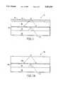
- FIG. 1is a schematic cross-sectional view of a portion of an X-ray image capture element in accordance with the present invention.
- FIG. 1ais a schematic cross-sectional view of a portion of an X-ray image capture element in accordance with an alternate embodiment of the present invention.
- FIG. 2is a schematic cross-sectional view of an electrical charge detecting array.
- FIG. 3is a schematic top view of an electrical charge detecting array in accordance with the present invention.
- FIG. 4is a schematic top view of the X-ray image capture element in accordance with the present invention.
- FIG. 5is a perspective view of an electronic cassette containing an X-ray image capture element in accordance with the present invention.
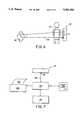
- FIG. 6is an elevation view of an arrangement for using an X-ray image capture element in accordance with the present invention.
- FIG. 7is a block diagram of an arrangement for the capture and display of a radiogram using an X-ray image capture element in accordance with the present invention.
- FIG. 1shows an image capture element 9 that is capable of convening a pattern of imagewise modulated radiation into a plurality of electrical charges representative of the imagewise modulated radiation.
- at least two adjoining array modules 17, which detect electrical chargesare contiguously positioned onto a base plate 13 to form the image capture element 9.
- the base plate 13is formed, for example, from a glass plate or composite material such as ceramic or carbon fiber laminates.
- the array modules 17are positioned such that a butt joint 12 is provided between adjacent edges of the two juxtaposed array modules 17.
- Each array module 17comprises a dielectric substrate 15 having at least two beveled edges, a plurality of transistor-capacitor pixels 19, and electronic addressing mid read-out means described later in more detail.
- the term pixelis used herein to define the smallest resolvable portion of the radiation pattern.
- the dielectric substrates 15 upon which the transistor-capacitor pixels 19 are to be fabricatedare processed as follows. Two sides, adjacent to a corner, of each substrate 15 are precision ground to a 90-degree ⁇ 4 seconds intersecting angle. The edges of each substrate 15 are ground to a 90-degree ⁇ 4 seconds angle perpendicular to the top surface. A 30 degree bevel is ground on the bottom of each substrate 15 along the edges where the substrates 15 are to be butted together to reduce the surface area of contact between substrates 15. All mating edges are lapped together using a 40 micron lapping compound, tier example, Micro-Grit.
- a key feature of the present inventionis a continuous radiation detecting material layer 14 formed over the plurality of array modules 17 to provide a singular, continuous means to detect incident X-ray radiation.
- the continuous nature of this layereliminates all non-radiation-detection or blind areas created in previous large area solid state detector arrays by borders of non-radiation-sensitive material, and also eliminates the need to overlay non-radiation-detection areas with additional radiation detectors by a tiling or shingle scheme.
- the radiation detecting layer 14is a photoconductive material which exhibits very high dark resistivity and may comprise any material exhibiting photoconductivity, meaning that upon exposure to X-radiation, the photoconductive material exhibit reduced resistivity relative to that in the absence of such exposure.
- the specific type of radiation detecting material selectedwill further depend upon the desired charge generation efficiency and charge transport property, and the desired simplicity of manufacture.
- Seleniumis one preferred material although cadmium sulfide, mercuric iodide, or lead oxide could be used.
- FIG. 1ashows an alternate embodiment of the present invention wherein the radiation detecting layer 14a is chosen to be a scintillating material, the scintillating material converting incident radiation into visible light to detect the radiation pattern, the pattern then being converted in this embodiment into a plurality of electrical charges by means of a transistor-photodiode pixel 19a.
- a plurality of transistor-photodiode pixels 19aare employed in place of the above described transistor-capacitor pixels 19.
- the photodiodesare formed using a layer of amorphous or polycrystalline silicon deposited between p-doped and n-doped layers of amorphous silicon.
- Typical thicknesses of the charge-doped layersare 25-100 nanometers, and the amorphous or polycrystalline silicon layer is typically one micron, a thickness capable of absorbing all the photons generated within the scintillating material layer 14a.
- thicknesses of the various layers in the photodiodecan be adjusted to maximum electrical charge capture, depending on the spectral emission wavelength of the scintillating radiation detecting material.
- a further deposition of conductive material that is transparent to X-rays, preferably indium-tin-oxide,is useful in enabling electrical readout.
- the scintillating radiation detecting materialis preferably chosen from the group consisting of gadolinium oxysulfide, calcium tungstate.
- Typical thickness of the radiation detecting layer 14ais 500 microns, and this material is applied at a density of no more than 5.3 g/cm 3 , by means of wet chemical coating techniques, preferably blade coating.
- the scintillating radiation detecting materialis dispersed in suitable binder, chosen to not deleteriously absorb light emitted from the binder.
- Such bindersinclude polyvinyl butyral, a sodium o-sulfobenzaldehyde acetal of polyvinyl alcohol, and polyurethane elastomers.
- One preferred bindercomprises copolymers of alkyl acrylates and methacrylates with acrylic and methacrylic acid.
- the radiation detecting layer 14is applied over the plurality of array modules 17, using vapor deposition techniques, in sufficient thickness to absorb the incident X-radiation, or a substantial portion thereof to provide high efficiency in radiation detection.
- a partially crystallized selenium-arsenic alloy having about 1 percent by weight arsenicis preferably used to produce uniform layer thickness, although an amorphous alloy cart also be used.
- No adhesion layeris employed between the array modules 17 and the deposited selenium layer, the selenium layer being deposited until a thickness on the order of 150 to 400 micrometers is achieved.
- a dielectric layer 16is added on the top surface of the detecting layer 14 opposite the array modules 17, preferably using a lamination and uv-curable adhesive or wet coating process such as spin, dip or blade coating.
- the dielectric layer 16comprises a layer of polyethylene terephalate (Mylar®) having a thickness greater than 10 microns, as this material has been found to be well-suited for the lamination process.
- polyquinoloneis a preferable material.
- a final top layer 81 of conductive materialsuch as indium-tin oxide, aluminum, gold, copper, or any other conductive material that is substantially transparent to X-radiation is formed over the dielectric layer 16, using well known sputtering or vapor deposition techniques.
- FIG. 2shows a single transistor-capacitor pixel 19 from among the plurality of such pixels positioned over the dielectric substrate 15.
- the capacitor of each pixel 19, shown schematically in FIG. 3 as item 8,is formed from a plurality of discrete minute conductive outer microplates 18n (i.e., 18a, 18b, 18c, . . . 18n), preferably made of aluminum having dimensions that define the aforementioned pixel, the smallest picture element resolvable by the transistor-capacitor pixel 19.
- Each microplate 18nis connected to electrical ground by conductive lines not shown.
- a capacitive dielectric material 59such as silicon dioxide or silicon nitride.
- a plurality of inner microplates 4ni.e., 4a, 4b, 4c, . . . 4n
- a charge blocking layer 10typically aluminum oxide when the inner microplate 4n is made of aluminum, is provided over the top surface of the inner microplates 4n.
- the combination of layers 4n, 10, and 14behaves as a blocking diode, inhibiting one type of charge flow in one direction.
- the charge blocking layer 10must have sufficient thickness to prevent charge leakage, typically greater than 100 Angstroms.
- FIG. 3shows conductive electrodes or X1, X2, . . . Xn address lines 11 and conductive electrodes or Y1, Y2, . . . Yn sense lines 13 laid out generally orthogonally to each other in the spaces between the transistor-capacitor pixels 19.
- the Xn address lines 11are individually accessible through leads or connectors not specifically illustrated in the drawings, along the sides or edges of the array 17.
- Each Yn line 13is also connected to a charge amplifying detector 36 which produces a voltage output proportional to such charge.
- the technology to sample sequentially the output of the charge amplifying detectors to obtain an output signal, and the technology to form the charge amplifying detectorsare well known in the art.
- FIG. 3further shows a transistor 5 connecting each microplate 4n to an Xn line 11.
- Each transistor 5,typically comprises a field-effect transistor, FET, preferably having a hydrogenated amorphous-silicon layer 6, an insulating layer 99, a gate 55 connected to Xn address lines 11, and the two conductive electrodes, one electrode 53, the drain of the transistor, being connected to the Yn sense lines 13 and the other electrode 54, the source of the transistor, being connected to the inner microplates 4n.
- the transistors 5serve as bi-directional switches allowing current flow between the Yn sense lines 13 and the charge storage capacitors 8 depending on whether a bias voltage is applied to gate 55 through Xn address lines 11.
- the transistor 5could be formed using polycrystalline silicon, crystalline silicon or cadmium selenide for its semiconducting material layer 6, and is covered with a passivation layer 98 and shielded from low-energy radiation using dielectric substrate layer 15 or by using additional layers.
- low-energy radiationmeans ultraviolet, infrared, or visible radiation, but excludes X-radiation and gamma-radiation.
- the technology for the creation of the transistors 5, charge storage capacitors 8, photodiodes, inner microplates 4n and outer microplates 18nis well known in the art, and is also described for instance in "Modular Series on Solid State Devices," Volume 5 of Introduction to Microelectronics Fabrication by R. C. Jaeger, Published by Addison-Wesley in 1988.
- FIG. 4shows four array modules 17 positioned together to form a larger image capture element 9. Using this approach, four 7 ⁇ 8.5 inch arrays, for example, are combined to produce a single 14 ⁇ 17 inch image capture element 9.
- transistor-capacitor pixels 19are shown near the intersection of the array modules 17. In the instance that a single row of transistor-capacitor pixels 19 is effectively eliminated by the abutment process, that row of radiation pattern information is replaced by interpolation from the adjacent unaffected rows of transistor-capacitor pixels 19. This information loss is constrained to be no more than a single row of transistor-capacitor pixels 19 because of the combination of physical size of the transistor-capacitor pixel 19 and the precision lapping of the array substrates 15.
- the radiation detecting layeris discontinuous and, as a consequence of Feathering of the radiation detection layer at the abutting edges of the arrays, more than a single row of radiation pattern information will be missing.
- Linear interpolationis preferably used, however, other methods are also applicable.
- Electronic addressing means 44 for the array modules 17are separate for each of the modules 17, and these electronic means 44 address each of the individual transistor-capacitor pixels 19 and are electronically connected over lines 43 to a central control unit 42.
- the control unit 42enables sequential electronic access to the gates of the transistor-capacitor pixels 19 and simultaneous electronic access to the array modules 17, thus reducing readout time.
- Electronic signal readout means 41are connected to the transistor-capacitor pixels 19 and also to a multiplexing module 40 over lines 45.
- the multiplexing module 40is also connected to the central control unit 42 which provides control signals to the transistor-capacitor pixels 19 and receives electronic signals indicative of the strength of an incident imagewise-modulated X-ray pattern from each of the charge storage capacitors 8. If more than four array modules are needed to be assembled in abutting fashion, it is necessary to change the electronic addressing means from one using connections made at the outer edges of the array modules in order to access the innermost array modules, for instance the 2 inner array modules in a pattern of six array modules. In this situation, through-hole, or via interconnections are made at the edges of the inner arrays, the vias extending to the bottom of the substrates 15 and exiting at the electrically accessible back side of the image element 9.
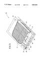
- FIG. 5shows the essential features of an electronic cassette 20 formed by front and back members 23 and 24, respectively, that would typically be used to house an X-ray image capture element 9 comprising, for example, four array modules 17.
- the central control unit 42causes power from a power supply 38 to be supplied to the X-ray image capture element 9 and also activates all the addressing electronics 44 and readout electronics 41 associated with the X-ray image capture element 9.
- the impinging radiationis converted to a plurality of electrical charges by the X-ray image capture element 9.
- X-ray sensor 58senses presence of X-radiation followed by absence of X-radiation, a process of digitizing the plurality of electrical charges begins within the X-ray-image capture element 9.
- This plurality of chargesis converted within the readout electronics 41 to produce a plurality of digitized image element values, and these values are transferred to electronic memory storage means 35 which could be solid-state memory circuits or a miniature magnetic or optical digital recorder located within the electronic cassette 20.
- electronic memory storage means 35which could be solid-state memory circuits or a miniature magnetic or optical digital recorder located within the electronic cassette 20.
- the digitized image element valuesare directed to the central control unit 42 and then to connector 28 on the electronic cassette 20. After the digitized image element values are stored in memory, central control unit 42 causes the image capture element 9 to be erased in preparation for capturing a subsequent radiogram.
- FIG. 6shows the image capture element 9 in its process of use.
- Electronic cassette 20 containing image capture element 9is placed by an operator, generally a medical technician, in a first position much like a standard screen-film cassette is used to receive a first imagewise modulated X-ray pattern.
- a target 61i.e., a patient in the case of medical diagnostic imaging, is positioned in an X-ray beam path 65 emitted by a source of X-radiation 63.
- the radiation emerging through the target 61is imagewise modulated in intensity because of the different degree of X-ray absorption in the target 61 and the pattern of this imagewise modulated radiation is captured and stored by image capture element 9 contained in the electronic cassette 20.
- FIG. 7shows the digitized picture element values obtained from the electronic cassette 20 using connector 28 and directed to an external computer 144 via line 140.
- Computer 144directs the signal to appropriate storage means which may be either an internal RAM memory within a host computer or a long term archive memory 142 or both.
- image processingsuch as filtering, contrast enhancement by many different external systems for permanently recording digital data, modifying the data to facilitate interpretation and reconstructing the digitized picture element values into visible images, and may be displayed on a CRT 146 for immediate viewing or used in a printer 148 to produce a hard copy 150, or sent to a remote reading location by means of teleradiography.
Landscapes
- Engineering & Computer Science (AREA)
- Multimedia (AREA)
- Signal Processing (AREA)
- Measurement Of Radiation (AREA)
- Solid State Image Pick-Up Elements (AREA)
- Image-Pickup Tubes, Image-Amplification Tubes, And Storage Tubes (AREA)
- Electroluminescent Light Sources (AREA)
- Thin Film Transistor (AREA)
- Light Receiving Elements (AREA)
Abstract
Description
Claims (20)
Priority Applications (3)
| Application Number | Priority Date | Filing Date | Title |
|---|---|---|---|
| US08174861US5381014B1 (en) | 1993-12-29 | 1993-12-29 | Large area x-ray imager and method of fabrication |
| EP94119282AEP0661556A3 (en) | 1993-12-29 | 1994-12-07 | Large x-ray generator and method of its production. |
| JP6328814AJPH07235652A (en) | 1993-12-29 | 1994-12-28 | X-ray image capturing element and manufacturing method thereof |
Applications Claiming Priority (1)
| Application Number | Priority Date | Filing Date | Title |
|---|---|---|---|
| US08174861US5381014B1 (en) | 1993-12-29 | 1993-12-29 | Large area x-ray imager and method of fabrication |
Publications (2)
| Publication Number | Publication Date |
|---|---|
| US5381014Atrue US5381014A (en) | 1995-01-10 |
| US5381014B1 US5381014B1 (en) | 1997-06-10 |
Family
ID=22637834
Family Applications (1)
| Application Number | Title | Priority Date | Filing Date |
|---|---|---|---|
| US08174861Expired - Fee RelatedUS5381014B1 (en) | 1993-12-29 | 1993-12-29 | Large area x-ray imager and method of fabrication |
Country Status (3)
| Country | Link |
|---|---|
| US (1) | US5381014B1 (en) |
| EP (1) | EP0661556A3 (en) |
| JP (1) | JPH07235652A (en) |
Cited By (89)
| Publication number | Priority date | Publication date | Assignee | Title |
|---|---|---|---|---|
| US5440146A (en)* | 1994-03-31 | 1995-08-08 | Minnesota Mining And Manufacturing Company | Radiographic image reader |
| WO1997005658A1 (en)* | 1995-07-31 | 1997-02-13 | Litton Systems Canada Limited | Flat panel detector for radiation imaging and pixel for use therein |
| US5608245A (en)* | 1995-12-21 | 1997-03-04 | Xerox Corporation | Array on substrate with repair line crossing lines in the array |
| WO1997010616A1 (en)* | 1995-09-12 | 1997-03-20 | Philips Electronics N.V. | X-ray image sensor |
| US5619033A (en)* | 1995-06-07 | 1997-04-08 | Xerox Corporation | Layered solid state photodiode sensor array |
| US5648674A (en)* | 1995-06-07 | 1997-07-15 | Xerox Corporation | Array circuitry with conductive lines, contact leads, and storage capacitor electrode all formed in layer that includes highly conductive metal |
| US5650626A (en)* | 1996-07-16 | 1997-07-22 | Eastman Kodak Company | X-ray imaging detector with thickness and composition limited substrate |
| US5652430A (en)* | 1996-05-03 | 1997-07-29 | Sterling Diagnostic Imaging, Inc. | Direct radiographic imaging panel |
| US5658186A (en)* | 1996-07-16 | 1997-08-19 | Sterling Diagnostic Imaging, Inc. | Jig for polishing the edge of a thin solid state array panel |
| US5693947A (en)* | 1993-04-28 | 1997-12-02 | The University Of Surrey | Radiation detectors |
| US5693567A (en)* | 1995-06-07 | 1997-12-02 | Xerox Corporation | Separately etching insulating layer for contacts within array and for peripheral pads |
| WO1998002922A1 (en)* | 1996-07-16 | 1998-01-22 | Sterling Diagnostic Imaging Incorporated | Fabrication of large area x-ray image capturing element |
| US5731803A (en)* | 1995-12-21 | 1998-03-24 | Xerox Corporation | Array with light active units sized to eliminate artifact from size difference |
| WO1998018166A1 (en)* | 1996-10-18 | 1998-04-30 | Simage Oy | Imaging detector and method of production |
| DE19644936A1 (en)* | 1996-10-29 | 1998-05-07 | Geesthacht Gkss Forschung | Element analysis arrangement for material using X-ray fluorescence |
| US5753921A (en)* | 1996-07-16 | 1998-05-19 | Eastman Kodak Company | X-ray imaging detector with limited substrate and converter |
| US5773839A (en)* | 1994-03-31 | 1998-06-30 | Imation Corp. | Cassette for use in an electronic radiographic imaging system |
| WO1998032179A1 (en)* | 1997-01-21 | 1998-07-23 | Thomson Tubes Electroniques | Method for tight sealing of a radiation detector and detector obtained by this method |
| WO1998032180A1 (en)* | 1997-01-21 | 1998-07-23 | Thomson Tubes Electroniques | Method for producing a radiation detector by assembling elementary blocks and resulting detector |
| FR2758655A1 (en)* | 1997-01-21 | 1998-07-24 | Thomson Tubes Electroniques | METHOD FOR PRODUCING A RADIOGRAPHY DETECTOR BY ASSEMBLY OF ELEMENTARY SLABS AND DETECTOR THUS OBTAINED |
| FR2758654A1 (en)* | 1997-01-21 | 1998-07-24 | Thomson Tubes Electroniques | Large flat screen radiation detector production |
| FR2758679A1 (en)* | 1997-01-21 | 1998-07-24 | Thomson Tubes Electroniques | Solid-state, large-scale X-ray detector with scintillator array |
| US5804832A (en)* | 1996-11-26 | 1998-09-08 | Sterling Diagnostic Imaging, Inc. | Digital array for radiographic imaging |
| US5818053A (en)* | 1992-02-20 | 1998-10-06 | Imation Corp. | Multi-module solid state radiation detector with continuous photoconductor layer and fabrication method |
| US5844243A (en)* | 1997-07-15 | 1998-12-01 | Direct Radiography Co. | Method for preparing digital radiography panels |
| US5917199A (en)* | 1998-05-15 | 1999-06-29 | Ois Optical Imaging Systems, Inc. | Solid state imager including TFTS with variably doped contact layer system for reducing TFT leakage current and increasing mobility and method of making same |
| US5973311A (en)* | 1997-02-12 | 1999-10-26 | Imation Corp | Pixel array with high and low resolution mode |
| US6013916A (en)* | 1997-07-23 | 2000-01-11 | The Regents Of The University Of Michigan | Flat panel dosimeter |
| WO2000002258A1 (en)* | 1998-07-07 | 2000-01-13 | Direct Radiography Corp. | Large area x-ray imager with vented seam and method of fabrication |
| US6025599A (en)* | 1997-12-09 | 2000-02-15 | Direct Radiography Corp. | Image capture element |
| US6060683A (en)* | 1998-09-22 | 2000-05-09 | Direct Radiography Corp. | Selective laser removal of dielectric coating |
| US6060714A (en)* | 1998-01-23 | 2000-05-09 | Ois Optical Imaging Systems, Inc. | Large area imager with photo-imageable interface barrier layer |
| US6075248A (en)* | 1998-10-22 | 2000-06-13 | Direct Radiography Corp. | Direct radiographic imaging panel with shielding electrode |
| EP1018768A1 (en) | 1999-01-05 | 2000-07-12 | Direct Radiography Corp. | Image capture element |
| EP0933650A3 (en)* | 1998-01-28 | 2000-08-02 | Canon Kabushiki Kaisha | Two-dimensional image pickup apparatus |
| EP1049170A1 (en)* | 1999-04-30 | 2000-11-02 | Commissariat A L'energie Atomique | Miniaturised gamma camera with semiconductor detectors |
| FR2793072A1 (en)* | 1999-04-30 | 2000-11-03 | Commissariat Energie Atomique | COMPACT DETECTION DEVICE FOR GAMMA CAMERA |
| US6194727B1 (en) | 1998-07-06 | 2001-02-27 | Direct Radiography Corp. | Direct radiographic imaging panel having a dielectric layer with an adjusted time constant |
| JP3183390B2 (en) | 1995-09-05 | 2001-07-09 | キヤノン株式会社 | Photoelectric conversion device and imaging device using the same |
| WO2001050155A1 (en)* | 1999-12-29 | 2001-07-12 | Xcounter Ab | A method and an apparatus for radiography and a radiation detector |
| US6281507B1 (en) | 1999-06-30 | 2001-08-28 | Siemens Medical Systems, Inc. | Interdigital photoconductor structure for direct X-ray detection in a radiography imaging system |
| US20010041832A1 (en)* | 2000-03-31 | 2001-11-15 | Akira Hirai | Imaging apparatus, imaging system, imaging control method, and storage medium |
| US6335796B1 (en) | 1996-12-20 | 2002-01-01 | Canon Kabushiki Kaisha | Image pick-up apparatus, image pick-up method, and image pick-up system |
| US20020014594A1 (en)* | 2000-06-27 | 2002-02-07 | Takashi Endo | Radiation imaging system |
| US6350985B1 (en) | 1999-04-26 | 2002-02-26 | Direct Radiography Corp. | Method for calculating gain correction factors in a digital imaging system |
| US6400428B1 (en)* | 1995-04-14 | 2002-06-04 | Sharp Kabushiki Kaisha | Liquid crystal device/display utilizing a plurality of adjoining display panels to form single display screen and methods related thereto |
| US6403964B1 (en)* | 1997-12-18 | 2002-06-11 | Simage Oy | Modular imaging apparatus |
| US6405068B1 (en) | 1997-02-04 | 2002-06-11 | Osteometer Meditech A/S | Diagnostic imaging in relation to arthritic conditions |
| US6429414B1 (en)* | 1999-03-31 | 2002-08-06 | Siemens Aktiengesellschaft | Solid state image detector and method for producing same |
| US20020196899A1 (en)* | 1989-12-05 | 2002-12-26 | University Of Massachusetts Medical Center | System for quantitative radiographic imaging |
| US6510202B2 (en) | 2000-03-31 | 2003-01-21 | Canon Kabushiki Kaisha | Imaging apparatus, imaging method, and storage medium |
| US6512279B2 (en)* | 1993-12-27 | 2003-01-28 | Canon Kabushiki Kaisha | Photoelectric converter, its driving method, and system including the photoelectric converter |
| US6516098B2 (en) | 1997-11-20 | 2003-02-04 | Canon Kabushiki Kaisha | Apparatus and method of obtaining a radiation image of an object |
| US6600160B2 (en) | 1998-02-20 | 2003-07-29 | Canon Kabushiki Kaisha | Photoelectric converter and radiation reader |
| US20030169847A1 (en)* | 2001-11-21 | 2003-09-11 | University Of Massachusetts Medical Center | System and method for x-ray fluoroscopic imaging |
| EP0997949A3 (en)* | 1998-10-28 | 2004-02-25 | Canon Kabushiki Kaisha | Image pick-up apparatus and image pick-up system, and method for manufacturing image pick-up apparatus |
| EP1432043A2 (en) | 1997-04-10 | 2004-06-23 | Canon Kabushiki Kaisha | Photoelectric conversion apparatus |
| US20040123953A1 (en)* | 2001-06-25 | 2004-07-01 | Emanuel Beer | Apparatus and method for thermally isolating a heat chamber |
| US6819786B2 (en) | 2000-04-06 | 2004-11-16 | Canon Kabushiki Kaisha | Image processing apparatus |
| US20050047639A1 (en)* | 2003-08-26 | 2005-03-03 | Shinsuke Hayashida | Radiographic apparatus and radiographic method |
| US20050056789A1 (en)* | 2003-09-12 | 2005-03-17 | Martin Spahn | X-ray detector |
| JP2005260249A (en)* | 1995-09-05 | 2005-09-22 | Canon Inc | Photoelectric conversion device and radiation imaging device |
| US20050205797A1 (en)* | 2001-02-07 | 2005-09-22 | Canon Kabushiki Kaisha | Scintillator panel, method of manufacturing scintillator panel, radiation detection device, and radiation detection system |
| US20060065842A1 (en)* | 2003-02-27 | 2006-03-30 | Kabushiki Kaisha Toshiba | X-ray detector and x-ray examination device using it |
| US20060165214A1 (en)* | 2003-01-06 | 2006-07-27 | Mattson Rodney A | Radiation detector with shielded electronics for computed tomography |
| DE102005036811A1 (en)* | 2005-08-04 | 2007-02-08 | Siemens Ag | Correction method for digital solid detector, involves correcting and removing discontinuities produced on digital Roentgen unprocessed image due to transfer of plates of pixel matrix of solid detector |
| US20070045547A1 (en)* | 1996-02-02 | 2007-03-01 | Tumer Tumay O | Method and apparatus for radiation detection |
| US20070051894A1 (en)* | 2003-12-10 | 2007-03-08 | Koninklijke Philips Electronic, N.V. | X-ray detector |
| JP2009246378A (en)* | 1995-09-05 | 2009-10-22 | Canon Inc | Photoelectric converter, and radiation imaging apparatus |
| FR2945354A1 (en)* | 2009-05-11 | 2010-11-12 | Gen Electric | DIGITAL IMAGE DETECTOR |
| CN102466808A (en)* | 2010-11-09 | 2012-05-23 | 北京大基康明医疗设备有限公司 | Amorphous silicon cesium iodide digital X-ray flat panel detector |
| US20120228505A1 (en)* | 2011-03-09 | 2012-09-13 | Samsung Electronics Co., Ltd. | Optical sensor |
| US8356758B1 (en) | 2012-04-25 | 2013-01-22 | Eastman Kodak Company | Making storage system having modifiable conductor and memory |
| US8383443B2 (en) | 2010-05-14 | 2013-02-26 | International Business Machines Corporation | Non-uniform gate dielectric charge for pixel sensor cells and methods of manufacturing |
| US8445853B2 (en) | 2011-08-22 | 2013-05-21 | Eastman Kodak Company | Method of making a radiation-sensitive substrate |
| US8530848B2 (en) | 2011-08-22 | 2013-09-10 | Eastman Kodak Company | Radiation-sensitive substrate |
| US20140133637A1 (en)* | 2012-11-09 | 2014-05-15 | Canon Kabushiki Kaisha | Image processing apparatus, image processing method, radiation imaging system, and storage medium |
| US8739399B2 (en) | 2012-04-25 | 2014-06-03 | Eastman Kodak Company | Making electronic storage system having code circuit |
| US8745861B2 (en) | 2012-04-25 | 2014-06-10 | Eastman Kodak Company | Method of making a storage system having an environmentally-modifiable conductor |
| CN105829916A (en)* | 2013-12-13 | 2016-08-03 | 佳能株式会社 | Radiation detection device, radiation detection system, and method for manufacturing a radiation detection device |
| US20170133428A1 (en)* | 2015-06-29 | 2017-05-11 | Boe Technology Group Co., Ltd. | Radiographic detection substrate and manufacture method thereof, radiographic detection device |
| US9808159B2 (en) | 2013-05-08 | 2017-11-07 | Makoto Shizukuishi | Solid-state image sensor and imaging apparatus including the same |
| US9917133B2 (en) | 2013-12-12 | 2018-03-13 | General Electric Company | Optoelectronic device with flexible substrate |
| US9935152B2 (en) | 2012-12-27 | 2018-04-03 | General Electric Company | X-ray detector having improved noise performance |
| DE102015213911B4 (en) | 2015-07-23 | 2019-03-07 | Siemens Healthcare Gmbh | Method for generating an X-ray image and data processing device for carrying out the method |
| US10732131B2 (en) | 2014-03-13 | 2020-08-04 | General Electric Company | Curved digital X-ray detector for weld inspection |
| US11504079B2 (en) | 2016-11-30 | 2022-11-22 | The Research Foundation For The State University Of New York | Hybrid active matrix flat panel detector system and method |
| US20230266488A1 (en)* | 2022-02-22 | 2023-08-24 | KETEK GmbH Halbleiter- und Reinraumtechnik | X-Ray Radiation Detector and Operation Method |
| US12029691B2 (en) | 2019-07-09 | 2024-07-09 | Makoto Shizukuishi | Medical vehicles, CT devices, and driving method |
Families Citing this family (4)
| Publication number | Priority date | Publication date | Assignee | Title |
|---|---|---|---|---|
| TW331667B (en)* | 1995-09-05 | 1998-05-11 | Canon Kk | Photoelectric converter |
| JP2000077640A (en)* | 1998-06-19 | 2000-03-14 | Canon Inc | Image reading device and radiation imaging device |
| KR100463337B1 (en)* | 1998-09-16 | 2005-06-08 | 엘지.필립스 엘시디 주식회사 | X-ray image sensor and mothed for fabricating the same |
| JP6077787B2 (en)* | 2012-08-22 | 2017-02-08 | キヤノン株式会社 | Radiation imaging apparatus and radiation imaging system |
Citations (27)
| Publication number | Priority date | Publication date | Assignee | Title |
|---|---|---|---|---|
| US3973146A (en)* | 1974-03-18 | 1976-08-03 | North American Philips Corporation | Signal detector comprising field effect transistors |
| US4467342A (en)* | 1982-07-15 | 1984-08-21 | Rca Corporation | Multi-chip imager |
| EP0125691A2 (en)* | 1983-05-16 | 1984-11-21 | Fuji Photo Film Co., Ltd. | Method for dectecting radiation image |
| US4670765A (en)* | 1984-04-02 | 1987-06-02 | Sharp Kabushiki Kaisha | Semiconductor photodetector element |
| US4672454A (en)* | 1984-05-04 | 1987-06-09 | Energy Conversion Devices, Inc. | X-ray image scanner and method |
| US4694317A (en)* | 1984-10-22 | 1987-09-15 | Fuji Photo Film Co., Ltd. | Solid state imaging device and process for fabricating the same |
| JPS633454A (en)* | 1986-06-24 | 1988-01-08 | Seiko Epson Corp | Solid-state image sensing device and manufacture thereof |
| US4755681A (en)* | 1986-09-30 | 1988-07-05 | Shimadzu Corporation | Radiation image detecting apparatus with IC modules stacked stepwise |
| US4770965A (en)* | 1986-12-23 | 1988-09-13 | Xerox Corporation | Selenium alloy imaging member |
| US4810881A (en)* | 1986-04-30 | 1989-03-07 | Thomson-Csf | Panel for X-ray photography and method of manufacture |
| US4857723A (en)* | 1987-09-14 | 1989-08-15 | Texas Medical Instruments, Inc. | Segmented imaging plate structure |
| US4861995A (en)* | 1987-03-24 | 1989-08-29 | Fuji Photo Film Co., Ltd. | Radiation image read-out apparatus |
| US4873708A (en)* | 1987-05-11 | 1989-10-10 | General Electric Company | Digital radiographic imaging system and method therefor |
| US4931643A (en)* | 1987-11-17 | 1990-06-05 | Siemens Aktiengesellschaft | Autoradiography system for stimulable phosphor foils |
| US4961209A (en)* | 1987-12-01 | 1990-10-02 | Noranda, Inc. | System for measuring the charge distribution on a photoreceptor surface |
| US4975935A (en)* | 1988-12-17 | 1990-12-04 | U.S. Philips Corporation | Method of producing an X-ray exposure by means of a photoconductor and arrangement for carrying out the method |
| US5043582A (en)* | 1985-12-11 | 1991-08-27 | General Imagining Corporation | X-ray imaging system and solid state detector therefor |
| US5070248A (en)* | 1989-07-12 | 1991-12-03 | Minnesota Mining And Manufacturing Company | Cassette with intensifying screens to be used with an x-ray film |
| US5105087A (en)* | 1990-11-28 | 1992-04-14 | Eastman Kodak Company | Large solid state sensor assembly formed from smaller sensors |
| US5127038A (en)* | 1991-06-28 | 1992-06-30 | E. I. Du Pont De Nemours And Company | Method for capturing and displaying a latent radiographic image |
| US5151588A (en)* | 1989-11-24 | 1992-09-29 | Shimadzu Corporation | Radiation imaging apparatus having detection elements of varying sizes |
| US5166524A (en)* | 1991-06-28 | 1992-11-24 | E. I. Du Pont De Nemours & Company | Element, device and associated method for capturing a latent radiographic image |
| US5182624A (en)* | 1990-08-08 | 1993-01-26 | Minnesota Mining And Manufacturing Company | Solid state electromagnetic radiation detector fet array |
| US5220170A (en)* | 1985-12-11 | 1993-06-15 | General Imaging Corporation | X-ray imaging system and solid state detector therefor |
| US5254480A (en)* | 1992-02-20 | 1993-10-19 | Minnesota Mining And Manufacturing Company | Process for producing a large area solid state radiation detector |
| US5315101A (en)* | 1992-02-08 | 1994-05-24 | U.S. Philips Corporation | Method of manufacturing a large area active matrix array |
| US5319206A (en)* | 1992-12-16 | 1994-06-07 | E. I. Du Pont De Nemours And Company | Method and apparatus for acquiring an X-ray image using a solid state device |
- 1993
- 1993-12-29USUS08174861patent/US5381014B1/ennot_activeExpired - Fee Related
- 1994
- 1994-12-07EPEP94119282Apatent/EP0661556A3/ennot_activeCeased
- 1994-12-28JPJP6328814Apatent/JPH07235652A/enactivePending
Patent Citations (28)
| Publication number | Priority date | Publication date | Assignee | Title |
|---|---|---|---|---|
| US3973146A (en)* | 1974-03-18 | 1976-08-03 | North American Philips Corporation | Signal detector comprising field effect transistors |
| US4467342A (en)* | 1982-07-15 | 1984-08-21 | Rca Corporation | Multi-chip imager |
| EP0125691A2 (en)* | 1983-05-16 | 1984-11-21 | Fuji Photo Film Co., Ltd. | Method for dectecting radiation image |
| US4803359A (en)* | 1983-05-16 | 1989-02-07 | Fuji Photo Film Co., Ltd. | Method for detecting radiation image |
| US4670765A (en)* | 1984-04-02 | 1987-06-02 | Sharp Kabushiki Kaisha | Semiconductor photodetector element |
| US4672454A (en)* | 1984-05-04 | 1987-06-09 | Energy Conversion Devices, Inc. | X-ray image scanner and method |
| US4694317A (en)* | 1984-10-22 | 1987-09-15 | Fuji Photo Film Co., Ltd. | Solid state imaging device and process for fabricating the same |
| US5043582A (en)* | 1985-12-11 | 1991-08-27 | General Imagining Corporation | X-ray imaging system and solid state detector therefor |
| US5220170A (en)* | 1985-12-11 | 1993-06-15 | General Imaging Corporation | X-ray imaging system and solid state detector therefor |
| US4810881A (en)* | 1986-04-30 | 1989-03-07 | Thomson-Csf | Panel for X-ray photography and method of manufacture |
| JPS633454A (en)* | 1986-06-24 | 1988-01-08 | Seiko Epson Corp | Solid-state image sensing device and manufacture thereof |
| US4755681A (en)* | 1986-09-30 | 1988-07-05 | Shimadzu Corporation | Radiation image detecting apparatus with IC modules stacked stepwise |
| US4770965A (en)* | 1986-12-23 | 1988-09-13 | Xerox Corporation | Selenium alloy imaging member |
| US4861995A (en)* | 1987-03-24 | 1989-08-29 | Fuji Photo Film Co., Ltd. | Radiation image read-out apparatus |
| US4873708A (en)* | 1987-05-11 | 1989-10-10 | General Electric Company | Digital radiographic imaging system and method therefor |
| US4857723A (en)* | 1987-09-14 | 1989-08-15 | Texas Medical Instruments, Inc. | Segmented imaging plate structure |
| US4931643A (en)* | 1987-11-17 | 1990-06-05 | Siemens Aktiengesellschaft | Autoradiography system for stimulable phosphor foils |
| US4961209A (en)* | 1987-12-01 | 1990-10-02 | Noranda, Inc. | System for measuring the charge distribution on a photoreceptor surface |
| US4975935A (en)* | 1988-12-17 | 1990-12-04 | U.S. Philips Corporation | Method of producing an X-ray exposure by means of a photoconductor and arrangement for carrying out the method |
| US5070248A (en)* | 1989-07-12 | 1991-12-03 | Minnesota Mining And Manufacturing Company | Cassette with intensifying screens to be used with an x-ray film |
| US5151588A (en)* | 1989-11-24 | 1992-09-29 | Shimadzu Corporation | Radiation imaging apparatus having detection elements of varying sizes |
| US5182624A (en)* | 1990-08-08 | 1993-01-26 | Minnesota Mining And Manufacturing Company | Solid state electromagnetic radiation detector fet array |
| US5105087A (en)* | 1990-11-28 | 1992-04-14 | Eastman Kodak Company | Large solid state sensor assembly formed from smaller sensors |
| US5127038A (en)* | 1991-06-28 | 1992-06-30 | E. I. Du Pont De Nemours And Company | Method for capturing and displaying a latent radiographic image |
| US5166524A (en)* | 1991-06-28 | 1992-11-24 | E. I. Du Pont De Nemours & Company | Element, device and associated method for capturing a latent radiographic image |
| US5315101A (en)* | 1992-02-08 | 1994-05-24 | U.S. Philips Corporation | Method of manufacturing a large area active matrix array |
| US5254480A (en)* | 1992-02-20 | 1993-10-19 | Minnesota Mining And Manufacturing Company | Process for producing a large area solid state radiation detector |
| US5319206A (en)* | 1992-12-16 | 1994-06-07 | E. I. Du Pont De Nemours And Company | Method and apparatus for acquiring an X-ray image using a solid state device |
Non-Patent Citations (10)
| Title |
|---|
| L. E. Antonuk et al., Development of Hydrogenated Amorphous Silicon Sensors For Diagnostic X Ray Imaging, IEEE Transactions on Nuclear Science , 38 , No. 2, 636 640, Apr. 1991.* |
| L. E. Antonuk et al., Development of Hydrogenated Amorphous Silicon Sensors For Diagnostic X-Ray Imaging, IEEE Transactions on Nuclear Science, 38 , No. 2, 636-640, Apr. 1991. |
| L. E. Antonuk et al., Development of Hydrogenated Amorphous Silicon Sensors For High Energy Photon Radiotherapy Imaging, IEEE Transactions on Nuclear Science , 37, No. 2, 165 170, Apr. 1990.* |
| L. E. Antonuk et al., Development of Hydrogenated Amorphous Silicon Sensors For High Energy Photon Radiotherapy Imaging, IEEE Transactions on Nuclear Science, 37, No. 2, 165-170, Apr. 1990. |
| L. E. Antonuk et al., Development of Thin Film, Flat Panel Arrays For Diagnostic and Radiotherapy Imaging, Conference Proceedings of SPIE Medical Imaging VI , Newport Beach, Calif., Feb. 23 27, 1992.* |
| L. E. Antonuk et al., Development of Thin-Film, Flat-Panel Arrays For Diagnostic and Radiotherapy Imaging, Conference Proceedings of SPIE Medical Imaging VI, Newport Beach, Calif., Feb. 23-27, 1992. |
| L. E. Antonuk et al., Large Area Amorphous Silicon Photodiode Arrays for Radiotherapy and Diagnostic Imaging, Nuclear Instruments and Methods in Physics Research , A310 (1991), pp. 460 464.* |
| L. E. Antonuk et al., Large Area Amorphous Silicon Photodiode Arrays for Radiotherapy and Diagnostic Imaging, Nuclear Instruments and Methods in Physics Research, A310 (1991), pp. 460-464. |
| L. E. Antonuk et al., Signal, Noise, and Readout Considerations in The Development of Amorphous Silicon Photodiode Arrays For Radiotherapy and Diagnostic X Ray Imaging, SPIE , 1443 Medical Imaging V: Image Physics, 108 119, (1991).* |
| L. E. Antonuk et al., Signal, Noise, and Readout Considerations in The Development of Amorphous Silicon Photodiode Arrays For Radiotherapy and Diagnostic X-Ray Imaging, SPIE, 1443 Medical Imaging V: Image Physics, 108-119, (1991). |
Cited By (151)
| Publication number | Priority date | Publication date | Assignee | Title |
|---|---|---|---|---|
| US20020196899A1 (en)* | 1989-12-05 | 2002-12-26 | University Of Massachusetts Medical Center | System for quantitative radiographic imaging |
| US5818053A (en)* | 1992-02-20 | 1998-10-06 | Imation Corp. | Multi-module solid state radiation detector with continuous photoconductor layer and fabrication method |
| US6262421B1 (en) | 1992-02-20 | 2001-07-17 | Imation Corp. | Solid state radiation detector for x-ray imaging |
| US5942756A (en)* | 1992-02-20 | 1999-08-24 | Imation Corp. | Radiation detector and fabrication method |
| US5693947A (en)* | 1993-04-28 | 1997-12-02 | The University Of Surrey | Radiation detectors |
| US6982422B2 (en) | 1993-12-27 | 2006-01-03 | Canon Kabushiki Kaisha | Photoelectric converter, its driving method, and system including the photoelectric converter |
| US7022997B2 (en) | 1993-12-27 | 2006-04-04 | Canon Kabushiki Kaisha | Photoelectric converter, its driving method, and system including the photoelectric converter |
| US20060027758A1 (en)* | 1993-12-27 | 2006-02-09 | Canon Kabushiki Kaisha | Photoelectric converter, its driving method, and system including the photoelectric converter |
| US6512279B2 (en)* | 1993-12-27 | 2003-01-28 | Canon Kabushiki Kaisha | Photoelectric converter, its driving method, and system including the photoelectric converter |
| US5440146A (en)* | 1994-03-31 | 1995-08-08 | Minnesota Mining And Manufacturing Company | Radiographic image reader |
| US5773839A (en)* | 1994-03-31 | 1998-06-30 | Imation Corp. | Cassette for use in an electronic radiographic imaging system |
| US6400428B1 (en)* | 1995-04-14 | 2002-06-04 | Sharp Kabushiki Kaisha | Liquid crystal device/display utilizing a plurality of adjoining display panels to form single display screen and methods related thereto |
| US7034906B2 (en) | 1995-04-14 | 2006-04-25 | Sharp Kabushiki Kaisha | Display device utilizing a plurality of adjoining display panels to form single display screen and methods related thereto |
| US7869569B2 (en) | 1995-05-11 | 2011-01-11 | University Of Massachusetts | System for quantitative radiographic imaging |
| US20080304620A1 (en)* | 1995-05-11 | 2008-12-11 | University Of Massachusetts | System for quantitative radiographic imaging |
| US5693567A (en)* | 1995-06-07 | 1997-12-02 | Xerox Corporation | Separately etching insulating layer for contacts within array and for peripheral pads |
| US5619033A (en)* | 1995-06-07 | 1997-04-08 | Xerox Corporation | Layered solid state photodiode sensor array |
| US5648674A (en)* | 1995-06-07 | 1997-07-15 | Xerox Corporation | Array circuitry with conductive lines, contact leads, and storage capacitor electrode all formed in layer that includes highly conductive metal |
| US6232606B1 (en) | 1995-07-31 | 2001-05-15 | Ifire Technology, Inc. | Flat panel detector for radiation imaging and pixel for use therein |
| WO1997005658A1 (en)* | 1995-07-31 | 1997-02-13 | Litton Systems Canada Limited | Flat panel detector for radiation imaging and pixel for use therein |
| JP2009246378A (en)* | 1995-09-05 | 2009-10-22 | Canon Inc | Photoelectric converter, and radiation imaging apparatus |
| JP3183390B2 (en) | 1995-09-05 | 2001-07-09 | キヤノン株式会社 | Photoelectric conversion device and imaging device using the same |
| JP2005260249A (en)* | 1995-09-05 | 2005-09-22 | Canon Inc | Photoelectric conversion device and radiation imaging device |
| WO1997010616A1 (en)* | 1995-09-12 | 1997-03-20 | Philips Electronics N.V. | X-ray image sensor |
| US5729021A (en)* | 1995-09-12 | 1998-03-17 | U.S. Philips Corporation | X-ray image sensor |
| US5731803A (en)* | 1995-12-21 | 1998-03-24 | Xerox Corporation | Array with light active units sized to eliminate artifact from size difference |
| US5608245A (en)* | 1995-12-21 | 1997-03-04 | Xerox Corporation | Array on substrate with repair line crossing lines in the array |
| US7566879B2 (en)* | 1996-02-02 | 2009-07-28 | Tuemer Tuemay O | Method and apparatus for radiation detection |
| US20100025592A1 (en)* | 1996-02-02 | 2010-02-04 | Tumay Tumer | Method and apparatus for radiation detection |
| US20070045547A1 (en)* | 1996-02-02 | 2007-03-01 | Tumer Tumay O | Method and apparatus for radiation detection |
| US5652430A (en)* | 1996-05-03 | 1997-07-29 | Sterling Diagnostic Imaging, Inc. | Direct radiographic imaging panel |
| US5753921A (en)* | 1996-07-16 | 1998-05-19 | Eastman Kodak Company | X-ray imaging detector with limited substrate and converter |
| US5650626A (en)* | 1996-07-16 | 1997-07-22 | Eastman Kodak Company | X-ray imaging detector with thickness and composition limited substrate |
| US5658186A (en)* | 1996-07-16 | 1997-08-19 | Sterling Diagnostic Imaging, Inc. | Jig for polishing the edge of a thin solid state array panel |
| WO1998002922A1 (en)* | 1996-07-16 | 1998-01-22 | Sterling Diagnostic Imaging Incorporated | Fabrication of large area x-ray image capturing element |
| US5827757A (en)* | 1996-07-16 | 1998-10-27 | Direct Radiography Corp. | Fabrication of large area x-ray image capturing element |
| WO1998018166A1 (en)* | 1996-10-18 | 1998-04-30 | Simage Oy | Imaging detector and method of production |
| DE19644936C2 (en)* | 1996-10-29 | 1999-02-04 | Geesthacht Gkss Forschung | Arrangement for elemental analysis of samples using an X-ray source |
| DE19644936A1 (en)* | 1996-10-29 | 1998-05-07 | Geesthacht Gkss Forschung | Element analysis arrangement for material using X-ray fluorescence |
| US5804832A (en)* | 1996-11-26 | 1998-09-08 | Sterling Diagnostic Imaging, Inc. | Digital array for radiographic imaging |
| US6335796B1 (en) | 1996-12-20 | 2002-01-01 | Canon Kabushiki Kaisha | Image pick-up apparatus, image pick-up method, and image pick-up system |
| FR2758655A1 (en)* | 1997-01-21 | 1998-07-24 | Thomson Tubes Electroniques | METHOD FOR PRODUCING A RADIOGRAPHY DETECTOR BY ASSEMBLY OF ELEMENTARY SLABS AND DETECTOR THUS OBTAINED |
| US6335528B1 (en) | 1997-01-21 | 2002-01-01 | Thomson Tubes Electroniques | Method for producing a radiation detector by assembling elementary blocks and resulting detector |
| FR2758679A1 (en)* | 1997-01-21 | 1998-07-24 | Thomson Tubes Electroniques | Solid-state, large-scale X-ray detector with scintillator array |
| FR2758656A1 (en)* | 1997-01-21 | 1998-07-24 | Thomson Tubes Electroniques | METHOD FOR PRODUCING A RADIATION DETECTOR BY ASSEMBLING ELEMENTARY SLABS AND A DETECTOR THUS OBTAINED |
| FR2758630A1 (en)* | 1997-01-21 | 1998-07-24 | Thomson Tubes Electroniques | METHOD OF SEALING A SOLID STATE RADIATION DETECTOR AND DETECTOR OBTAINED BY THIS METHOD |
| FR2758654A1 (en)* | 1997-01-21 | 1998-07-24 | Thomson Tubes Electroniques | Large flat screen radiation detector production |
| WO1998032180A1 (en)* | 1997-01-21 | 1998-07-23 | Thomson Tubes Electroniques | Method for producing a radiation detector by assembling elementary blocks and resulting detector |
| WO1998032179A1 (en)* | 1997-01-21 | 1998-07-23 | Thomson Tubes Electroniques | Method for tight sealing of a radiation detector and detector obtained by this method |
| US6354595B1 (en) | 1997-01-21 | 2002-03-12 | Thomson Tubes Electroniques | Method for tight sealing of a radiation detector and detector obtained by this method |
| US6405068B1 (en) | 1997-02-04 | 2002-06-11 | Osteometer Meditech A/S | Diagnostic imaging in relation to arthritic conditions |
| US5973311A (en)* | 1997-02-12 | 1999-10-26 | Imation Corp | Pixel array with high and low resolution mode |
| EP1432043A2 (en) | 1997-04-10 | 2004-06-23 | Canon Kabushiki Kaisha | Photoelectric conversion apparatus |
| EP1432043A3 (en)* | 1997-04-10 | 2012-04-11 | Canon Kabushiki Kaisha | Photoelectric conversion apparatus |
| US5844243A (en)* | 1997-07-15 | 1998-12-01 | Direct Radiography Co. | Method for preparing digital radiography panels |
| US6013916A (en)* | 1997-07-23 | 2000-01-11 | The Regents Of The University Of Michigan | Flat panel dosimeter |
| US6643411B2 (en) | 1997-11-20 | 2003-11-04 | Canon Kabushiki Kaisha | Apparatus and method of obtaining a radiation image of an object |
| US6516098B2 (en) | 1997-11-20 | 2003-02-04 | Canon Kabushiki Kaisha | Apparatus and method of obtaining a radiation image of an object |
| US6025599A (en)* | 1997-12-09 | 2000-02-15 | Direct Radiography Corp. | Image capture element |
| US6403964B1 (en)* | 1997-12-18 | 2002-06-11 | Simage Oy | Modular imaging apparatus |
| US6060714A (en)* | 1998-01-23 | 2000-05-09 | Ois Optical Imaging Systems, Inc. | Large area imager with photo-imageable interface barrier layer |
| US6967333B2 (en) | 1998-01-28 | 2005-11-22 | Canon Kabushiki Kaisha | Two dimensional image pick-up apparatus |
| US6897449B1 (en) | 1998-01-28 | 2005-05-24 | Canon Kabushiki Kaisha | Two-dimensional image pickup apparatus |
| EP0933650A3 (en)* | 1998-01-28 | 2000-08-02 | Canon Kabushiki Kaisha | Two-dimensional image pickup apparatus |
| US20040211911A1 (en)* | 1998-01-28 | 2004-10-28 | Canon Kabushiki Kaisha | Two dimensional image pick-up apparatus |
| US6600160B2 (en) | 1998-02-20 | 2003-07-29 | Canon Kabushiki Kaisha | Photoelectric converter and radiation reader |
| US7005647B2 (en) | 1998-02-20 | 2006-02-28 | Canon Kabushiki Kaisha | Photoelectric converter and radiation reader |
| US20050206764A1 (en)* | 1998-02-20 | 2005-09-22 | Canon Kabushiki Kaisha | Photoelectric converter and radiation reader |
| US7724295B2 (en) | 1998-02-20 | 2010-05-25 | Canon Kabushiki Kaisha | Photoelectric converter and radiation reader |
| US6787778B2 (en) | 1998-02-20 | 2004-09-07 | Canon Kabushiki Kaisha | Photoelectric converter and radiation reader |
| US5917199A (en)* | 1998-05-15 | 1999-06-29 | Ois Optical Imaging Systems, Inc. | Solid state imager including TFTS with variably doped contact layer system for reducing TFT leakage current and increasing mobility and method of making same |
| US6211533B1 (en) | 1998-05-15 | 2001-04-03 | Ois Optical Imaging Systems, Inc. | Solid state imager including TFTs with variably doped contact layer system for reducing TFT leakage current and increasing mobility |
| US6194727B1 (en) | 1998-07-06 | 2001-02-27 | Direct Radiography Corp. | Direct radiographic imaging panel having a dielectric layer with an adjusted time constant |
| US6180944B1 (en) | 1998-07-07 | 2001-01-30 | Direct Radiography, Corp. | Large area X-ray imager with vented seam and method of fabrication |
| WO2000002258A1 (en)* | 1998-07-07 | 2000-01-13 | Direct Radiography Corp. | Large area x-ray imager with vented seam and method of fabrication |
| US6060683A (en)* | 1998-09-22 | 2000-05-09 | Direct Radiography Corp. | Selective laser removal of dielectric coating |
| US6075248A (en)* | 1998-10-22 | 2000-06-13 | Direct Radiography Corp. | Direct radiographic imaging panel with shielding electrode |
| US7852392B2 (en) | 1998-10-28 | 2010-12-14 | Canon Kabushiki Kaisha | Image pick-up apparatus and image pick-up system, and method for manufacturing image pick-up apparatus |
| EP0997949A3 (en)* | 1998-10-28 | 2004-02-25 | Canon Kabushiki Kaisha | Image pick-up apparatus and image pick-up system, and method for manufacturing image pick-up apparatus |
| US7102676B1 (en) | 1998-10-28 | 2006-09-05 | Canon Kabushiki Kaisha | Image pick-up apparatus and image pick-up system, and method for manufacturing image pick-up apparatus |
| US20070075247A1 (en)* | 1998-10-28 | 2007-04-05 | Canon Kabushiki Kaisha | Image pick-up apparatus and image pick-up system, and method for manufacturing image pick-up apparatus |
| EP1018768A1 (en) | 1999-01-05 | 2000-07-12 | Direct Radiography Corp. | Image capture element |
| US6429414B1 (en)* | 1999-03-31 | 2002-08-06 | Siemens Aktiengesellschaft | Solid state image detector and method for producing same |
| US6350985B1 (en) | 1999-04-26 | 2002-02-26 | Direct Radiography Corp. | Method for calculating gain correction factors in a digital imaging system |
| US6717149B1 (en) | 1999-04-30 | 2004-04-06 | Commissariat A L'energie Atomique | Compact detection device for a gamma camera |
| EP1049170A1 (en)* | 1999-04-30 | 2000-11-02 | Commissariat A L'energie Atomique | Miniaturised gamma camera with semiconductor detectors |
| FR2793072A1 (en)* | 1999-04-30 | 2000-11-03 | Commissariat Energie Atomique | COMPACT DETECTION DEVICE FOR GAMMA CAMERA |
| FR2793071A1 (en)* | 1999-04-30 | 2000-11-03 | Commissariat Energie Atomique | GAMMA MINIATURE CAMERA WITH SEMICONDUCTOR SENSORS |
| WO2000067328A1 (en)* | 1999-04-30 | 2000-11-09 | Commissariat A L'energie Atomique | Compact detection device for a gamma camera |
| US6465790B1 (en) | 1999-04-30 | 2002-10-15 | Commissariat A L'energie Atomique | Micro gamma camera with semiconducting detectors |
| US6281507B1 (en) | 1999-06-30 | 2001-08-28 | Siemens Medical Systems, Inc. | Interdigital photoconductor structure for direct X-ray detection in a radiography imaging system |
| AU778579B2 (en)* | 1999-12-29 | 2004-12-09 | Xcounter Ab | A method and an apparatus for radiography and a radiation detector |
| WO2001050155A1 (en)* | 1999-12-29 | 2001-07-12 | Xcounter Ab | A method and an apparatus for radiography and a radiation detector |
| US6782077B2 (en) | 2000-03-31 | 2004-08-24 | Canon Kabushiki Kaisha | Imaging apparatus, imaging system, control method of imaging apparatus, and storage medium with timing control functionality |
| USRE42852E1 (en) | 2000-03-31 | 2011-10-18 | Canon Kabushiki Kaisha | Imaging apparatus, imaging method, and storage medium |
| US6510202B2 (en) | 2000-03-31 | 2003-01-21 | Canon Kabushiki Kaisha | Imaging apparatus, imaging method, and storage medium |
| US20010041832A1 (en)* | 2000-03-31 | 2001-11-15 | Akira Hirai | Imaging apparatus, imaging system, imaging control method, and storage medium |
| USRE42793E1 (en) | 2000-03-31 | 2011-10-04 | Canon Kabushiki Kaisha | Imaging apparatus, imaging method, and storage medium |
| US6819786B2 (en) | 2000-04-06 | 2004-11-16 | Canon Kabushiki Kaisha | Image processing apparatus |
| US6825472B2 (en) | 2000-06-27 | 2004-11-30 | Canon Kabushiki Kaisha | Radiation imaging system |
| US20020014594A1 (en)* | 2000-06-27 | 2002-02-07 | Takashi Endo | Radiation imaging system |
| US7170063B2 (en)* | 2001-02-07 | 2007-01-30 | Canon Kabushiki Kaisha | Scintillator panel, method of maufacturing scintillator panel, radiation detection device, and radiation detection system |
| US20050205797A1 (en)* | 2001-02-07 | 2005-09-22 | Canon Kabushiki Kaisha | Scintillator panel, method of manufacturing scintillator panel, radiation detection device, and radiation detection system |
| US20040123953A1 (en)* | 2001-06-25 | 2004-07-01 | Emanuel Beer | Apparatus and method for thermally isolating a heat chamber |
| US7208047B2 (en)* | 2001-06-25 | 2007-04-24 | Applied Materials, Inc. | Apparatus and method for thermally isolating a heat chamber |
| US6895077B2 (en) | 2001-11-21 | 2005-05-17 | University Of Massachusetts Medical Center | System and method for x-ray fluoroscopic imaging |
| US20030169847A1 (en)* | 2001-11-21 | 2003-09-11 | University Of Massachusetts Medical Center | System and method for x-ray fluoroscopic imaging |
| US7379528B2 (en)* | 2003-01-06 | 2008-05-27 | Koninklijke Philips Electronics N.V. | Radiation detector with shielded electronics for computed tomography |
| US20060165214A1 (en)* | 2003-01-06 | 2006-07-27 | Mattson Rodney A | Radiation detector with shielded electronics for computed tomography |
| US7282717B2 (en) | 2003-02-27 | 2007-10-16 | Kabushiki Kaisha Toshiba | X-ray detector and X-ray examination apparatus using it |
| US20060065842A1 (en)* | 2003-02-27 | 2006-03-30 | Kabushiki Kaisha Toshiba | X-ray detector and x-ray examination device using it |
| US20050047639A1 (en)* | 2003-08-26 | 2005-03-03 | Shinsuke Hayashida | Radiographic apparatus and radiographic method |
| US7599541B2 (en) | 2003-08-26 | 2009-10-06 | Canon Kabushiki Kaisha | Radiographic apparatus and radiographic method |
| US7202481B2 (en)* | 2003-09-12 | 2007-04-10 | Siemens Aktiengesellschaft | X-ray detector |
| US20050056789A1 (en)* | 2003-09-12 | 2005-03-17 | Martin Spahn | X-ray detector |
| US7521683B2 (en) | 2003-12-10 | 2009-04-21 | Koninklijke Philips Electronics N.V. | X-ray detector |
| US20070051894A1 (en)* | 2003-12-10 | 2007-03-08 | Koninklijke Philips Electronic, N.V. | X-ray detector |
| US7469038B2 (en) | 2005-08-04 | 2008-12-23 | Siemens Aktiengesellschaft | Correction method for solid-state detectors and solid-state detector |
| US20080292057A1 (en)* | 2005-08-04 | 2008-11-27 | Klaus Finkler | Correction method for solid-state detectors and solid-state detector |
| JP2007038013A (en)* | 2005-08-04 | 2007-02-15 | Siemens Ag | Method for correcting solid state detector and solid state detector |
| DE102005036811A1 (en)* | 2005-08-04 | 2007-02-08 | Siemens Ag | Correction method for digital solid detector, involves correcting and removing discontinuities produced on digital Roentgen unprocessed image due to transfer of plates of pixel matrix of solid detector |
| FR2945354A1 (en)* | 2009-05-11 | 2010-11-12 | Gen Electric | DIGITAL IMAGE DETECTOR |
| US8383443B2 (en) | 2010-05-14 | 2013-02-26 | International Business Machines Corporation | Non-uniform gate dielectric charge for pixel sensor cells and methods of manufacturing |
| US8610185B2 (en) | 2010-05-14 | 2013-12-17 | International Business Machines Corporation | Non-uniform gate dielectric charge for pixel sensor cells and methods of manufacturing |
| CN102466808A (en)* | 2010-11-09 | 2012-05-23 | 北京大基康明医疗设备有限公司 | Amorphous silicon cesium iodide digital X-ray flat panel detector |
| CN102466808B (en)* | 2010-11-09 | 2014-06-18 | 北京大基康明医疗设备有限公司 | Amorphous silicon cesium iodide digital X ray flat panel detector |
| US20120228505A1 (en)* | 2011-03-09 | 2012-09-13 | Samsung Electronics Co., Ltd. | Optical sensor |
| US8796626B2 (en)* | 2011-03-09 | 2014-08-05 | Samsung Display Co., Ltd. | Optical sensor |
| US8445853B2 (en) | 2011-08-22 | 2013-05-21 | Eastman Kodak Company | Method of making a radiation-sensitive substrate |
| US8530848B2 (en) | 2011-08-22 | 2013-09-10 | Eastman Kodak Company | Radiation-sensitive substrate |
| US8739399B2 (en) | 2012-04-25 | 2014-06-03 | Eastman Kodak Company | Making electronic storage system having code circuit |
| US8745861B2 (en) | 2012-04-25 | 2014-06-10 | Eastman Kodak Company | Method of making a storage system having an environmentally-modifiable conductor |
| US8356758B1 (en) | 2012-04-25 | 2013-01-22 | Eastman Kodak Company | Making storage system having modifiable conductor and memory |
| US9743902B2 (en)* | 2012-11-09 | 2017-08-29 | Canon Kabushiki Kaisha | Image processing apparatus, image processing method, radiation imaging system, and storage medium |
| US20140133637A1 (en)* | 2012-11-09 | 2014-05-15 | Canon Kabushiki Kaisha | Image processing apparatus, image processing method, radiation imaging system, and storage medium |
| US9935152B2 (en) | 2012-12-27 | 2018-04-03 | General Electric Company | X-ray detector having improved noise performance |
| US9808159B2 (en) | 2013-05-08 | 2017-11-07 | Makoto Shizukuishi | Solid-state image sensor and imaging apparatus including the same |
| US9917133B2 (en) | 2013-12-12 | 2018-03-13 | General Electric Company | Optoelectronic device with flexible substrate |
| CN110045410A (en)* | 2013-12-13 | 2019-07-23 | 佳能株式会社 | Radiation detecting apparatus and its manufacturing method, radiation detection system |
| CN105829916A (en)* | 2013-12-13 | 2016-08-03 | 佳能株式会社 | Radiation detection device, radiation detection system, and method for manufacturing a radiation detection device |
| CN110045410B (en)* | 2013-12-13 | 2023-01-03 | 佳能株式会社 | Radiation detection device, method of manufacturing the same, and radiation detection system |
| CN105829916B (en)* | 2013-12-13 | 2019-04-02 | 佳能株式会社 | Radiation detection device, radiation detection system, and method for manufacturing radiation detection device |
| US10732131B2 (en) | 2014-03-13 | 2020-08-04 | General Electric Company | Curved digital X-ray detector for weld inspection |
| US10043846B2 (en)* | 2015-06-29 | 2018-08-07 | Boe Technology Group Co., Ltd. | Radiographic detection substrate and manufacture method thereof, radiographic detection device |
| US20170133428A1 (en)* | 2015-06-29 | 2017-05-11 | Boe Technology Group Co., Ltd. | Radiographic detection substrate and manufacture method thereof, radiographic detection device |
| US10448914B2 (en) | 2015-07-23 | 2019-10-22 | Siemens Healthcare Gmbh | X-ray image generation |
| DE102015213911B4 (en) | 2015-07-23 | 2019-03-07 | Siemens Healthcare Gmbh | Method for generating an X-ray image and data processing device for carrying out the method |
| US11504079B2 (en) | 2016-11-30 | 2022-11-22 | The Research Foundation For The State University Of New York | Hybrid active matrix flat panel detector system and method |
| US12029691B2 (en) | 2019-07-09 | 2024-07-09 | Makoto Shizukuishi | Medical vehicles, CT devices, and driving method |
| US20230266488A1 (en)* | 2022-02-22 | 2023-08-24 | KETEK GmbH Halbleiter- und Reinraumtechnik | X-Ray Radiation Detector and Operation Method |
| US12320932B2 (en)* | 2022-02-22 | 2025-06-03 | KETEK GmbH Halbleiter—und Reinraumtechnik | X-ray radiation detector having a semiconductor body, an electrically conductive window layer, and an electrically conductive bar structure, and operation method |
Also Published As
| Publication number | Publication date |
|---|---|
| JPH07235652A (en) | 1995-09-05 |
| EP0661556A3 (en) | 1997-02-26 |
| US5381014B1 (en) | 1997-06-10 |
| EP0661556A2 (en) | 1995-07-05 |
Similar Documents
| Publication | Publication Date | Title |
|---|---|---|
| US5381014A (en) | Large area X-ray imager and method of fabrication | |
| EP0722188B1 (en) | Image capture panel using a solid state device | |
| EP0603709B1 (en) | Electronic cassette for recording X-ray images | |
| US5043582A (en) | X-ray imaging system and solid state detector therefor | |
| US5548123A (en) | High resolution, multiple-energy linear sweep detector for x-ray imaging | |
| EP0441521A1 (en) | Solid state X-ray imaging device | |
| US20190154851A1 (en) | Direct photon conversion detector | |
| EP0125691A2 (en) | Method for dectecting radiation image | |
| EP0747970A2 (en) | Apparatus and method for eliminating residual charges in an image capture panel | |
| JPH077831B2 (en) | Solid-state radiation sensor array panel | |
| JPS60240285A (en) | Electronic radiation sensing device and method | |
| US5844243A (en) | Method for preparing digital radiography panels | |
| US6025599A (en) | Image capture element | |
| JP2003031837A (en) | Image detector, manufacturing method thereof, image recording method and reading method, image recording apparatus and reading apparatus | |
| US5548122A (en) | Radiation detector | |
| US6501089B1 (en) | Image detector, fabrication method thereof, image recording method, image recorder, image reading method, and image reader | |
| US20060051287A1 (en) | Processes for producing Bi12MO20 precursors, Bi12MO20 particles, and photo-conductor layers | |
| US7135685B2 (en) | Solid state detector | |
| JP2005019543A (en) | Two-dimensional semiconductor detector and two-dimensional imaging device | |
| JPH1152058A (en) | 2D radiation detector | |
| US20060210910A1 (en) | Photo-conductor layer for constituting radiation imaging panels | |
| JP2000346951A (en) | Radiation solid detector, radiation image-recording/ reading method and device using the same | |
| US7382006B2 (en) | Photo-conductive layer for constituting a radiation imaging panel | |
| US7419697B2 (en) | Method for manufacturing photoconductive layer constituting radiation imaging panel | |
| JPS6127675A (en) | Semiconductor photodetector |
Legal Events
| Date | Code | Title | Description |
|---|---|---|---|
| AS | Assignment | Owner name:E. I. DU PONT DE NEMOURS AND COMPANY, DELAWARE Free format text:ASSIGNMENT OF ASSIGNORS INTEREST;ASSIGNORS:JEROMIN, LOTHAR S.;ROBINSON, GEORGE D., JR.;REEL/FRAME:006862/0996 Effective date:19931227 | |
| RR | Request for reexamination filed | Effective date:19960116 | |
| AS | Assignment | Owner name:TEXAS COMMERCE BANK NATIONAL ASSOCIATION, TEXAS Free format text:SECURITY INTEREST;ASSIGNOR:STERLING DIAGNOSTIC IMAGING, INC.;REEL/FRAME:007919/0405 Effective date:19960329 | |
| AS | Assignment | Owner name:STERLING DIAGNOSTIC IMAGING, INC., DELAWARE Free format text:ASSIGNMENT OF ASSIGNORS INTEREST;ASSIGNOR:E. I. DU PONT DE NEMOURS AND COMPANY;REEL/FRAME:008246/0967 Effective date:19960329 | |
| B1 | Reexamination certificate first reexamination | ||
| AS | Assignment | Owner name:TEXAS COMMERCE BANK NATIONAL ASSOCIATION, AS ADMIN Free format text:SECURITY AGREEMENT;ASSIGNOR:STERLING DIAGNOSTIC IMAGING, INC.;REEL/FRAME:008698/0513 Effective date:19970825 | |
| FPAY | Fee payment | Year of fee payment:4 | |
| AS | Assignment | Owner name:DIRECT RADIOGRAPHY CORP., DELAWARE Free format text:ASSIGNMENT OF ASSIGNORS INTEREST;ASSIGNOR:DRC HOLDING CORP.;REEL/FRAME:010461/0316 Effective date:19990513 | |
| FPAY | Fee payment | Year of fee payment:8 | |
| REMI | Maintenance fee reminder mailed | ||
| LAPS | Lapse for failure to pay maintenance fees | ||
| STCH | Information on status: patent discontinuation | Free format text:PATENT EXPIRED DUE TO NONPAYMENT OF MAINTENANCE FEES UNDER 37 CFR 1.362 | |
| FP | Lapsed due to failure to pay maintenance fee | Effective date:20070110 |