US5379191A - Compact adapter package providing peripheral to area translation for an integrated circuit chip - Google Patents
Compact adapter package providing peripheral to area translation for an integrated circuit chipDownload PDFInfo
- Publication number
- US5379191A US5379191AUS08/257,235US25723594AUS5379191AUS 5379191 AUS5379191 AUS 5379191AUS 25723594 AUS25723594 AUS 25723594AUS 5379191 AUS5379191 AUS 5379191A
- Authority
- US
- United States
- Prior art keywords
- chip
- support
- terminals
- surface area
- pads
- Prior art date
- Legal status (The legal status is an assumption and is not a legal conclusion. Google has not performed a legal analysis and makes no representation as to the accuracy of the status listed.)
- Expired - Lifetime
Links
- 230000002093peripheral effectEffects0.000titleclaimsabstractdescription18
- 238000013519translationMethods0.000titleclaimsdescription14
- 230000008878couplingEffects0.000claimsabstractdescription38
- 238000010168coupling processMethods0.000claimsabstractdescription38
- 238000005859coupling reactionMethods0.000claimsabstractdescription38
- 239000012212insulatorSubstances0.000claimsdescription13
- 230000003319supportive effectEffects0.000claimsdescription12
- 239000006260foamSubstances0.000claimsdescription2
- 229920000642polymerPolymers0.000claimsdescription2
- 229920001296polysiloxanePolymers0.000claimsdescription2
- 239000000758substrateSubstances0.000abstractdescription24
- 239000000919ceramicSubstances0.000description10
- 239000008393encapsulating agentSubstances0.000description8
- RYGMFSIKBFXOCR-UHFFFAOYSA-NCopperChemical compound[Cu]RYGMFSIKBFXOCR-UHFFFAOYSA-N0.000description7
- 229910052802copperInorganic materials0.000description7
- 239000010949copperSubstances0.000description7
- 238000012546transferMethods0.000description7
- 229910052751metalInorganic materials0.000description6
- 239000002184metalSubstances0.000description6
- 238000000034methodMethods0.000description6
- 230000001681protective effectEffects0.000description6
- 238000004519manufacturing processMethods0.000description5
- 238000004806packaging method and processMethods0.000description5
- XUIMIQQOPSSXEZ-UHFFFAOYSA-NSiliconChemical compound[Si]XUIMIQQOPSSXEZ-UHFFFAOYSA-N0.000description4
- PCHJSUWPFVWCPO-UHFFFAOYSA-NgoldChemical compound[Au]PCHJSUWPFVWCPO-UHFFFAOYSA-N0.000description4
- 229910052737goldInorganic materials0.000description4
- 239000010931goldSubstances0.000description4
- 239000000463materialSubstances0.000description4
- 229910052710siliconInorganic materials0.000description4
- 239000010703siliconSubstances0.000description4
- 229910000679solderInorganic materials0.000description4
- 238000012360testing methodMethods0.000description4
- PXHVJJICTQNCMI-UHFFFAOYSA-NNickelChemical compound[Ni]PXHVJJICTQNCMI-UHFFFAOYSA-N0.000description3
- 239000002241glass-ceramicSubstances0.000description3
- 239000010409thin filmSubstances0.000description3
- 241001125671Eretmochelys imbricataSpecies0.000description2
- 239000000853adhesiveSubstances0.000description2
- 238000004026adhesive bondingMethods0.000description2
- 230000001070adhesive effectEffects0.000description2
- 239000000969carrierSubstances0.000description2
- 239000011521glassSubstances0.000description2
- 230000013011matingEffects0.000description2
- 238000004377microelectronicMethods0.000description2
- 239000002991molded plasticSubstances0.000description2
- 229910052759nickelInorganic materials0.000description2
- VYZAMTAEIAYCRO-UHFFFAOYSA-NChromiumChemical compound[Cr]VYZAMTAEIAYCRO-UHFFFAOYSA-N0.000description1
- 239000004642PolyimideSubstances0.000description1
- ATJFFYVFTNAWJD-UHFFFAOYSA-NTinChemical compound[Sn]ATJFFYVFTNAWJD-UHFFFAOYSA-N0.000description1
- PNEYBMLMFCGWSK-UHFFFAOYSA-Naluminium oxideInorganic materials[O-2].[O-2].[O-2].[Al+3].[Al+3]PNEYBMLMFCGWSK-UHFFFAOYSA-N0.000description1
- 239000003990capacitorSubstances0.000description1
- 239000004020conductorSubstances0.000description1
- 238000010276constructionMethods0.000description1
- SBYXRAKIOMOBFF-UHFFFAOYSA-Ncopper tungstenChemical compound[Cu].[W]SBYXRAKIOMOBFF-UHFFFAOYSA-N0.000description1
- 238000013461designMethods0.000description1
- 239000003989dielectric materialSubstances0.000description1
- 238000005516engineering processMethods0.000description1
- 238000010304firingMethods0.000description1
- 238000010438heat treatmentMethods0.000description1
- 238000011835investigationMethods0.000description1
- 229910000833kovarInorganic materials0.000description1
- 238000001465metallisationMethods0.000description1
- 150000002739metalsChemical class0.000description1
- -1photoceramicSubstances0.000description1
- 229920002120photoresistant polymerPolymers0.000description1
- 229920001721polyimidePolymers0.000description1
- 238000004080punchingMethods0.000description1
- 239000003870refractory metalSubstances0.000description1
- 238000011160researchMethods0.000description1
- 238000012552reviewMethods0.000description1
- 239000004065semiconductorSubstances0.000description1
- 239000010421standard materialSubstances0.000description1
- WFKWXMTUELFFGS-UHFFFAOYSA-NtungstenChemical compound[W]WFKWXMTUELFFGS-UHFFFAOYSA-N0.000description1
- 229910052721tungstenInorganic materials0.000description1
- 239000010937tungstenSubstances0.000description1
Images


Classifications
- H—ELECTRICITY
- H01—ELECTRIC ELEMENTS
- H01L—SEMICONDUCTOR DEVICES NOT COVERED BY CLASS H10
- H01L23/00—Details of semiconductor or other solid state devices
- H01L23/562—Protection against mechanical damage
- H—ELECTRICITY
- H01—ELECTRIC ELEMENTS
- H01L—SEMICONDUCTOR DEVICES NOT COVERED BY CLASS H10
- H01L23/00—Details of semiconductor or other solid state devices
- H01L23/28—Encapsulations, e.g. encapsulating layers, coatings, e.g. for protection
- H01L23/31—Encapsulations, e.g. encapsulating layers, coatings, e.g. for protection characterised by the arrangement or shape
- H01L23/3107—Encapsulations, e.g. encapsulating layers, coatings, e.g. for protection characterised by the arrangement or shape the device being completely enclosed
- H—ELECTRICITY
- H01—ELECTRIC ELEMENTS
- H01L—SEMICONDUCTOR DEVICES NOT COVERED BY CLASS H10
- H01L23/00—Details of semiconductor or other solid state devices
- H01L23/34—Arrangements for cooling, heating, ventilating or temperature compensation ; Temperature sensing arrangements
- H01L23/42—Fillings or auxiliary members in containers or encapsulations selected or arranged to facilitate heating or cooling
- H01L23/433—Auxiliary members in containers characterised by their shape, e.g. pistons
- H01L23/4334—Auxiliary members in encapsulations
- H—ELECTRICITY
- H01—ELECTRIC ELEMENTS
- H01L—SEMICONDUCTOR DEVICES NOT COVERED BY CLASS H10
- H01L23/00—Details of semiconductor or other solid state devices
- H01L23/48—Arrangements for conducting electric current to or from the solid state body in operation, e.g. leads, terminal arrangements ; Selection of materials therefor
- H01L23/488—Arrangements for conducting electric current to or from the solid state body in operation, e.g. leads, terminal arrangements ; Selection of materials therefor consisting of soldered or bonded constructions
- H01L23/498—Leads, i.e. metallisations or lead-frames on insulating substrates, e.g. chip carriers
- H01L23/49827—Via connections through the substrates, e.g. pins going through the substrate, coaxial cables
- H—ELECTRICITY
- H01—ELECTRIC ELEMENTS
- H01L—SEMICONDUCTOR DEVICES NOT COVERED BY CLASS H10
- H01L23/00—Details of semiconductor or other solid state devices
- H01L23/48—Arrangements for conducting electric current to or from the solid state body in operation, e.g. leads, terminal arrangements ; Selection of materials therefor
- H01L23/488—Arrangements for conducting electric current to or from the solid state body in operation, e.g. leads, terminal arrangements ; Selection of materials therefor consisting of soldered or bonded constructions
- H01L23/498—Leads, i.e. metallisations or lead-frames on insulating substrates, e.g. chip carriers
- H01L23/4985—Flexible insulating substrates
- H—ELECTRICITY
- H01—ELECTRIC ELEMENTS
- H01L—SEMICONDUCTOR DEVICES NOT COVERED BY CLASS H10
- H01L2224/00—Indexing scheme for arrangements for connecting or disconnecting semiconductor or solid-state bodies and methods related thereto as covered by H01L24/00
- H01L2224/01—Means for bonding being attached to, or being formed on, the surface to be connected, e.g. chip-to-package, die-attach, "first-level" interconnects; Manufacturing methods related thereto
- H01L2224/02—Bonding areas; Manufacturing methods related thereto
- H01L2224/023—Redistribution layers [RDL] for bonding areas
- H—ELECTRICITY
- H01—ELECTRIC ELEMENTS
- H01L—SEMICONDUCTOR DEVICES NOT COVERED BY CLASS H10
- H01L2224/00—Indexing scheme for arrangements for connecting or disconnecting semiconductor or solid-state bodies and methods related thereto as covered by H01L24/00
- H01L2224/01—Means for bonding being attached to, or being formed on, the surface to be connected, e.g. chip-to-package, die-attach, "first-level" interconnects; Manufacturing methods related thereto
- H01L2224/10—Bump connectors; Manufacturing methods related thereto
- H01L2224/15—Structure, shape, material or disposition of the bump connectors after the connecting process
- H01L2224/16—Structure, shape, material or disposition of the bump connectors after the connecting process of an individual bump connector
- H—ELECTRICITY
- H01—ELECTRIC ELEMENTS
- H01L—SEMICONDUCTOR DEVICES NOT COVERED BY CLASS H10
- H01L2924/00—Indexing scheme for arrangements or methods for connecting or disconnecting semiconductor or solid-state bodies as covered by H01L24/00
- H01L2924/01—Chemical elements
- H01L2924/01019—Potassium [K]
- H—ELECTRICITY
- H01—ELECTRIC ELEMENTS
- H01L—SEMICONDUCTOR DEVICES NOT COVERED BY CLASS H10
- H01L2924/00—Indexing scheme for arrangements or methods for connecting or disconnecting semiconductor or solid-state bodies as covered by H01L24/00
- H01L2924/01—Chemical elements
- H01L2924/01079—Gold [Au]
- H—ELECTRICITY
- H01—ELECTRIC ELEMENTS
- H01L—SEMICONDUCTOR DEVICES NOT COVERED BY CLASS H10
- H01L2924/00—Indexing scheme for arrangements or methods for connecting or disconnecting semiconductor or solid-state bodies as covered by H01L24/00
- H01L2924/095—Indexing scheme for arrangements or methods for connecting or disconnecting semiconductor or solid-state bodies as covered by H01L24/00 with a principal constituent of the material being a combination of two or more materials provided in the groups H01L2924/013 - H01L2924/0715
- H01L2924/097—Glass-ceramics, e.g. devitrified glass
- H01L2924/09701—Low temperature co-fired ceramic [LTCC]
- H—ELECTRICITY
- H01—ELECTRIC ELEMENTS
- H01L—SEMICONDUCTOR DEVICES NOT COVERED BY CLASS H10
- H01L2924/00—Indexing scheme for arrangements or methods for connecting or disconnecting semiconductor or solid-state bodies as covered by H01L24/00
- H01L2924/15—Details of package parts other than the semiconductor or other solid state devices to be connected
- H01L2924/151—Die mounting substrate
- H01L2924/1517—Multilayer substrate
- H01L2924/15172—Fan-out arrangement of the internal vias
- H01L2924/15173—Fan-out arrangement of the internal vias in a single layer of the multilayer substrate
- H—ELECTRICITY
- H01—ELECTRIC ELEMENTS
- H01L—SEMICONDUCTOR DEVICES NOT COVERED BY CLASS H10
- H01L2924/00—Indexing scheme for arrangements or methods for connecting or disconnecting semiconductor or solid-state bodies as covered by H01L24/00
- H01L2924/19—Details of hybrid assemblies other than the semiconductor or other solid state devices to be connected
- H01L2924/1901—Structure
- H01L2924/1904—Component type
- H01L2924/19041—Component type being a capacitor
- H—ELECTRICITY
- H01—ELECTRIC ELEMENTS
- H01L—SEMICONDUCTOR DEVICES NOT COVERED BY CLASS H10
- H01L2924/00—Indexing scheme for arrangements or methods for connecting or disconnecting semiconductor or solid-state bodies as covered by H01L24/00
- H01L2924/30—Technical effects
- H01L2924/301—Electrical effects
- H01L2924/3025—Electromagnetic shielding
Definitions
- the present inventionrelates to a carrier adapter use between an integrated circuit chip with peripheral terminals and an underlying substrate with area-patterned bond sites, and more particularly to an adapter with mating pads on the top surface of the adapter that can be aligned with, connected directly with and bonded to peripheral terminals on a chip, reroute lines on the top surface of the adapter with first ends connected to the pads, and vertical through-vias connected to the second ends of the reroute lines that terminate at coupling elements in an array pattern on the bottom of the adapter.
- Terminals on the electrical devicescan be connected to pads on the surface of the substrates.
- the substratecan further include buried metal lines which interconnect selected pads, thereby providing electrical interconnection for the electronic devices.
- the conductive terminals on a high density integrated circuit chipare distributed over a very small area along the periphery of the top surface of the chip
- Flip-chip bondinginvolves inverting the chip, aligning the terminals on the chip with pads on the substrate, contacting the terminals to the pads and then bonding the terminals to the pads.
- adapterswhich can be sandwiched between an inverted integrated circuit and an underlying interconnect substrate.
- existing adapterscan translate the conductive terminals on a chip to an array pattern of coupling elements, to be bonded to the substrate, which can be positioned inside the area of the chip and have substantially larger bonding faces than the terminals.
- the array pattern of coupling elementscan also have generic configurations and dimensions suitable for a wide variety of substrates.
- Kyocerahas developed an adapter which uses the internal layers of a multilayer ceramic carrier to accomplish the translation, but must modify the ceramic fabrication process in order to customize the adapter for a terminal configuration.
- An adapter by Fujitsuconnects the inner ends of bent leads to the terminals on the bottom of a chip, and the outer ends of the bent leads to the pads on an adapter, but requires two bonding steps for each terminal.
- An object of the present inventionis to provide an adapter for integrated circuit chips that contains pads on the top surface customized to directly contact the conductive peripheral terminals on a specific integrated circuit chip, planar reroute lines on the top surface that are customized to translate the terminals into a standardized array pattern, and vias through a dielectric support that connects the reroute lines to coupling elements on the bottom of the adapter. All of the peripheral to area translation for the terminals is performed by the reroute lines.
- Another object of the present inventionis to improve the assembly and testability of an integrated circuit-interconnect substrate structure without a substantial real estate penalty.
- a further object of the present inventionis to provide an improved technique for single chip mounting to multi chip modules and printed wiring boards.
- Still a further object of the present inventionis to translate a perimeter format on a chip into a compact area array no larger than the area of the chip.
- a feature of the present inventionis to provide a peripheral to area adapter of the type adapted to receive an integrated circuit, the integrated circuit including a top surface, a bottom surface, and a plurality of conductive terminals positioned along the periphery of the bottom surface, including a dielectric support having an upper surface and a lower surface; a plurality of electrically conductive pads above the upper surface of the support and arranged in a pattern corresponding to the terminals on the integrated circuit, so that the bottom surface of the integrated circuit can be positioned above the upper surface of the support to align, directly contact and bond the terminals to the pads; a plurality of electrically conductive planar reroute lines above the upper surface of the support, each of the reroute lines having a first end at a pad and a second end; a plurality of electrically conductive vertical vias extending from the upper surface of the support to the lower surface of the support, each of the vias positioned directly beneath and electrically connected to the second end of a reroute line; and a plurality of
- the viasare substantially filled with an electrically conductive metal, or alternatively the vias comprise a bore defined by a bore wall extending between the upper and lower surfaces of the support, and an electrically conductive metal formed on the bore wall.
- An additional feature of the present inventionis wherein the reroute lines fan-in from the pads.
- the dielectric supportis a rigid ceramic carrier.
- An additional feature of the present inventionis wherein the pads and reroute lines are fabricated from thin film wiring.
- Another feature of the present inventionis wherein the pads and reroute lines are formed on a tape-automated-bonding frame.
- Still another feature of the present inventionis wherein the terminals on the integrated circuit are bumps which protrude from the bottom surface of the integrated circuit.
- Yet another feature of the present inventionis wherein the adapter is combined with an integrated circuit to form an integrated circuit package.
- a further feature of the present inventionis wherein a compressible supportive insulator is positioned inside the terminals between the bottom surface of the integrated circuit and the top of the adapter.
- Still a further feature of the present inventionis wherein an encapsulant surrounds at least the sides of the package between the top surface of the chip and the lower surface of the support, thereby providing a seal for the chip.
- Another feature of the present inventionis wherein a protective bumper is attached to the sides of the package between the top surface of the chip and the lower surface of the support, thereby providing a mechanical shield for the sides of the chip.
- Still another feature of the present inventionis wherein a metallic heat transfer plate contacts in heat exchange relationship at least a portion of the top surface of the chip.
- a still further feature of the present inventionis wherein the adapter is combined with an integrated circuit and an underlying electrical interconnect substrate to form an integrated circuit packaging structure.
- an advantage of the present inventionis that the adapter may allow for increasing the mechanical and thermal coefficient of expansion (TCE) comparability of a packaging structure by using a support material with substantially the same TCE as the integrated circuit and the substrate.
- TCEmechanical and thermal coefficient of expansion
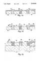
- FIG. 1is a top plan view of a peripheral to area adapter illustrating an embodiment with a rigid dielectric support
- FIG. 2is a cross-sectional view of the adapter in FIG. 1 further including an integrated circuit chip mounted on the adapter;
- FIG. 3is a cross-sectional view similar to FIG. 2 further including a heat transfer plate contacting the chip, a protective bumper surrounding the sides the adapter and chip to provide mechanical protection, and a substrate beneath the adapter;
- FIG. 4is a top plan view of a peripheral to area adapter illustrating an embodiment with a flexible TAB dielectric support
- FIG. 5is a cross-sectional view of the adapter in FIG. 4 further including an integrated circuit chip mounted on the adapter and a compressible supportive insulator between the adapter and the chip;
- FIG. 6is a cross-sectional view similar to FIG. 5 further including a heat transfer plate contacting the top of the chip, an encapsulant covering a portion of the adapter and chip to provide a seal for the chip, and a substrate beneath the adapter;
- FIG. 7is a top plan view of similar to FIG. 4 illustrating a plurality of TAB adapters on a reel of tape;
- FIGS. 8-14are cross-sectional views of a sequential manufacturing steps for the present invention adapter.
- FIG. 15is a cross-sectional view similar to FIG. 14 showing another embodiment of the present invention.
- Adapter 10comprises a rigid dielectric carrier support 12 with an upper surface 14 and lower surface 16. Suitable rigid dielectrics include silicon, photoceramic, ceramic, alumina, and glass ceramic. A large number of ceramic carriers 12 can be fabricated on a single wafer and then separated by sawing the wafer along scribe lines to form carriers with 600 mil sides. A plurality of electrical contact pads 18 are positioned near the peripheral edges of support 12. Pads 18 are 2 mils wide with a pad pitch of 4 mils (i.e. the pads are spaced by 2 mils with 4 mil center-to-center spacing).
- the present inventionis particularly well suited for high density structures in which at least two of the pads have a pitch of less than 10 mils.
- pads 18contain copper, nickel and gold and may be solder coated to facilitate subsequent bonding as will be described.
- a plurality of 2 mil wide planar copper conductive reroute lines 20are also on upper surface 14.
- Each reroute line 20comprises an first end 22 which terminates at a pad 18.
- Each reroute line 20also comprises second end 24.
- second ends 24fan-in from pads 18 toward the center of upper surface 14.
- the second ends 24 of reroute lines 20could, instead, fan-out away from pads 18 if desired. Fanning-in is preferred since this provides for a compact area array translation.
- each connected pad and reroute lineacts to customize or personalize the adapter 10 for a specific configuration of terminals on a chip.
- each reroute line 20is separated by a space 26 such as 20 mils from the other reroute lines to assure reroute lines 20 are electrically isolated from one another.
- Reroute line densities of up to 500 lines per inchare presently realizable by way of fabricating pads 18 and reroute lines 20 with thin film wiring techniques on a ceramic support 12, as will be later described.
- Integrated circuit chip 30comprises a plurality of conductive terminals 32 positioned along the outer periphery of chip bottom surface 34.
- terminals 32are bumps which protrude from surface 34.
- terminals 32can be in and aligned with surface 34.
- Chip 30further includes a plurality of internal circuits (not shown) integrated into a single semiconductor element and electrically coupled to terminals 32.
- Chip top surface 36is opposite chip bottom surface 34.
- Pads 18 on adapter 10are arranged in a pattern corresponding to terminals 32 so that when chip bottom surface 34 is positioned above support upper surface 14 the terminals 32 and pads 18 can be aligned, directly contacted and electrically coupled or bonded in a one-to-one relationship.
- Flip-chip attachment of a chip to a mating set of padsis well known in the art, see for instance U.S. Pat. No. 4,926,241 by Carey which is hereby incorporated by reference. Thermocompression is the preferred bonding technique. Solder reflow is also acceptable, as is adhesive bonding. Adhesive bonding would be preferred when terminals 32 are in and aligned with surface 34 of the chip.
- pads 18 and terminals 32could be welded together by directing a laser beam at the terminal/pad interface as described in U.S. Pat. No. 4,845,335 to Andrews et al. which is hereby incorporated by reference.
- Laser bondinghas the advantage of coupling laser energy to the bond without substantially heating the adapter or the chip, but is far more complex than other conventional bonding techniques.
- each second line end 24there is positioned beneath and electrically connected an electrically conductive vertical via 40 with a 10 mil diameter extending from support upper surface 14 to support lower surface 16. Openings for vias 40 can be formed by mechanically punching through-holes in a ceramic wafer before separating the individual supports 12. Vias 40 are formed by filling an electrically conductive metal into the holes. Alternatively, vias 40 can comprise a bore defined by a bore wall with an electrically conductive metal formed on the bore wall. In either case, the electrical conductor vias 40 are separated by the dielectric. The choice of conductive metals for vias 40 may depend on the nature of the ceramic. For standard high temperature fired ceramics, tungsten or other refractory metals are preferred.
- vias 40can be used as power or ground vias, and/or a capacitor (not shown) can be fabricated in support 12 with its electrodes connected to selected vias.
- each via 40there is electrically connected an electrical coupling element 42 on adapter lower surface 16, preferably protruding below lower surface 16.
- Each coupling element 42has at least a portion directly beneath an individual via 40.
- adapter 10provides peripheral to area translation for chip 30 by electrically interconnecting each peripheral chip terminal 32 to an electrical coupling element 42 beneath the adapter.
- Preferably coupling elements 42form a grid array pattern that fits within the area covered by chip 30. The array pattern also allows coupling elements 42 to have a substantially larger bonding area than terminals 32.
- the present invention adaptercan translate this terminal configuration into an array, within the area of the chip, containing 20 rows of coupling elements having sides 20 mils in width and length, and 20 mil spaces between adjacent coupling elements.
- the present invention adapterallows chips with widely varying terminal configurations to be conveniently connected to a generic substrate adapted to receive a standard area grid. That is, the present invention adapter 10 can utilize top surface metallization (pads 18 and planar reroute lines 20 ) customized for a particular chip 30, while also employing a support 12, vias 40, and coupling elements 42 fabricated to standard dimensions with standard materials.
- FIG. 3a cross-sectional view of the present invention similar to FIG. 2 is shown.
- An optional metallic heat transfer plate 50contacts the top surface 36 of chip 30 in heat exchange relationship to improve the removal of heat generated by chip 30.
- Plate 50can be 20 mils of copper-tungsten or kovar.
- a protective bumper 52such as rubber or silicone can be applied to the sides of the structure to provide a mechanical fender for the adapter 10 and chip 30, particularly if the sides or edges of chip 30 are mechanically fragile. As shown, protective bumper 52 is applied over heat plate sidewalls 54, chip sidewalls 56, terminal outer sidewalls 58, outer portion 60 of support 12 beyond terminal outer sidewalls 58, and support sidewalls 62. Protective bumper 52 should cover at least between top 36 of chip 30 and bottom surface 16 of adapter 12 to assure chip outer sidewalls 56 are mechanically shielded.
- An integrated circuit packaging structure of the present inventioncan further include an electrical interconnect substrate 70 such as the high-density high-performance customizable copper/polyimide structure disclosed in European Patent Application 88308996.3 by Carey.
- Substrate 70comprises a plurality of gold coated nickel bond sites 72 protruding from the substrate top surface 74 arranged in a pattern corresponding to coupling elements 42 so that each coupling element 42 can be aligned with and directly contact a separate bond site 72. That is, bond sites 72 are arranged in the same array pattern as coupling elements 42. Coupling elements 42 can then be bonded to bond sites 72 by numerous well known techniques. If solder reflow is used then tin plated copper bond sites 72 are preferred since gold tends to leach into solder.
- FIGS. 4-6there is seen another embodiment of the present invention wherein like parts to FIGS. 1-3 are similarly numbered with the addition of the suffix "a" and are identical unless otherwise specified.
- the support 12ais a thin (25 micron) flexible TAB tape 80.
- Pads 18aextend beyond outer sidewalls 62a.
- Reroute lines 20aare shown as fanning in, however, it may be desirable to further include a plurality of electrical test sites (not shown) at a second end of additional lines 20a which fan-out from pads 18a.
- coupling elements 42aare shown as wider that reroute lines 20a. Consequently, vias 40a are formed in a vertical pyramid-like shape.
- a compressible supportive insulator 96can be sandwiched between the flexible adapter 10a and chip 30a inside terminals 32a to provide mechanical support.
- Suitable insulators 96include silcone, rubber, or an elastomeric polymer foam.
- the surface area of supportive insulator 96is approximately the same as support 80 to allow supportive insulator outer sidewalls 98 to align with support outer sidewalls 62a.
- Supportive insulator 96must be thin enough to permit pads 18a to contact terminals 32a, yet must be thick enough to contact adapter upper surface 14a and chip bottom surface 34a in order to reduce the pressure and stress upon pads 18a and terminals 32a.
- outer sidewalls 54a of heat transfer plate 50acan be spaced a small distance from sidewalls 56a of chip 30a thereby leaving an end portion 100 of chip top surface 36a uncovered.
- an encapsulant 102such as 100 mils of molded plastic can he applied over heat plate sidewalls 54a, chip top surface portions 100, chip sidewalls 56a, the bottom of pads 18a, support sidewalls 62a, adapter lower surface 16a and lower portions 104 of coupling elements 42a. That is, encapsulant 102 covers the entire packaging structure except for an least a portion of heat transfer plate 50a, and at least upper portions 106 of coupling elements 42a which protrude from encapsulant 102.
- Encapsulant 102can also fill regions 108 between compressible supportive insulator 96 and terminals 32a. If no heat transfer plate is used then encapsulant 102 can cover the entire top surface 36a of chip 30a. In either case the 100 mil thickness of encapsulant 102 will not substantially increase the size of the chip/adapter package.
- the chip/adapter packagecan be mounted on pads 72a of interconnect substrate 70a as previously described.
- FIG. 7there is shown a top plan view of a plurality of adapters 10a fabricated on a tape-automated-bonding (TAB) tape frame 110.
- Tape 110is produced in reel-to-reel form and includes sprocket holes 112 adjacent tape outer edges 114 to provide for advancing and aligning the tape.
- FIGS. 8-14a method of manufacturing the present invention adapter 10a is now described.
- a 25 micron thick polyimide layerforms support 80 of tape 110
- holes 118are punched or etched through support 80 to create openings for vias 40a.
- a 500 angstrom adhesion layer of chrome 120is deposited over support 80 which is in turn covered by 2500 angstroms of copper 122.
- photoresist mask 124covers selected portions of adapter 10a outside holes 118
- FIG. 12a 0.5 mil copper (or substantially copper) layer 126 is electroplated over the exposed portions of layer 122 to form pads 18a, reroute lines 20a and vias 40a.
- FIG. 8a 25 micron thick polyimide layer forms support 80 of tape 110
- holes 118are punched or etched through support 80 to create openings for vias 40a.
- a 500 angstrom adhesion layer of chrome 120is deposited over support 80 which is in turn covered by 2500 angstroms of copper 122.
- adapter 10aserves as an upper thin film wiring layer for a thick, rigid support 12 by repeating steps in FIGS. 8-14 on an underlaying rigid support 12. That is, adapter 10a can be considered an upper dielectric layer 130 of support 12. Layer 130 includes upper pads 18a and reroute lines 20a on the top surface, and upper vias 40a therethrough. If desired, upper coupling elements 42a (not shown) may protrude from the bottom 16a of support 12a at vias 40a. The tops of vias 40 in rigid support 12 are preferably at least twice as wide as the bottoms of upper vias 40a in order to facilitate alignment and direct contact between vias 40 and 40a.
- the present invention adapterprovides for a plurality of chips to be densely packaged on a substrate and electrically interconnected to one another. However, it may be advantageous to test various electrical interconnections prior to testing the final packaging structure.
- a connection hierarchy of chip to adapter and adapter to substrateallows for incrementally testing the chip to adapter bonds (between pads 18 and terminals 32) before bonding the adapter to the substrate (coupling elements 42 to bond sites 72).
- the thermal coefficient of expansion (TCE) for the adapter and one or both of the integrated circuit and substratecan be substantially matched by the appropriate choice of materials; such as by using silicon in the integrated circuit and silicon (or glass or glass ceramics with TCEs similar to silicon) in the adapter and the substrate.
- the protective bumpercould be used with a rigid carrier support and the molded plastic seal could be used with a TAB carrier support.
Landscapes
- Physics & Mathematics (AREA)
- Condensed Matter Physics & Semiconductors (AREA)
- General Physics & Mathematics (AREA)
- Engineering & Computer Science (AREA)
- Computer Hardware Design (AREA)
- Microelectronics & Electronic Packaging (AREA)
- Power Engineering (AREA)
- Wire Bonding (AREA)
Abstract
Description
This is a continuation of U.S. Ser. No. 08/176,924 filed Jan. 3, 1994 now abandoned, which is a continuation of U.S. Ser. No. 08/017,580 filed Feb. 16, 1993, U.S. Pat. No. 5,289,346, which is a continuation of U.S. Ser. No. 07/887,198 filed May 21, 1992 now abandoned, which is a continuation of U.S. Ser. No. 07/661,579 filed Feb. 26, 1991 now abandoned. These applications are incorporated herein by reference.
1. Field of the Invention
The present invention relates to a carrier adapter use between an integrated circuit chip with peripheral terminals and an underlying substrate with area-patterned bond sites, and more particularly to an adapter with mating pads on the top surface of the adapter that can be aligned with, connected directly with and bonded to peripheral terminals on a chip, reroute lines on the top surface of the adapter with first ends connected to the pads, and vertical through-vias connected to the second ends of the reroute lines that terminate at coupling elements in an array pattern on the bottom of the adapter.
2. Description of the Related Art
Current multi-chip circuitry design requires attachment of numerous electronic devices to an electrical interconnect substrate. Terminals on the electrical devices can be connected to pads on the surface of the substrates. The substrate can further include buried metal lines which interconnect selected pads, thereby providing electrical interconnection for the electronic devices.
Typically the conductive terminals on a high density integrated circuit chip are distributed over a very small area along the periphery of the top surface of the chip Flip-chip bonding involves inverting the chip, aligning the terminals on the chip with pads on the substrate, contacting the terminals to the pads and then bonding the terminals to the pads.
There also exist adapters which can be sandwiched between an inverted integrated circuit and an underlying interconnect substrate. In particular, existing adapters can translate the conductive terminals on a chip to an array pattern of coupling elements, to be bonded to the substrate, which can be positioned inside the area of the chip and have substantially larger bonding faces than the terminals. The array pattern of coupling elements can also have generic configurations and dimensions suitable for a wide variety of substrates.
Kyocera has developed an adapter which uses the internal layers of a multilayer ceramic carrier to accomplish the translation, but must modify the ceramic fabrication process in order to customize the adapter for a terminal configuration. An adapter by Fujitsu connects the inner ends of bent leads to the terminals on the bottom of a chip, and the outer ends of the bent leads to the pads on an adapter, but requires two bonding steps for each terminal.
Accordingly, there exists a need for an improved adapter capable of providing peripheral to area translation for the terminals on an integrated circuit chip.
An object of the present invention is to provide an adapter for integrated circuit chips that contains pads on the top surface customized to directly contact the conductive peripheral terminals on a specific integrated circuit chip, planar reroute lines on the top surface that are customized to translate the terminals into a standardized array pattern, and vias through a dielectric support that connects the reroute lines to coupling elements on the bottom of the adapter. All of the peripheral to area translation for the terminals is performed by the reroute lines.
Another object of the present invention is to improve the assembly and testability of an integrated circuit-interconnect substrate structure without a substantial real estate penalty.
A further object of the present invention is to provide an improved technique for single chip mounting to multi chip modules and printed wiring boards.
Still a further object of the present invention is to translate a perimeter format on a chip into a compact area array no larger than the area of the chip.
A feature of the present invention is to provide a peripheral to area adapter of the type adapted to receive an integrated circuit, the integrated circuit including a top surface, a bottom surface, and a plurality of conductive terminals positioned along the periphery of the bottom surface, including a dielectric support having an upper surface and a lower surface; a plurality of electrically conductive pads above the upper surface of the support and arranged in a pattern corresponding to the terminals on the integrated circuit, so that the bottom surface of the integrated circuit can be positioned above the upper surface of the support to align, directly contact and bond the terminals to the pads; a plurality of electrically conductive planar reroute lines above the upper surface of the support, each of the reroute lines having a first end at a pad and a second end; a plurality of electrically conductive vertical vias extending from the upper surface of the support to the lower surface of the support, each of the vias positioned directly beneath and electrically connected to the second end of a reroute line; and a plurality of electrical coupling elements in an array pattern on the lower surface of the support, each of the coupling elements having at least a portion directly beneath and electrically connected to a via; wherein the adapter can provide peripheral to area translation for the terminals on the integrated circuit, and all of the peripheral to area translation is performed by the reroute lines.
Another feature of the present invention is wherein the vias are substantially filled with an electrically conductive metal, or alternatively the vias comprise a bore defined by a bore wall extending between the upper and lower surfaces of the support, and an electrically conductive metal formed on the bore wall.
An additional feature of the present invention is wherein the reroute lines fan-in from the pads.
Yet another feature of the present invention is wherein the dielectric support is a rigid ceramic carrier.
An additional feature of the present invention is wherein the pads and reroute lines are fabricated from thin film wiring.
Another feature of the present invention is wherein the pads and reroute lines are formed on a tape-automated-bonding frame.
Still another feature of the present invention is wherein the terminals on the integrated circuit are bumps which protrude from the bottom surface of the integrated circuit.
Yet another feature of the present invention is wherein the adapter is combined with an integrated circuit to form an integrated circuit package.
A further feature of the present invention is wherein a compressible supportive insulator is positioned inside the terminals between the bottom surface of the integrated circuit and the top of the adapter.
Still a further feature of the present invention is wherein an encapsulant surrounds at least the sides of the package between the top surface of the chip and the lower surface of the support, thereby providing a seal for the chip.
Another feature of the present invention is wherein a protective bumper is attached to the sides of the package between the top surface of the chip and the lower surface of the support, thereby providing a mechanical shield for the sides of the chip.
Still another feature of the present invention is wherein a metallic heat transfer plate contacts in heat exchange relationship at least a portion of the top surface of the chip.
A still further feature of the present invention is wherein the adapter is combined with an integrated circuit and an underlying electrical interconnect substrate to form an integrated circuit packaging structure.
An advantage of the present invention is that the adapter may allow for increasing the mechanical and thermal coefficient of expansion (TCE) comparability of a packaging structure by using a support material with substantially the same TCE as the integrated circuit and the substrate.
Other objects, features and advantages of the present invention will be apparent from a review of the detailed description of the preferred embodiments which follows, when taken together with the drawings, a brief description of which follows.
In the drawings:
FIG. 1 is a top plan view of a peripheral to area adapter illustrating an embodiment with a rigid dielectric support;
FIG. 2 is a cross-sectional view of the adapter in FIG. 1 further including an integrated circuit chip mounted on the adapter;
FIG. 3 is a cross-sectional view similar to FIG. 2 further including a heat transfer plate contacting the chip, a protective bumper surrounding the sides the adapter and chip to provide mechanical protection, and a substrate beneath the adapter;
FIG. 4 is a top plan view of a peripheral to area adapter illustrating an embodiment with a flexible TAB dielectric support;
FIG. 5 is a cross-sectional view of the adapter in FIG. 4 further including an integrated circuit chip mounted on the adapter and a compressible supportive insulator between the adapter and the chip;
FIG. 6 is a cross-sectional view similar to FIG. 5 further including a heat transfer plate contacting the top of the chip, an encapsulant covering a portion of the adapter and chip to provide a seal for the chip, and a substrate beneath the adapter;
FIG. 7 is a top plan view of similar to FIG. 4 illustrating a plurality of TAB adapters on a reel of tape;
FIGS. 8-14 are cross-sectional views of a sequential manufacturing steps for the present invention adapter; and
FIG. 15 is a cross-sectional view similar to FIG. 14 showing another embodiment of the present invention.
Referring now to the drawings, and particularly to FIG. 1, there is shown a top plan view of a peripheral to area adapter generally designated byreference numeral 10.Adapter 10 comprises a rigiddielectric carrier support 12 with anupper surface 14 andlower surface 16. Suitable rigid dielectrics include silicon, photoceramic, ceramic, alumina, and glass ceramic. A large number ofceramic carriers 12 can be fabricated on a single wafer and then separated by sawing the wafer along scribe lines to form carriers with 600 mil sides. A plurality ofelectrical contact pads 18 are positioned near the peripheral edges ofsupport 12.Pads 18 are 2 mils wide with a pad pitch of 4 mils (i.e. the pads are spaced by 2 mils with 4 mil center-to-center spacing). The present invention is particularly well suited for high density structures in which at least two of the pads have a pitch of less than 10 mils. Preferablypads 18 contain copper, nickel and gold and may be solder coated to facilitate subsequent bonding as will be described. A plurality of 2 mil wide planar copper conductive reroutelines 20 are also onupper surface 14. Each rerouteline 20 comprises anfirst end 22 which terminates at apad 18. Each rerouteline 20 also comprisessecond end 24. In the example set forth, second ends 24 fan-in frompads 18 toward the center ofupper surface 14. However, it is understood that the second ends 24 of reroutelines 20 could, instead, fan-out away frompads 18 if desired. Fanning-in is preferred since this provides for a compact area array translation. In any event, each connected pad and reroute line acts to customize or personalize theadapter 10 for a specific configuration of terminals on a chip. Returning to the example, each rerouteline 20 is separated by aspace 26 such as 20 mils from the other reroute lines to assure reroutelines 20 are electrically isolated from one another. Reroute line densities of up to 500 lines per inch are presently realizable by way of fabricatingpads 18 and reroutelines 20 with thin film wiring techniques on aceramic support 12, as will be later described.
With reference now to FIG. 2, there is shown a cross-sectional view ofadapter 10 as part of a chip/adapter package. Integratedcircuit chip 30 comprises a plurality ofconductive terminals 32 positioned along the outer periphery of chipbottom surface 34. In the preferred embodiment, as illustrated herein,terminals 32 are bumps which protrude fromsurface 34. Alternatively, however,terminals 32 can be in and aligned withsurface 34.Chip 30 further includes a plurality of internal circuits (not shown) integrated into a single semiconductor element and electrically coupled toterminals 32. Chiptop surface 36 is opposite chipbottom surface 34.Pads 18 onadapter 10 are arranged in a pattern corresponding toterminals 32 so that when chipbottom surface 34 is positioned above supportupper surface 14 theterminals 32 andpads 18 can be aligned, directly contacted and electrically coupled or bonded in a one-to-one relationship. Flip-chip attachment of a chip to a mating set of pads is well known in the art, see for instance U.S. Pat. No. 4,926,241 by Carey which is hereby incorporated by reference. Thermocompression is the preferred bonding technique. Solder reflow is also acceptable, as is adhesive bonding. Adhesive bonding would be preferred whenterminals 32 are in and aligned withsurface 34 of the chip. The use of an adhesive material for bonding electrical contacts together is known in the art, see, for instance, U.S. Ser. No. 07/631,296 filed Dec. 20, 1990 by MacKay; K. Sakuma et al., "Chip on Glass Technology With Standard Aluminized IC Chip", International Society For Hybrid Microelectronics Conference Proceedings, Chicago, Ill., Oct. 13, 1990, pp. 250-256; and P. Hogerton et al., "Investigations Into The Use Of Adhesives For Level-1 Microelectronic Interconnections", Materials Research Society. Symposium Proceeding, Vol. 154, San Diego, Calif., Apr. 24, 1989, pp. 415-424; the disclosures for which are hereby incorporated by reference Orpads 18 andterminals 32 could be welded together by directing a laser beam at the terminal/pad interface as described in U.S. Pat. No. 4,845,335 to Andrews et al. which is hereby incorporated by reference. Laser bonding has the advantage of coupling laser energy to the bond without substantially heating the adapter or the chip, but is far more complex than other conventional bonding techniques.
For eachsecond line end 24, there is positioned beneath and electrically connected an electrically conductive vertical via 40 with a 10 mil diameter extending from supportupper surface 14 to supportlower surface 16. Openings forvias 40 can be formed by mechanically punching through-holes in a ceramic wafer before separating the individual supports 12.Vias 40 are formed by filling an electrically conductive metal into the holes. Alternatively, vias 40 can comprise a bore defined by a bore wall with an electrically conductive metal formed on the bore wall. In either case, the electrical conductor vias 40 are separated by the dielectric. The choice of conductive metals forvias 40 may depend on the nature of the ceramic. For standard high temperature fired ceramics, tungsten or other refractory metals are preferred. But for lower temperature firing ceramics such as glass ceramic, copper or gold are preferred. If desired, a subset ofvias 40 can be used as power or ground vias, and/or a capacitor (not shown) can be fabricated insupport 12 with its electrodes connected to selected vias.
For each via 40, there is electrically connected anelectrical coupling element 42 on adapterlower surface 16, preferably protruding belowlower surface 16. Eachcoupling element 42 has at least a portion directly beneath an individual via 40. Thusadapter 10 provides peripheral to area translation forchip 30 by electrically interconnecting eachperipheral chip terminal 32 to anelectrical coupling element 42 beneath the adapter. Preferably couplingelements 42 form a grid array pattern that fits within the area covered bychip 30. The array pattern also allowscoupling elements 42 to have a substantially larger bonding area thanterminals 32.
For instance, suppose a chip has a square top surface with 400 mil sides and 400 I/O terminals. An efficient terminal configuration might position 100 terminals per side, with each terminal 2 mils in width and spaced 2 mils from adjacent terminals. The present invention adapter can translate this terminal configuration into an array, within the area of the chip, containing 20 rows of couplingelements having sides 20 mils in width and length, and 20 mil spaces between adjacent coupling elements. In addition, the present invention adapter allows chips with widely varying terminal configurations to be conveniently connected to a generic substrate adapted to receive a standard area grid. That is, thepresent invention adapter 10 can utilize top surface metallization (pads 18 and planar reroute lines 20 ) customized for aparticular chip 30, while also employing asupport 12, vias 40, andcoupling elements 42 fabricated to standard dimensions with standard materials.
Referring now to FIG. 3, a cross-sectional view of the present invention similar to FIG. 2 is shown. An optional metallicheat transfer plate 50 contacts thetop surface 36 ofchip 30 in heat exchange relationship to improve the removal of heat generated bychip 30.Plate 50 can be 20 mils of copper-tungsten or kovar.
If desired, aprotective bumper 52 such as rubber or silicone can be applied to the sides of the structure to provide a mechanical fender for theadapter 10 andchip 30, particularly if the sides or edges ofchip 30 are mechanically fragile. As shown,protective bumper 52 is applied over heat plate sidewalls 54, chip sidewalls 56, terminalouter sidewalls 58, outer portion 60 ofsupport 12 beyond terminalouter sidewalls 58, and support sidewalls 62.Protective bumper 52 should cover at least between top 36 ofchip 30 andbottom surface 16 ofadapter 12 to assure chipouter sidewalls 56 are mechanically shielded.
An integrated circuit packaging structure of the present invention can further include anelectrical interconnect substrate 70 such as the high-density high-performance customizable copper/polyimide structure disclosed in European Patent Application 88308996.3 by Carey.Substrate 70 comprises a plurality of gold coatednickel bond sites 72 protruding from thesubstrate top surface 74 arranged in a pattern corresponding tocoupling elements 42 so that eachcoupling element 42 can be aligned with and directly contact aseparate bond site 72. That is,bond sites 72 are arranged in the same array pattern ascoupling elements 42. Couplingelements 42 can then be bonded tobond sites 72 by numerous well known techniques. If solder reflow is used then tin platedcopper bond sites 72 are preferred since gold tends to leach into solder.
With reference now to FIGS. 4-6, there is seen another embodiment of the present invention wherein like parts to FIGS. 1-3 are similarly numbered with the addition of the suffix "a" and are identical unless otherwise specified.
Referring now to FIG. 4, in this embodiment thesupport 12a is a thin (25 micron)flexible TAB tape 80.Pads 18a extend beyondouter sidewalls 62a. Reroutelines 20a are shown as fanning in, however, it may be desirable to further include a plurality of electrical test sites (not shown) at a second end ofadditional lines 20a which fan-out frompads 18a.
With reference now to FIG. 5,coupling elements 42a are shown as wider that reroutelines 20a. Consequently,vias 40a are formed in a vertical pyramid-like shape. In addition, a compressiblesupportive insulator 96 can be sandwiched between theflexible adapter 10a andchip 30a insideterminals 32a to provide mechanical support.Suitable insulators 96 include silcone, rubber, or an elastomeric polymer foam. The surface area ofsupportive insulator 96 is approximately the same assupport 80 to allow supportive insulatorouter sidewalls 98 to align with supportouter sidewalls 62a.Supportive insulator 96 must be thin enough to permitpads 18a to contactterminals 32a, yet must be thick enough to contact adapter upper surface 14a and chip bottom surface 34a in order to reduce the pressure and stress uponpads 18a andterminals 32a.
Referring now to FIG. 6, if a seal is desired,outer sidewalls 54a ofheat transfer plate 50a can be spaced a small distance fromsidewalls 56a ofchip 30a thereby leaving anend portion 100 of chiptop surface 36a uncovered. Then an encapsulant 102 such as 100 mils of molded plastic can he applied overheat plate sidewalls 54a, chiptop surface portions 100,chip sidewalls 56a, the bottom ofpads 18a,support sidewalls 62a, adapterlower surface 16a andlower portions 104 ofcoupling elements 42a. That is,encapsulant 102 covers the entire packaging structure except for an least a portion ofheat transfer plate 50a, and at leastupper portions 106 ofcoupling elements 42a which protrude fromencapsulant 102.Encapsulant 102 can also fillregions 108 between compressiblesupportive insulator 96 andterminals 32a. If no heat transfer plate is used then encapsulant 102 can cover the entiretop surface 36a ofchip 30a. In either case the 100 mil thickness ofencapsulant 102 will not substantially increase the size of the chip/adapter package. The chip/adapter package can be mounted onpads 72a ofinterconnect substrate 70a as previously described.
Referring now to FIG. 7, there is shown a top plan view of a plurality ofadapters 10a fabricated on a tape-automated-bonding (TAB)tape frame 110.Tape 110 is produced in reel-to-reel form and includes sprocket holes 112 adjacent tapeouter edges 114 to provide for advancing and aligning the tape.
Referring now to FIGS. 8-14, a method of manufacturing thepresent invention adapter 10a is now described. In FIG. 8 a 25 micron thick polyimide layer forms support 80 oftape 110 In FIG. 9holes 118 are punched or etched throughsupport 80 to create openings forvias 40a. In FIG. 10 a 500 angstrom adhesion layer ofchrome 120 is deposited oversupport 80 which is in turn covered by 2500 angstroms ofcopper 122. In FIG. 11photoresist mask 124 covers selected portions ofadapter 10a outsideholes 118, and in FIG. 12 a 0.5 mil copper (or substantially copper)layer 126 is electroplated over the exposed portions oflayer 122 to formpads 18a, reroutelines 20a andvias 40a. In FIG. 13mask 124 is stripped. In FIG. 14 the entire surface is "flash-etched" to remove the uncovered regions oflayers pads 18a and reroutelines 20a, but such top portion will be negligible sincelayer 126 is much thicker thanlayers adapters 10a are formed they can be excised fromtape 110 prior to bonding to achip 30a.
Referring now to FIG. 15, another embodiment for the method of manufacturing the present invention in FIGS. 8-14 is now described. In this embodiment,adapter 10a serves as an upper thin film wiring layer for a thick,rigid support 12 by repeating steps in FIGS. 8-14 on an underlayingrigid support 12. That is,adapter 10a can be considered anupper dielectric layer 130 ofsupport 12.Layer 130 includesupper pads 18a and reroutelines 20a on the top surface, andupper vias 40a therethrough. If desired,upper coupling elements 42a (not shown) may protrude from the bottom 16a ofsupport 12a atvias 40a. The tops ofvias 40 inrigid support 12 are preferably at least twice as wide as the bottoms ofupper vias 40a in order to facilitate alignment and direct contact betweenvias
The present invention adapter provides for a plurality of chips to be densely packaged on a substrate and electrically interconnected to one another. However, it may be advantageous to test various electrical interconnections prior to testing the final packaging structure. A connection hierarchy of chip to adapter and adapter to substrate allows for incrementally testing the chip to adapter bonds (betweenpads 18 and terminals 32) before bonding the adapter to the substrate (coupling elements 42 to bond sites 72).
The thermal coefficient of expansion (TCE) for the adapter and one or both of the integrated circuit and substrate can be substantially matched by the appropriate choice of materials; such as by using silicon in the integrated circuit and silicon (or glass or glass ceramics with TCEs similar to silicon) in the adapter and the substrate.
Numerous variations of the previously described embodiments are apparent to those with skill in the art. For instance, the protective bumper could be used with a rigid carrier support and the molded plastic seal could be used with a TAB carrier support.
The present invention, therefore, is well adapted to carry out the objects and attain the ends and advantages mentioned, as well as others inherent therein. While presently preferred embodiments of the invention have been described for the purpose of disclosure, numerous changes in the details of construction and arrangement of parts may be made without departing from the spirit of the present invention and the scope of the appended claims.
Claims (8)
1. A compact adapter package providing peripheral to area translation for an integrated circuit chip, comprising:
a single integrated circuit chip having top and bottom surfaces and having a plurality of conductive terminals disposed on the bottom surface wherein the entire bottom surface of the chip forms a major surface area of the chip and a portion of the major surface area inside the terminals towards the center of the chip forms an inner surface area of the chip;
a dielectric support having upper and lower surfaces wherein the support is positioned entirely within the inner surface area of the chip and the bottom surface of the chip is spaced from and faces the upper surface of the support;
a plurality of electrically conductive pads extending laterally from the upper surface of the support wherein the pads are aligned with and bonded in one-to-one relationship to the terminals thereby attaching the chip to the support wherein the pads, terminals and bonds are positioned entirely within the major surface area of the chip outside the inner surface area of the chip;
a plurality of flat electrically conductive horizontal reroute lines on the upper surface of the support wherein each reroute line includes a first end at one of said pads and a second end within the inner surface area of the chip wherein the reroute lines are positioned entirely within the major surface area of the chip and disposed entirely above and parallel to the upper surface of the support;
a plurality of electrically conductive vertical vias extending through the support between the upper and lower surfaces of the support wherein each via is positioned entirely within the inner surface area of the chip and positioned directly beneath and electrically connected to the second end of one of said reroute lines; and
a plurality of coupling elements in an array pattern on the bottom surface of the support wherein each coupling element is positioned entirely within the inner surface area of the chip and includes a portion directly beneath and electrically connected to one of said vias such that each terminal is electrically connected to one of said coupling elements;
wherein each terminal is electrically connected to a single pad, reroute line, via and coupling element, the reroute lines provide all horizontal translation between the terminals and the coupling elements, and the vias provide all vertical translation between the terminals and the coupling elements.
2. The adapter package of claim 1 wherein the bonds between the terminals and the pads constitute the sole means for attaching the chip to the support.
3. The adapter package of claim 1 wherein the support is a flexible tape-automated-bonding frame.
4. A compact adapter package providing peripheral to area translation for an integrated circuit chip, comprising:
a single integrated circuit chip having top and bottom surfaces and having a plurality of conductive terminals disposed on the bottom surface wherein the entire bottom surface of the chip forms a major surface area of the chip and a portion of the major surface area inside the terminals towards the center of the chip forms an inner surface area of the chip;
a dielectric support having upper and lower surfaces wherein the support is positioned entirely within the inner surface area of the chip and the bottom surface of the chip is spaced from and faces the upper surface of the support;
a compressible supportive insulator between the bottom surface of the chip and the upper surface of the support wherein the compressible supportive insulator is positioned entirely within the inner surface area of the chip and outer sidewalls of the compressible supportive insulator are aligned with outer sidewalls of the support;
a plurality of electrically conductive pads extending laterally from the upper surface of the support wherein the pads are aligned with and bonded in one-to-one relationship to the terminals thereby attaching the chip to the support wherein the pads, terminals and bonds are positioned entirely within the major surface area of the chip outside the inner surface area of the chip;
a plurality of flat electrically conductive horizontal reroute lines on the upper surface of the support wherein each reroute line includes a first end at one of said pads and a second end within the inner surface area of the chip wherein the reroute lines are positioned entirely within the major surface area of the chip and disposed entirely above and parallel to the upper surface of the support;
a plurality of electrically conductive vertical vias extending through the support between the upper and lower surfaces of the support wherein each via is positioned entirely within the inner surface area of the chip and positioned directly beneath and electrically connected to the second end of one of said reroute lines; and
a plurality of coupling elements in an array pattern on the bottom surface the support wherein each coupling element is positioned entirely within the inner surface area of the chip and includes a portion directly beneath and electrically connected to one of said vias such that each terminal is electrically connected to one of said coupling elements;
wherein each terminal is electrically connected to a single pad, reroute line, via and coupling element, the reroute lines provide all horizontal translation between the terminals and the coupling elements, and the vias provide all vertical translation between the terminals and the coupling elements.
5. The adapter package of claim 4 wherein the compressible supportive insulator contacts the bottom surface of the chip, the upper surface of the support and the reroute lines.
6. The adapter package of claim 4 wherein the compressible supportive insulator is selected from the group consisting of silicone, rubber and elastomeric polymer foam.
7. The adapter package of claim 4 wherein the bonds between the terminals and the pads constitute the sole means for attaching the chip to the support.
8. The adapter package of claim 4 wherein the support is a flexible tape-automated-bonding frame.
Priority Applications (1)
| Application Number | Priority Date | Filing Date | Title |
|---|---|---|---|
| US08/257,235US5379191A (en) | 1991-02-26 | 1994-06-09 | Compact adapter package providing peripheral to area translation for an integrated circuit chip |
Applications Claiming Priority (5)
| Application Number | Priority Date | Filing Date | Title |
|---|---|---|---|
| US66157991A | 1991-02-26 | 1991-02-26 | |
| US88719892A | 1992-05-21 | 1992-05-21 | |
| US08/017,580US5289346A (en) | 1991-02-26 | 1993-02-16 | Peripheral to area adapter with protective bumper for an integrated circuit chip |
| US17692494A | 1994-01-03 | 1994-01-03 | |
| US08/257,235US5379191A (en) | 1991-02-26 | 1994-06-09 | Compact adapter package providing peripheral to area translation for an integrated circuit chip |
Related Parent Applications (1)
| Application Number | Title | Priority Date | Filing Date |
|---|---|---|---|
| US17692494AContinuation | 1991-02-26 | 1994-01-03 |
Publications (1)
| Publication Number | Publication Date |
|---|---|
| US5379191Atrue US5379191A (en) | 1995-01-03 |
Family
ID=27486668
Family Applications (1)
| Application Number | Title | Priority Date | Filing Date |
|---|---|---|---|
| US08/257,235Expired - LifetimeUS5379191A (en) | 1991-02-26 | 1994-06-09 | Compact adapter package providing peripheral to area translation for an integrated circuit chip |
Country Status (1)
| Country | Link |
|---|---|
| US (1) | US5379191A (en) |
Cited By (81)
| Publication number | Priority date | Publication date | Assignee | Title |
|---|---|---|---|---|
| US5625944A (en)* | 1992-12-30 | 1997-05-06 | Interconnect Systems, Inc. | Methods for interconnecting integrated circuits |
| US5679977A (en)* | 1990-09-24 | 1997-10-21 | Tessera, Inc. | Semiconductor chip assemblies, methods of making same and components for same |
| US5682061A (en)* | 1990-09-24 | 1997-10-28 | Tessera, Inc. | Component for connecting a semiconductor chip to a substrate |
| US5686676A (en)* | 1996-05-07 | 1997-11-11 | Brush Wellman Inc. | Process for making improved copper/tungsten composites |
| US5784262A (en)* | 1995-11-06 | 1998-07-21 | Symbios, Inc. | Arrangement of pads and through-holes for semiconductor packages |
| US5820014A (en) | 1993-11-16 | 1998-10-13 | Form Factor, Inc. | Solder preforms |
| US5891753A (en)* | 1997-01-24 | 1999-04-06 | Micron Technology, Inc. | Method and apparatus for packaging flip chip bare die on printed circuit boards |
| US5929517A (en)* | 1994-12-29 | 1999-07-27 | Tessera, Inc. | Compliant integrated circuit package and method of fabricating the same |
| US5994152A (en) | 1996-02-21 | 1999-11-30 | Formfactor, Inc. | Fabricating interconnects and tips using sacrificial substrates |
| US6048753A (en)* | 1996-04-02 | 2000-04-11 | Micron Technology, Inc. | Standardized bonding location process and apparatus |
| US6097099A (en)* | 1995-10-20 | 2000-08-01 | Texas Instruments Incorporated | Electro-thermal nested die-attach design |
| US6098283A (en)* | 1996-12-19 | 2000-08-08 | Intel Corporation | Method for filling vias in organic, multi-layer packages |
| US6117797A (en)* | 1998-09-03 | 2000-09-12 | Micron Technology, Inc. | Attachment method for heat sinks and devices involving removal of misplaced encapsulant |
| US6130480A (en)* | 1997-08-20 | 2000-10-10 | Oki Electric Industry Co., Ltd. | Structure for packaging semiconductor chip |
| US6133627A (en) | 1990-09-24 | 2000-10-17 | Tessera, Inc. | Semiconductor chip package with center contacts |
| US6194668B1 (en)* | 1997-12-22 | 2001-02-27 | Shinko Electric Industries Co., Ltd. | Multi-layer circuit board |
| US6246121B1 (en)* | 1999-04-12 | 2001-06-12 | Vlsi Technology, Inc. | High performance flip-chip semiconductor device |
| US6274823B1 (en) | 1993-11-16 | 2001-08-14 | Formfactor, Inc. | Interconnection substrates with resilient contact structures on both sides |
| US20010030370A1 (en)* | 1990-09-24 | 2001-10-18 | Khandros Igor Y. | Microelectronic assembly having encapsulated wire bonding leads |
| US20020155728A1 (en)* | 1990-09-24 | 2002-10-24 | Tessera, Inc. | Semiconductor chip assemblies, methods of making same and components for same |
| KR100352112B1 (en)* | 1996-12-06 | 2003-01-08 | 앰코 테크놀로지 코리아 주식회사 | Structure of chip-sized semiconductor package and fabricating method thereof |
| US20030107118A1 (en)* | 2001-10-09 | 2003-06-12 | Tessera, Inc. | Stacked packages |
| US20040032013A1 (en)* | 2002-08-15 | 2004-02-19 | Cobbley Chad A. | Semiconductor dice packages employing at least one redistribution layer and methods of fabrication |
| US20040031972A1 (en)* | 2001-10-09 | 2004-02-19 | Tessera, Inc. | Stacked packages |
| US20040105244A1 (en)* | 2002-08-06 | 2004-06-03 | Ilyas Mohammed | Lead assemblies with offset portions and microelectronic assemblies with leads having offset portions |
| US20050041398A1 (en)* | 2002-05-01 | 2005-02-24 | Huemoeller Ronald Patrick | Integrated circuit substrate having embedded back-side access conductors and vias |
| US20050173796A1 (en)* | 2001-10-09 | 2005-08-11 | Tessera, Inc. | Microelectronic assembly having array including passive elements and interconnects |
| US20060043569A1 (en)* | 2004-08-27 | 2006-03-02 | Benson Peter A | Low temperature methods of forming back side redistribution layers in association with through wafer interconnects, semiconductor devices including same, and assemblies |
| US20060215382A1 (en)* | 2000-10-20 | 2006-09-28 | Silverbrook Research Pty Ltd | Integrated circuit carrier |
| US20060237856A1 (en)* | 1993-11-16 | 2006-10-26 | Formfactor, Inc. | Microelectronic Contact Structure And Method Of Making Same |
| US7145238B1 (en) | 2004-05-05 | 2006-12-05 | Amkor Technology, Inc. | Semiconductor package and substrate having multi-level vias |
| US7185426B1 (en) | 2002-05-01 | 2007-03-06 | Amkor Technology, Inc. | Method of manufacturing a semiconductor package |
| US20080043447A1 (en)* | 2002-05-01 | 2008-02-21 | Amkor Technology, Inc. | Semiconductor package having laser-embedded terminals |
| US7334326B1 (en) | 2001-06-19 | 2008-02-26 | Amkor Technology, Inc. | Method for making an integrated circuit substrate having embedded passive components |
| US7501338B1 (en) | 2001-06-19 | 2009-03-10 | Amkor Technology, Inc. | Semiconductor package substrate fabrication method |
| US7548430B1 (en) | 2002-05-01 | 2009-06-16 | Amkor Technology, Inc. | Buildup dielectric and metallization process and semiconductor package |
| US7550857B1 (en) | 2006-11-16 | 2009-06-23 | Amkor Technology, Inc. | Stacked redistribution layer (RDL) die assembly package |
| US7589398B1 (en) | 2006-10-04 | 2009-09-15 | Amkor Technology, Inc. | Embedded metal features structure |
| US7633765B1 (en) | 2004-03-23 | 2009-12-15 | Amkor Technology, Inc. | Semiconductor package including a top-surface metal layer for implementing circuit features |
| US7670962B2 (en) | 2002-05-01 | 2010-03-02 | Amkor Technology, Inc. | Substrate having stiffener fabrication method |
| US20100078810A1 (en)* | 2008-09-30 | 2010-04-01 | Fujitsu Limited | Semiconductor apparatus, substrate design method, and substrate design apparatus |
| US20100093229A1 (en)* | 1996-02-21 | 2010-04-15 | Formfactor, Inc. | Microelectronic contact structure and method of making same |
| US7750250B1 (en) | 2006-12-22 | 2010-07-06 | Amkor Technology, Inc. | Blind via capture pad structure |
| US7752752B1 (en) | 2007-01-09 | 2010-07-13 | Amkor Technology, Inc. | Method of fabricating an embedded circuit pattern |
| US20110001232A1 (en)* | 2005-09-14 | 2011-01-06 | Htc Beteiligungs Gmbh | Flip-Chip Module and Method for the Production Thereof |
| US7960827B1 (en) | 2009-04-09 | 2011-06-14 | Amkor Technology, Inc. | Thermal via heat spreader package and method |
| US8222538B1 (en) | 2009-06-12 | 2012-07-17 | Amkor Technology, Inc. | Stackable via package and method |
| US8294276B1 (en) | 2010-05-27 | 2012-10-23 | Amkor Technology, Inc. | Semiconductor device and fabricating method thereof |
| US8300423B1 (en) | 2010-05-25 | 2012-10-30 | Amkor Technology, Inc. | Stackable treated via package and method |
| US8323771B1 (en) | 2007-08-15 | 2012-12-04 | Amkor Technology, Inc. | Straight conductor blind via capture pad structure and fabrication method |
| US8338229B1 (en) | 2010-07-30 | 2012-12-25 | Amkor Technology, Inc. | Stackable plasma cleaned via package and method |
| US8337657B1 (en) | 2010-10-27 | 2012-12-25 | Amkor Technology, Inc. | Mechanical tape separation package and method |
| US8471154B1 (en) | 2009-08-06 | 2013-06-25 | Amkor Technology, Inc. | Stackable variable height via package and method |
| US8482134B1 (en) | 2010-11-01 | 2013-07-09 | Amkor Technology, Inc. | Stackable package and method |
| US8525318B1 (en) | 2010-11-10 | 2013-09-03 | Amkor Technology, Inc. | Semiconductor device and fabricating method thereof |
| US8535961B1 (en) | 2010-12-09 | 2013-09-17 | Amkor Technology, Inc. | Light emitting diode (LED) package and method |
| US8536462B1 (en) | 2010-01-22 | 2013-09-17 | Amkor Technology, Inc. | Flex circuit package and method |
| US8557629B1 (en) | 2010-12-03 | 2013-10-15 | Amkor Technology, Inc. | Semiconductor device having overlapped via apertures |
| US8623753B1 (en) | 2009-05-28 | 2014-01-07 | Amkor Technology, Inc. | Stackable protruding via package and method |
| US8633598B1 (en) | 2011-09-20 | 2014-01-21 | Amkor Technology, Inc. | Underfill contacting stacking balls package fabrication method and structure |
| US8653674B1 (en) | 2011-09-15 | 2014-02-18 | Amkor Technology, Inc. | Electronic component package fabrication method and structure |
| US8717775B1 (en) | 2010-08-02 | 2014-05-06 | Amkor Technology, Inc. | Fingerprint sensor package and method |
| US8796561B1 (en) | 2009-10-05 | 2014-08-05 | Amkor Technology, Inc. | Fan out build up substrate stackable package and method |
| US8826531B1 (en) | 2005-04-05 | 2014-09-09 | Amkor Technology, Inc. | Method for making an integrated circuit substrate having laminated laser-embedded circuit layers |
| US8872329B1 (en) | 2009-01-09 | 2014-10-28 | Amkor Technology, Inc. | Extended landing pad substrate package structure and method |
| US8890329B2 (en) | 2011-04-26 | 2014-11-18 | Amkor Technology, Inc. | Semiconductor device |
| US8937381B1 (en) | 2009-12-03 | 2015-01-20 | Amkor Technology, Inc. | Thin stackable package and method |
| US9013011B1 (en) | 2011-03-11 | 2015-04-21 | Amkor Technology, Inc. | Stacked and staggered die MEMS package and method |
| US9029962B1 (en) | 2011-10-12 | 2015-05-12 | Amkor Technology, Inc. | Molded cavity substrate MEMS package fabrication method and structure |
| US9391043B2 (en) | 2012-11-20 | 2016-07-12 | Amkor Technology, Inc. | Semiconductor device and manufacturing method thereof |
| US9543242B1 (en) | 2013-01-29 | 2017-01-10 | Amkor Technology, Inc. | Semiconductor package and fabricating method thereof |
| US20170133625A1 (en)* | 2015-06-08 | 2017-05-11 | Boe Technology Group Co., Ltd. | Packaging Assembly and Packaging Method Thereof, and OLED Apparatus |
| US9691635B1 (en) | 2002-05-01 | 2017-06-27 | Amkor Technology, Inc. | Buildup dielectric layer having metallization pattern semiconductor package fabrication method |
| US9691734B1 (en) | 2009-12-07 | 2017-06-27 | Amkor Technology, Inc. | Method of forming a plurality of electronic component packages |
| US9704842B2 (en) | 2013-11-04 | 2017-07-11 | Amkor Technology, Inc. | Interposer, manufacturing method thereof, semiconductor package using the same, and method for fabricating the semiconductor package |
| US9704747B2 (en) | 2013-03-29 | 2017-07-11 | Amkor Technology, Inc. | Semiconductor device and manufacturing method thereof |
| US9721872B1 (en) | 2011-02-18 | 2017-08-01 | Amkor Technology, Inc. | Methods and structures for increasing the allowable die size in TMV packages |
| US9748154B1 (en) | 2010-11-04 | 2017-08-29 | Amkor Technology, Inc. | Wafer level fan out semiconductor device and manufacturing method thereof |
| US9960328B2 (en) | 2016-09-06 | 2018-05-01 | Amkor Technology, Inc. | Semiconductor device and manufacturing method thereof |
| US10811277B2 (en) | 2004-03-23 | 2020-10-20 | Amkor Technology, Inc. | Encapsulated semiconductor package |
| US11081370B2 (en) | 2004-03-23 | 2021-08-03 | Amkor Technology Singapore Holding Pte. Ltd. | Methods of manufacturing an encapsulated semiconductor device |
Citations (44)
| Publication number | Priority date | Publication date | Assignee | Title |
|---|---|---|---|---|
| US3541222A (en)* | 1969-01-13 | 1970-11-17 | Bunker Ramo | Connector screen for interconnecting adjacent surfaces of laminar circuits and method of making |
| UST955008I4 (en)* | 1974-08-19 | 1977-02-01 | International Business Machines Corporation | Flip chip structure including a silicon semiconductor element bonded to an Si3 N4 base substrate |
| US4074342A (en)* | 1974-12-20 | 1978-02-14 | International Business Machines Corporation | Electrical package for lsi devices and assembly process therefor |
| US4195195A (en)* | 1978-09-28 | 1980-03-25 | The United States Of America As Represented By The Secretary Of The Army | Tape automated bonding test board |
| US4249302A (en)* | 1978-12-28 | 1981-02-10 | Ncr Corporation | Multilayer printed circuit board |
| EP0052738A1 (en)* | 1980-11-25 | 1982-06-02 | Contraves Ag | Circuit board |
| US4349862A (en)* | 1980-08-11 | 1982-09-14 | International Business Machines Corporation | Capacitive chip carrier and multilayer ceramic capacitors |
| US4354107A (en)* | 1977-11-28 | 1982-10-12 | Irvine Sensors Corporation | Detector array module-structure and fabrication |
| US4403238A (en)* | 1980-12-08 | 1983-09-06 | Irvine Sensors Corporation | Detector array focal plane configuration |
| US4498122A (en)* | 1982-12-29 | 1985-02-05 | At&T Bell Laboratories | High-speed, high pin-out LSI chip package |
| US4525921A (en)* | 1981-07-13 | 1985-07-02 | Irvine Sensors Corporation | High-density electronic processing package-structure and fabrication |
| JPS60217641A (en)* | 1984-04-12 | 1985-10-31 | Nec Corp | Integrated circuit device |
| US4551629A (en)* | 1980-09-16 | 1985-11-05 | Irvine Sensors Corporation | Detector array module-structure and fabrication |
| US4617160A (en)* | 1984-11-23 | 1986-10-14 | Irvine Sensors Corporation | Method for fabricating modules comprising uniformly stacked, aligned circuit-carrying layers |
| US4631820A (en)* | 1984-08-23 | 1986-12-30 | Canon Kabushiki Kaisha | Mounting assembly and mounting method for an electronic component |
| FR2586885A1 (en)* | 1985-08-31 | 1987-03-06 | Nec Corp | Multi-layer wiring substrate |
| US4649990A (en)* | 1985-05-06 | 1987-03-17 | Hitachi, Ltd. | Heat-conducting cooling module |
| US4700473A (en)* | 1986-01-03 | 1987-10-20 | Motorola Inc. | Method of making an ultra high density pad array chip carrier |
| US4706166A (en)* | 1986-04-25 | 1987-11-10 | Irvine Sensors Corporation | High-density electronic modules--process and product |
| US4724472A (en)* | 1983-02-17 | 1988-02-09 | Fujitsu Limited | Semiconductor device |
| US4749120A (en)* | 1986-12-18 | 1988-06-07 | Matsushita Electric Industrial Co., Ltd. | Method of connecting a semiconductor device to a wiring board |
| JPS63172450A (en)* | 1987-01-12 | 1988-07-16 | Nec Corp | Wiring module |
| US4764846A (en)* | 1987-01-05 | 1988-08-16 | Irvine Sensors Corporation | High density electronic package comprising stacked sub-modules |
| JPS63308996A (en)* | 1987-06-11 | 1988-12-16 | Fujitsu Ltd | Method for measuring film thickness of resist for printed circuit boards |
| EP0310357A2 (en)* | 1987-09-29 | 1989-04-05 | Microelectronics and Computer Technology Corporation | Customizable circuitry |
| US4820013A (en)* | 1987-01-06 | 1989-04-11 | Alps Electric Co., Ltd. | LED array head |
| US4821142A (en)* | 1986-06-06 | 1989-04-11 | Hitachi, Ltd. | Ceramic multilayer circuit board and semiconductor module |
| US4845335A (en)* | 1988-01-28 | 1989-07-04 | Microelectronics And Computer Technology Corporation | Laser Bonding apparatus and method |
| US4851862A (en)* | 1988-08-05 | 1989-07-25 | Eastman Kodak Company | Led array printhead with tab bonded wiring |
| US4860088A (en)* | 1986-10-11 | 1989-08-22 | Microelectronics And Computer Technology Corporation | Electrical interconnect tape |
| US4866841A (en)* | 1987-09-16 | 1989-09-19 | Advanced Semiconductor Packages Ltd. | Integrated circuit chip carrier |
| JPH01293528A (en)* | 1988-05-23 | 1989-11-27 | Hitachi Ltd | Semiconductor device |
| US4912545A (en)* | 1987-09-16 | 1990-03-27 | Irvine Sensors Corporation | Bonding of aligned conductive bumps on adjacent surfaces |
| US4922377A (en)* | 1987-11-16 | 1990-05-01 | Hitachi, Ltd. | Module and a substrate for the module |
| US4926241A (en)* | 1988-02-19 | 1990-05-15 | Microelectronics And Computer Technology Corporation | Flip substrate for chip mount |
| US4926549A (en)* | 1988-05-31 | 1990-05-22 | Canon Kabushiki Kaisha | Method of producing electrical connection members |
| US4954878A (en)* | 1989-06-29 | 1990-09-04 | Digital Equipment Corp. | Method of packaging and powering integrated circuit chips and the chip assembly formed thereby |
| US4975765A (en)* | 1988-07-22 | 1990-12-04 | Contraves Ag | Highly integrated circuit and method for the production thereof |
| US4993954A (en)* | 1988-07-13 | 1991-02-19 | Thomson-Csf | Device for interconnection between and integrated circuit and an electrical circuit |
| US5006673A (en)* | 1989-12-07 | 1991-04-09 | Motorola, Inc. | Fabrication of pad array carriers from a universal interconnect structure |
| US5014161A (en)* | 1985-07-22 | 1991-05-07 | Digital Equipment Corporation | System for detachably mounting semiconductors on conductor substrate |
| US5029325A (en)* | 1990-08-31 | 1991-07-02 | Motorola, Inc. | TAB tape translator for use with semiconductor devices |
| US5061989A (en)* | 1990-03-22 | 1991-10-29 | Transcomputer, Inc. | Mechanical translator for semiconductor chips |
| US5076485A (en)* | 1990-04-24 | 1991-12-31 | Microelectronics And Computer Technology Corporation | Bonding electrical leads to pads with particles |
- 1994
- 1994-06-09USUS08/257,235patent/US5379191A/ennot_activeExpired - Lifetime
Patent Citations (44)
| Publication number | Priority date | Publication date | Assignee | Title |
|---|---|---|---|---|
| US3541222A (en)* | 1969-01-13 | 1970-11-17 | Bunker Ramo | Connector screen for interconnecting adjacent surfaces of laminar circuits and method of making |
| UST955008I4 (en)* | 1974-08-19 | 1977-02-01 | International Business Machines Corporation | Flip chip structure including a silicon semiconductor element bonded to an Si3 N4 base substrate |
| US4074342A (en)* | 1974-12-20 | 1978-02-14 | International Business Machines Corporation | Electrical package for lsi devices and assembly process therefor |
| US4354107A (en)* | 1977-11-28 | 1982-10-12 | Irvine Sensors Corporation | Detector array module-structure and fabrication |
| US4195195A (en)* | 1978-09-28 | 1980-03-25 | The United States Of America As Represented By The Secretary Of The Army | Tape automated bonding test board |
| US4249302A (en)* | 1978-12-28 | 1981-02-10 | Ncr Corporation | Multilayer printed circuit board |
| US4349862A (en)* | 1980-08-11 | 1982-09-14 | International Business Machines Corporation | Capacitive chip carrier and multilayer ceramic capacitors |
| US4551629A (en)* | 1980-09-16 | 1985-11-05 | Irvine Sensors Corporation | Detector array module-structure and fabrication |
| EP0052738A1 (en)* | 1980-11-25 | 1982-06-02 | Contraves Ag | Circuit board |
| US4403238A (en)* | 1980-12-08 | 1983-09-06 | Irvine Sensors Corporation | Detector array focal plane configuration |
| US4525921A (en)* | 1981-07-13 | 1985-07-02 | Irvine Sensors Corporation | High-density electronic processing package-structure and fabrication |
| US4498122A (en)* | 1982-12-29 | 1985-02-05 | At&T Bell Laboratories | High-speed, high pin-out LSI chip package |
| US4724472A (en)* | 1983-02-17 | 1988-02-09 | Fujitsu Limited | Semiconductor device |
| JPS60217641A (en)* | 1984-04-12 | 1985-10-31 | Nec Corp | Integrated circuit device |
| US4631820A (en)* | 1984-08-23 | 1986-12-30 | Canon Kabushiki Kaisha | Mounting assembly and mounting method for an electronic component |
| US4617160A (en)* | 1984-11-23 | 1986-10-14 | Irvine Sensors Corporation | Method for fabricating modules comprising uniformly stacked, aligned circuit-carrying layers |
| US4649990A (en)* | 1985-05-06 | 1987-03-17 | Hitachi, Ltd. | Heat-conducting cooling module |
| US5014161A (en)* | 1985-07-22 | 1991-05-07 | Digital Equipment Corporation | System for detachably mounting semiconductors on conductor substrate |
| FR2586885A1 (en)* | 1985-08-31 | 1987-03-06 | Nec Corp | Multi-layer wiring substrate |
| US4700473A (en)* | 1986-01-03 | 1987-10-20 | Motorola Inc. | Method of making an ultra high density pad array chip carrier |
| US4706166A (en)* | 1986-04-25 | 1987-11-10 | Irvine Sensors Corporation | High-density electronic modules--process and product |
| US4821142A (en)* | 1986-06-06 | 1989-04-11 | Hitachi, Ltd. | Ceramic multilayer circuit board and semiconductor module |
| US4860088A (en)* | 1986-10-11 | 1989-08-22 | Microelectronics And Computer Technology Corporation | Electrical interconnect tape |
| US4749120A (en)* | 1986-12-18 | 1988-06-07 | Matsushita Electric Industrial Co., Ltd. | Method of connecting a semiconductor device to a wiring board |
| US4764846A (en)* | 1987-01-05 | 1988-08-16 | Irvine Sensors Corporation | High density electronic package comprising stacked sub-modules |
| US4820013A (en)* | 1987-01-06 | 1989-04-11 | Alps Electric Co., Ltd. | LED array head |
| JPS63172450A (en)* | 1987-01-12 | 1988-07-16 | Nec Corp | Wiring module |
| JPS63308996A (en)* | 1987-06-11 | 1988-12-16 | Fujitsu Ltd | Method for measuring film thickness of resist for printed circuit boards |
| US4912545A (en)* | 1987-09-16 | 1990-03-27 | Irvine Sensors Corporation | Bonding of aligned conductive bumps on adjacent surfaces |
| US4866841A (en)* | 1987-09-16 | 1989-09-19 | Advanced Semiconductor Packages Ltd. | Integrated circuit chip carrier |
| EP0310357A2 (en)* | 1987-09-29 | 1989-04-05 | Microelectronics and Computer Technology Corporation | Customizable circuitry |
| US4922377A (en)* | 1987-11-16 | 1990-05-01 | Hitachi, Ltd. | Module and a substrate for the module |
| US4845335A (en)* | 1988-01-28 | 1989-07-04 | Microelectronics And Computer Technology Corporation | Laser Bonding apparatus and method |
| US4926241A (en)* | 1988-02-19 | 1990-05-15 | Microelectronics And Computer Technology Corporation | Flip substrate for chip mount |
| JPH01293528A (en)* | 1988-05-23 | 1989-11-27 | Hitachi Ltd | Semiconductor device |
| US4926549A (en)* | 1988-05-31 | 1990-05-22 | Canon Kabushiki Kaisha | Method of producing electrical connection members |
| US4993954A (en)* | 1988-07-13 | 1991-02-19 | Thomson-Csf | Device for interconnection between and integrated circuit and an electrical circuit |
| US4975765A (en)* | 1988-07-22 | 1990-12-04 | Contraves Ag | Highly integrated circuit and method for the production thereof |
| US4851862A (en)* | 1988-08-05 | 1989-07-25 | Eastman Kodak Company | Led array printhead with tab bonded wiring |
| US4954878A (en)* | 1989-06-29 | 1990-09-04 | Digital Equipment Corp. | Method of packaging and powering integrated circuit chips and the chip assembly formed thereby |
| US5006673A (en)* | 1989-12-07 | 1991-04-09 | Motorola, Inc. | Fabrication of pad array carriers from a universal interconnect structure |
| US5061989A (en)* | 1990-03-22 | 1991-10-29 | Transcomputer, Inc. | Mechanical translator for semiconductor chips |
| US5076485A (en)* | 1990-04-24 | 1991-12-31 | Microelectronics And Computer Technology Corporation | Bonding electrical leads to pads with particles |
| US5029325A (en)* | 1990-08-31 | 1991-07-02 | Motorola, Inc. | TAB tape translator for use with semiconductor devices |
Non-Patent Citations (29)
| Title |
|---|
| "CTM-TV2 Key Features and Benefits", promotional material supplied to MCC by CTM Electronics for Open Systems Project. |
| "Fine Pitch Technology: Leading SMT Components Into the '90s", Electronic Packaging & Production, vol. and date unknown, p. 16. |
| "TAB Technology Tackles High Density Interconnections," Electronic Packaging and Production, Dec. 1984, pp. 34-38. |
| A. H. Johnson, "Wire Fan-Out Device Carrier", IBM Technical Disclosure Bulletin, vol. 21, No. 6, Nov. 1978. |
| A. H. Johnson, Wire Fan Out Device Carrier , IBM Technical Disclosure Bulletin, vol. 21, No. 6, Nov. 1978.* |
| Akihiro et al., "Packaging Technology For the NEC SX-3/SX-X Supercomputer", 40th Annual Electronic Components and Technology. |
| Akihiro et al., Packaging Technology For the NEC SX 3/SX X Supercomputer , 40th Annual Electronic Components and Technology.* |
| CTM TV2 Key Features and Benefits , promotional material supplied to MCC by CTM Electronics for Open Systems Project.* |
| Fine Pitch Technology: Leading SMT Components Into the 90s , Electronic Packaging & Production, vol. and date unknown, p. 16.* |
| Fujitsu Advertisement, Electronic Design, Feb. 22, 1990, pp. 124 125.* |
| Fujitsu Advertisement, Electronic Design, Feb. 22, 1990, pp. 124-125. |
| Fujitsu Single Chip Package, Nikkei Microelectronics, Jun., 1989, page unknown.* |
| J. Rasile et al., "Low-Cost Stacked Modules", IBM Technical Disclosure Bulletin, vol. 22, No. 2, Jul. 1979. |
| J. Rasile et al., Low Cost Stacked Modules , IBM Technical Disclosure Bulletin, vol. 22, No. 2, Jul. 1979.* |
| K. Hinrichsmeyer et al., "Solder-Filled Elastomeric Spacer", IBM Technical Disclosure Bulletin, vol. 27, No. 8, Jan. 1985. |
| K. Hinrichsmeyer et al., Solder Filled Elastomeric Spacer , IBM Technical Disclosure Bulletin, vol. 27, No. 8, Jan. 1985.* |
| Kyocera Advertisement, Electronic Engineering Times, Sep. 24, 1990, p. 63.* |
| Moore et al, "Solder Joint Reliability of Fine Pitch Solder Bumped Pad Array Carriers," Proceedings of the 1990 International Society For Hybrid Microelectronics Conference, pp. 153-158. |
| Moore et al, Solder Joint Reliability of Fine Pitch Solder Bumped Pad Array Carriers, Proceedings of the 1990 International Society For Hybrid Microelectronics Conference, pp. 153 158.* |
| NEC Flip Tab Carrier, Nikkei Microdevices, Jun. 1989, p. 58.* |
| P. Hogerton et al., "Investigations Into the Use of Adhesives For Level-1 Microelectronic Interconnections," Materials Research Society Symposium Proceedings, vol. 154, San Diego, Calif., Apr. 24, 1989, pp. 415-424. |
| P. Hogerton et al., Investigations Into the Use of Adhesives For Level 1 Microelectronic Interconnections, Materials Research Society Symposium Proceedings, vol. 154, San Diego, Calif., Apr. 24, 1989, pp. 415 424.* |
| Sakuma et al., "Chip On Glass Technology With Standard Aluminum IC Chip", International Society for Hybrid Microelectronics Conference Proceedings, Chicago, Ill., Oct. 13, 1990, pp. 250-256. |
| Sakuma et al., Chip On Glass Technology With Standard Aluminum IC Chip , International Society for Hybrid Microelectronics Conference Proceedings, Chicago, Ill., Oct. 13, 1990, pp. 250 256.* |
| TAB Technology Tackles High Density Interconnections, Electronic Packaging and Production, Dec. 1984, pp. 34 38.* |
| Watari et al, "Packaging Technology For the NEXC SX Supercomputer", IEEE Electronic Components Conference (1985), pp. 192-198. |
| Watari et al, Packaging Technology For the NEXC SX Supercomputer , IEEE Electronic Components Conference (1985), pp. 192 198.* |
| Wessely et al., "Computer Packaging" Siemens Forsch-u. Entwickl.-Ber. Bd. 17 (1988) No. 5, pp. 234-239. |
| Wessely et al., Computer Packaging Siemens Forsch u. Entwickl. Ber. Bd. 17 (1988) No. 5, pp. 234 239.* |
Cited By (185)
| Publication number | Priority date | Publication date | Assignee | Title |
|---|---|---|---|---|
| US7291910B2 (en) | 1990-09-24 | 2007-11-06 | Tessera, Inc. | Semiconductor chip assemblies, methods of making same and components for same |
| US6392306B1 (en) | 1990-09-24 | 2002-05-21 | Tessera, Inc. | Semiconductor chip assembly with anisotropic conductive adhesive connections |
| US5682061A (en)* | 1990-09-24 | 1997-10-28 | Tessera, Inc. | Component for connecting a semiconductor chip to a substrate |
| US20030168253A1 (en)* | 1990-09-24 | 2003-09-11 | Tessera, Inc. | Microelectronic component and assembly having leads with offset portions |
| US20020155728A1 (en)* | 1990-09-24 | 2002-10-24 | Tessera, Inc. | Semiconductor chip assemblies, methods of making same and components for same |
| US6465893B1 (en) | 1990-09-24 | 2002-10-15 | Tessera, Inc. | Stacked chip assembly |
| US6433419B2 (en) | 1990-09-24 | 2002-08-13 | Tessera, Inc. | Face-up semiconductor chip assemblies |
| US7098078B2 (en) | 1990-09-24 | 2006-08-29 | Tessera, Inc. | Microelectronic component and assembly having leads with offset portions |
| US7198969B1 (en) | 1990-09-24 | 2007-04-03 | Tessera, Inc. | Semiconductor chip assemblies, methods of making same and components for same |
| US6372527B1 (en) | 1990-09-24 | 2002-04-16 | Tessera, Inc. | Methods of making semiconductor chip assemblies |
| US5950304A (en) | 1990-09-24 | 1999-09-14 | Tessera, Inc. | Methods of making semiconductor chip assemblies |
| US20010030370A1 (en)* | 1990-09-24 | 2001-10-18 | Khandros Igor Y. | Microelectronic assembly having encapsulated wire bonding leads |
| US20050087855A1 (en)* | 1990-09-24 | 2005-04-28 | Tessera, Inc. | Microelectronic component and assembly having leads with offset portions |
| US20050218495A1 (en)* | 1990-09-24 | 2005-10-06 | Tessera, Inc. | Microelectronic assembly having encapsulated wire bonding leads |
| US6133627A (en) | 1990-09-24 | 2000-10-17 | Tessera, Inc. | Semiconductor chip package with center contacts |
| US7271481B2 (en) | 1990-09-24 | 2007-09-18 | Tessera, Inc. | Microelectronic component and assembly having leads with offset portions |
| US5679977A (en)* | 1990-09-24 | 1997-10-21 | Tessera, Inc. | Semiconductor chip assemblies, methods of making same and components for same |
| US5625944A (en)* | 1992-12-30 | 1997-05-06 | Interconnect Systems, Inc. | Methods for interconnecting integrated circuits |
| US5712768A (en)* | 1992-12-30 | 1998-01-27 | Interconnect Systems, Inc. | Space-saving assemblies for connecting integrated circuits to circuit boards |
| US7601039B2 (en) | 1993-11-16 | 2009-10-13 | Formfactor, Inc. | Microelectronic contact structure and method of making same |
| US6274823B1 (en) | 1993-11-16 | 2001-08-14 | Formfactor, Inc. | Interconnection substrates with resilient contact structures on both sides |
| US5820014A (en) | 1993-11-16 | 1998-10-13 | Form Factor, Inc. | Solder preforms |
| US20060237856A1 (en)* | 1993-11-16 | 2006-10-26 | Formfactor, Inc. | Microelectronic Contact Structure And Method Of Making Same |
| US6897090B2 (en) | 1994-12-29 | 2005-05-24 | Tessera, Inc. | Method of making a compliant integrated circuit package |
| US6603209B1 (en) | 1994-12-29 | 2003-08-05 | Tessera, Inc. | Compliant integrated circuit package |
| US5929517A (en)* | 1994-12-29 | 1999-07-27 | Tessera, Inc. | Compliant integrated circuit package and method of fabricating the same |
| US6097099A (en)* | 1995-10-20 | 2000-08-01 | Texas Instruments Incorporated | Electro-thermal nested die-attach design |
| US5784262A (en)* | 1995-11-06 | 1998-07-21 | Symbios, Inc. | Arrangement of pads and through-holes for semiconductor packages |
| US20100093229A1 (en)* | 1996-02-21 | 2010-04-15 | Formfactor, Inc. | Microelectronic contact structure and method of making same |
| US5994152A (en) | 1996-02-21 | 1999-11-30 | Formfactor, Inc. | Fabricating interconnects and tips using sacrificial substrates |
| US8033838B2 (en) | 1996-02-21 | 2011-10-11 | Formfactor, Inc. | Microelectronic contact structure |
| US6048753A (en)* | 1996-04-02 | 2000-04-11 | Micron Technology, Inc. | Standardized bonding location process and apparatus |
| US6169329B1 (en) | 1996-04-02 | 2001-01-02 | Micron Technology, Inc. | Semiconductor devices having interconnections using standardized bonding locations and methods of designing |
| US5686676A (en)* | 1996-05-07 | 1997-11-11 | Brush Wellman Inc. | Process for making improved copper/tungsten composites |
| KR100352112B1 (en)* | 1996-12-06 | 2003-01-08 | 앰코 테크놀로지 코리아 주식회사 | Structure of chip-sized semiconductor package and fabricating method thereof |
| US6098283A (en)* | 1996-12-19 | 2000-08-08 | Intel Corporation | Method for filling vias in organic, multi-layer packages |
| US6400032B1 (en) | 1997-01-24 | 2002-06-04 | Micron Technology, Inc. | Method and apparatus for packaging flip chip bare die on printed circuit boards |
| US5898224A (en)* | 1997-01-24 | 1999-04-27 | Micron Technology, Inc. | Apparatus for packaging flip chip bare die on printed circuit boards |
| US6661103B2 (en) | 1997-01-24 | 2003-12-09 | Micron Technology, Inc. | Apparatus for packaging flip chip bare die on printed circuit boards |
| US5891753A (en)* | 1997-01-24 | 1999-04-06 | Micron Technology, Inc. | Method and apparatus for packaging flip chip bare die on printed circuit boards |
| US6130480A (en)* | 1997-08-20 | 2000-10-10 | Oki Electric Industry Co., Ltd. | Structure for packaging semiconductor chip |
| US6194668B1 (en)* | 1997-12-22 | 2001-02-27 | Shinko Electric Industries Co., Ltd. | Multi-layer circuit board |
| US6596565B1 (en) | 1998-09-03 | 2003-07-22 | Micron Technology, Inc. | Chip on board and heat sink attachment methods |
| US6229204B1 (en) | 1998-09-03 | 2001-05-08 | Micron Technology, Inc. | Chip on board with heat sink attachment |
| US6784113B2 (en) | 1998-09-03 | 2004-08-31 | Micron Technology, Inc. | Chip on board and heat sink attachment methods |
| US6806567B2 (en) | 1998-09-03 | 2004-10-19 | Micron Technology, Inc. | Chip on board with heat sink attachment and assembly |
| US6432840B1 (en) | 1998-09-03 | 2002-08-13 | Micron Technology, Inc. | Methodology of removing misplaced encapsulant for attachment of heat sinks in a chip on board package |
| US6630371B2 (en) | 1998-09-03 | 2003-10-07 | Micron Technology, Inc. | Chip on board and heat sink attachment methods |
| US7244637B2 (en) | 1998-09-03 | 2007-07-17 | Micron Technology, Inc. | Chip on board and heat sink attachment methods |
| US20040126931A1 (en)* | 1998-09-03 | 2004-07-01 | Hembree David R. | Chip on board and heat sink attachment methods |
| US6117797A (en)* | 1998-09-03 | 2000-09-12 | Micron Technology, Inc. | Attachment method for heat sinks and devices involving removal of misplaced encapsulant |
| US6451709B1 (en) | 1998-09-03 | 2002-09-17 | Micron Technology, Inc. | Methodology of removing misplaced encapsulant for attachment of heat sinks in a chip on board package |
| US6246121B1 (en)* | 1999-04-12 | 2001-06-12 | Vlsi Technology, Inc. | High performance flip-chip semiconductor device |
| US7767912B2 (en) | 2000-10-20 | 2010-08-03 | Silverbrook Research Pty Ltd | Integrated circuit carrier arrangement with electrical connection islands |
| US20060215382A1 (en)* | 2000-10-20 | 2006-09-28 | Silverbrook Research Pty Ltd | Integrated circuit carrier |
| US7402894B2 (en)* | 2000-10-20 | 2008-07-22 | Silverbrook Research Pty Ltd | Integrated circuit carrier |
| US20080247145A1 (en)* | 2000-10-20 | 2008-10-09 | Silverbrook Research Pty Ltd | Integrated circuit carrier arrangement with electrical connection islands |
| US7501338B1 (en) | 2001-06-19 | 2009-03-10 | Amkor Technology, Inc. | Semiconductor package substrate fabrication method |
| US7334326B1 (en) | 2001-06-19 | 2008-02-26 | Amkor Technology, Inc. | Method for making an integrated circuit substrate having embedded passive components |
| US20060033216A1 (en)* | 2001-10-09 | 2006-02-16 | Tessera, Inc. | Stacked packages |
| US7335995B2 (en) | 2001-10-09 | 2008-02-26 | Tessera, Inc. | Microelectronic assembly having array including passive elements and interconnects |
| US20030107118A1 (en)* | 2001-10-09 | 2003-06-12 | Tessera, Inc. | Stacked packages |
| US20040031972A1 (en)* | 2001-10-09 | 2004-02-19 | Tessera, Inc. | Stacked packages |
| US6897565B2 (en) | 2001-10-09 | 2005-05-24 | Tessera, Inc. | Stacked packages |
| US20050173796A1 (en)* | 2001-10-09 | 2005-08-11 | Tessera, Inc. | Microelectronic assembly having array including passive elements and interconnects |
| US6977440B2 (en) | 2001-10-09 | 2005-12-20 | Tessera, Inc. | Stacked packages |
| US10461006B1 (en) | 2002-05-01 | 2019-10-29 | Amkor Technology, Inc. | Encapsulated semiconductor package |
| US7185426B1 (en) | 2002-05-01 | 2007-03-06 | Amkor Technology, Inc. | Method of manufacturing a semiconductor package |
| US7297562B1 (en) | 2002-05-01 | 2007-11-20 | Amkor Technology, Inc. | Circuit-on-foil process for manufacturing a laminated semiconductor package substrate having embedded conductive patterns |
| US7312103B1 (en) | 2002-05-01 | 2007-12-25 | Amkor Technology, Inc. | Method for making an integrated circuit substrate having laser-embedded conductive patterns |
| US20080043447A1 (en)* | 2002-05-01 | 2008-02-21 | Amkor Technology, Inc. | Semiconductor package having laser-embedded terminals |
| US8316536B1 (en) | 2002-05-01 | 2012-11-27 | Amkor Technology, Inc. | Multi-level circuit substrate fabrication method |
| US8322030B1 (en)* | 2002-05-01 | 2012-12-04 | Amkor Technology, Inc. | Circuit-on-foil process for manufacturing a laminated semiconductor package substrate having embedded conductive patterns |
| US8341835B1 (en) | 2002-05-01 | 2013-01-01 | Amkor Technology, Inc. | Buildup dielectric layer having metallization pattern semiconductor package fabrication method |
| US7399661B2 (en) | 2002-05-01 | 2008-07-15 | Amkor Technology, Inc. | Method for making an integrated circuit substrate having embedded back-side access conductors and vias |
| US7670962B2 (en) | 2002-05-01 | 2010-03-02 | Amkor Technology, Inc. | Substrate having stiffener fabrication method |
| US9691635B1 (en) | 2002-05-01 | 2017-06-27 | Amkor Technology, Inc. | Buildup dielectric layer having metallization pattern semiconductor package fabrication method |
| US9812386B1 (en) | 2002-05-01 | 2017-11-07 | Amkor Technology, Inc. | Encapsulated semiconductor package |
| US8110909B1 (en) | 2002-05-01 | 2012-02-07 | Amkor Technology, Inc. | Semiconductor package including top-surface terminals for mounting another semiconductor package |
| US7671457B1 (en) | 2002-05-01 | 2010-03-02 | Amkor Technology, Inc. | Semiconductor package including top-surface terminals for mounting another semiconductor package |
| US20050041398A1 (en)* | 2002-05-01 | 2005-02-24 | Huemoeller Ronald Patrick | Integrated circuit substrate having embedded back-side access conductors and vias |
| US7548430B1 (en) | 2002-05-01 | 2009-06-16 | Amkor Technology, Inc. | Buildup dielectric and metallization process and semiconductor package |
| US8026587B1 (en) | 2002-05-01 | 2011-09-27 | Amkor Technology, Inc. | Semiconductor package including top-surface terminals for mounting another semiconductor package |
| US20070138607A1 (en)* | 2002-08-06 | 2007-06-21 | Tessera, Inc. | Lead assemblies with offset portions and microelectronic assemblies with leads having offset portions |
| US20040105244A1 (en)* | 2002-08-06 | 2004-06-03 | Ilyas Mohammed | Lead assemblies with offset portions and microelectronic assemblies with leads having offset portions |
| US6897096B2 (en) | 2002-08-15 | 2005-05-24 | Micron Technology, Inc. | Method of packaging semiconductor dice employing at least one redistribution layer |
| US6965160B2 (en) | 2002-08-15 | 2005-11-15 | Micron Technology, Inc. | Semiconductor dice packages employing at least one redistribution layer |
| US20040033673A1 (en)* | 2002-08-15 | 2004-02-19 | Cobbley Chad A. | Method of packaging semiconductor dice employing at least one redistribution layer |
| US20040032013A1 (en)* | 2002-08-15 | 2004-02-19 | Cobbley Chad A. | Semiconductor dice packages employing at least one redistribution layer and methods of fabrication |
| US7633765B1 (en) | 2004-03-23 | 2009-12-15 | Amkor Technology, Inc. | Semiconductor package including a top-surface metal layer for implementing circuit features |
| US11094560B1 (en) | 2004-03-23 | 2021-08-17 | Amkor Technology Singapore Holding Pte. Ltd. | Encapsulated semiconductor package |
| US11081370B2 (en) | 2004-03-23 | 2021-08-03 | Amkor Technology Singapore Holding Pte. Ltd. | Methods of manufacturing an encapsulated semiconductor device |
| US10811277B2 (en) | 2004-03-23 | 2020-10-20 | Amkor Technology, Inc. | Encapsulated semiconductor package |
| US8227338B1 (en) | 2004-03-23 | 2012-07-24 | Amkor Technology, Inc. | Semiconductor package including a top-surface metal layer for implementing circuit features |
| US8018068B1 (en) | 2004-03-23 | 2011-09-13 | Amkor Technology, Inc. | Semiconductor package including a top-surface metal layer for implementing circuit features |
| US7145238B1 (en) | 2004-05-05 | 2006-12-05 | Amkor Technology, Inc. | Semiconductor package and substrate having multi-level vias |
| US7365006B1 (en) | 2004-05-05 | 2008-04-29 | Amkor Technology, Inc. | Semiconductor package and substrate having multi-level vias fabrication method |
| US20060043569A1 (en)* | 2004-08-27 | 2006-03-02 | Benson Peter A | Low temperature methods of forming back side redistribution layers in association with through wafer interconnects, semiconductor devices including same, and assemblies |
| US20080277799A1 (en)* | 2004-08-27 | 2008-11-13 | Micron Technology, Inc. | Low temperature methods of forming back side redistribution layers in association with through wafer interconnects, semiconductor devices including same, and assemblies |
| US7435620B2 (en) | 2004-08-27 | 2008-10-14 | Micron Technology, Inc. | Low temperature methods of forming back side redistribution layers in association with through wafer interconnects |
| US20070259517A1 (en)* | 2004-08-27 | 2007-11-08 | Micron Technology, Inc. | Low temperature methods of forming back side redistribution layers in association with through wafer interconnects |
| US7419852B2 (en) | 2004-08-27 | 2008-09-02 | Micron Technology, Inc. | Low temperature methods of forming back side redistribution layers in association with through wafer interconnects, semiconductor devices including same, and assemblies |
| US7994547B2 (en) | 2004-08-27 | 2011-08-09 | Micron Technology, Inc. | Semiconductor devices and assemblies including back side redistribution layers in association with through wafer interconnects |
| US8826531B1 (en) | 2005-04-05 | 2014-09-09 | Amkor Technology, Inc. | Method for making an integrated circuit substrate having laminated laser-embedded circuit layers |
| US20110001232A1 (en)* | 2005-09-14 | 2011-01-06 | Htc Beteiligungs Gmbh | Flip-Chip Module and Method for the Production Thereof |
| US8026583B2 (en)* | 2005-09-14 | 2011-09-27 | Htc Beteiligungs Gmbh | Flip-chip module and method for the production thereof |
| US11848214B2 (en) | 2006-08-01 | 2023-12-19 | Amkor Technology Singapore Holding Pte. Ltd. | Encapsulated semiconductor package |
| US7911037B1 (en) | 2006-10-04 | 2011-03-22 | Amkor Technology, Inc. | Method and structure for creating embedded metal features |
| US7589398B1 (en) | 2006-10-04 | 2009-09-15 | Amkor Technology, Inc. | Embedded metal features structure |
| US7825520B1 (en) | 2006-11-16 | 2010-11-02 | Amkor Technology, Inc. | Stacked redistribution layer (RDL) die assembly package |
| US8203203B1 (en) | 2006-11-16 | 2012-06-19 | Amkor Technology, Inc. | Stacked redistribution layer (RDL) die assembly package |
| US8629546B1 (en) | 2006-11-16 | 2014-01-14 | Amkor Technology, Inc. | Stacked redistribution layer (RDL) die assembly package |
| US7550857B1 (en) | 2006-11-16 | 2009-06-23 | Amkor Technology, Inc. | Stacked redistribution layer (RDL) die assembly package |
| US8671565B1 (en) | 2006-12-22 | 2014-03-18 | Amkor Technology, Inc. | Blind via capture pad structure fabrication method |
| US7750250B1 (en) | 2006-12-22 | 2010-07-06 | Amkor Technology, Inc. | Blind via capture pad structure |
| US7752752B1 (en) | 2007-01-09 | 2010-07-13 | Amkor Technology, Inc. | Method of fabricating an embedded circuit pattern |
| US8323771B1 (en) | 2007-08-15 | 2012-12-04 | Amkor Technology, Inc. | Straight conductor blind via capture pad structure and fabrication method |
| US20100078810A1 (en)* | 2008-09-30 | 2010-04-01 | Fujitsu Limited | Semiconductor apparatus, substrate design method, and substrate design apparatus |
| US8816510B2 (en)* | 2008-09-30 | 2014-08-26 | Fujitsu Limited | Semiconductor apparatus, substrate design method, and substrate design apparatus |
| US8872329B1 (en) | 2009-01-09 | 2014-10-28 | Amkor Technology, Inc. | Extended landing pad substrate package structure and method |
| US9462704B1 (en) | 2009-01-09 | 2016-10-04 | Amkor Technology, Inc. | Extended landing pad substrate package structure and method |
| US7960827B1 (en) | 2009-04-09 | 2011-06-14 | Amkor Technology, Inc. | Thermal via heat spreader package and method |
| US8623753B1 (en) | 2009-05-28 | 2014-01-07 | Amkor Technology, Inc. | Stackable protruding via package and method |
| US11089685B2 (en) | 2009-06-12 | 2021-08-10 | Amkor Technology Singapore Holding Pte. Ltd. | Stackable via package and method |
| US9012789B1 (en) | 2009-06-12 | 2015-04-21 | Amkor Technology, Inc. | Stackable via package and method |
| US8704368B1 (en) | 2009-06-12 | 2014-04-22 | Amkor Technology, Inc. | Stackable via package and method |
| US10206285B1 (en) | 2009-06-12 | 2019-02-12 | Amkor Technology, Inc. | Stackable via package and method |
| US10034372B1 (en) | 2009-06-12 | 2018-07-24 | Amkor Technology, Inc. | Stackable via package and method |
| US12035472B2 (en) | 2009-06-12 | 2024-07-09 | Amkor Technology Singapore Holding Ptd. Ltd. | Stackable via package and method |
| US10548221B1 (en) | 2009-06-12 | 2020-01-28 | Amkor Technology, Inc. | Stackable via package and method |
| US8222538B1 (en) | 2009-06-12 | 2012-07-17 | Amkor Technology, Inc. | Stackable via package and method |
| US11700692B2 (en) | 2009-06-12 | 2023-07-11 | Amkor Technology Singapore Holding Pte. Ltd. | Stackable via package and method |
| US9730327B1 (en) | 2009-06-12 | 2017-08-08 | Amkor Technology, Inc. | Stackable via package and method |
| US8471154B1 (en) | 2009-08-06 | 2013-06-25 | Amkor Technology, Inc. | Stackable variable height via package and method |
| US10257942B1 (en) | 2009-08-06 | 2019-04-09 | Amkor Technology, Inc. | Stackable variable height via package and method |
| US8796561B1 (en) | 2009-10-05 | 2014-08-05 | Amkor Technology, Inc. | Fan out build up substrate stackable package and method |
| US8937381B1 (en) | 2009-12-03 | 2015-01-20 | Amkor Technology, Inc. | Thin stackable package and method |
| US9691734B1 (en) | 2009-12-07 | 2017-06-27 | Amkor Technology, Inc. | Method of forming a plurality of electronic component packages |
| US10546833B2 (en) | 2009-12-07 | 2020-01-28 | Amkor Technology, Inc. | Method of forming a plurality of electronic component packages |
| US8536462B1 (en) | 2010-01-22 | 2013-09-17 | Amkor Technology, Inc. | Flex circuit package and method |
| US8300423B1 (en) | 2010-05-25 | 2012-10-30 | Amkor Technology, Inc. | Stackable treated via package and method |
| US8294276B1 (en) | 2010-05-27 | 2012-10-23 | Amkor Technology, Inc. | Semiconductor device and fabricating method thereof |
| US8338229B1 (en) | 2010-07-30 | 2012-12-25 | Amkor Technology, Inc. | Stackable plasma cleaned via package and method |
| US8717775B1 (en) | 2010-08-02 | 2014-05-06 | Amkor Technology, Inc. | Fingerprint sensor package and method |
| US8753730B1 (en) | 2010-10-27 | 2014-06-17 | Amkor Technology, Inc. | Mechanical tape separation package |
| US8337657B1 (en) | 2010-10-27 | 2012-12-25 | Amkor Technology, Inc. | Mechanical tape separation package and method |
| US9496210B1 (en) | 2010-11-01 | 2016-11-15 | Amkor Technology, Inc. | Stackable package and method |
| US8482134B1 (en) | 2010-11-01 | 2013-07-09 | Amkor Technology, Inc. | Stackable package and method |
| US12009343B1 (en) | 2010-11-01 | 2024-06-11 | Amkor Technology Singapore Holding Pte. Ltd. | Stackable package and method |
| US10903181B2 (en) | 2010-11-04 | 2021-01-26 | Amkor Technology Singapore Holding Pte. Ltd. | Wafer level fan out semiconductor device and manufacturing method thereof |
| US11855023B2 (en) | 2010-11-04 | 2023-12-26 | Amkor Technology Singapore Holding Pte. Ltd. | Wafer level fan out semiconductor device and manufacturing method thereof |
| US9748154B1 (en) | 2010-11-04 | 2017-08-29 | Amkor Technology, Inc. | Wafer level fan out semiconductor device and manufacturing method thereof |
| US8525318B1 (en) | 2010-11-10 | 2013-09-03 | Amkor Technology, Inc. | Semiconductor device and fabricating method thereof |
| US9837331B1 (en) | 2010-12-03 | 2017-12-05 | Amkor Technology, Inc. | Semiconductor device having overlapped via apertures |
| US8557629B1 (en) | 2010-12-03 | 2013-10-15 | Amkor Technology, Inc. | Semiconductor device having overlapped via apertures |
| US9177932B1 (en) | 2010-12-03 | 2015-11-03 | Amkor Technology, Inc. | Semiconductor device having overlapped via apertures |
| US8535961B1 (en) | 2010-12-09 | 2013-09-17 | Amkor Technology, Inc. | Light emitting diode (LED) package and method |
| US9721872B1 (en) | 2011-02-18 | 2017-08-01 | Amkor Technology, Inc. | Methods and structures for increasing the allowable die size in TMV packages |
| US11488892B2 (en) | 2011-02-18 | 2022-11-01 | Amkor Technology Singapore Holding Pte. Ltd. | Methods and structures for increasing the allowable die size in TMV packages |
| US10347562B1 (en) | 2011-02-18 | 2019-07-09 | Amkor Technology, Inc. | Methods and structures for increasing the allowable die size in TMV packages |
| US9013011B1 (en) | 2011-03-11 | 2015-04-21 | Amkor Technology, Inc. | Stacked and staggered die MEMS package and method |
| US8890329B2 (en) | 2011-04-26 | 2014-11-18 | Amkor Technology, Inc. | Semiconductor device |
| US8941250B1 (en) | 2011-09-15 | 2015-01-27 | Amkor Technology, Inc. | Electronic component package fabrication method and structure |
| US8653674B1 (en) | 2011-09-15 | 2014-02-18 | Amkor Technology, Inc. | Electronic component package fabrication method and structure |
| US8633598B1 (en) | 2011-09-20 | 2014-01-21 | Amkor Technology, Inc. | Underfill contacting stacking balls package fabrication method and structure |
| US8890337B1 (en) | 2011-09-20 | 2014-11-18 | Amkor Technology, Inc. | Column and stacking balls package fabrication method and structure |
| US9029962B1 (en) | 2011-10-12 | 2015-05-12 | Amkor Technology, Inc. | Molded cavity substrate MEMS package fabrication method and structure |
| US10679952B2 (en) | 2012-11-20 | 2020-06-09 | Amkor Technology, Inc. | Semiconductor device having an encapsulated front side and interposer and manufacturing method thereof |
| US11527496B2 (en) | 2012-11-20 | 2022-12-13 | Amkor Technology Singapore Holding Pte. Ltd. | Semiconductor device comprising semiconductor die and interposer and manufacturing method thereof |
| US9728514B2 (en) | 2012-11-20 | 2017-08-08 | Amkor Technology, Inc. | Semiconductor device and manufacturing method thereof |
| US9391043B2 (en) | 2012-11-20 | 2016-07-12 | Amkor Technology, Inc. | Semiconductor device and manufacturing method thereof |
| US9852976B2 (en) | 2013-01-29 | 2017-12-26 | Amkor Technology, Inc. | Semiconductor package and fabricating method thereof |
| US9543242B1 (en) | 2013-01-29 | 2017-01-10 | Amkor Technology, Inc. | Semiconductor package and fabricating method thereof |
| US9704747B2 (en) | 2013-03-29 | 2017-07-11 | Amkor Technology, Inc. | Semiconductor device and manufacturing method thereof |
| US9704842B2 (en) | 2013-11-04 | 2017-07-11 | Amkor Technology, Inc. | Interposer, manufacturing method thereof, semiconductor package using the same, and method for fabricating the semiconductor package |
| US10192816B2 (en) | 2013-11-19 | 2019-01-29 | Amkor Technology, Inc. | Semiconductor package and fabricating method thereof |
| US11652038B2 (en) | 2013-11-19 | 2023-05-16 | Amkor Technology Singapore Holding Pte. Ltd. | Semiconductor package with front side and back side redistribution structures and fabricating method thereof |
| US10943858B2 (en) | 2013-11-19 | 2021-03-09 | Amkor Technology Singapore Holding Pte. Ltd. | Semiconductor package and fabricating method thereof |
| US12159823B2 (en) | 2013-11-19 | 2024-12-03 | Amkor Technology Singapore Holding Pte. Ltd. | Semiconductor package with front side and back side redistribution structures and fabricating method thereof |
| US20170133625A1 (en)* | 2015-06-08 | 2017-05-11 | Boe Technology Group Co., Ltd. | Packaging Assembly and Packaging Method Thereof, and OLED Apparatus |
| US10784422B2 (en) | 2016-09-06 | 2020-09-22 | Amkor Technology, Inc. | Semiconductor device with optically-transmissive layer and manufacturing method thereof |
| US11437552B2 (en) | 2016-09-06 | 2022-09-06 | Amkor Technology Singapore Holding Pte. Ltd. | Semiconductor device with transmissive layer and manufacturing method thereof |
| US11942581B2 (en) | 2016-09-06 | 2024-03-26 | Amkor Technology Singapore Holding Pte. Ltd. | Semiconductor device with transmissive layer and manufacturing method thereof |
| US10490716B2 (en) | 2016-09-06 | 2019-11-26 | Amkor Technology, Inc. | Semiconductor device with optically-transmissive layer and manufacturing method thereof |
| US9960328B2 (en) | 2016-09-06 | 2018-05-01 | Amkor Technology, Inc. | Semiconductor device and manufacturing method thereof |
Similar Documents
| Publication | Publication Date | Title |
|---|---|---|
| US5379191A (en) | Compact adapter package providing peripheral to area translation for an integrated circuit chip | |
| US5289346A (en) | Peripheral to area adapter with protective bumper for an integrated circuit chip | |
| US5422514A (en) | Packaging and interconnect system for integrated circuits | |
| US5081563A (en) | Multi-layer package incorporating a recessed cavity for a semiconductor chip | |
| EP0498446B1 (en) | Multichip packaged semiconductor device and method for manufacturing the same | |
| KR950001181B1 (en) | Chip support device | |
| US5578525A (en) | Semiconductor device and a fabrication process thereof | |
| US4700276A (en) | Ultra high density pad array chip carrier | |
| US5376588A (en) | Method for making high pin count package for semiconductor device | |
| US5796164A (en) | Packaging and interconnect system for integrated circuits | |
| KR910004506B1 (en) | Invert chip carrier | |
| KR100339044B1 (en) | ball grid array semiconductor package and method for making the same | |
| US5241456A (en) | Compact high density interconnect structure | |
| JP2909704B2 (en) | Vertical IC chip stack with discrete chip carriers formed from dielectric tape | |
| US4744007A (en) | High density LSI package for logic circuits | |
| US5475264A (en) | Arrangement having multilevel wiring structure used for electronic component module | |
| US7149095B2 (en) | Stacked microelectronic assemblies | |
| KR100269528B1 (en) | High performance, low cost multi-chip module package | |
| US4901136A (en) | Multi-chip interconnection package | |
| EP1025589B1 (en) | Three-dimensional packaging configuration for multi-chip module assembly | |
| US4472876A (en) | Area-bonding tape | |
| JP3239909B2 (en) | Stackable 3D multi-chip semiconductor device and its manufacturing method | |
| EP0179577B1 (en) | Method for making a semiconductor device having conductor pins | |
| US6495912B1 (en) | Structure of ceramic package with integrated passive devices | |
| JPH08213543A (en) | Multi-die package equipment |
Legal Events
| Date | Code | Title | Description |
|---|---|---|---|
| STCF | Information on status: patent grant | Free format text:PATENTED CASE | |
| FPAY | Fee payment | Year of fee payment:4 | |
| REMI | Maintenance fee reminder mailed | ||
| FPAY | Fee payment | Year of fee payment:8 | |
| SULP | Surcharge for late payment | Year of fee payment:7 | |
| AS | Assignment | Owner name:MICROELECTRONICS AND COMPUTER TECHNOLOGY CORPORATI Free format text:ASSIGNMENT OF ASSIGNORS INTEREST;ASSIGNORS:CAREY, DAVID H.;WHALEN, BARRY H.;REEL/FRAME:014294/0268;SIGNING DATES FROM 19910201 TO 19910225 | |
| AS | Assignment | Owner name:STOVOKOR TECHNOLOGY LLC, CALIFORNIA Free format text:ASSIGNMENT OF ASSIGNORS INTEREST;ASSIGNOR:MICROLECTRONICS AND COMPUTER TECHNOLOGY CORPORATION;REEL/FRAME:014892/0165 Effective date:20040128 | |
| FEPP | Fee payment procedure | Free format text:PAYOR NUMBER ASSIGNED (ORIGINAL EVENT CODE: ASPN); ENTITY STATUS OF PATENT OWNER: LARGE ENTITY | |
| FPAY | Fee payment | Year of fee payment:12 |