US5377139A - Process forming an integrated circuit - Google Patents
Process forming an integrated circuitDownload PDFInfo
- Publication number
- US5377139A US5377139AUS07/990,341US99034192AUS5377139AUS 5377139 AUS5377139 AUS 5377139AUS 99034192 AUS99034192 AUS 99034192AUS 5377139 AUS5377139 AUS 5377139A
- Authority
- US
- United States
- Prior art keywords
- plate
- capacitor
- region
- transistor
- conductive member
- Prior art date
- Legal status (The legal status is an assumption and is not a legal conclusion. Google has not performed a legal analysis and makes no representation as to the accuracy of the status listed.)
- Expired - Lifetime
Links
- 238000000034methodMethods0.000titleclaimsabstractdescription41
- 230000008569processEffects0.000titleclaimsdescription35
- 239000003990capacitorSubstances0.000claimsabstractdescription113
- 239000000758substrateSubstances0.000claimsabstractdescription37
- 238000003860storageMethods0.000claimsdescription57
- 125000006850spacer groupChemical group0.000claimsdescription35
- XUIMIQQOPSSXEZ-UHFFFAOYSA-NSiliconChemical compound[Si]XUIMIQQOPSSXEZ-UHFFFAOYSA-N0.000description26
- 229910052710siliconInorganic materials0.000description26
- 239000010703siliconSubstances0.000description26
- VYPSYNLAJGMNEJ-UHFFFAOYSA-NSilicium dioxideChemical compoundO=[Si]=OVYPSYNLAJGMNEJ-UHFFFAOYSA-N0.000description16
- 238000005530etchingMethods0.000description16
- 229910052581Si3N4Inorganic materials0.000description12
- HQVNEWCFYHHQES-UHFFFAOYSA-Nsilicon nitrideChemical compoundN12[Si]34N5[Si]62N3[Si]51N64HQVNEWCFYHHQES-UHFFFAOYSA-N0.000description12
- 230000008878couplingEffects0.000description9
- 238000010168coupling processMethods0.000description9
- 238000005859coupling reactionMethods0.000description9
- 239000000463materialSubstances0.000description9
- 230000015572biosynthetic processEffects0.000description8
- 238000000151depositionMethods0.000description8
- 238000000059patterningMethods0.000description8
- 238000012545processingMethods0.000description8
- 235000012239silicon dioxideNutrition0.000description8
- 239000000377silicon dioxideSubstances0.000description8
- 239000007789gasSubstances0.000description7
- 230000008901benefitEffects0.000description6
- 239000002019doping agentSubstances0.000description6
- 229910052751metalInorganic materials0.000description6
- 239000002184metalSubstances0.000description6
- 238000009826distributionMethods0.000description5
- 230000007423decreaseEffects0.000description4
- 238000010586diagramMethods0.000description4
- 238000002955isolationMethods0.000description4
- 239000003870refractory metalSubstances0.000description4
- 229910021332silicideInorganic materials0.000description4
- FVBUAEGBCNSCDD-UHFFFAOYSA-Nsilicide(4-)Chemical compound[Si-4]FVBUAEGBCNSCDD-UHFFFAOYSA-N0.000description4
- BOTDANWDWHJENH-UHFFFAOYSA-NTetraethyl orthosilicateChemical compoundCCO[Si](OCC)(OCC)OCCBOTDANWDWHJENH-UHFFFAOYSA-N0.000description3
- 238000000137annealingMethods0.000description3
- 239000002131composite materialSubstances0.000description3
- 238000007796conventional methodMethods0.000description3
- 238000013461designMethods0.000description3
- 230000010354integrationEffects0.000description3
- XPDWGBQVDMORPB-UHFFFAOYSA-NFluoroformChemical compoundFC(F)FXPDWGBQVDMORPB-UHFFFAOYSA-N0.000description2
- CPELXLSAUQHCOX-UHFFFAOYSA-NHydrogen bromideChemical compoundBrCPELXLSAUQHCOX-UHFFFAOYSA-N0.000description2
- 230000008859changeEffects0.000description2
- 150000001875compoundsChemical class0.000description2
- 230000000873masking effectEffects0.000description2
- 230000001590oxidative effectEffects0.000description2
- 229910021420polycrystalline siliconInorganic materials0.000description2
- 230000001681protective effectEffects0.000description2
- 239000004065semiconductorSubstances0.000description2
- WFKWXMTUELFFGS-UHFFFAOYSA-NtungstenChemical compound[W]WFKWXMTUELFFGS-UHFFFAOYSA-N0.000description2
- 229910052721tungstenInorganic materials0.000description2
- 239000010937tungstenSubstances0.000description2
- JBRZTFJDHDCESZ-UHFFFAOYSA-NAsGaChemical compound[As]#[Ga]JBRZTFJDHDCESZ-UHFFFAOYSA-N0.000description1
- ZOXJGFHDIHLPTG-UHFFFAOYSA-NBoronChemical compound[B]ZOXJGFHDIHLPTG-UHFFFAOYSA-N0.000description1
- ZAMOUSCENKQFHK-UHFFFAOYSA-NChlorine atomChemical compound[Cl]ZAMOUSCENKQFHK-UHFFFAOYSA-N0.000description1
- RYGMFSIKBFXOCR-UHFFFAOYSA-NCopperChemical compound[Cu]RYGMFSIKBFXOCR-UHFFFAOYSA-N0.000description1
- 229910001218Gallium arsenideInorganic materials0.000description1
- ZOKXTWBITQBERF-UHFFFAOYSA-NMolybdenumChemical compound[Mo]ZOKXTWBITQBERF-UHFFFAOYSA-N0.000description1
- BLRPTPMANUNPDV-UHFFFAOYSA-NSilaneChemical compound[SiH4]BLRPTPMANUNPDV-UHFFFAOYSA-N0.000description1
- RTAQQCXQSZGOHL-UHFFFAOYSA-NTitaniumChemical compound[Ti]RTAQQCXQSZGOHL-UHFFFAOYSA-N0.000description1
- NRTOMJZYCJJWKI-UHFFFAOYSA-NTitanium nitrideChemical compound[Ti]#NNRTOMJZYCJJWKI-UHFFFAOYSA-N0.000description1
- POFAUXBEMGMSAV-UHFFFAOYSA-N[Si].[Cl]Chemical class[Si].[Cl]POFAUXBEMGMSAV-UHFFFAOYSA-N0.000description1
- 238000009825accumulationMethods0.000description1
- 229910052782aluminiumInorganic materials0.000description1
- XAGFODPZIPBFFR-UHFFFAOYSA-NaluminiumChemical compound[Al]XAGFODPZIPBFFR-UHFFFAOYSA-N0.000description1
- 229910021417amorphous siliconInorganic materials0.000description1
- 229910052796boronInorganic materials0.000description1
- 239000005380borophosphosilicate glassSubstances0.000description1
- 239000000460chlorineSubstances0.000description1
- 229910052801chlorineInorganic materials0.000description1
- 239000010941cobaltSubstances0.000description1
- 229910017052cobaltInorganic materials0.000description1
- GUTLYIVDDKVIGB-UHFFFAOYSA-Ncobalt atomChemical compound[Co]GUTLYIVDDKVIGB-UHFFFAOYSA-N0.000description1
- 229910052802copperInorganic materials0.000description1
- 239000010949copperSubstances0.000description1
- 229910003460diamondInorganic materials0.000description1
- 239000010432diamondSubstances0.000description1
- UCXUKTLCVSGCNR-UHFFFAOYSA-NdiethylsilaneChemical compoundCC[SiH2]CCUCXUKTLCVSGCNR-UHFFFAOYSA-N0.000description1
- PZPGRFITIJYNEJ-UHFFFAOYSA-NdisilaneChemical compound[SiH3][SiH3]PZPGRFITIJYNEJ-UHFFFAOYSA-N0.000description1
- 239000012777electrically insulating materialSubstances0.000description1
- 229910052732germaniumInorganic materials0.000description1
- GNPVGFCGXDBREM-UHFFFAOYSA-Ngermanium atomChemical compound[Ge]GNPVGFCGXDBREM-UHFFFAOYSA-N0.000description1
- PCHJSUWPFVWCPO-UHFFFAOYSA-NgoldChemical compound[Au]PCHJSUWPFVWCPO-UHFFFAOYSA-N0.000description1
- 229910052737goldInorganic materials0.000description1
- 239000010931goldSubstances0.000description1
- 239000001307heliumSubstances0.000description1
- 229910052734heliumInorganic materials0.000description1
- SWQJXJOGLNCZEY-UHFFFAOYSA-Nhelium atomChemical compound[He]SWQJXJOGLNCZEY-UHFFFAOYSA-N0.000description1
- BHEPBYXIRTUNPN-UHFFFAOYSA-Nhydridophosphorus(.) (triplet)Chemical compound[PH]BHEPBYXIRTUNPN-UHFFFAOYSA-N0.000description1
- 229910000042hydrogen bromideInorganic materials0.000description1
- 150000002500ionsChemical class0.000description1
- 238000004519manufacturing processMethods0.000description1
- 238000012986modificationMethods0.000description1
- 230000004048modificationEffects0.000description1
- 229910052750molybdenumInorganic materials0.000description1
- 239000011733molybdenumSubstances0.000description1
- 229910021421monocrystalline siliconInorganic materials0.000description1
- 239000002245particleSubstances0.000description1
- 238000002161passivationMethods0.000description1
- 229920005591polysiliconPolymers0.000description1
- 229910052594sapphireInorganic materials0.000description1
- 239000010980sapphireSubstances0.000description1
- 229910000077silaneInorganic materials0.000description1
- 229910052715tantalumInorganic materials0.000description1
- GUVRBAGPIYLISA-UHFFFAOYSA-Ntantalum atomChemical compound[Ta]GUVRBAGPIYLISA-UHFFFAOYSA-N0.000description1
- TXEYQDLBPFQVAA-UHFFFAOYSA-NtetrafluoromethaneChemical compoundFC(F)(F)FTXEYQDLBPFQVAA-UHFFFAOYSA-N0.000description1
- 239000010936titaniumSubstances0.000description1
- 229910052719titaniumInorganic materials0.000description1
Images


Classifications
- G—PHYSICS
- G11—INFORMATION STORAGE
- G11C—STATIC STORES
- G11C11/00—Digital stores characterised by the use of particular electric or magnetic storage elements; Storage elements therefor
- G11C11/21—Digital stores characterised by the use of particular electric or magnetic storage elements; Storage elements therefor using electric elements
- G11C11/34—Digital stores characterised by the use of particular electric or magnetic storage elements; Storage elements therefor using electric elements using semiconductor devices
- G11C11/40—Digital stores characterised by the use of particular electric or magnetic storage elements; Storage elements therefor using electric elements using semiconductor devices using transistors
- G11C11/41—Digital stores characterised by the use of particular electric or magnetic storage elements; Storage elements therefor using electric elements using semiconductor devices using transistors forming static cells with positive feedback, i.e. cells not needing refreshing or charge regeneration, e.g. bistable multivibrator or Schmitt trigger
- G11C11/412—Digital stores characterised by the use of particular electric or magnetic storage elements; Storage elements therefor using electric elements using semiconductor devices using transistors forming static cells with positive feedback, i.e. cells not needing refreshing or charge regeneration, e.g. bistable multivibrator or Schmitt trigger using field-effect transistors only
- H—ELECTRICITY
- H10—SEMICONDUCTOR DEVICES; ELECTRIC SOLID-STATE DEVICES NOT OTHERWISE PROVIDED FOR
- H10B—ELECTRONIC MEMORY DEVICES
- H10B10/00—Static random access memory [SRAM] devices
- Y—GENERAL TAGGING OF NEW TECHNOLOGICAL DEVELOPMENTS; GENERAL TAGGING OF CROSS-SECTIONAL TECHNOLOGIES SPANNING OVER SEVERAL SECTIONS OF THE IPC; TECHNICAL SUBJECTS COVERED BY FORMER USPC CROSS-REFERENCE ART COLLECTIONS [XRACs] AND DIGESTS
- Y10—TECHNICAL SUBJECTS COVERED BY FORMER USPC
- Y10S—TECHNICAL SUBJECTS COVERED BY FORMER USPC CROSS-REFERENCE ART COLLECTIONS [XRACs] AND DIGESTS
- Y10S257/00—Active solid-state devices, e.g. transistors, solid-state diodes
- Y10S257/903—FET configuration adapted for use as static memory cell
Definitions
- the present inventionrelates to the field of integrated circuits, and in particular, to self-aligned contacts used in conjunction with capacitors and to static-random-access memory cells having capacitors.
- SRAMstatic-random-access memory
- the amount of charge at a storage nodeis about the product of the capacitance of the storage node and the voltage difference between the plates of the storage node capacitor.
- the smaller SRAM celltypically has less capacitance because the area of the storage node capacitor typically decreases with the SRAM cell size. The decrease in capacitance may allow alpha particles to cause soft errors.
- DRAMdynamic-random-access memory
- a dynamic-random-access memorytypically has a storage capacitor such as a fin capacitor.
- Many DRAM storage capacitors including fin capacitorsare complex and would require many additional processing steps to an existing SRAM process.
- a SRAM cellmay have its storage nodes capacitively coupled to a relatively constant voltage supply such as V SS , V DD , or a fraction of V DD .
- One of the capacitor platestypically lies over at least the storage node area of one of the gate electrodes of the latch transistors and lies over part of the field or active area beyond the latch gates.
- storage node areais defined as the memory cell area (as seen from a top view of the memory cell) occupied by a contact between 1) one section of a load resistor and a gate electrode of a latch transistor or 2) a source or drain region of a load transistor and a gate electrode of a latch transistor.
- the capacitor platemay interfere with the placement of contacts or interconnecting lines within the memory cell. Misalignment of the capacitor plates may cause variation in the amount of charge that may be stored by the capacitor. Also, the misalignment of the capacitor plates may also increase the chances of an undesired open or short circuit. Therefore, a larger memory cell area may be required. In a SRAM cell where the relatively constant voltage supply is not V SS or V DD , an additional interconnect line may be required to connect to one of the capacitor plates. The placement of contacts or other interconnecting lines may be affected by the additional interconnecting line and typically results in a larger memory cell area if contacts or other interconnecting lines are affected.
- the present inventionincludes an integrated circuit having a self-aligned contact that makes contact to both a region within the substrate and a capacitor plate of a capacitor that is adjacent to the region.
- the present inventionalso includes a static-random-access memory cell with a capacitor having a first plate and a second plate.
- the first plateincludes a first plate section of a gate electrode of a transistor
- the second plateincludes a first conductive member that is substantially coincident with the first plate section.
- the second plates of the capacitorsmay be formed over a portion of the gate electrode of a latch transistor or over a portion of a word line.
- the disclosureincludes methods of making the integrated circuit and the static-random-access memory cell.
- the present inventionincludes self-aligned contacts to doped regions adjacent the gate electrodes of latch and pass transistors.
- the self-aligned contactstypically reduce the likelihood of forming a short between a gate electrode and the contacts.
- the self-aligned contactsare also more likely to have a narrower distribution of contact resistances and have more process margin during their formation.
- the embodimentalso includes a static-random-access memory cell having "embedded" capacitors, which allow more charge to be stored within the gate electrodes of the latch transistors.
- the memory cell with the embedded capacitorstypically has a reduced soft-error rate compared to a conventional SRAM cell without storage node capacitors.
- the embedded capacitorsare formed in a self-aligned nature that allows their integration into an existing process flow while adding a minimum of extra processing steps to a conventional SRAM process flow.
- FIG. 1includes a circuit diagram of a four-transistor static-random-access memory cell. (Prior art)
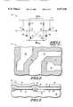
- FIG. 2includes a top view of a portion of a substrate including active and field isolation regions of a static-random-access memory cell.
- FIG. 3includes a cross-sectional view of a portion of the substrate of FIG. 2 after patterning a second conductive layer for a first time.
- FIG. 4includes a top view of the substrate of FIG. 3.
- FIG. 5includes a top view of the substrate of FIG. 4 after the latch gate electrodes and a word line have been formed.
- FIG. 6includes a cross-sectional view of the substrate of FIG. 5 after sidewall spacers and doped regions in the substrate have been formed.
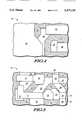
- FIG. 7includes a top view of the substrate of FIG. 6 after third conductive members have been formed.
- FIGS. 8 and 9include cross-sectional views of a portion of the substrate of FIG. 7 and portions of adjacent memory cells.
- FIG. 10includes a cross-sectional view of the substrate of FIG. 7 after the fabrication of the memory cell has been substantially completed.
- FIG. 11is similar to FIG. 8 except that FIG. 11 illustrates another embodiment of the present invention.
- FIG. 12includes a circuit diagram of a six-transistor static-random-access memory cell. (Prior art)
- the present inventionincludes an integrated circuit having a self-aligned contact that makes contact to both a region within the substrate and a capacitor plate of a capacitor that is adjacent to the region.
- the present inventionalso includes a static-random-access memory cell with a capacitor having a first plate and a second plate.
- the first plateincludes a first plate section of a gate electrode of a transistor
- the second plateincludes a second conductive member that is substantially coincident with the first plate section.
- the second plates of the capacitorsmay be formed over a portion of the gate electrode of a latch transistor or over a portion of a word line.
- the disclosureincludes methods of making the integrated circuit and the static-random-access memory cell.
- the present inventionincludes self-aligned contacts to doped regions adjacent the gate electrodes of latch and pass transistors.
- the self-aligned contactstypically reduce the likelihood of forming a short between a gate electrode and the contacts.
- the self-aligned contactsare also more likely to have a narrower distribution of contact resistances and have more process margin during their formation.
- the embodimentalso includes a static-random-access memory cell having "embedded" capacitors, which allow more charge to be stored within the gate electrodes of the latch transistors.
- the embedded capacitorsare formed in a self-aligned nature that allows their integration into an existing process flow while adding a minimum of extra processing steps to a conventional SRAM process flow.
- FIG. 1includes a circuit diagram of a four-transistor static-random-access memory cell 10.
- the memory cell 10includes a first storage node 17 and a second storage node 18.
- a first pass transistor 11, a first latch transistor 12, and a first load resistor 13are associated with the first storage node 17, and a second pass transistor 14, a second latch transistor 15, and a second load resistor 16 are associated with the second storage node 18.
- the gate electrode for the first latch transistor 12is electrically connected to the second storage node 18, and the gate electrode for the second latch transistor 15 is electrically connected to the first storage node 17.
- a first embedded capacitor 201has one plate electrically connected to the first storage node 17 and the other plate electrically connected to the V SS electrode.
- a second embedded capacitor 202has one plate electrically connected to the second storage node 18 and the other plate electrically connected to the V SS electrode.
- the gate electrodes for the pass transistors 11 and 14are part of a word line 19.
- a source/drain region of the first pass transistor 11is connected to a first bit line, and a source/drain region of the second pass transistor 14 is connected to a second bit line.
- the source regions of the latch transistors 12 and 15are electrically connected to one another and to the V SS electrode, which is at about ground potential when the memory cell is operating.
- the source regions of the load resistors 13 and 16are electrically connected to one another and to a V DD electrode, which is at a potential in a range of about 2-5 volts when the memory cell is operating.
- FIG. 2includes a top view of a portion of a lightly p-type doped monocrystalline silicon substrate (substrate) generally illustrating the area where the SRAM memory cell 10 is formed.
- the memory cell 10includes field isolation regions 21 and active regions 22 that lie within the substrate.
- a gate dielectric layer 31is formed to a thickness of about 150 angstroms by thermally growing silicon dioxide from silicon that lies within the active regions 22 of the substrate 30 as shown in FIG. 3.
- a relatively thin silicon layerabout 500 angstroms thick is formed by depositing silicon over the memory cell 10.
- the gate dielectric layer 31 and the relatively thin silicon layerare selectively etched using conventional lithographic and etching methods, so that an opening 35 is formed.
- a relatively thick silicon layer about 1500 angstroms thickis formed by depositing silicon over the memory cell 10 including within the opening 35.
- a heavy n-type doping stepis performed to make the relatively thin and relatively thick silicon layers conductive.
- the relatively thin and relatively thick silicon layersare referred to hereinafter as the first conductive layer 32. Referring to FIG. 3, the two layers are present over all of the memory cell except for opening 35, which only has the relatively thick silicon layer.
- An oxide-nitride-oxide (ONO) layer 33is formed over the memory cell 10 by thermally oxidizing the first conductive layer 32, depositing a silicon nitride layer over the thermal oxide, and annealing the deposited silicon nitride layer in an ambient including an oxidizing species.
- the thermally grown oxideis about 50 angstroms thick, and the deposited silicon nitride is about 100 angstroms thick.
- the thickness of the oxide layer formed during the annealing stepis difficult to determine.
- the annealing stepis generally long enough to fill any pinholes that may be present within the deposited silicon nitride layer.
- Some of the silicon nitride layermay be converted to silicon dioxide during the anneal.
- Formation of ONO layersis a conventional process and may be formed by those skilled in the art. During the formation of the ONO layer 33, some of the dopant from the first conductive layer 32 diffuses into the substrate 30 to form a buried contact region 36.
- a second conductive layer 34is formed by depositing silicon to a thickness of about 1800 angstroms and heavily doping the silicon with an n-type dopant to make the silicon conductive.
- the second conductive layer 34is patterned to remove some of the second conductive layer 34 from the memory cell 10 as shown in FIGS. 3 and 4.
- the first conductive layer 32is not shown in FIG. 4 to better illustrate the positional relationship between the second conductive layer and the field isolation regions 21 and the active regions 22.
- the gate dielectric layer 31 and the ONO layer 33are not illustrated within any of the top views of the figures of this specification in order to simplify illustrating the positional relationships between the various conductive layers with selected underlying layers.
- the second conductive layergenerally covers 1) all of the latch transistor regions of the memory cell except for locations where storage node areas are subsequently formed, and 2) strips over locations where portions of a word line and bit line contacts are subsequently formed.
- the uppermost layer of the memory cell 10includes the patterned second conductive layer 34 and exposed portions of the ONO layer 33.
- the first conductive, ONO, and second conductive layers 32-34are patterned in a self-aligned etching sequence including three steps to form latch gate electrodes and a word line as described below.
- a masking layer(not shown) is formed over the memory cell 10 and includes masking openings (not shown) that expose portions of the second conductive layer 34.
- the first etching stepetches the exposed portions of the second conductive layer 34 to form second conductive members 77 and 79 and exposes portions of the ONO layer 33.
- the second etching stepetches the exposed portions of the ONO layer 33 to expose portions of the first conductive layer 32.
- the third etching stepetches the exposed portions of the first conductive layer 32 to form latch gate electrodes 57 and a word line 59.
- the gate dielectric layer 31 or the field isolation regions 21act as an etch stop during the third etching step.
- the etching sequenceis performed on a conventional plasma etcher and conventional anisotropic etching methods.
- the first and third etching stepsboth use gases that include chlorine and hydrogen bromide
- the second etching stepuses gases that include trifluoro-methane and tetrafluoro-methane.
- gasesmay be used in place of or in conjunction with the gases listed above for the three etching steps. These other gases may include helium, for example.
- Selectivity of each of the etching stepsmay be changed by the using different gases, pressures, or techniques of exciting the gases that form the etching chemistries.
- the patterning of the three layersmay be performed during a plurality of separate etching sequences or using a plurality of etchers.
- Each latch gate electrode 57 or the word line 59comprises the first conductive layer 32 and is a conductive member.
- Each latch gate electrode 57consists of a main body section and a storage node section that includes a storage node area.
- Each main body section of the latch gate electrodes 57act as the gate electrodes for the latch transistors of the memory cell 10.
- each main body section of the latch gate electrodes 57acts as a first capacitor plate, too.
- the word line 59includes main body sections and connecting sections. Each main body section acts as a pass gate electrode for a pass transistor.
- each main body section of the word line 59acts as a first capacitor plate, too.
- the word line 59also includes connecting sections that lie adjacent to the main body sections and electrically connect the main body sections to form a single continuous word line 59 for the memory cell 10. One of the connecting sections is connected to a row decoder.
- Each second conductive member 77 or 79has an area substantially coincident with the main body sections of the latch gate electrodes 57 or of the word line 59. In this embodiment, each second conductive member 77 lies over only the main body sections and not over either the storage node sections or the storage node areas of the memory cell. As shown in FIG. 5, each second conductive member 77 or 79 does not significantly extend in any lateral direction beyond the edges of its respective underlying conductive member of the first conductive layer 32.
- Many other SRAM cells known in the arthave stacked capacitors with capacitor plates that cover at least the storage node areas of conductive members that also act as the gate electrodes for the latch transistors. Unlike these other SRAM cells, none of the capacitor plates of the embedded capacitors of the memory cell of this embodiment covers a storage node area.
- N-type regions 51are formed by ion implanting an n-type dopant, and the N-type regions 51 subsequently form lightly doped drain (LDD) regions of the pass and latch transistors.
- Sidewall spacers 52are formed by depositing about 2000 angstroms of silicon nitride and anisotropically etching the silicon nitride using conventional methods.
- the memory cellis heavily doped with an n-type dopant to form heavily doped regions 53 as seen in FIG. 6.
- FIGS. 7-9include illustrations of the memory cell after forming a couple of additional layers. Below is a brief explanation of the steps involved, and the subsequent paragraphs discuss the relationships between the layers in greater detail.
- a first insulating layer 73is formed over the memory cell 10 by depositing silicon dioxide to a thickness of about 1500 angstroms using an ambient including tetraethylorthosilicate (TEOS).
- TEOStetraethylorthosilicate
- the first insulating layer 73is patterned to expose portions of doped regions 81 that are adjacent to the latch gate electrodes 57 and the word line 59.
- the patterning stepalso exposes portions of the second conductive members 77 and 79.
- a third conductive layeris formed by depositing about 2500 angstroms of silicon and heavily doping the silicon with an n-type dopant to make the silicon conductive.
- the third conductive layeris patterned, and a refractory-metal silicide layer is formed over and from a part of the third conductive layer.
- Third conductive members 61 and 62include the patterned third conductive layer and the refractory-metal silicide layer. All steps performed within this paragraph are done using conventional methods.
- FIG. 7includes a top view of the memory cell 10, and FIGS. 8 and 9 are cross-sectional views through latch transistors and a bit line region, respectively. Thermal cycles since the time of forming the doped regions 51 and 53 have caused the doped regions to diffuse into one another to form doped regions 81 as seen in FIGS. 8 and 9. Similarly, buried contact region 36 and doped regions 51 and 53 have diffused together to form doped regions 82 in FIG. 9.
- FIG. 7includes a top view of the memory cell 10 after forming the third conductive member 61 and 62 and illustrates the positional relationship between the third conductive members 61 and 62 and other regions of the memory cell 10.
- FIG. 8includes a cross-sectional view of the memory cell taken along a direction that is substantially perpendicular to the length of the latch gate electrodes 57.
- the memory cell 10is typically one of a plurality of memory cells within a memory array.
- FIG. 8also includes a portion of memory cell 71, which is a memory cell that is located above and adjacent to memory cell 10 of FIG. 7.
- the memory cell 71has a memory cell layout that is a mirror image of the memory cell 10.
- the third conductive member 61contacts the doped region 81, which acts as the source region of the latch transistors shown in FIG. 8.
- the sidewall spacers 52 and the first insulating layer 73reduce the likelihood of an electrical short between the third conductive member 61 and both the latch gate electrodes 57 and drain regions of the latch transistors. Most of the capacitive coupling between the third conductive member 61 and the latch gate electrode 57 is contributed by the embedded capacitors. Although some capacitive coupling occurs between the third conductive member 61 and the latch gate electrodes 57 at the sidewall spacers 52, the capacitive coupling at the sidewall spacers 52 contributes little to the total capacitive coupling between the third conductive member 61 and the latch gate electrodes 57.
- the drain regions of the latch transistorsare doped regions 81 within the substrate 30 and are located along the opposing sides of the figure.
- FIG. 9is similar to FIG. 8 in that it illustrates how a third conductive member contacts second conductive members and a doped region within the substrate.
- FIG. 9includes a cross-sectional view of the memory cell taken along a direction that is substantially perpendicular to the length of the word line 59.
- FIG. 9also includes a portion of memory cell 101, which is a memory cell that is located to the right of and adjacent to memory cell 10 of FIG. 7.
- the memory cell 101has a memory cell layout that is a mirror image of the memory cell 10.
- the third conductive member 62contacts the doped region 81, which acts as a first source/drain region of the pass transistors shown in FIG. 9.
- the sidewall spacers 52 and the first insulating layer 73reduce the likelihood of forming an electrical short between the third conductive member 62 within the contact opening and the word lines 59.
- Most of the capacitive coupling between the third conductive members 62 and the word line 59is contributed by the embedded capacitors.
- the capacitive coupling at the sidewall spacers 52contributes little to the total capacitive coupling between the third conductive members 62 and the word line 59.
- Similar structuresare formed along other parts of the word lines 59.
- the third conductive member 62does not extend beyond the edges of the word lines 59 that are adjacent to the doped regions 82.
- a second insulating layer 91, a load resistor layer, a borophosphosilicate glass layer 93, contact openings and contacts 94, an interconnecting layer 95, and a passivation layer 96are formed to finish fabricating the memory cell as shown in FIG. 10. Conventional methods are used to form the layers, openings, contacts, and vias. If needed, additional insulating layers, via openings and vias, and additional interconnecting levels may be formed.
- the load resistor layercomprises silicon and includes resistor sections 921, storage node sections 922, and an electrode section 923.
- FIG. 10includes one of the resistor sections 921 and one of the storage node sections 922.
- the thickness, length, width, and doping level of the resistor sections 921generally determine the resistance of the load resistors.
- the resistor sectionis lightly n-type doped and has a resistance on the order of gigaohms.
- the electrode section 923is heavily doped to provide electrical contact to a V DD electrode, and the storage node sections 922 are heavily doped to provide electrical contact to the storage node areas of the storage node sections of the latch gate electrodes 57. It is pointed out that the cross-sectional view in FIG. 10 is along that portion one of the latch gate electrodes 57, wherein the portion is closer to the doped region 81 that acts as a source region for the latch transistor. (See FIG. 8.)
- FIG. 10illustrates the doped region 81 that is electrically connected to a first bit line (illustrated in FIG. 10 as the interconnecting layer 95 via the contact 94 and one of the third conductive members 62) that is electrically connected to a sense amplifier.
- a first bit lineillustrated in FIG. 10 as the interconnecting layer 95 via the contact 94 and one of the third conductive members 62
- another doped region 81 (not shown) that is also adjacent the word line 59is electrically connected to a second bit line (not shown) in a manner similar to the first bit line.
- the word line 59is connected to a row decoder (not shown).
- the doped regions 81that act as the source regions of the latch transistors (illustrated in FIG.
- the embodiment described aboveincludes many benefits.
- the capacitorsare formed prior to the formation of the load resistor layer and are hereinafter called “embedded” capacitors.
- the memory cell with the embedded capacitorstypically has a reduced soft-error rate compared to a conventional SRAM cell.
- the self-aligned nature of the formation of the plates for the embedded capacitorsallows their integration into an existing process flow while adding a minimum of extra processing steps.
- the embedded capacitorsare not formed after the load resistors are formed. Misalignment between the plates of a traditional stacked capacitor generally results in a wider distribution of capacitances between stacked capacitors.
- the self-aligned nature of forming the embedded capacitorsgenerally results in a narrow distribution of capacitances between the embedded capacitors.
- the embedded capacitorsare less likely to significantly change the topology of the memory cell. Therefore, the memory cell using embedded capacitors is less likely to cause an additional or more complicated planarization process sequence.
- the present inventionincludes self-aligned contacts to the doped regions 81 adjacent the latch gate electrodes 57 and the word line 59.
- the third conductive members 61 and 62include contact regions that are self-aligned to the source regions of the latch transistors or source/drain regions of the pass transistors.
- the self-aligned contactstypically reduce the likelihood of forming a short between a gate electrode and a contact to a doped region within the substrate.
- the self-aligned contactsare also more likely to have a narrower distribution of contact resistances.
- the third conductive members 61 and 62act as "landing pads" where contacts to others layers such as contacts 94 may be formed. Referring to FIG.
- the location of the contact 94may be moved so that it overlaps part of the word line 59 without significantly affecting the performance of the memory cell 10. Therefore, the embodiment of the Example has more process margin compared to an embodiment having contacts to a doped region within the substrate, where the contacts are not self-aligned.
- the memory cellmay be formed using a substrate that is a monocrystalline material or a substrate that includes a layer of the monocrystalline material over an insulating layer such as silicon dioxide or sapphire, wherein the monocrystalline material includes silicon, germanium, diamond, or III-V semiconductor materials such as gallium arsenide, for example.
- the conductivity types of the all doped layersmay be reversed.
- the gate dielectric layermay include silicon dioxide or silicon oxynitride.
- the insulating layers and sidewall spacersmay include silicon dioxide, silicon oxynitride, or silicon nitride.
- the ONO layermay be replaced by one or more insulating layers.
- a gate dielectric layer or an insulating layermay be thermally grown or deposited using silicon sources (such as TEOS, diethylsilane, silane, disilane, or chlorine-silicon compounds, etc.) and may be undoped or doped with boron or phosphorous dopants.
- the sidewall spacer materialis typically selected so that it is different from the material of a layer adjacent to which the sidewall spacer is formed. One skilled in the art is capable of selecting a sidewall spacer material.
- the conductive layersmay include doped silicon, a refractory metal or its silicide, a metal or a metal-containing compound, or a combination thereof.
- the silicon layersmay include epitaxial silicon, amorphous silicon, polycrystalline silicon (polysilicon), or a combination thereof.
- a refractory metal or its silicidemay comprise a material including titanium, tungsten, cobalt, molybdenum, tantalum, or the like.
- the metal or metal-containing compoundincludes aluminum, gold, copper, titanium nitride, tungsten, or the like.
- the metal or metal containing con, poundsmay also include a small amount of silicon.
- the memory cell of the embodiment of the Examplemay be used with design rules in a range of about 0.25-1.0 micron.
- design rulesmay be used with design rules lower than 0.25 micron or greater than 1.0 micron.
- the gate dielectric layerhas a thickness in a range of about 50-500 angstroms; each insulating layer has a thickness in a range of about 1500-4500 angstroms; and each deposited layer used to form the sidewall spacers has a thickness in a range of about 500-3000 angstroms.
- the relatively thin silicon layerhas a thickness in a range of about 200-1000 angstroms; the relatively thick silicon layer has a thickness in a range of about 1000-3000 angstroms; and each second or third conductive layer has a thickness in a range of about 500-4000 angstroms.
- the load resistorsmay have resistances on the order of megaohms to teraohms.
- the thickness of the ONO layermay be expressed as its electrically-measured oxide equivalent thickness.
- a composite layerincludes a silicon dioxide layer about 50 angstroms thick and a silicon nitride layer about 100 angstroms thick.
- the composite layermay have an electrically-measured oxide equivalent thickness of about 100 angstroms. Electrically-measured oxide equivalent thicknesses are known to one skilled in the art and are typically used in conjunction with composite insulating layers that include a plurality of electrically insulating materials such as silicon dioxide and silicon nitride.
- the ONO layer 33has an electrically-measured oxide equivalent thickness in a range of about 50-200 angstroms. The ranges of design rules, thicknesses, etc., are meant to be illustrative and not limiting.
- the second conductive members 77may be electrically connected to the V DD electrode.
- a patterned N + buried layermay be used to electrically connect the source regions of the latch transistors to the V SS electrode.
- the first insulating layer 73is patterned so that a portion of it remains over the doped region 111, which acts as the source regions for the latch transistors of memory cells 10 and 71, as shown in FIG. 11.
- the doped region 111is electrically connected to the V SS electrode (not shown) via the N + buried layer (not shown).
- the first insulating layer 73includes openings over the tops of the second conductive members 77.
- the third conductive member 61is deposited and contacts the second conductive members 77.
- the second insulating layer 91When the second insulating layer 91 is patterned, at least one opening (not shown) is formed to expose a portion of the third conductive member 61 that lies below the subsequently formed electrode section 923 of the load resistor layer. After the load resistor layer is formed, a portion of the electrode section 923 (not shown) of the load resistor layer contacts the second conductive member 61, and the electrode section 923 is electrically connected to a V DD electrode.
- the second conductive member 61may be electrically connected to V SS or V DD , one skilled in the art is capable of analyzing a memory cell layout to determine whether the third conductive member 61 is more easily electrically connected to the V SS or V DD electrode.
- a memory cellmay need the layout changed, whereas other memory cells do not require the layout to be change. It should be pointed out that a memory cell may have layout, wherein a single doped region within the memory cell (as opposed to two doped regions in the embodiment of the Example) acts as the source regions for the latch transistors, and the doped region would be electrically connected to the V SS electrode.
- an interconnecting line having a potentialwhich is a fraction of the V DD potential, is connected to the third conductive member 61 of FIG. 7. Integrating the electrical connection into the memory typically complicates the process flow, but may be done by one skilled in the art. Benefits of the embodiments of the present invention should be realized as long as the potential on the third conductive member 61 is relatively constant (independent of time).
- FIG. 12includes a circuit diagram of a six-transistor SRAM cell 120 that includes load transistors 123 and 126.
- the memory cell layout of the embodiment including the pattern of the second conductive member 61 of the embodiment of the Examplemay need to be modified in order to incorporate load transistors.
- the load transistorshave storage node sections contacting the storage node areas of the first latch gate electrodes 57 and have an electrode section electrically connected to a V DD electrode. If the load transistors are p-channel transistors, the storage node sections act as drain regions for the load transistors, and the electrode sections act as the source regions for the load transistors.
- the storage node sectionsact as source regions for the load transistors, and the electrode sections act as the drain regions for the load transistors.
- the third conductive membersmay be electrically connected to the drain regions of the latch transistors or the drain regions of the load transistors.
- the second conductive members 77may cover all of the latch gate electrodes 57 except the storage node areas, which are where the storage node ends of the load resistors contact the latch gate electrodes 57.
- Each second conductive member 77 and its underlying latch gate electrode 57are patterned so that they are substantially coincident with each other including over the storage node sections.
- the third conductive members 61 and 62are formed in a manner similar to the embodiment of the Example. After the second insulating layer 91 has been deposited, the second insulating layer 91, the second conductive members 77, and the ONO layers are etched to expose the storage node areas of the latch gate electrodes 57.
- Second sidewall spacersare formed within the openings by depositing about 500-2000 angstroms of silicon nitride and anisotropically etching the silicon nitride. After the second insulating layer 91 has been patterned and the second sidewalls spacers are formed, the load resistor layer is deposited. The rest of the processing described in the embodiment of the Example is the same for this embodiment. The second sidewall spacers prevent electrical connection between the second conductive members 77 and the load resistor layer. This embodiment has a higher storage node capacitance because part of the storage node section of the latch gate electrode 57 is covered, but the formation of the openings to the storage node areas and the sidewall spacers complicates the processing sequence.
- disposable sidewall spacersmay be used. After the latch gate electrodes 57 and word line 59 are formed by patterning the first conductive layer 32, the exposed sidewalls of the latch gate electrodes 57, word line 59, second conductive members 77 and 79 are thermally oxidized to form a protective oxide layer along their exposed sides. Processing continues substantially as described up through the patterning of the first insulating layer 73. After patterning the first insulating layer 73, the exposed sidewall spacers 52 are removed. Referring to FIGS. 8 and 9, the middle two sidewall spacers 52 are removed. An oxide layer is deposited and etched to form oxide sidewall spacers (not shown). The oxide sidewall spacers have virtually the same shape as the sidewall spacers 52.
- the protective oxide layer(not shown) helps to protect the latch gate electrodes 57, word line 59, and the second conductive members 61 and 62 during the formation of the oxide sidewall spacers.
- the oxide sidewall spacershelp to reduce capacitive coupling and charge accumulation within the sidewall spacers when compared to sidewall spacers 52 of the embodiment of the Example.
Landscapes
- Engineering & Computer Science (AREA)
- Microelectronics & Electronic Packaging (AREA)
- Computer Hardware Design (AREA)
- Semiconductor Memories (AREA)
Abstract
Description
Claims (19)
Priority Applications (2)
| Application Number | Priority Date | Filing Date | Title |
|---|---|---|---|
| US07/990,341US5377139A (en) | 1992-12-11 | 1992-12-11 | Process forming an integrated circuit |
| US08/278,465US5485420A (en) | 1992-12-11 | 1994-07-21 | Static-random-access memory cell and an integrated circuit having a static-random-access memory cell |
Applications Claiming Priority (1)
| Application Number | Priority Date | Filing Date | Title |
|---|---|---|---|
| US07/990,341US5377139A (en) | 1992-12-11 | 1992-12-11 | Process forming an integrated circuit |
Related Child Applications (1)
| Application Number | Title | Priority Date | Filing Date |
|---|---|---|---|
| US08/278,465DivisionUS5485420A (en) | 1992-12-11 | 1994-07-21 | Static-random-access memory cell and an integrated circuit having a static-random-access memory cell |
Publications (1)
| Publication Number | Publication Date |
|---|---|
| US5377139Atrue US5377139A (en) | 1994-12-27 |
Family
ID=25536055
Family Applications (2)
| Application Number | Title | Priority Date | Filing Date |
|---|---|---|---|
| US07/990,341Expired - LifetimeUS5377139A (en) | 1992-12-11 | 1992-12-11 | Process forming an integrated circuit |
| US08/278,465Expired - Fee RelatedUS5485420A (en) | 1992-12-11 | 1994-07-21 | Static-random-access memory cell and an integrated circuit having a static-random-access memory cell |
Family Applications After (1)
| Application Number | Title | Priority Date | Filing Date |
|---|---|---|---|
| US08/278,465Expired - Fee RelatedUS5485420A (en) | 1992-12-11 | 1994-07-21 | Static-random-access memory cell and an integrated circuit having a static-random-access memory cell |
Country Status (1)
| Country | Link |
|---|---|
| US (2) | US5377139A (en) |
Cited By (14)
| Publication number | Priority date | Publication date | Assignee | Title |
|---|---|---|---|---|
| US5488232A (en)* | 1993-09-28 | 1996-01-30 | North Carolina State University | Oriented diamond film structures on non-diamond substrates |
| US5541436A (en)* | 1994-01-07 | 1996-07-30 | The Regents Of The University Of Texas System | MOS transistor having improved oxynitride dielectric |
| US5610856A (en)* | 1995-03-07 | 1997-03-11 | Hitachi, Ltd. | Semiconductor integrated circuit device |
| US5700707A (en)* | 1996-06-13 | 1997-12-23 | Chartered Semiconductor Manufacturing Pte Ltd. | Method of manufacturing SRAM cell structure having a tunnel oxide capacitor |
| US6468855B2 (en) | 1998-08-14 | 2002-10-22 | Monolithic System Technology, Inc. | Reduced topography DRAM cell fabricated using a modified logic process and method for operating same |
| US6509595B1 (en)* | 1999-06-14 | 2003-01-21 | Monolithic System Technology, Inc. | DRAM cell fabricated using a modified logic process and method for operating same |
| US6573548B2 (en) | 1998-08-14 | 2003-06-03 | Monolithic System Technology, Inc. | DRAM cell having a capacitor structure fabricated partially in a cavity and method for operating same |
| US6611419B1 (en) | 2000-07-31 | 2003-08-26 | Intel Corporation | Electronic assembly comprising substrate with embedded capacitors |
| US20040090753A1 (en)* | 1999-09-02 | 2004-05-13 | Kabushiki Kaisha Toshiba | Component mounting circuit board with resin-molded section covering circuit pattern and inner components |
| US6775150B1 (en) | 2000-08-30 | 2004-08-10 | Intel Corporation | Electronic assembly comprising ceramic/organic hybrid substrate with embedded capacitors and methods of manufacture |
| US6825091B2 (en)* | 2000-01-26 | 2004-11-30 | Samsung Electronics Co., Ltd. | Semiconductor memory device and method of manufacturing same |
| US6970362B1 (en) | 2000-07-31 | 2005-11-29 | Intel Corporation | Electronic assemblies and systems comprising interposer with embedded capacitors |
| US20060113547A1 (en)* | 2004-11-29 | 2006-06-01 | Samsung Electronics Co., Ltd. | Methods of fabricating memory devices including fuses and load resistors in a peripheral circuit region |
| US20060172504A1 (en)* | 2005-02-03 | 2006-08-03 | Monolithic System Technology, Inc. | Fabrication process for increased capacitance in an embedded DRAM memory |
Families Citing this family (37)
| Publication number | Priority date | Publication date | Assignee | Title |
|---|---|---|---|---|
| KR0135801B1 (en)* | 1994-07-26 | 1998-04-24 | 김광호 | Static random access memory device and the method of making it |
| DE19781675B4 (en)* | 1996-03-28 | 2006-08-24 | Intel Corporation, Santa Clara | Memory cell design with vertically stacked crossings |
| US5674770A (en)* | 1996-09-27 | 1997-10-07 | Taiwan Semiconductor Manufacturing Company, Ltd. | Method of fabricating an SRAM device with a self-aligned thin film transistor structure |
| JPH10229135A (en) | 1997-02-14 | 1998-08-25 | Mitsubishi Electric Corp | Semiconductor device and manufacturing method thereof |
| US6174764B1 (en)* | 1997-05-12 | 2001-01-16 | Micron Technology, Inc. | Process for manufacturing integrated circuit SRAM |
| JP3567081B2 (en)* | 1997-05-30 | 2004-09-15 | ルーセント テクノロジーズ インコーポレーテッド | SRAM device and method of manufacturing the same |
| JP3384714B2 (en)* | 1997-07-16 | 2003-03-10 | 富士通株式会社 | Semiconductor device and manufacturing method thereof |
| JP3134927B2 (en)* | 1998-05-01 | 2001-02-13 | 日本電気株式会社 | Semiconductor device and method of manufacturing SRAM cell |
| ATE249090T1 (en)* | 1998-06-05 | 2003-09-15 | Bae Systems Information | RADIATION PROTECTED 6-TRANSISTOR MEMORY WITH RANDOM ACCESS AND MEMORY COMPONENT |
| US6243286B1 (en)* | 1998-07-27 | 2001-06-05 | Seiko Epson Corporation | Semiconductor memory device and method of fabricating the same |
| US6038163A (en)* | 1998-11-09 | 2000-03-14 | Lucent Technologies Inc. | Capacitor loaded memory cell |
| US6668342B2 (en) | 2000-04-28 | 2003-12-23 | Bae Systems Information And Electronic Systems Integration, Inc. | Apparatus for a radiation hardened clock splitter |
| US8357435B2 (en)* | 2008-05-09 | 2013-01-22 | Applied Materials, Inc. | Flowable dielectric equipment and processes |
| US20100081293A1 (en)* | 2008-10-01 | 2010-04-01 | Applied Materials, Inc. | Methods for forming silicon nitride based film or silicon carbon based film |
| US8511281B2 (en)* | 2009-07-10 | 2013-08-20 | Tula Technology, Inc. | Skip fire engine control |
| US8980382B2 (en)* | 2009-12-02 | 2015-03-17 | Applied Materials, Inc. | Oxygen-doping for non-carbon radical-component CVD films |
| US8741788B2 (en)* | 2009-08-06 | 2014-06-03 | Applied Materials, Inc. | Formation of silicon oxide using non-carbon flowable CVD processes |
| US8449942B2 (en)* | 2009-11-12 | 2013-05-28 | Applied Materials, Inc. | Methods of curing non-carbon flowable CVD films |
| JP2013516763A (en) | 2009-12-30 | 2013-05-13 | アプライド マテリアルズ インコーポレイテッド | Dielectric film growth using radicals generated using a flexible nitrogen / hydrogen ratio |
| US20110159213A1 (en)* | 2009-12-30 | 2011-06-30 | Applied Materials, Inc. | Chemical vapor deposition improvements through radical-component modification |
| US8329262B2 (en)* | 2010-01-05 | 2012-12-11 | Applied Materials, Inc. | Dielectric film formation using inert gas excitation |
| SG182336A1 (en)* | 2010-01-06 | 2012-08-30 | Applied Materials Inc | Flowable dielectric using oxide liner |
| KR101837648B1 (en) | 2010-01-07 | 2018-04-19 | 어플라이드 머티어리얼스, 인코포레이티드 | Insitu ozone cure for radicalcomponent cvd |
| JP2013521650A (en) | 2010-03-05 | 2013-06-10 | アプライド マテリアルズ インコーポレイテッド | Conformal layer by radical component CVD |
| US9285168B2 (en) | 2010-10-05 | 2016-03-15 | Applied Materials, Inc. | Module for ozone cure and post-cure moisture treatment |
| US8664127B2 (en) | 2010-10-15 | 2014-03-04 | Applied Materials, Inc. | Two silicon-containing precursors for gapfill enhancing dielectric liner |
| US10283321B2 (en) | 2011-01-18 | 2019-05-07 | Applied Materials, Inc. | Semiconductor processing system and methods using capacitively coupled plasma |
| US8450191B2 (en) | 2011-01-24 | 2013-05-28 | Applied Materials, Inc. | Polysilicon films by HDP-CVD |
| US8716154B2 (en) | 2011-03-04 | 2014-05-06 | Applied Materials, Inc. | Reduced pattern loading using silicon oxide multi-layers |
| US8445078B2 (en) | 2011-04-20 | 2013-05-21 | Applied Materials, Inc. | Low temperature silicon oxide conversion |
| US8466073B2 (en) | 2011-06-03 | 2013-06-18 | Applied Materials, Inc. | Capping layer for reduced outgassing |
| US9404178B2 (en) | 2011-07-15 | 2016-08-02 | Applied Materials, Inc. | Surface treatment and deposition for reduced outgassing |
| US8617989B2 (en) | 2011-09-26 | 2013-12-31 | Applied Materials, Inc. | Liner property improvement |
| US8551891B2 (en) | 2011-10-04 | 2013-10-08 | Applied Materials, Inc. | Remote plasma burn-in |
| US8889566B2 (en) | 2012-09-11 | 2014-11-18 | Applied Materials, Inc. | Low cost flowable dielectric films |
| US9018108B2 (en) | 2013-01-25 | 2015-04-28 | Applied Materials, Inc. | Low shrinkage dielectric films |
| US9412581B2 (en) | 2014-07-16 | 2016-08-09 | Applied Materials, Inc. | Low-K dielectric gapfill by flowable deposition |
Citations (17)
| Publication number | Priority date | Publication date | Assignee | Title |
|---|---|---|---|---|
| US4355455A (en)* | 1979-07-19 | 1982-10-26 | National Semiconductor Corporation | Method of manufacture for self-aligned floating gate memory cell |
| US4532609A (en)* | 1982-06-15 | 1985-07-30 | Tokyo Shibaura Denki Kabushiki Kaisha | Semiconductor memory device |
| US4535426A (en)* | 1982-07-19 | 1985-08-13 | Tokyo Shibaura Denki Kabushiki Kaisha | Semiconductor memory device |
| US4590508A (en)* | 1980-01-29 | 1986-05-20 | Nippon Electric Co., Ltd. | MOS static ram with capacitively loaded gates to prevent alpha soft errors |
| US4679171A (en)* | 1985-02-07 | 1987-07-07 | Visic, Inc. | MOS/CMOS memory cell |
| US4725981A (en)* | 1986-02-03 | 1988-02-16 | Motorola, Inc. | Random access memory cell resistant to inadvertant change of state due to charged particles |
| US4729002A (en)* | 1980-09-24 | 1988-03-01 | Semiconductor Energy Laboratory Co., Ltd. | Self-aligned sidewall gate IGFET |
| US4805147A (en)* | 1985-06-10 | 1989-02-14 | Hitachi, Ltd. | Stacked static random access memory cell having capacitor |
| US4805148A (en)* | 1985-11-22 | 1989-02-14 | Diehl Nagle Sherra E | High impendance-coupled CMOS SRAM for improved single event immunity |
| US4879690A (en)* | 1987-09-07 | 1989-11-07 | Mitsubishi Denki Kabushiki Kaisha | Static random access memory with reduced soft error rate |
| US5073510A (en)* | 1990-07-30 | 1991-12-17 | Samsung Electronics Co., Ltd. | Fabrication method of contact window in semiconductor device |
| EP0475688A2 (en)* | 1990-09-05 | 1992-03-18 | Sharp Kabushiki Kaisha | Method for manufacturing memories with thin film transistors |
| US5132771A (en)* | 1985-12-27 | 1992-07-21 | Hitachi, Ltd. | Semiconductor memory device having flip-flop circuits |
| US5135881A (en)* | 1990-09-27 | 1992-08-04 | Nec Corporation | Method of making random access memory device having memory cells each implemented by a stacked storage capacitor and a transfer transistor with lightly-doped drain structure |
| US5145799A (en)* | 1991-01-30 | 1992-09-08 | Texas Instruments Incorporated | Stacked capacitor SRAM cell |
| US5240872A (en)* | 1990-05-02 | 1993-08-31 | Mitsubishi Denki Kabushiki Kaisha | Method of manufacturing semiconductor device having interconnection layer contacting source/drain regions |
| US5264391A (en)* | 1991-02-28 | 1993-11-23 | Hyundai Electronics Industries Co., Ltd. | Method of forming a self-aligned contact utilizing a polysilicon layer |
- 1992
- 1992-12-11USUS07/990,341patent/US5377139A/ennot_activeExpired - Lifetime
- 1994
- 1994-07-21USUS08/278,465patent/US5485420A/ennot_activeExpired - Fee Related
Patent Citations (17)
| Publication number | Priority date | Publication date | Assignee | Title |
|---|---|---|---|---|
| US4355455A (en)* | 1979-07-19 | 1982-10-26 | National Semiconductor Corporation | Method of manufacture for self-aligned floating gate memory cell |
| US4590508A (en)* | 1980-01-29 | 1986-05-20 | Nippon Electric Co., Ltd. | MOS static ram with capacitively loaded gates to prevent alpha soft errors |
| US4729002A (en)* | 1980-09-24 | 1988-03-01 | Semiconductor Energy Laboratory Co., Ltd. | Self-aligned sidewall gate IGFET |
| US4532609A (en)* | 1982-06-15 | 1985-07-30 | Tokyo Shibaura Denki Kabushiki Kaisha | Semiconductor memory device |
| US4535426A (en)* | 1982-07-19 | 1985-08-13 | Tokyo Shibaura Denki Kabushiki Kaisha | Semiconductor memory device |
| US4679171A (en)* | 1985-02-07 | 1987-07-07 | Visic, Inc. | MOS/CMOS memory cell |
| US4805147A (en)* | 1985-06-10 | 1989-02-14 | Hitachi, Ltd. | Stacked static random access memory cell having capacitor |
| US4805148A (en)* | 1985-11-22 | 1989-02-14 | Diehl Nagle Sherra E | High impendance-coupled CMOS SRAM for improved single event immunity |
| US5132771A (en)* | 1985-12-27 | 1992-07-21 | Hitachi, Ltd. | Semiconductor memory device having flip-flop circuits |
| US4725981A (en)* | 1986-02-03 | 1988-02-16 | Motorola, Inc. | Random access memory cell resistant to inadvertant change of state due to charged particles |
| US4879690A (en)* | 1987-09-07 | 1989-11-07 | Mitsubishi Denki Kabushiki Kaisha | Static random access memory with reduced soft error rate |
| US5240872A (en)* | 1990-05-02 | 1993-08-31 | Mitsubishi Denki Kabushiki Kaisha | Method of manufacturing semiconductor device having interconnection layer contacting source/drain regions |
| US5073510A (en)* | 1990-07-30 | 1991-12-17 | Samsung Electronics Co., Ltd. | Fabrication method of contact window in semiconductor device |
| EP0475688A2 (en)* | 1990-09-05 | 1992-03-18 | Sharp Kabushiki Kaisha | Method for manufacturing memories with thin film transistors |
| US5135881A (en)* | 1990-09-27 | 1992-08-04 | Nec Corporation | Method of making random access memory device having memory cells each implemented by a stacked storage capacitor and a transfer transistor with lightly-doped drain structure |
| US5145799A (en)* | 1991-01-30 | 1992-09-08 | Texas Instruments Incorporated | Stacked capacitor SRAM cell |
| US5264391A (en)* | 1991-02-28 | 1993-11-23 | Hyundai Electronics Industries Co., Ltd. | Method of forming a self-aligned contact utilizing a polysilicon layer |
Non-Patent Citations (8)
| Title |
|---|
| Chappell, et al.; "Stability and SER Analysis of Static RAM Cells"; IEEE Trans. on Electron Dev.; vol. ED-32, No. 2, pp. 463-470 (1985). |
| Chappell, et al.; Stability and SER Analysis of Static RAM Cells ; IEEE Trans. on Electron Dev.; vol. ED 32, No. 2, pp. 463 470 (1985).* |
| Itabashi, et al.; "A Split Wordline Cell for 16Mb SRAM Using Polysilicon Sidewall Contacts"; IEDM; pp. 477-480 (1991). |
| Itabashi, et al.; A Split Wordline Cell for 16Mb SRAM Using Polysilicon Sidewall Contacts ; IEDM; pp. 477 480 (1991).* |
| Wang; "High Performance, High Density Capacitively Loaded FET Static RAM"; IBM Tech. Discl. Bulletin; vol. 27, No. 4A; pp. 1950-1951 (1984). |
| Wang; High Performance, High Density Capacitively Loaded FET Static RAM ; IBM Tech. Discl. Bulletin; vol. 27, No. 4A; pp. 1950 1951 (1984).* |
| Yamanaka, et al.; "A 25 μm2, New Poly-Si PMOS Load (PPL) SRAM Cell Having Excellent Soft Error Immunity"; IEDM; pp. 48-51 (1988). |
| Yamanaka, et al.; A 25 m2, New Poly Si PMOS Load (PPL) SRAM Cell Having Excellent Soft Error Immunity ; IEDM; pp. 48 51 (1988).* |
Cited By (29)
| Publication number | Priority date | Publication date | Assignee | Title |
|---|---|---|---|---|
| US5488232A (en)* | 1993-09-28 | 1996-01-30 | North Carolina State University | Oriented diamond film structures on non-diamond substrates |
| US5541436A (en)* | 1994-01-07 | 1996-07-30 | The Regents Of The University Of Texas System | MOS transistor having improved oxynitride dielectric |
| US5610856A (en)* | 1995-03-07 | 1997-03-11 | Hitachi, Ltd. | Semiconductor integrated circuit device |
| US5700707A (en)* | 1996-06-13 | 1997-12-23 | Chartered Semiconductor Manufacturing Pte Ltd. | Method of manufacturing SRAM cell structure having a tunnel oxide capacitor |
| US5825684A (en)* | 1996-06-13 | 1998-10-20 | Chartered Semiconductor Manufactuing, Ltd. | Sram cell structure |
| US6642098B2 (en) | 1998-08-14 | 2003-11-04 | Monolithic System Technology, Inc. | DRAM cell having a capacitor structure fabricated partially in a cavity and method for operating same |
| US6744676B2 (en) | 1998-08-14 | 2004-06-01 | Monolithic System Technology, Inc. | DRAM cell having a capacitor structure fabricated partially in a cavity and method for operating same |
| US6573548B2 (en) | 1998-08-14 | 2003-06-03 | Monolithic System Technology, Inc. | DRAM cell having a capacitor structure fabricated partially in a cavity and method for operating same |
| US6784048B2 (en) | 1998-08-14 | 2004-08-31 | Monolithic Systems Technology, Inc. | Method of fabricating a DRAM cell having a thin dielectric access transistor and a thick dielectric storage |
| US6468855B2 (en) | 1998-08-14 | 2002-10-22 | Monolithic System Technology, Inc. | Reduced topography DRAM cell fabricated using a modified logic process and method for operating same |
| US6654295B2 (en) | 1998-08-14 | 2003-11-25 | Monolithic System Technology, Inc. | Reduced topography DRAM cell fabricated using a modified logic process and method for operating same |
| US20030001181A1 (en)* | 1998-08-14 | 2003-01-02 | Monolithic System Technology, Inc. | Method of fabricating a DRAM cell having a thin dielectric access transistor and a thick dielectric storage capacitor |
| US6509595B1 (en)* | 1999-06-14 | 2003-01-21 | Monolithic System Technology, Inc. | DRAM cell fabricated using a modified logic process and method for operating same |
| US20040090753A1 (en)* | 1999-09-02 | 2004-05-13 | Kabushiki Kaisha Toshiba | Component mounting circuit board with resin-molded section covering circuit pattern and inner components |
| US7203071B2 (en) | 1999-09-02 | 2007-04-10 | Kabushiki Kaisha Toshiba | Component mounting circuit board with resin-molded section covering circuit pattern and inner components |
| US6825091B2 (en)* | 2000-01-26 | 2004-11-30 | Samsung Electronics Co., Ltd. | Semiconductor memory device and method of manufacturing same |
| US6611419B1 (en) | 2000-07-31 | 2003-08-26 | Intel Corporation | Electronic assembly comprising substrate with embedded capacitors |
| US7339798B2 (en) | 2000-07-31 | 2008-03-04 | Intel Corporation | Electronic assemblies and systems comprising interposer with embedded capacitors |
| US6970362B1 (en) | 2000-07-31 | 2005-11-29 | Intel Corporation | Electronic assemblies and systems comprising interposer with embedded capacitors |
| US20060012966A1 (en)* | 2000-07-31 | 2006-01-19 | Intel Corporation | Electronic assemblies and systems comprising interposer with embedded capacitors |
| US6775150B1 (en) | 2000-08-30 | 2004-08-10 | Intel Corporation | Electronic assembly comprising ceramic/organic hybrid substrate with embedded capacitors and methods of manufacture |
| US7120031B2 (en) | 2000-08-30 | 2006-10-10 | Intel Corporation | Data processing system comprising ceramic/organic hybrid substrate with embedded capacitors |
| US20060279940A1 (en)* | 2000-08-30 | 2006-12-14 | Intel Corporation | Electronic assemblies comprising ceramic/organic hybrid substrate with embedded capacitors |
| US20040238942A1 (en)* | 2000-08-30 | 2004-12-02 | Intel Corporation | Electronic assembly comprising ceramic/organic hybrid substrate with embedded capacitors and methods of manufacture |
| US7535728B2 (en) | 2000-08-30 | 2009-05-19 | Intel Corporation | Electronic assemblies comprising ceramic/organic hybrid substrate with embedded capacitors |
| US20060113547A1 (en)* | 2004-11-29 | 2006-06-01 | Samsung Electronics Co., Ltd. | Methods of fabricating memory devices including fuses and load resistors in a peripheral circuit region |
| US20060172504A1 (en)* | 2005-02-03 | 2006-08-03 | Monolithic System Technology, Inc. | Fabrication process for increased capacitance in an embedded DRAM memory |
| US7323379B2 (en) | 2005-02-03 | 2008-01-29 | Mosys, Inc. | Fabrication process for increased capacitance in an embedded DRAM memory |
| US20080093645A1 (en)* | 2005-02-03 | 2008-04-24 | Mosys, Inc. | Fabrication Process For Increased Capacitance In An Embedded DRAM Memory |
Also Published As
| Publication number | Publication date |
|---|---|
| US5485420A (en) | 1996-01-16 |
Similar Documents
| Publication | Publication Date | Title |
|---|---|---|
| US5377139A (en) | Process forming an integrated circuit | |
| US5536674A (en) | Process for forming a static-random-access memory cell | |
| US5744384A (en) | Semiconductor structures which incorporate thin film transistors | |
| US5843816A (en) | Integrated self-aligned butt contact process flow and structure for six transistor full complementary metal oxide semiconductor static random access memory cell | |
| US7560353B2 (en) | Methods of fabricating memory devices with memory cell transistors having gate sidewall spacers with different dielectric properties | |
| EP0562207B1 (en) | Method of forming thin film pseudo-planar PFET devices and structures resulting therefrom | |
| EP0523830B1 (en) | A stacked CMOS SRAM cell with polysilicon transistor load | |
| US6100128A (en) | Process for making six-transistor SRAM cell local interconnect structure | |
| US5330929A (en) | Method of making a six transistor static random access memory cell | |
| US20060019488A1 (en) | Method of forming a static random access memory with a buried local interconnect | |
| US20020030213A1 (en) | Semiconductor integrated circuit device and process for manufacturing the same | |
| EP0460833B1 (en) | Method of fabricating a field effect device with polycrystaline silicon channel | |
| US20030139027A1 (en) | Semiconductor integrated circuit device and a method of manufacturing the same | |
| JPH04237132A (en) | Semiconductor structure with polysilicon-land and forming method thereof | |
| US6534805B1 (en) | SRAM cell design | |
| JP7532730B2 (en) | SRAM cell structure | |
| US20040175919A1 (en) | Borderless contact structure and method of forming the same | |
| US6437455B2 (en) | Semiconductor device having gate-gate, drain-drain, and drain-gate connecting layers and method of fabricating the same | |
| US5824579A (en) | Method of forming shared contact structure | |
| US6900513B2 (en) | Semiconductor memory device and manufacturing method thereof | |
| US5497022A (en) | Semiconductor device and a method of manufacturing thereof | |
| US20220319567A1 (en) | Fft-dram | |
| JPH08288473A (en) | Semiconductor memory and its manufacture | |
| US5814868A (en) | Transistor having an offset channel section | |
| US5652174A (en) | Unified stacked contact process for static random access memory (SRAM) having polysilicon load resistors |
Legal Events
| Date | Code | Title | Description |
|---|---|---|---|
| AS | Assignment | Owner name:MOTOROLA, INC., ILLINOIS Free format text:ASSIGNMENT OF ASSIGNORS INTEREST.;ASSIGNORS:LAGE, CRAIG S.;BAKER, FRANK K.;HAYDEN, JAMES D.;AND OTHERS;REEL/FRAME:006360/0014 Effective date:19921210 | |
| STCF | Information on status: patent grant | Free format text:PATENTED CASE | |
| CC | Certificate of correction | ||
| FPAY | Fee payment | Year of fee payment:4 | |
| FPAY | Fee payment | Year of fee payment:8 | |
| AS | Assignment | Owner name:FREESCALE SEMICONDUCTOR, INC., TEXAS Free format text:ASSIGNMENT OF ASSIGNORS INTEREST;ASSIGNOR:MOTOROLA, INC.;REEL/FRAME:015698/0657 Effective date:20040404 Owner name:FREESCALE SEMICONDUCTOR, INC.,TEXAS Free format text:ASSIGNMENT OF ASSIGNORS INTEREST;ASSIGNOR:MOTOROLA, INC.;REEL/FRAME:015698/0657 Effective date:20040404 | |
| FPAY | Fee payment | Year of fee payment:12 | |
| AS | Assignment | Owner name:CITIBANK, N.A. AS COLLATERAL AGENT, NEW YORK Free format text:SECURITY AGREEMENT;ASSIGNORS:FREESCALE SEMICONDUCTOR, INC.;FREESCALE ACQUISITION CORPORATION;FREESCALE ACQUISITION HOLDINGS CORP.;AND OTHERS;REEL/FRAME:018855/0129 Effective date:20061201 Owner name:CITIBANK, N.A. AS COLLATERAL AGENT,NEW YORK Free format text:SECURITY AGREEMENT;ASSIGNORS:FREESCALE SEMICONDUCTOR, INC.;FREESCALE ACQUISITION CORPORATION;FREESCALE ACQUISITION HOLDINGS CORP.;AND OTHERS;REEL/FRAME:018855/0129 Effective date:20061201 | |
| AS | Assignment | Owner name:CITIBANK, N.A., AS COLLATERAL AGENT,NEW YORK Free format text:SECURITY AGREEMENT;ASSIGNOR:FREESCALE SEMICONDUCTOR, INC.;REEL/FRAME:024397/0001 Effective date:20100413 Owner name:CITIBANK, N.A., AS COLLATERAL AGENT, NEW YORK Free format text:SECURITY AGREEMENT;ASSIGNOR:FREESCALE SEMICONDUCTOR, INC.;REEL/FRAME:024397/0001 Effective date:20100413 | |
| AS | Assignment | Owner name:ZOZO MANAGEMENT, LLC, DELAWARE Free format text:ASSIGNMENT OF ASSIGNORS INTEREST;ASSIGNOR:FREESCALE SEMICONDUCTOR, INC.;REEL/FRAME:034034/0236 Effective date:20120814 | |
| AS | Assignment | Owner name:APPLE INC., CALIFORNIA Free format text:ASSIGNMENT OF ASSIGNORS INTEREST;ASSIGNOR:ZOZO MANAGEMENT, LLC;REEL/FRAME:034732/0019 Effective date:20141219 | |
| AS | Assignment | Owner name:FREESCALE SEMICONDUCTOR, INC., TEXAS Free format text:PATENT RELEASE;ASSIGNOR:CITIBANK, N.A., AS COLLATERAL AGENT;REEL/FRAME:037356/0143 Effective date:20151207 Owner name:FREESCALE SEMICONDUCTOR, INC., TEXAS Free format text:PATENT RELEASE;ASSIGNOR:CITIBANK, N.A., AS COLLATERAL AGENT;REEL/FRAME:037356/0553 Effective date:20151207 Owner name:FREESCALE SEMICONDUCTOR, INC., TEXAS Free format text:PATENT RELEASE;ASSIGNOR:CITIBANK, N.A., AS COLLATERAL AGENT;REEL/FRAME:037354/0225 Effective date:20151207 |