US5376591A - Method for manufacturing semiconductor device - Google Patents
Method for manufacturing semiconductor deviceDownload PDFInfo
- Publication number
- US5376591A US5376591AUS07/895,472US89547292AUS5376591AUS 5376591 AUS5376591 AUS 5376591AUS 89547292 AUS89547292 AUS 89547292AUS 5376591 AUS5376591 AUS 5376591A
- Authority
- US
- United States
- Prior art keywords
- film
- insulating film
- gas
- accordance
- manufacturing
- Prior art date
- Legal status (The legal status is an assumption and is not a legal conclusion. Google has not performed a legal analysis and makes no representation as to the accuracy of the status listed.)
- Expired - Fee Related
Links
Images


Classifications
- H—ELECTRICITY
- H01—ELECTRIC ELEMENTS
- H01L—SEMICONDUCTOR DEVICES NOT COVERED BY CLASS H10
- H01L21/00—Processes or apparatus adapted for the manufacture or treatment of semiconductor or solid state devices or of parts thereof
- H01L21/02—Manufacture or treatment of semiconductor devices or of parts thereof
- H01L21/02104—Forming layers
- H01L21/02107—Forming insulating materials on a substrate
- H01L21/02109—Forming insulating materials on a substrate characterised by the type of layer, e.g. type of material, porous/non-porous, pre-cursors, mixtures or laminates
- H01L21/02112—Forming insulating materials on a substrate characterised by the type of layer, e.g. type of material, porous/non-porous, pre-cursors, mixtures or laminates characterised by the material of the layer
- H01L21/02123—Forming insulating materials on a substrate characterised by the type of layer, e.g. type of material, porous/non-porous, pre-cursors, mixtures or laminates characterised by the material of the layer the material containing silicon
- H01L21/02164—Forming insulating materials on a substrate characterised by the type of layer, e.g. type of material, porous/non-porous, pre-cursors, mixtures or laminates characterised by the material of the layer the material containing silicon the material being a silicon oxide, e.g. SiO2
- H—ELECTRICITY
- H01—ELECTRIC ELEMENTS
- H01L—SEMICONDUCTOR DEVICES NOT COVERED BY CLASS H10
- H01L21/00—Processes or apparatus adapted for the manufacture or treatment of semiconductor or solid state devices or of parts thereof
- H01L21/02—Manufacture or treatment of semiconductor devices or of parts thereof
- H01L21/02104—Forming layers
- H01L21/02107—Forming insulating materials on a substrate
- H01L21/02225—Forming insulating materials on a substrate characterised by the process for the formation of the insulating layer
- H01L21/0226—Forming insulating materials on a substrate characterised by the process for the formation of the insulating layer formation by a deposition process
- H01L21/02263—Forming insulating materials on a substrate characterised by the process for the formation of the insulating layer formation by a deposition process deposition from the gas or vapour phase
- H01L21/02271—Forming insulating materials on a substrate characterised by the process for the formation of the insulating layer formation by a deposition process deposition from the gas or vapour phase deposition by decomposition or reaction of gaseous or vapour phase compounds, i.e. chemical vapour deposition
- H01L21/0228—Forming insulating materials on a substrate characterised by the process for the formation of the insulating layer formation by a deposition process deposition from the gas or vapour phase deposition by decomposition or reaction of gaseous or vapour phase compounds, i.e. chemical vapour deposition deposition by cyclic CVD, e.g. ALD, ALE, pulsed CVD
- H—ELECTRICITY
- H01—ELECTRIC ELEMENTS
- H01L—SEMICONDUCTOR DEVICES NOT COVERED BY CLASS H10
- H01L21/00—Processes or apparatus adapted for the manufacture or treatment of semiconductor or solid state devices or of parts thereof
- H01L21/02—Manufacture or treatment of semiconductor devices or of parts thereof
- H01L21/02104—Forming layers
- H01L21/02107—Forming insulating materials on a substrate
- H01L21/02296—Forming insulating materials on a substrate characterised by the treatment performed before or after the formation of the layer
- H01L21/02318—Forming insulating materials on a substrate characterised by the treatment performed before or after the formation of the layer post-treatment
- H01L21/02337—Forming insulating materials on a substrate characterised by the treatment performed before or after the formation of the layer post-treatment treatment by exposure to a gas or vapour
- H01L21/0234—Forming insulating materials on a substrate characterised by the treatment performed before or after the formation of the layer post-treatment treatment by exposure to a gas or vapour treatment by exposure to a plasma
- H—ELECTRICITY
- H01—ELECTRIC ELEMENTS
- H01L—SEMICONDUCTOR DEVICES NOT COVERED BY CLASS H10
- H01L21/00—Processes or apparatus adapted for the manufacture or treatment of semiconductor or solid state devices or of parts thereof
- H01L21/02—Manufacture or treatment of semiconductor devices or of parts thereof
- H01L21/04—Manufacture or treatment of semiconductor devices or of parts thereof the devices having potential barriers, e.g. a PN junction, depletion layer or carrier concentration layer
- H01L21/18—Manufacture or treatment of semiconductor devices or of parts thereof the devices having potential barriers, e.g. a PN junction, depletion layer or carrier concentration layer the devices having semiconductor bodies comprising elements of Group IV of the Periodic Table or AIIIBV compounds with or without impurities, e.g. doping materials
- H01L21/30—Treatment of semiconductor bodies using processes or apparatus not provided for in groups H01L21/20 - H01L21/26
- H01L21/31—Treatment of semiconductor bodies using processes or apparatus not provided for in groups H01L21/20 - H01L21/26 to form insulating layers thereon, e.g. for masking or by using photolithographic techniques; After treatment of these layers; Selection of materials for these layers
- H01L21/3105—After-treatment
- H—ELECTRICITY
- H01—ELECTRIC ELEMENTS
- H01L—SEMICONDUCTOR DEVICES NOT COVERED BY CLASS H10
- H01L21/00—Processes or apparatus adapted for the manufacture or treatment of semiconductor or solid state devices or of parts thereof
- H01L21/02—Manufacture or treatment of semiconductor devices or of parts thereof
- H01L21/02104—Forming layers
- H01L21/02107—Forming insulating materials on a substrate
- H01L21/02109—Forming insulating materials on a substrate characterised by the type of layer, e.g. type of material, porous/non-porous, pre-cursors, mixtures or laminates
- H01L21/02112—Forming insulating materials on a substrate characterised by the type of layer, e.g. type of material, porous/non-porous, pre-cursors, mixtures or laminates characterised by the material of the layer
- H01L21/02123—Forming insulating materials on a substrate characterised by the type of layer, e.g. type of material, porous/non-porous, pre-cursors, mixtures or laminates characterised by the material of the layer the material containing silicon
- H01L21/02126—Forming insulating materials on a substrate characterised by the type of layer, e.g. type of material, porous/non-porous, pre-cursors, mixtures or laminates characterised by the material of the layer the material containing silicon the material containing Si, O, and at least one of H, N, C, F, or other non-metal elements, e.g. SiOC, SiOC:H or SiONC
- H01L21/02129—Forming insulating materials on a substrate characterised by the type of layer, e.g. type of material, porous/non-porous, pre-cursors, mixtures or laminates characterised by the material of the layer the material containing silicon the material containing Si, O, and at least one of H, N, C, F, or other non-metal elements, e.g. SiOC, SiOC:H or SiONC the material being boron or phosphorus doped silicon oxides, e.g. BPSG, BSG or PSG
- H—ELECTRICITY
- H01—ELECTRIC ELEMENTS
- H01L—SEMICONDUCTOR DEVICES NOT COVERED BY CLASS H10
- H01L21/00—Processes or apparatus adapted for the manufacture or treatment of semiconductor or solid state devices or of parts thereof
- H01L21/02—Manufacture or treatment of semiconductor devices or of parts thereof
- H01L21/02104—Forming layers
- H01L21/02107—Forming insulating materials on a substrate
- H01L21/02225—Forming insulating materials on a substrate characterised by the process for the formation of the insulating layer
- H01L21/0226—Forming insulating materials on a substrate characterised by the process for the formation of the insulating layer formation by a deposition process
- H01L21/02263—Forming insulating materials on a substrate characterised by the process for the formation of the insulating layer formation by a deposition process deposition from the gas or vapour phase
- H01L21/02271—Forming insulating materials on a substrate characterised by the process for the formation of the insulating layer formation by a deposition process deposition from the gas or vapour phase deposition by decomposition or reaction of gaseous or vapour phase compounds, i.e. chemical vapour deposition
- H01L21/02274—Forming insulating materials on a substrate characterised by the process for the formation of the insulating layer formation by a deposition process deposition from the gas or vapour phase deposition by decomposition or reaction of gaseous or vapour phase compounds, i.e. chemical vapour deposition in the presence of a plasma [PECVD]
- Y—GENERAL TAGGING OF NEW TECHNOLOGICAL DEVELOPMENTS; GENERAL TAGGING OF CROSS-SECTIONAL TECHNOLOGIES SPANNING OVER SEVERAL SECTIONS OF THE IPC; TECHNICAL SUBJECTS COVERED BY FORMER USPC CROSS-REFERENCE ART COLLECTIONS [XRACs] AND DIGESTS
- Y10—TECHNICAL SUBJECTS COVERED BY FORMER USPC
- Y10S—TECHNICAL SUBJECTS COVERED BY FORMER USPC CROSS-REFERENCE ART COLLECTIONS [XRACs] AND DIGESTS
- Y10S148/00—Metal treatment
- Y10S148/118—Oxide films
Definitions
- the present inventionrelates to a method for manufacturing a semiconductor device, and more particularly to a method for manufacturing a semiconductor device including a method for reforming an insulating film formed by a low temperature CVD method.
- reaction gasis a mixed gas of mono-silane (SiH 4 )/oxygen (O 2 ), and the temperature is from 350° C. to 450° C.
- reaction gasis a mixed gas of organic silane (TEOS)/ozone (0 3 ) , and temperature is from 350° C. to 450° C.
- TEOSorganic silane
- the objectis achieved by a method for manufacturing a semiconductor device in which, after an insulating film is formed by a CVD method, the temperature of the body is raised and this body is exposed to plasma gas.
- the objectis achieved by a method for manufacturing a semiconductor device as set forth above wherein the temperature of the body falls within the range from 350° C. to 450° C. while it is exposed to the plasma gas.
- the objectis achieved by a method for manufacturing a semiconductor device as set forth above, wherein the CVD method for forming the insulating film is performed under the condition that the reaction gas is a mixed gas of mono-silane (SiH 4 )/oxygen (O 2 ) and the temperature is from 350° C. to 450° C.
- the reaction gasis a mixed gas of mono-silane (SiH 4 )/oxygen (O 2 ) and the temperature is from 350° C. to 450° C.
- the objectis achieved by a method for manufacturing a semiconductor device as set forth above, wherein CVD method for forming the insulating film is performed under the condition that the reaction gas is a mixed gas of organic silane (TEOS)/ozone (O 3 ) and the temperature is from 350° C. to 450° C.
- the reaction gasis a mixed gas of organic silane (TEOS)/ozone (O 3 ) and the temperature is from 350° C. to 450° C.
- the objectis achieved by a method for manufacturing a semiconductor device as set forth above, wherein the insulating film formed by the CVD method is an insulating film doped with impurities.
- the objectis achieved by a method for manufacturing a semiconductor device as set forth above, wherein the insulating film doped with impurities is any one of a PSG film, a BSG film and a BPSG film.
- the objectis achieved by a method for manufacturing a semiconductor device as set forth above, wherein the CVD method is performed under atmospheric pressure.
- the objectis achieved by a method for manufacturing a semiconductor device as set forth above, wherein the CVD method is performed under low pressure.
- the objectis achieved by a method for manufacturing a semiconductor device as set forth above, wherein the plasma gas is inert gas, oxygen gas or ammonia gas.
- the objectis achieved by a method for manufacturing a semiconductor device as set forth above, wherein an insulating film is formed on the body to be formed by repeating the manufacturing method set forth above twice or more.
- FIGS. 4(a), (b) and 5(a), (b)show the results involving experiments of plasma processing performed by the present inventor using oxygen plasma gas. Further. FIGS. 6(a), (b), 7,8(a), (b) and 9 show the results of experiments performed by the present inventor using ammonia plasma gas. Further, FIG. 10(a) shows a structure of a plasma processing system used in experiments performed by the present inventor.
- FIGS. 3(a) and (b)Samples used in the experiments were produced as shown in FIGS. 3(a) and (b). Namely, a CVD Si0 2 film 11 having a film thickness of 6,000 to 8,000 ⁇ is formed on a Si0 2 film 10 formed by thermal oxidation on a Si substrate (wafer) 9 (FIG. 3(a)) by a CVD system as shown in FIG. 11 under the following conditions
- reaction gasis mixed gas of organic silane (TEO-S) /ozone (O 3 ) (O 3 concentration: 5 % in O 2 ),
- the forming rateis at 800 to 1,000 ⁇ /min.
- the wafer 9is placed on a wafer holding table 16 in a chamber 12 of a plane parallel plate type plasma processing system such as shown in FIG. 10(a)
- the waferis heated with a heater and the wafer temperature is maintained at a constant temperature.
- electric power having a frequency of 13.56 MHzis applied to this gas by means of an RF power supply 18 so as to activate the processing gas and to convert it into plasma, and thus maintaining it for a predetermined period of time.
- 1 applied electric power100, 200, 300 W.
- 3 wafer temperature200°, 300°, 400° C.
- FIGS. 4(a) and (b)show the results of investigation on the denseness of a film by etching rate, in which FIG. 4(a) shows the result of investigating the change of the etching rate with respect to the etching thickness with plasma processing time as a parameter under the condition that the wafer temperature is maintained constant at 350° C., and FIG. 4(b) shows the result of investigating the change of the etching rate with respect to the etching thickness with the wafer temperature as a parameter under the condition that the plasma processing time is maintained constant at 5 minutes.
- FIGS. 5(a) and (b)show the results of determinations of film composition by infrared absorption spectrum, wherein FIG. 5(a) shows the existence of a bond such as Si--OH with respect to a sample processed with plasma processing time as a parameter under the condition that the wafer temperature is maintained constant at 350° C. and FIG. 5(b) shows the H 2 O in the same sample, showing change of absorbance of the wave number (nm -1 ) with the applied electric power as a parameter.
- the absorbance shown along the ordinatesis assigned arbitrarily with respect to respective lines corresponding to respective parameters.
- H 2 O and bonds such as Si--OHbegin to disappear and the CVD SiO 2 film 11a becomes denser as the plasma processing time gets longer or as the wafer temperature gets higher. That H 2 O, Si--OH and the like are discharged from the CVD SiO 2 film 11 is believed to result from active radical particles in the plasma colliding with the surface of the CVD SiO 2 film 11 and the surface and interior of the CVD SiO 2 film 11 wherein ultraviolet light is generated by discharge.
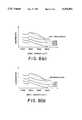
- FIG. 6(a)shows the change of the moisture content (wt %) in a film against an applied electric power under the conditions that the wafer temperature is at 400° C. and the plasma processing time is maintained constant at one minute, and also shows that the moisture content is reduced to about half as compared with a sample applied with no plasma processing.
- FIG. 8(b)shows the change of the moisture content (wt %) against the plasma processing time under the conditions that the wafer temperature is at 400° C. and the applied electric power is at 200 W, and also shows that the moisture content is reduced to about half as compared with a sample applied with no plasma processing.
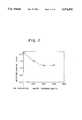
- FIG. 7shows the change of the moisture content (wt %) in a film against the wafer temperature under the conditions that the applied electric power is at 200 W and the plasma processing time is maintained constant at one minute, and also shows that the moisture content is reduced to about half as compared with a sample applied with no plasma processing.
- FIG. 8(a)shows the content of H 2 O with respect to the processed sample under the conditions that the plasma processing time is one minute and the wafer temperature is maintained constant at 400° C., and shows the change of absorbance with respect to the wave number (nm -1 ) with the applied electric power as a parameter.
- the absorbance shown along the ordinatesis assigned arbitrarlly with respect to respective lines corresponding to respective parameters.
- FIG. 8(b)shows the content of H 2 O for a sample processed with the plasma processing time as a parameter under the conditions that the applied electric power is at 200 W and the wafer temperature is maintained constant at 400° C.
- FIG. 9shows the content of H 2 O for a sample processed with the wafer temperature as a parameter under the conditions that the applied electric power is at 200 W and the plasma processing time is maintained constant at one minute.
- H 2 Odisappears by applying plasma processing, and the CVD SiO 2 film 11a becomes denser.
- Thisis considered to be caused by fact that H 2 O and the like are discharged from the CVD SiO 2 film 11 by active radical particles in the plasma colliding with the surface of the CVD SiO 2 film 11 or with the surface and the interior of the CVD SiO 2 film 11, which are irradiated with ultraviolet light generated by discharge.
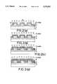
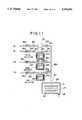
- FIGS. 1(a) to 1(d)show a series of sectional views explaining a first embodiment of a manufacturing method according to the present invention:
- FIGS. 2(a) to 2(d)show a series of sectional views explaining a second embodiment of a manufacturing method according to the present invention:
- FIGS. 3(a) and 3(b)show sectional views illustrating an experiment in a manufacturing method according to the present invention
- FIGS. 4a and 4bare graphs for the; results of investigation on the etching rate of a CVD SiO 2 film formed by a manufacturing method of the present invention.
- FIGS. 5(a) and 5(b)are graphs showing infrared absorption spectra of CVD SiO 2 films formed by the manufacturing method of the present invention.
- FIGS. 6(a) and 6(b)are graphs showing moisture content of a CVD SiO 2 film formed by the manufacturing method of the present invention.
- FIG. 7is a graph showing moisture content of a CVD SiO 2 film formed by a manufacturing method of the present invention.
- FIGS. 8(a) and 8(b)are graphs showing infrared absorption spectra of CVD SiO 2 films formed by a manufacturing method of the present invention.
- FIG. 9is a graph showing infrared absorption spectra of CVD SiO 2 films formed by a manufacturing method of the present invention.
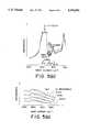
- FIGS. 10(a) and 10(b)are schematic diagrams showing a plasma processing system related to an embodiment of the present invention.
- FIG. 11is a schematic diagrams of a CVD film forming system related to an embodiment of the present invention.
- FIGS. 1(a) to (d)are sectional views explaining a method for forming an interlevel insulating film in the first and the second embodiments of the present invention.
- FIG. 11is a schematic diagram of a CVD system used for forming an interlevel insulating film
- FIGS. 10(a) and (b)are structural diagrams of a plasma processing system used for plasma processing of an interlevel insulating film formed by the CVD system shown in FIG. 11 according to an embodiment of the present invention.
- FIG. 11shows a CVD system for forming a SiO 2 film by a thermal CVD method a mixed gas of TEOS/O 3 .
- reference numeral 26represents a chamber
- 27represents a reaction gas inlet port for introducing reaction gas into the chamber
- 28represents an outlet port for reducing pressure in the chamber 26 and/or exhausting processed gas and the like out of the chamber
- 30represents a wafer placement table on which a wafer 1 is placed and containing a heater for heating the wafer 1
- 31represents a gas nozzle for directing the reaction gas onto the wafer 1.
- 32arepresents a gas pipe for feeding the reaction gas to the chamber 26, and gas pipings 32b, 32c, 32e and 32g for feeding ozone (O 3 ) gas, nitrogen gas containing a TEOS solution are connected thereto.
- 32brepresents a gas piping for feeding oxygen (O 2 ) gas or ozone gas generated by an ozonizer 33
- 32crepresents a gas piping for feeding nitrogen (N 2 ) gas containing a TEOS solution
- 32erepresents a gas piping for feeding nitrogen gas containing a TMPO or TMOP (Tri Methyl Phosphate: PO (OCH 3 ) 3 : hereinafter referred to as TMOP) solution
- 32grepresents a gas piping for feeding nitrogen gas containing TEB (Tri Ethyl Borote) solution.
- on/off valves 35a to 35c, 35e and 35gare provided on respective gas pipings 32b, 32c, 32e and 32g.
- 32d, 32f and 32hrepresent gas pipings for feeding nitrogen gas to the TEOS solution, the TMOP solution and the TEB solution, respectively, and on/off valves 35d, 35f and 35h are provided on respective gas pipings 32d, 32f and 32h.
- 33represents an ozonizer connected to the gas piping 32b
- 34a to 34crepresent heaters for heating and heat insulating the TEOS solution, and TMOP solution and the TEB solution, respectively
- 36a to 36drepresent mass flow controllers for regulating flow rate of oxygen gas and nitrogen gas as carrier gas.
- the TMOP solutionis used for forming a PSG (phosphorous glass) film
- the TEB solutionis used for forming a BSG (boron glass) film
- both of these solutionsare used for forming a BPSG (boron-phosphorous glass) film.
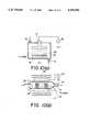
- FIG. 10(a)shows a plane parallel plate type plasma processing system.
- a reference numeral 12 in the figurerepresents a chamber
- 13represents a gas inlet port for introducing processing gas into the chamber 12
- 14represents an exhaust port for reducing pressure in the chamber 12 and/or exhausting spent gas and the like
- 16represents a wafer placement table containing internally a heater for heating the wafer 1
- 17represents one electrode for converting the gas into plasma. Alternating voltage is applied between this electrode 17 and the wafer placement table 16 connected to ground by means of an RF power supply 18 connected to the electrode 17 so that the processing gas introduced into the chamber 12 is converted into plasma.
- FIG. 10(b)shows another hot-wall type plasma processing system capable of batch processing.
- a reference numeral 19 in the figurerepresents a chamber composed of a quartz tube
- 20represents a gas inlet port for introducing processing gas into the chamber 19
- 21represents an exhaust port for reducing pressure in the chamber 19 and/or exhausting spent gas and the like
- 23represents a pair of discharge electrodes for converting the processing gas into plasma. Alternating voltage is applied between one electrode and the other electrode connected to ground by means of an RF power supply 24 connected to one electrode so that the processing gas introduced into the chamber 19 is converted into plasma.
- a SiO 2 film 2is formed on a Si substrate (wafer: semiconductor substrate) 1 by the thermal oxidization, and Al interconnections 3a to 3d are formed on the SiO 2 film 2 thereafter.
- valves 35a and 35bare opened so as to conduct oxygen gas into the ozonizer 33, thereby to introduce the oxygen gas into a gas piping 32 so as to obtain an ozone gas concentration in oxygen gas of approximately 1% with regulating by mass flow controller 36a.
- valves 35c and 35dare opened at the same time, and nitrogen gas at a predetermined flow rate, including the TEOS solution, is introduced to the gas piping 32, with regulating, by a mass flow controller 36b.
- the mixed gas of TEOS/O 3 introduced into the gas piping 32 as described abovepasses through the gas inlet port 27 of the chamber 26 and is introduced into the chamber 26.
- reactionoccurs on the wafer 1, and a CVD SiO 2 film 4 starts to form.
- This stateis maintained for a predetermined period of time, and Al interconnections 3a to 3c on the wafer 1 are covered by the CVD SiO 2 film 4 having a film thickness of approximately 8,000 ⁇ (FIG. 1 (b)) .
- the wafer 1is taken out of the chamber 26 of the CVD system, and placed on the wafer placement table 16 in the chamber 12 of the plane parallel plate type plasma processing system shown in FIG. 10(a) for the purpose of reforming the CVD SiO 2 film 4.
- the wafer temperatureis maintained at approximately 350° C. by the heater, and oxygen gas is introduced through a gas inlet port 13 while exhausting the inside of the chamber 12 through a gas exhaust port 14 and the inside of the chamber 12 is maintained at a predetermined pressure.
- high frequency voltage with a frequency of 13.56 MHzis applied between the electrode 17 and the wafer placing table 16 by the RF power supply 18 so as to convert the oxygen gas into plasma.
- the CVD SiO 2 film 4is held for 60 minutes while keeping it exposed to oxygen plasma gas, thus completely reforming of the CVD SiO 2 film 4 (FIGS. 1 (c) and (d)) .
- the CVD SiO 2 film 4is formed at a low temperature.
- a a CVD SiO 2 film 4 formed from a mixed gas of TEOS-O 3is used at the temperature of 400° C. in the first embodiment, but it may be formed within the range of 350° C. to 450° C. Further, a CVD SiO 2 film formed of silanc (SiH 4 )/oxygen (O 2 ) at temperature of from 350° C. to 450° C. may also be used.
- oxygen gasis used as the gas to be converted into plasma, but it is also possible to use inert gas such as nitrogen gas and argon gas.
- a CVD SiO 2 film (insultating film) 4 having a film thickness of approximately 8,000 ⁇is formed on the body using the CVD system shown in FIG. 11 similarly to the first embodiment.
- the wafer 1is taken out of the chamber 26 of the CVD system, and placed on the wafer, placement table 16 in the chamber 12 of the plane parallel plate type plasma processing system shown in FIG. 10(a) for the purpose of reforming the CVD SiO 2 film 4.
- the wafer 1is heated by the heater contained inside the wafer placement table 16 so as to maintain the wafer temperature at approximately 400° C.
- the inside of the chamber 12is exhausted through the exhaust port 14, and ammonia gas is introduced through the gas inlet port 13 when a predetermined pressure is reached so as to maintain the pressure inside the chamber 12 at approximately 1 Torr.
- the CVD SiO 2 film 4 thus formedwas investigated for:
- the moisture contentwas found to be reduced approximately half as compared with a case in which no processing is performed as shown in FIGS. 6(a), (b) and 7, and peaks showing existence of moisture (H 2 O) disappear as shown in FIGS. 8(a), (b) and 9. Accordingly, it is considered that the CVD SiO 2 film 11a has become denser.
- the CVD SiO 2 film 4was left in the atmosphere as is for one week, no change was shown in the moisture content of the CVD SiO 2 film 4. This fact shows that a primary factor causing generation of moisture has been removed from the inside of the CVD SiO 2 film 4a and migration of new moisture from the outside of the CVD SiO 2 film 4 is prevented, and that the CVD SiO 2 film 11a has been made denser.
- the CVD SiO 2 film 4is formed at a low temperature. Hence, it is possible to prevent hillocks and the like of Al interconnections 3a to 3c from forming.
- the wafer temperatureis set at 400° C. in plasma processing, but it may be set within the range of 200° C. to 400° C. Further, high frequency electric power for plasma conversion is set at 200 W, but power on the order of 100 to 300 W may be adopted.
- FIGS. 2(a) to (d)are sectional views for explaining a method for forming an interlevel insulating film in the third embodiment of a manufacturing method of the present invention. Plasma processing using oxygen gas is performed.
- a predetermined film thickness of 8,000 ⁇is finally formed by applying the manufacturing method of the present invention to thickness of 2,000 ⁇ instead of forming the film with a predetermined film thickness of 8,000 ⁇ .
- Al interconnections 3a to 3care formed after forming a SiO 2 film 2 on a Si substrate (wafer: semiconductor substrate) 1 by thermal oxidation.
- a first CVD SiO 2 film 5 having a film thickness of approximately 2,000 ⁇is formed similarly to the first embodiment from a mixed gas of TEOS/O 3 using the CVD system shown in FIG. 11.
- the first CVD SiO 2 film 5is exposed to oxygen gas converted into plasma for about 30 minutes at approximately 400° C. using the plasma processing system shown in FIG. 10(a).
- the film thickness of the first CVD SiO 2 film 5is sufficiently thin as shown in FIGS. 4(a), (b) and 5(a), (b) (hereinafter referred to as FIG. 4(a) and others), the film quality is improved extending over the entire film thickness.
- a second CVD SiO 2 film 6 having film thickness of approximately 2,000 ⁇is formed similarly to the process shown in FIG. 2(a), and plasma processing is applied by oxygen gas converted into plasma (FIG. 2(b)).
- plasma processingis applied by oxygen gas converted into plasma (FIG. 2(b)).
- the film thickness of the second CVD SiO 2 film 6is also sufficiently thin, the film quality is improved extending over the entire film thickness as shown in FIG. 4(a) and others.
- a third CVD SiO 2 film 7 having a film thickness of approximately 2,000 ⁇is formed and applied with plasma processing similarly to the above (FIG. 2(c)).
- a fourth CVD SiO 2 film 8is formed and applied with plasma processing (FIG. 2(d)).
- the film qualityis improved extending over the entire film thickness as shown in FIG. 4(a) and others.
- a predetermined film thickness of 8,000 ⁇is finally formed by applying the manufacturing method of the present invention to each successive sufficiently thin film having a thickness of 2,000 ⁇ . Therefore, it is possible to further improve the film quality of the CVD SiO 2 films 5 to 8 as compared with the first embodiment.
- FIGS. 2(a) to (d)are sectional views explaining a method for forming an interlevel insulating film in the fourth embodiment of a manufacturing method of the present invention. Plasma processing using ammonia gas is performed therein.
- a predetermined film thickness of 8,000 ⁇is finally formed by applying the manufacturing method of the present invention to each of plural films, each having a thickness of 2,000 ⁇ , instead of forming the predetermined film thickness of 8,000 ⁇ at once.
- Al interconnections 3a to 3care formed similarly to the second embodiment.
- a first CVD SiO 2 film (insulating film) 5 having a film thickness of approximately 2,000 ⁇is formed similarly to the second embodiment from a mixed gas of TEOS/O 3 using the CVD system shown in FIG. 11.
- the first CVD SiO 2 film 5is exposed to ammonia gas converted into plasma for about one minute with the wafer temperature at approximately 400° C. using the plasma processing system shown in FIG. 10(a).
- the film thickness of the first CVD SiO 2 film 5is sufficiently thin, the film quality is improved extending over the entire film thickness as shown in FIGS. 6(a), (b). 7, 8(c), (b) and 9 (hereinafter referred to as FIG. 6(a) and others).
- a second CVD SiO 2 film (insulating film) 6 having a film thickness of approximately 2,000 ⁇is formed similarly to the process shown in FIG. 2(a), and exposed to ammonia gas converted into plasma (FIG. 2(b)).
- the film qualityis improved extending over the entire film thickness since the film thickness of the second CVD SiO 2 film 6 is also sufficiently thin.
- a third CVD SiO 2 film (insulating film) 7 having a film thickness of approximately 2,000 ⁇is formed and applied with plasma processing (FIG. 2(c)) similarly to the above.
- a fourth CVD SiO 2 film (insulating film) 8is formed and applied with plasma processing (FIG. 2(d)).
- the film qualityis improved extending over the entire film thickness since the film thicknesses of both the third and the fourth CVD SiO 2 films 7 and 8 are sufficiently thin.
- a predetermined film thickness of 8,000 ⁇is finally formed by applying the manufacturing method of the present invention to plural successive sufficiently thin films of thickness of 2,000 ⁇ .
- the film quality of the CVD SiO 2 films 5 to 8can be further improved as a whole as compared with the first embodiment.
Landscapes
- Engineering & Computer Science (AREA)
- Physics & Mathematics (AREA)
- Condensed Matter Physics & Semiconductors (AREA)
- General Physics & Mathematics (AREA)
- Manufacturing & Machinery (AREA)
- Computer Hardware Design (AREA)
- Microelectronics & Electronic Packaging (AREA)
- Power Engineering (AREA)
- Plasma & Fusion (AREA)
- Chemical & Material Sciences (AREA)
- Chemical Kinetics & Catalysis (AREA)
- Formation Of Insulating Films (AREA)
Abstract
Description
Claims (18)
Priority Applications (2)
| Application Number | Priority Date | Filing Date | Title |
|---|---|---|---|
| EP92109549AEP0572704B1 (en) | 1992-06-05 | 1992-06-05 | Method for manufacturing a semiconductor device including method of reforming an insulating film formed by low temperature CVD |
| US07/895,472US5376591A (en) | 1992-06-05 | 1992-06-08 | Method for manufacturing semiconductor device |
Applications Claiming Priority (2)
| Application Number | Priority Date | Filing Date | Title |
|---|---|---|---|
| EP92109549AEP0572704B1 (en) | 1992-06-05 | 1992-06-05 | Method for manufacturing a semiconductor device including method of reforming an insulating film formed by low temperature CVD |
| US07/895,472US5376591A (en) | 1992-06-05 | 1992-06-08 | Method for manufacturing semiconductor device |
Publications (1)
| Publication Number | Publication Date |
|---|---|
| US5376591Atrue US5376591A (en) | 1994-12-27 |
Family
ID=26130947
Family Applications (1)
| Application Number | Title | Priority Date | Filing Date |
|---|---|---|---|
| US07/895,472Expired - Fee RelatedUS5376591A (en) | 1992-06-05 | 1992-06-08 | Method for manufacturing semiconductor device |
Country Status (2)
| Country | Link |
|---|---|
| US (1) | US5376591A (en) |
| EP (1) | EP0572704B1 (en) |
Cited By (26)
| Publication number | Priority date | Publication date | Assignee | Title |
|---|---|---|---|---|
| US5532193A (en)* | 1993-11-10 | 1996-07-02 | Canon Sales Co., Inc. | Method for forming insulating film |
| US5652187A (en)* | 1991-10-30 | 1997-07-29 | Samsung Electronics Co., Ltd. | Method for fabricating doped interlayer-dielectric film of semiconductor device using a plasma treatment |
| US5656556A (en)* | 1996-07-22 | 1997-08-12 | Vanguard International Semiconductor | Method for fabricating planarized borophosphosilicate glass films having low anneal temperatures |
| US5716890A (en)* | 1996-10-18 | 1998-02-10 | Vanguard International Semiconductor Corporation | Structure and method for fabricating an interlayer insulating film |
| US5814558A (en)* | 1994-08-31 | 1998-09-29 | Texas Instruments Incorporated | Interconnect capacitance between metal leads |
| US5818111A (en)* | 1997-03-21 | 1998-10-06 | Texas Instruments Incorporated | Low capacitance interconnect structures in integrated circuits using a stack of low dielectric materials |
| US5976900A (en)* | 1997-12-08 | 1999-11-02 | Cypress Semiconductor Corp. | Method of reducing impurity contamination in semiconductor process chambers |
| US6054769A (en)* | 1997-01-17 | 2000-04-25 | Texas Instruments Incorporated | Low capacitance interconnect structures in integrated circuits having an adhesion and protective overlayer for low dielectric materials |
| US6146928A (en)* | 1996-06-06 | 2000-11-14 | Seiko Epson Corporation | Method for manufacturing thin film transistor, liquid crystal display and electronic device both produced by the method |
| US6225236B1 (en)* | 1998-02-12 | 2001-05-01 | Canon Sales Co., Inc. | Method for reforming undercoating surface and method for production of semiconductor device |
| US6287989B1 (en)* | 1992-07-04 | 2001-09-11 | Trikon Technologies Limited | Method of treating a semiconductor wafer in a chamber using hydrogen peroxide and silicon containing gas or vapor |
| US6383951B1 (en)* | 1998-09-03 | 2002-05-07 | Micron Technology, Inc. | Low dielectric constant material for integrated circuit fabrication |
| US6429147B2 (en)* | 1997-06-30 | 2002-08-06 | Sony Corporation | Method for making an insulating film |
| US6440860B1 (en) | 2000-01-18 | 2002-08-27 | Micron Technology, Inc. | Semiconductor processing methods of transferring patterns from patterned photoresists to materials, and structures comprising silicon nitride |
| US6461950B2 (en) | 1998-09-03 | 2002-10-08 | Micron Technology, Inc. | Semiconductor processing methods, semiconductor circuitry, and gate stacks |
| US6511923B1 (en)* | 2000-05-19 | 2003-01-28 | Applied Materials, Inc. | Deposition of stable dielectric films |
| US6514884B2 (en) | 1998-02-06 | 2003-02-04 | Semiconductor Process Laboratory Co., Ltd. | Method for reforming base surface, method for manufacturing semiconductor device and equipment for manufacturing the same |
| US20030113480A1 (en)* | 2001-12-10 | 2003-06-19 | Hynix Semiconductor Inc. | Method for forming high dielectric layers using atomic layer deposition |
| US6727173B2 (en) | 1998-09-03 | 2004-04-27 | Micron Technology, Inc. | Semiconductor processing methods of forming an utilizing antireflective material layers, and methods of forming transistor gate stacks |
| US6828683B2 (en) | 1998-12-23 | 2004-12-07 | Micron Technology, Inc. | Semiconductor devices, and semiconductor processing methods |
| US20050003655A1 (en)* | 1998-02-27 | 2005-01-06 | Micron Technology, Inc. | MOCVD process using ozone as a reactant to deposit a metal oxide barrier layer |
| US6878507B2 (en) | 1998-02-25 | 2005-04-12 | Micron Technology, Inc. | Semiconductor processing methods |
| US7067415B2 (en) | 1999-09-01 | 2006-06-27 | Micron Technology, Inc. | Low k interlevel dielectric layer fabrication methods |
| US7235499B1 (en) | 1999-01-20 | 2007-06-26 | Micron Technology, Inc. | Semiconductor processing methods |
| US7804115B2 (en) | 1998-02-25 | 2010-09-28 | Micron Technology, Inc. | Semiconductor constructions having antireflective portions |
| US20140065808A1 (en)* | 2012-08-31 | 2014-03-06 | Globalfoundries Inc. | Method of forming a material layer in a semiconductor structure |
Families Citing this family (4)
| Publication number | Priority date | Publication date | Assignee | Title |
|---|---|---|---|---|
| JPH0817174B2 (en)* | 1993-11-10 | 1996-02-21 | キヤノン販売株式会社 | Method of modifying insulating film |
| JP3061255B2 (en)* | 1995-08-18 | 2000-07-10 | キヤノン販売株式会社 | Film formation method |
| US6015759A (en)* | 1997-12-08 | 2000-01-18 | Quester Technology, Inc. | Surface modification of semiconductors using electromagnetic radiation |
| GB9801655D0 (en)* | 1998-01-28 | 1998-03-25 | Trikon Equip Ltd | Method and apparatus for treating a substrate |
Citations (17)
| Publication number | Priority date | Publication date | Assignee | Title |
|---|---|---|---|---|
| US3850687A (en)* | 1971-05-26 | 1974-11-26 | Rca Corp | Method of densifying silicate glasses |
| JPS5522862A (en)* | 1978-08-07 | 1980-02-18 | Nec Corp | Manufacturing method for silicon oxidized film |
| JPS55113335A (en)* | 1979-02-23 | 1980-09-01 | Fujitsu Ltd | Manufacture of semiconductor device |
| GB2086871A (en)* | 1980-10-24 | 1982-05-19 | Suwa Seikosha Kk | A method of chemical vapour deposition |
| US4361461A (en)* | 1981-03-13 | 1982-11-30 | Bell Telephone Laboratories, Incorporated | Hydrogen etching of semiconductors and oxides |
| JPS6046036A (en)* | 1983-08-23 | 1985-03-12 | Nec Corp | Manufacture of semiconductor device |
| US4590091A (en)* | 1984-12-17 | 1986-05-20 | Hughes Aircraft Company | Photochemical process for substrate surface preparation |
| US4708884A (en)* | 1984-07-11 | 1987-11-24 | American Telephone And Telegraph Company, At&T Bell Laboratories | Low temperature deposition of silicon oxides for device fabrication |
| JPS6425543A (en)* | 1987-07-22 | 1989-01-27 | Hitachi Ltd | Manufacture of film including silicon oxide |
| US4845054A (en)* | 1985-06-14 | 1989-07-04 | Focus Semiconductor Systems, Inc. | Low temperature chemical vapor deposition of silicon dioxide films |
| US4872947A (en)* | 1986-12-19 | 1989-10-10 | Applied Materials, Inc. | CVD of silicon oxide using TEOS decomposition and in-situ planarization process |
| JPH0219232A (en)* | 1988-06-24 | 1990-01-23 | Tokyo Autom Mach Works Ltd | Size altering mechanism of carton feed apparatus |
| US4985372A (en)* | 1989-02-17 | 1991-01-15 | Tokyo Electron Limited | Method of forming conductive layer including removal of native oxide |
| EP0421203A1 (en)* | 1989-09-28 | 1991-04-10 | Applied Materials, Inc. | An integrated circuit structure with a boron phosphorus silicate glass composite layer on semiconductor wafer and improved method for forming same |
| US5013691A (en)* | 1989-07-31 | 1991-05-07 | At&T Bell Laboratories | Anisotropic deposition of silicon dioxide |
| EP0436185A1 (en)* | 1989-12-27 | 1991-07-10 | Semiconductor Process Laboratory Co., Ltd. | Process for forming SiO2 film with polysiloxane/ozone reaction |
| US5166101A (en)* | 1989-09-28 | 1992-11-24 | Applied Materials, Inc. | Method for forming a boron phosphorus silicate glass composite layer on a semiconductor wafer |
Family Cites Families (2)
| Publication number | Priority date | Publication date | Assignee | Title |
|---|---|---|---|---|
| DE2058059A1 (en)* | 1969-11-26 | 1971-06-09 | Hitachi Ltd | Circuit device having a compacted coating film on a substrate and method for its manufacture |
| DD97673A1 (en)* | 1972-08-01 | 1973-05-14 |
- 1992
- 1992-06-05EPEP92109549Apatent/EP0572704B1/ennot_activeExpired - Lifetime
- 1992-06-08USUS07/895,472patent/US5376591A/ennot_activeExpired - Fee Related
Patent Citations (17)
| Publication number | Priority date | Publication date | Assignee | Title |
|---|---|---|---|---|
| US3850687A (en)* | 1971-05-26 | 1974-11-26 | Rca Corp | Method of densifying silicate glasses |
| JPS5522862A (en)* | 1978-08-07 | 1980-02-18 | Nec Corp | Manufacturing method for silicon oxidized film |
| JPS55113335A (en)* | 1979-02-23 | 1980-09-01 | Fujitsu Ltd | Manufacture of semiconductor device |
| GB2086871A (en)* | 1980-10-24 | 1982-05-19 | Suwa Seikosha Kk | A method of chemical vapour deposition |
| US4361461A (en)* | 1981-03-13 | 1982-11-30 | Bell Telephone Laboratories, Incorporated | Hydrogen etching of semiconductors and oxides |
| JPS6046036A (en)* | 1983-08-23 | 1985-03-12 | Nec Corp | Manufacture of semiconductor device |
| US4708884A (en)* | 1984-07-11 | 1987-11-24 | American Telephone And Telegraph Company, At&T Bell Laboratories | Low temperature deposition of silicon oxides for device fabrication |
| US4590091A (en)* | 1984-12-17 | 1986-05-20 | Hughes Aircraft Company | Photochemical process for substrate surface preparation |
| US4845054A (en)* | 1985-06-14 | 1989-07-04 | Focus Semiconductor Systems, Inc. | Low temperature chemical vapor deposition of silicon dioxide films |
| US4872947A (en)* | 1986-12-19 | 1989-10-10 | Applied Materials, Inc. | CVD of silicon oxide using TEOS decomposition and in-situ planarization process |
| JPS6425543A (en)* | 1987-07-22 | 1989-01-27 | Hitachi Ltd | Manufacture of film including silicon oxide |
| JPH0219232A (en)* | 1988-06-24 | 1990-01-23 | Tokyo Autom Mach Works Ltd | Size altering mechanism of carton feed apparatus |
| US4985372A (en)* | 1989-02-17 | 1991-01-15 | Tokyo Electron Limited | Method of forming conductive layer including removal of native oxide |
| US5013691A (en)* | 1989-07-31 | 1991-05-07 | At&T Bell Laboratories | Anisotropic deposition of silicon dioxide |
| EP0421203A1 (en)* | 1989-09-28 | 1991-04-10 | Applied Materials, Inc. | An integrated circuit structure with a boron phosphorus silicate glass composite layer on semiconductor wafer and improved method for forming same |
| US5166101A (en)* | 1989-09-28 | 1992-11-24 | Applied Materials, Inc. | Method for forming a boron phosphorus silicate glass composite layer on a semiconductor wafer |
| EP0436185A1 (en)* | 1989-12-27 | 1991-07-10 | Semiconductor Process Laboratory Co., Ltd. | Process for forming SiO2 film with polysiloxane/ozone reaction |
Non-Patent Citations (10)
| Title |
|---|
| Electronics Letters, vol. 26, No. 11, May 24, 1990, Enage GB pp. 733 734, XP000108687, K. Aite et al. Novel Low Temperature RF Plasma Annealing using NH3 N2 Gas Mixture .* |
| Electronics Letters, vol. 26, No. 11, May 24, 1990, Enage GB pp. 733-734, XP000108687, K. Aite et al. "Novel Low Temperature RF Plasma Annealing using NH3-N2 Gas Mixture". |
| Fujino et al "Surface Modification of Base Material for TEOS/Oo3 . . ." J. of Electromechanical Soc. vol. 139, No. 6 (Jun. 1992). |
| Fujino et al Surface Modification of Base Material for TEOS/Oo 3 . . . J. of Electromechanical Soc. vol. 139, No. 6 (Jun. 1992).* |
| J. Vac. Sci Technol B3(5) Sep./Oct. 1985 pp. 1352 1356.* |
| J. Vac. Sci Technol B3(5) Sep./Oct. 1985 pp. 1352-1356. |
| RCA Review, vol. 37, No. 1, Mar. 1976, Princeton US pp. 55 77 W. Kern Densification of Vapor Deposited Phosphosilicate Glass Films . pp. 55, paragraph 1 p. 56, paragraph 2; FIG. 3.* |
| RCA Review, vol. 37, No. 1, Mar. 1976, Princeton US pp. 55-77 W. Kern "Densification of Vapor-Deposited Phosphosilicate Glass Films". pp. 55, paragraph 1-p. 56, paragraph 2; FIG. 3. |
| Wolf, Silicon Processing for the VLSI Era vol. 1 Process Tech. pp. 182 189 & 504.* |
| Wolf, Silicon Processing for the VLSI Era vol. 1 Process Tech. pp. 182-189 & 504. |
Cited By (43)
| Publication number | Priority date | Publication date | Assignee | Title |
|---|---|---|---|---|
| US5652187A (en)* | 1991-10-30 | 1997-07-29 | Samsung Electronics Co., Ltd. | Method for fabricating doped interlayer-dielectric film of semiconductor device using a plasma treatment |
| US6287989B1 (en)* | 1992-07-04 | 2001-09-11 | Trikon Technologies Limited | Method of treating a semiconductor wafer in a chamber using hydrogen peroxide and silicon containing gas or vapor |
| US5532193A (en)* | 1993-11-10 | 1996-07-02 | Canon Sales Co., Inc. | Method for forming insulating film |
| US5814558A (en)* | 1994-08-31 | 1998-09-29 | Texas Instruments Incorporated | Interconnect capacitance between metal leads |
| US6146928A (en)* | 1996-06-06 | 2000-11-14 | Seiko Epson Corporation | Method for manufacturing thin film transistor, liquid crystal display and electronic device both produced by the method |
| US5656556A (en)* | 1996-07-22 | 1997-08-12 | Vanguard International Semiconductor | Method for fabricating planarized borophosphosilicate glass films having low anneal temperatures |
| US5716890A (en)* | 1996-10-18 | 1998-02-10 | Vanguard International Semiconductor Corporation | Structure and method for fabricating an interlayer insulating film |
| US6054769A (en)* | 1997-01-17 | 2000-04-25 | Texas Instruments Incorporated | Low capacitance interconnect structures in integrated circuits having an adhesion and protective overlayer for low dielectric materials |
| US5818111A (en)* | 1997-03-21 | 1998-10-06 | Texas Instruments Incorporated | Low capacitance interconnect structures in integrated circuits using a stack of low dielectric materials |
| US6429147B2 (en)* | 1997-06-30 | 2002-08-06 | Sony Corporation | Method for making an insulating film |
| US5976900A (en)* | 1997-12-08 | 1999-11-02 | Cypress Semiconductor Corp. | Method of reducing impurity contamination in semiconductor process chambers |
| US6514884B2 (en) | 1998-02-06 | 2003-02-04 | Semiconductor Process Laboratory Co., Ltd. | Method for reforming base surface, method for manufacturing semiconductor device and equipment for manufacturing the same |
| US6225236B1 (en)* | 1998-02-12 | 2001-05-01 | Canon Sales Co., Inc. | Method for reforming undercoating surface and method for production of semiconductor device |
| US7825443B2 (en) | 1998-02-25 | 2010-11-02 | Micron Technology, Inc. | Semiconductor constructions |
| US7626238B2 (en) | 1998-02-25 | 2009-12-01 | Micron Technology, Inc. | Semiconductor devices having antireflective material |
| US6878507B2 (en) | 1998-02-25 | 2005-04-12 | Micron Technology, Inc. | Semiconductor processing methods |
| US7804115B2 (en) | 1998-02-25 | 2010-09-28 | Micron Technology, Inc. | Semiconductor constructions having antireflective portions |
| US20050003655A1 (en)* | 1998-02-27 | 2005-01-06 | Micron Technology, Inc. | MOCVD process using ozone as a reactant to deposit a metal oxide barrier layer |
| US6835995B2 (en) | 1998-09-03 | 2004-12-28 | Micron Technology, Inc. | Low dielectric constant material for integrated circuit fabrication |
| US6727173B2 (en) | 1998-09-03 | 2004-04-27 | Micron Technology, Inc. | Semiconductor processing methods of forming an utilizing antireflective material layers, and methods of forming transistor gate stacks |
| US6383951B1 (en)* | 1998-09-03 | 2002-05-07 | Micron Technology, Inc. | Low dielectric constant material for integrated circuit fabrication |
| US6461950B2 (en) | 1998-09-03 | 2002-10-08 | Micron Technology, Inc. | Semiconductor processing methods, semiconductor circuitry, and gate stacks |
| US7576400B1 (en) | 1998-09-03 | 2009-08-18 | Micron Technology, Inc. | Circuitry and gate stacks |
| US7151054B2 (en) | 1998-09-03 | 2006-12-19 | Micron Technology, Inc. | Semiconductor processing methods of forming and utilizing antireflective material layers, and methods of forming transistor gate stacks |
| US6828683B2 (en) | 1998-12-23 | 2004-12-07 | Micron Technology, Inc. | Semiconductor devices, and semiconductor processing methods |
| US7279118B2 (en) | 1998-12-23 | 2007-10-09 | Micron Technology, Inc. | Compositions of matter and barrier layer compositions |
| US7235499B1 (en) | 1999-01-20 | 2007-06-26 | Micron Technology, Inc. | Semiconductor processing methods |
| US7521354B2 (en) | 1999-09-01 | 2009-04-21 | Micron Technology, Inc. | Low k interlevel dielectric layer fabrication methods |
| US7067415B2 (en) | 1999-09-01 | 2006-06-27 | Micron Technology, Inc. | Low k interlevel dielectric layer fabrication methods |
| US7067414B1 (en) | 1999-09-01 | 2006-06-27 | Micron Technology, Inc. | Low k interlevel dielectric layer fabrication methods |
| US7078356B2 (en) | 1999-09-01 | 2006-07-18 | Micron Technology, Inc. | Low K interlevel dielectric layer fabrication methods |
| US7045277B2 (en) | 2000-01-18 | 2006-05-16 | Micron Technology, Inc. | Semiconductor processing methods of transferring patterns from patterned photoresists to materials, and structures comprising silicon nitride |
| US7208805B2 (en) | 2000-01-18 | 2007-04-24 | Micron Technology, Inc. | Structures comprising a layer free of nitrogen between silicon nitride and photoresist |
| US7078328B2 (en) | 2000-01-18 | 2006-07-18 | Micron Technology, Inc. | Semiconductor processing methods of transferring patterns from patterned photoresists to materials, and structures comprising silicon nitride |
| US7435688B2 (en) | 2000-01-18 | 2008-10-14 | Micron Technology, Inc. | Semiconductor processing methods of transferring patterns from patterned photoresists to materials, and structures comprising silicon nitride |
| US6858523B2 (en) | 2000-01-18 | 2005-02-22 | Micron Technology, Inc. | Semiconductor processing methods of transferring patterns from patterned photoresists to materials, and structures comprising silicon nitride |
| US7638436B2 (en) | 2000-01-18 | 2009-12-29 | Micron Technology, Inc. | Semiconductor processing methods of transferring patterns from patterned photoresists to materials |
| US6440860B1 (en) | 2000-01-18 | 2002-08-27 | Micron Technology, Inc. | Semiconductor processing methods of transferring patterns from patterned photoresists to materials, and structures comprising silicon nitride |
| US6511923B1 (en)* | 2000-05-19 | 2003-01-28 | Applied Materials, Inc. | Deposition of stable dielectric films |
| US6849300B2 (en) | 2001-12-10 | 2005-02-01 | Hynix Semiconductor, Inc. | Method for forming high dielectric layers using atomic layer deposition |
| US20030113480A1 (en)* | 2001-12-10 | 2003-06-19 | Hynix Semiconductor Inc. | Method for forming high dielectric layers using atomic layer deposition |
| US20140065808A1 (en)* | 2012-08-31 | 2014-03-06 | Globalfoundries Inc. | Method of forming a material layer in a semiconductor structure |
| US8993459B2 (en)* | 2012-08-31 | 2015-03-31 | Globalfoundries Inc. | Method of forming a material layer in a semiconductor structure |
Also Published As
| Publication number | Publication date |
|---|---|
| EP0572704A1 (en) | 1993-12-08 |
| EP0572704B1 (en) | 2000-04-19 |
Similar Documents
| Publication | Publication Date | Title |
|---|---|---|
| US5376591A (en) | Method for manufacturing semiconductor device | |
| EP0015694B1 (en) | Method for forming an insulating film on a semiconductor substrate surface | |
| US5387546A (en) | Method for manufacturing a semiconductor device | |
| US5800877A (en) | Method for forming a fluorine containing silicon oxide film | |
| KR100292456B1 (en) | Method and apparatus for forming germanium doped BPSG thin film | |
| US6297175B1 (en) | Method for improving thickness uniformity of deposited ozone-TEOS silicate glass layers | |
| KR100300177B1 (en) | Method and apparatus for improving film stability of halogen-doped silicon oxide films | |
| US20030143410A1 (en) | Method for reduction of contaminants in amorphous-silicon film | |
| EP0573911A2 (en) | Method for depositing silicon oxide films of improved properties | |
| JPH04360533A (en) | Chemical vapor deposition method | |
| JP6058876B2 (en) | Method for depositing SiO2 film | |
| KR20130014543A (en) | Conformal layers by radical-component cvd | |
| JP2015521375A (en) | Improved densification for flowable membranes | |
| JP4044637B2 (en) | A method for improving the interface quality of plasma-excited CVD films. | |
| JPH05267480A (en) | Semiconductor device and its manufacture | |
| KR100391485B1 (en) | Manufacturing method and apparatus of device using ferroelectric film | |
| JPH0766186A (en) | Anisotropic depositing method of dielectric | |
| EP0481706B1 (en) | Method of producing CVD silicon oxynitride film | |
| JPH04233734A (en) | Fluorization silicon nitride adhesion method | |
| JPH06168937A (en) | Manufacture of silicon oxide film | |
| US6090725A (en) | Method for preventing bubble defects in BPSG film | |
| JP2588446B2 (en) | Semiconductor device | |
| JP2004103688A (en) | Method for forming insulating film and gate insulating film | |
| JPH0574763A (en) | Method for forming gate insulating film | |
| JP2742381B2 (en) | Method of forming insulating film |
Legal Events
| Date | Code | Title | Description |
|---|---|---|---|
| AS | Assignment | Owner name:SEMICONDUCTOR PROCESS LABORATORY CO., LTD., A JAPA Free format text:ASSIGNMENT OF ASSIGNORS INTEREST.;ASSIGNORS:MAEDA, KAZUO;TOKUMASU, NOBORU;NISHIMOTO, YUKO;REEL/FRAME:006229/0862 Effective date:19920525 Owner name:CANON SALES CO., INC., A JAPANESE CORP., JAPAN Free format text:ASSIGNMENT OF ASSIGNORS INTEREST.;ASSIGNORS:MAEDA, KAZUO;TOKUMASU, NOBORU;NISHIMOTO, YUKO;REEL/FRAME:006229/0862 Effective date:19920525 Owner name:ALCAN-TECH CO., INC., A JAPANESE CORP., JAPAN Free format text:ASSIGNMENT OF ASSIGNORS INTEREST.;ASSIGNORS:MAEDA, KAZUO;TOKUMASU, NOBORU;NISHIMOTO, YUKO;REEL/FRAME:006229/0862 Effective date:19920525 | |
| CC | Certificate of correction | ||
| FEPP | Fee payment procedure | Free format text:PAYOR NUMBER ASSIGNED (ORIGINAL EVENT CODE: ASPN); ENTITY STATUS OF PATENT OWNER: LARGE ENTITY | |
| FPAY | Fee payment | Year of fee payment:4 | |
| FPAY | Fee payment | Year of fee payment:8 | |
| FEPP | Fee payment procedure | Free format text:PAYER NUMBER DE-ASSIGNED (ORIGINAL EVENT CODE: RMPN); ENTITY STATUS OF PATENT OWNER: LARGE ENTITY Free format text:PAYOR NUMBER ASSIGNED (ORIGINAL EVENT CODE: ASPN); ENTITY STATUS OF PATENT OWNER: LARGE ENTITY | |
| REMI | Maintenance fee reminder mailed | ||
| LAPS | Lapse for failure to pay maintenance fees | ||
| STCH | Information on status: patent discontinuation | Free format text:PATENT EXPIRED DUE TO NONPAYMENT OF MAINTENANCE FEES UNDER 37 CFR 1.362 | |
| FP | Lapsed due to failure to pay maintenance fee | Effective date:20061227 |