US5376580A - Wafer bonding of light emitting diode layers - Google Patents
Wafer bonding of light emitting diode layersDownload PDFInfo
- Publication number
- US5376580A US5376580AUS08/036,532US3653293AUS5376580AUS 5376580 AUS5376580 AUS 5376580AUS 3653293 AUS3653293 AUS 3653293AUS 5376580 AUS5376580 AUS 5376580A
- Authority
- US
- United States
- Prior art keywords
- led
- substrate
- layers
- wafer bonding
- layer
- Prior art date
- Legal status (The legal status is an assumption and is not a legal conclusion. Google has not performed a legal analysis and makes no representation as to the accuracy of the status listed.)
- Expired - Lifetime
Links
Images


Classifications
- H—ELECTRICITY
- H10—SEMICONDUCTOR DEVICES; ELECTRIC SOLID-STATE DEVICES NOT OTHERWISE PROVIDED FOR
- H10H—INORGANIC LIGHT-EMITTING SEMICONDUCTOR DEVICES HAVING POTENTIAL BARRIERS
- H10H20/00—Individual inorganic light-emitting semiconductor devices having potential barriers, e.g. light-emitting diodes [LED]
- H10H20/01—Manufacture or treatment
- H—ELECTRICITY
- H01—ELECTRIC ELEMENTS
- H01L—SEMICONDUCTOR DEVICES NOT COVERED BY CLASS H10
- H01L25/00—Assemblies consisting of a plurality of semiconductor or other solid state devices
- H01L25/03—Assemblies consisting of a plurality of semiconductor or other solid state devices all the devices being of a type provided for in a single subclass of subclasses H10B, H10D, H10F, H10H, H10K or H10N, e.g. assemblies of rectifier diodes
- H01L25/04—Assemblies consisting of a plurality of semiconductor or other solid state devices all the devices being of a type provided for in a single subclass of subclasses H10B, H10D, H10F, H10H, H10K or H10N, e.g. assemblies of rectifier diodes the devices not having separate containers
- H01L25/075—Assemblies consisting of a plurality of semiconductor or other solid state devices all the devices being of a type provided for in a single subclass of subclasses H10B, H10D, H10F, H10H, H10K or H10N, e.g. assemblies of rectifier diodes the devices not having separate containers the devices being of a type provided for in group H10H20/00
- H01L25/0756—Stacked arrangements of devices
- H—ELECTRICITY
- H10—SEMICONDUCTOR DEVICES; ELECTRIC SOLID-STATE DEVICES NOT OTHERWISE PROVIDED FOR
- H10H—INORGANIC LIGHT-EMITTING SEMICONDUCTOR DEVICES HAVING POTENTIAL BARRIERS
- H10H20/00—Individual inorganic light-emitting semiconductor devices having potential barriers, e.g. light-emitting diodes [LED]
- H10H20/01—Manufacture or treatment
- H10H20/011—Manufacture or treatment of bodies, e.g. forming semiconductor layers
- H10H20/012—Manufacture or treatment of bodies, e.g. forming semiconductor layers having light-emitting regions comprising only Group II-IV materials
- H10H20/0125—Manufacture or treatment of bodies, e.g. forming semiconductor layers having light-emitting regions comprising only Group II-IV materials with a substrate not being Group II-VI materials
- H—ELECTRICITY
- H10—SEMICONDUCTOR DEVICES; ELECTRIC SOLID-STATE DEVICES NOT OTHERWISE PROVIDED FOR
- H10H—INORGANIC LIGHT-EMITTING SEMICONDUCTOR DEVICES HAVING POTENTIAL BARRIERS
- H10H20/00—Individual inorganic light-emitting semiconductor devices having potential barriers, e.g. light-emitting diodes [LED]
- H10H20/01—Manufacture or treatment
- H10H20/011—Manufacture or treatment of bodies, e.g. forming semiconductor layers
- H10H20/013—Manufacture or treatment of bodies, e.g. forming semiconductor layers having light-emitting regions comprising only Group III-V materials
- H—ELECTRICITY
- H10—SEMICONDUCTOR DEVICES; ELECTRIC SOLID-STATE DEVICES NOT OTHERWISE PROVIDED FOR
- H10H—INORGANIC LIGHT-EMITTING SEMICONDUCTOR DEVICES HAVING POTENTIAL BARRIERS
- H10H20/00—Individual inorganic light-emitting semiconductor devices having potential barriers, e.g. light-emitting diodes [LED]
- H10H20/01—Manufacture or treatment
- H10H20/011—Manufacture or treatment of bodies, e.g. forming semiconductor layers
- H10H20/018—Bonding of wafers
- H—ELECTRICITY
- H10—SEMICONDUCTOR DEVICES; ELECTRIC SOLID-STATE DEVICES NOT OTHERWISE PROVIDED FOR
- H10H—INORGANIC LIGHT-EMITTING SEMICONDUCTOR DEVICES HAVING POTENTIAL BARRIERS
- H10H20/00—Individual inorganic light-emitting semiconductor devices having potential barriers, e.g. light-emitting diodes [LED]
- H10H20/80—Constructional details
- H10H20/81—Bodies
- H10H20/8215—Bodies characterised by crystalline imperfections, e.g. dislocations; characterised by the distribution of dopants, e.g. delta-doping
- H—ELECTRICITY
- H10—SEMICONDUCTOR DEVICES; ELECTRIC SOLID-STATE DEVICES NOT OTHERWISE PROVIDED FOR
- H10H—INORGANIC LIGHT-EMITTING SEMICONDUCTOR DEVICES HAVING POTENTIAL BARRIERS
- H10H20/00—Individual inorganic light-emitting semiconductor devices having potential barriers, e.g. light-emitting diodes [LED]
- H10H20/80—Constructional details
- H10H20/81—Bodies
- H10H20/822—Materials of the light-emitting regions
- H10H20/824—Materials of the light-emitting regions comprising only Group III-V materials, e.g. GaP
- H—ELECTRICITY
- H01—ELECTRIC ELEMENTS
- H01L—SEMICONDUCTOR DEVICES NOT COVERED BY CLASS H10
- H01L2924/00—Indexing scheme for arrangements or methods for connecting or disconnecting semiconductor or solid-state bodies as covered by H01L24/00
- H01L2924/0001—Technical content checked by a classifier
- H01L2924/0002—Not covered by any one of groups H01L24/00, H01L24/00 and H01L2224/00
- H—ELECTRICITY
- H10—SEMICONDUCTOR DEVICES; ELECTRIC SOLID-STATE DEVICES NOT OTHERWISE PROVIDED FOR
- H10H—INORGANIC LIGHT-EMITTING SEMICONDUCTOR DEVICES HAVING POTENTIAL BARRIERS
- H10H20/00—Individual inorganic light-emitting semiconductor devices having potential barriers, e.g. light-emitting diodes [LED]
- H10H20/80—Constructional details
- H10H20/81—Bodies
- H10H20/816—Bodies having carrier transport control structures, e.g. highly-doped semiconductor layers or current-blocking structures
- H10H20/8162—Current-blocking structures
Definitions
- the present inventionrelates generally to light emitting diodes and more particularly to methods of fabricating light emitting diodes.
- LEDsLight emitting diodes
- LEDsare employed in a wide variety of applications. For example, in optical data transmission, LEDs are used to launch data signals along a fiberoptic cable.
- LEDsdo not generate well-focused beams of light. Rather, an LED radiates light in all directions. That is, the light emission is isotropic.
- the layers of many conventional LEDsare grown on an optically absorbing substrate having an energy gap less than the emission energy of the active region of the LED. The substrate absorbs some of the light generated within the active region, thereby reducing the efficiency of the device.
- AlGaAsaluminum gallium arsenide
- An epitaxial layer 10 of p-doped AlGaAs and an epitaxial layer 12 of n-doped AlGaAsare grown on a surface of a p-doped gallium arsenide (GaAs) substrate 14.
- GaAsgallium arsenide
- FIG. 2is a double heterojunction AlGaAs LED on an absorbing substrate 16.
- An epitaxial layer 18 of n-doped AlGaAs and two layers 20 and 22 of p-doped AlGaAsare grown on the absorbing substrate 16.
- the bandgaps of the epitaxial layers 18-22are chosen to cause light to be generated in the active layer 20 and to travel through the epitaxial layers 18 and 22 without being absorbed. However, absorption of light does occur at the substrate 16.
- Improved performancecan be achieved by employing a transparent substrate that has an energy gap greater than the emission energy of the LED active region.
- the effect of the transparent substrateis to prevent the downwardly emitted or directed light from being absorbed. Rather, the light passes through the transparent substrate and is reflected from a bottom metal adhesive and reflecting cup. The reflected light is then emitted from the top or the edges of the chip to substantially improve the efficiency of the LED.
- a first techniqueis to epitaxially grow the p-n junction on a transparent substrate.
- a problem with this techniqueis that acceptable lattice matching may be difficult to achieve, depending upon the lattice constant of the LED epitaxial layers.
- a second techniqueis to grow the LED epitaxial layers on an absorbing substrate that is later removed. For example, in FIG. 3 the n-doped transparent substrate 24 and the p-doped epitaxial layers 26 and 28 may be epitaxially grown on an absorbing substrate, not shown.
- the transparent "substrate” 24is fabricated by growing a thick, greater than 75 ⁇ m, optically transparent and electrically conductive epitaxial layer on the lattice-matched absorbing substrate. The other layers 26 and 28 are then grown on the epitaxial "substrate” 24 and the absorbing substrate is removed. Alternatively, the thinner layers 26 and 28 may be grown before the thicker transparent "substrate” 24.
- an absorbing substrate or a transparent substratemay possess mechanical characteristics that are superior to a transparent substrate LED, but the absorbing substrate LED is generally less efficient. Increased efficiency is possible using a transparent substrate; however, lattice mismatch may create difficulties when the epitaxial layers are grown on a transparent substrate having a different lattice constant. In addition, the contradictory thickness problems may be encountered when a "thick" transparent "substrate” is epitaxially grown.
- the effect of an absorbing layer or substratecan be minimized by growing a Bragg reflector between the standard LED epitaxial layers and the absorbing substrate.
- An increase in efficiencyis achieved, since the Bragg reflector will reflect light that is emitted or internally reflected in the direction of the absorbing substrate.
- the improvementis limited compared to transparent substrate techniques, because the Bragg reflector only reflects light that is of near normal incidence. Light that differs from a normal incidence by a significant amount is not reflected and passes to the substrate, where it is absorbed.
- LEDs having Bragg reflectorsare more difficult to manufacture, since they require the repeated growth of many thin epitaxial layers, typically on the order of 100 angstroms in thickness.
- the above objecthas been met by a method that utilizes a temporary growth substrate optimized for the growth of LED layers, but then provides a performance-enhancing substrate without requiring the epitaxial growth of this substrate.
- the performance-enhancing substrateis a transparent member that is joined to the LED layers using wafer bonding techniques. Because the transparent layer is not bonded to the LED layers until completion of epitaxial growth of the LED layers, lattice matching of the transparent substrate and epitaxial layers is not a concern.
- the temporary growth substrateis made of a material compatible with fabricating LED layers having desired mechanical characteristics. For example, in order to achieve high crystal quality growth and to optimize lattice matching, standard absorbing substrate materials may be utilized. LED layers are then grown using one or more of a variety of methods, including liquid phase epitaxy, vapor phase epitaxy, metalorganic chemical vapor deposition and/or molecular beam epitaxy.
- the LED layers that form an LED structuremay consist of a light-emitting active layer, upper and lower confining layers, current spreading and light extraction layers and one or more buffer layers, but this is not critical.
- the temporary absorbing growth substratehas completed its purpose of allowing the formation of high-quality epitaxial layers.
- the growth substrateis preferably removed, since the absorbing growth substrate has an energy gap that is less than or equal to the emission energy of the LED structure. Such a relationship between the energy gap and the emission energy of the device would significantly limit the efficiency of the device.
- the method of removing the temporary growth substrateis not critical, alternatives include chemical etching, lapping/polishing, reactive ion etching, and ion milling. Removing the growth substrate may further include removal of a portion or all of the layer that contacts the absorbing substrate.
- a second substrateis then wafer bonded to the LED structure.
- the second waferis electrically conductive and is optically transparent.
- the transparent substrateis a performance-enhancing layer. Wafer bonding can occur at the uppermost or lowermost layer of the LED structure.
- the LED deviceincludes electrodes at opposed ends for properly biasing the p-n junction of the device, so that minimizing the resistivity at the interface of the transparent substrate and the grown layers is important. Utilizing compounds that include indium has been shown to aid in achieving desired ohmic characteristics.
- In-bearing compoundsIn addition to In-bearing compounds, other compounds with a high surface mobility, high diffusivity, and/or superior mass transport properties (e.g., Hg-bearing, Cd-bearing and Zn-bearing compounds) may provide advantages when used in solid-state wafer bonding applications.
- Hg-bearing, Cd-bearing and Zn-bearing compoundsmay provide advantages when used in solid-state wafer bonding applications.
- the temporary growth substrateis removed only after attachment of the second substrate to the uppermost layer of the LED structure. Utilizing wafer bonding of the second substrate, rather than epitaxially growing the second substrate, permits attachment of a thick substrate, e.g. 8 mils or more.
- This second substratemay be transparent and act as a performance-enhancing layer for optical extraction and current spreading and/or act only as a means for obtaining improved mechanical stability during the steps of removing the growth substrate and performing a second wafer bonding of a transparent substrate at the side of the LED structure from which the growth substrate was removed. If only mechanical stability is desired, this second substrate may be subsequently removed after the second wafer bonding step is performed.
- the temporary growth substratemay be a transparent substrate having a low electrical conductivity that limits its current spreading ability. Such a substrate would ultimately limit the efficiency of the LED. Thus, removal of the temporary transparent growth substrate for replacement by a transparent substrate having a higher electrical conductivity would improve the performance of the device. Similarly, one absorbing layer having a low electrical conductivity may be replaced with an absorbing layer having a higher electrical conductivity.
- a "wafer bond layer”is defined herein as a layer or substrate that exhibits the properties that are characteristic of a layer that has undergone wafer bonding. It is believed that one such characteristic is a different nature of misfit dislocations formed at the wafer bonded interface, compared to an epitaxially grown mismatched heterointerface. An interface that has undergone wafer bonding has been observed to exhibit misfit dislocations which primarily consist of "edge dislocations,” i.e. dislocations whose Burgers vector lies in the plane of the wafer bonded interface.
- layersare epitaxially grown on a first growth substrate that is not necessarily removed at a later time.
- Many Al-bearing III-V semiconductorsare unstable in moist ambients and will undergo degradation by hydrolysis. Such degradation may cause reliability problems for LEDs containing Al-bearing III-V epitaxial layers of significant thickness.
- an AlGaAs LEDsuch as the one shown in FIG. 3 will undergo significant degradation as a result of oxidation of the high Al-composition layer 28 during wet high-temperature reliability testing. This degradation may potentially be reduced by employing wafer bonding.
- the majority of the thickness of the high Al-composition layer 28may be replaced by a thick optically transparent, electrically conductive wafer-bond layer which does not contain a high composition of Al.
- a wafer-bond layer of GaPmay be substituted for a major portion of the transparent substrate 24. That is, it is possible to employ the wafer bonding technique to achieve passivation.
- an electrically conductive mirrorcan be wafer bonded to the LED layers that form the LED structure. Light emitted in the direction of the mirror is then reflected back to the LED structure so as to improve the efficiency of the device.
- the mirroris typically supported by a substrate, which may be an absorbing substrate or a transparent substrate, since light does not reach the substrate itself.
- Wafer bondingcan also be used to provide increased mechanical and/or thermal stability, regardless of any optical benefits.
- a robust III-V semiconductor wafer or a SiC wafercan be bonded to a II-VI LED structure to add stability.
- At least one of the wafer surfaces to be wafer bondedis patterned in a manner to selectively vary the electrical and/or optical properties of the wafer. For example, depressions may be formed at selected areas prior to wafer bonding to define desired current paths to the active region of the LED. Possible applications include, but are not limited to, reducing light directed at metallized electrodes for applying voltages to LEDs and simplifying the fabrication of spot emitters. Patterning may also be used to vary optical properties along the wafer surface, so as to redirect light in a desired manner.
- the wafer-bond interfaceis preferably one having a low electrical resistivity and good mechanical strength. It has been discovered that van der Waals' forces are typically ineffective in obtaining the desired ohmic characteristics and structural integrity. It has also been discovered that a combination of pressure and high temperature processing more reliably achieves the desired ohmic and mechanical characteristics. In addition, the application of pressure at high temperatures allows the wafers to conform to each other, minimizing any problems which may result from unevenness of the wafer surfaces, especially for bonding relatively thick layers.
- An advantage of the present inventionis that the performance of the resulting LED is enhanced. Both light extraction and current spreading can be improved. Another advantage is that a thick substrate of 8 mils or more can be formed in a cost efficient manner, since wafer bonding is not subjected to the limitations of epitaxially growing a substrate. The thick substrate provides improved handling and device mounting characteristics.
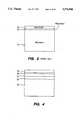
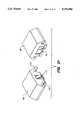
- FIG. 1is a side view of a prior art, single heterojunction LED device having an absorbing substrate.
- FIG. 2is a side view of a prior art, double heterojunction LED device having an absorbing substrate.
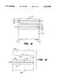
- FIG. 3is a side view of a prior art, double heterojunction LED device having a transparent substrate.
- FIG. 4is a side view of a double heterojunction LED device having a temporary growth substrate in accordance with the present invention.
- FIG. 5is a side view of an LED structure having the growth substrate of FIG. 4 removed.
- FIG. 6is a side view of the LED structure of FIG. 5 having a permanent substrate attached using wafer bonding techniques.
- FIG. 7is a side view of the structure of FIG. 6 having electrodes on opposed sides.
- FIG. 8is a side view of an alternative LED structure fabricated by wafer bonding.
- FIG. 9is a side view of a third embodiment of attaching a wafer-bond substrate to the device of FIG. 4.
- FIG. 10is a side view of another embodiment of attaching a wafer-bond substrate to the LED structure of FIG. 5.
- FIG. 11is a side view of the LED structure of FIG. 5 attached to a mirror by the use of wafer bonding techniques.
- FIG. 12is a side view of a stacked LED device.
- FIGS. 13-17are side views of LED devices utilizing patterned layers that are wafer bonded.
- FIG. 18is an exploded view of a wafer bonding apparatus for carrying out the steps of the present invention.
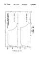
- FIG. 19is a graph of temperature profiles for operating the apparatus of FIG. 18.
- FIG. 20is a schematic view of an alternate apparatus for carrying out the steps of the present invention.
- FIGS. 21 and 22are different embodiments of graphite members for use with the apparatus of FIG. 20.
- a first step in carrying out the inventionis to select a substrate 30 onto which a plurality of LED layers will be sequentially grown.
- the substrate 30is a temporary growth substrate which is removed subsequent to fabrication of the LED layers.
- the electrical and optical properties of the substrateare irrelevant to the operation of the LED to be fabricated, so that the substrate can be selected solely for properties which affect the growth of the LED layers. For example, lattice matching is typically an important consideration in the selection of the substrate. However, in some embodiments the substrate may remain, so that properties other than growth-compatibility are important to these embodiments.
- An exemplary temporary growth substrate 30is a GaAs substrate within the range of 250 to 500 ⁇ m thick.
- Four LED layers 32, 34, 36 and 38are then grown on the growth substrate 30.
- the layers 32-38may be grown using any of a variety of known methods, including liquid phase epitaxy, vapor phase epitaxy, metalorganic chemical vapor deposition and molecular beam epitaxy.
- the layers 32-38form a double heterojunction LED, but the invention may be utilized with any type of LED device.
- the layer 32 directly above the growth substrate 30is an n-doped buffer layer.
- a lower confining layer of n-doped AlGaInPis grown above the buffer layer.
- the lower confining layer 34has an exemplary thickness of 800 nanometers.
- An active layer 36 of AlGaInPis grown to an exemplary thickness of 500 nanometers.
- An upper confining layer 38 of p-doped AlGaInPthen completes the structure of FIG. 4.
- the upper confining layerhas an exemplary thickness of 800 nanometers.
- a window layerthat is transparent and that has a higher electrical conductivity than the layers 34, 36 and 38 may be grown atop the upper confining layer 38 in order to promote current spreading, thereby enhancing the performance of the resulting structure.
- Such a window layeris described in U.S. Pat. No. 5,008,718 to Fletcher et al.
- the growth substratehas been removed, leaving the LED structure formed by the grown layers 32-38. Removal of the growth substrate can be accomplished in various ways, including chemical etching, lapping/polishing, reactive ion etching, ion milling, or any combination thereof. As will be described more fully below, the method of removing the substrate is not critical so long as a clean, planar surface is presented following the removal.
- the buffer layer 32may be wholly or partially removed and the lower confining layer may be partially removed.
- a performance-enhancing substrateis bonded to either the lowermost layer 32 or the uppermost layer 38 of the LED structure 40 shown in FIG. 5.
- the location of the wafer to be bondeddepends upon the LED structure 40 and the electrical and optical properties of the grown layers 32-38 and/or the substrate to be bonded.
- a wafer bonding techniqueis employed. Wafer bonding offers a number of advantages over other methods of providing a performance-enhancing substrate to an LED.
- FIG. 6illustrates an embodiment in which an electrically conductive, optically transparent substrate 42 has been wafer bonded to the buffer layer 32.
- the wafer bondingoffers the advantage that a transparent substrate may be provided without requiring the growth of such a substrate.
- the wafer bonded transparent substrate 42has a thickness exceeding 8 mils.
- Growing a substrate having a comparable thicknesswould be difficult or impossible utilizing conventional techniques, and would require an extremely long time. Because only the relatively thin layers 32-38 of the LED structure 40 need to be grown, epitaxial growth times can be drastically reduced, thereby maximizing throughput.
- the wafer bonding processprovides a thick device having enhanced mechanical properties, as compared to transparent substrates which are epitaxially grown.
- Wafer bondingmay also be utilized to displace the p-n junction from the bottom of the device, so as to reduce the possibility of short-circuiting the device when it is mounted in conductive silver-loaded epoxy, as is conventional in the art.
- An electrode 44is formed on the upper confining layer 38, as for example by evaporation.
- a typical material for forming the electrodeis a gold-zinc alloy.
- a second electrode 46is formed on the transparent substrate 42. Again, evaporation may be used, but this is not critical.
- a typical materialis gold-germanium alloy.
- a second substrate 48has been wafer bonded to the structure of FIG. 4. That is, a second substrate is wafer bonded before removal of the temporary growth substrate 30.
- the second substrate 48is a "thick" layer exceeding 6 mils. Wafer bonding prior to removal of the growth substrate 30 would significantly improve the mechanical stability of the device, since there would be no time in which the epitaxial layers 32-38 would be unsupported by a substrate.
- a buffer layermay be epitaxially grown on the second substrate 48 prior to wafer bonding. Such an epitaxial buffer layer may also be utilized with a substrate that replaces the growth substrate 30 at the bottom of the buffer layer 32.
- the device of FIG. 4may be a conventional structure having the layers 32-38 grown on a transparent or absorbing substrate 30.
- the wafer bond layer 48 of FIG. 8would then be a thick, electrically conductive, optically transparent layer, such as the current-spreading window layer described above with reference to U.S. Pat No. 5,008,718 to Fletcher et al.
- the top layer 48it is also possible to remove the original growth substrate 30 and wafer bond another performance-enhancing substrate to the bottom of the remaining structure for reasons of improving optical extraction and/or current spreading.
- the device of FIG. 4may have a conventional transparent layer 30 that possesses a low electrical conductivity, limiting the current spreading ability of the device.
- the increase in electrical conductivitywould improve the performance of the device.
- the substitute transparent substrateshould be wafer bonded to the exposed LED layers with low electrical conductivity.
- the substitute transparent substrate having the higher electrical conductivitycould be wafer bonded to the LED structure either before or after removal of the transparent layer with low electrical conductivity.
- temporary growth absorbing substratesmay be replaced with absorbing substrates having a higher electrical conductivity. While the use of wafer bonding to attach an absorbing layer is not the preferred embodiment, such wafer bonding would indeed improve the performance of the LED device.
- wafer bondingmay also be employed in providing passivation to the structures of either FIG. 4 or FIG. 6.
- Many Al-bearing III-V semiconductorsare unstable in moist ambients, since such semiconductors are susceptible to degradation by hydrolysis.
- the degradationmay cause reliability problems in LEDs containing Al-bearing III-V epitaxial layers 30-38 of significant thickness.
- degradationmay result from oxidation of the high Al-bearing confining layer 38 during wet, high-temperature use.
- the degradationcan be retarded if the majority of the Al-bearing layer is replaced by a thick optically transparent, electrically conductive wafer bond layer that does not contain a high Al composition.
- the wafer-bond layer 50may be GaP.
- the desired electrical connection between the transparent substrate 42 and the LED structure 40can be ensured by utilizing a metallization scheme.
- thin contact areascan be formed on the upper surface of the substrate 42 to be wafer bonded.
- Corresponding contact areascan be formed on the lowermost layer 32 of the LED structure. Contacts having a thickness of less than 1000 angstroms are preferred. While the pattern of contacts should be sufficiently great to ensure the proper electrical contact, the total area covered by the contact should be sufficiently small that the interface between the LED structure and the substrate 42 allows the passage of light to and from the transparent substrate. The contacts may or may not be alloyed.
- the surface of the substrateis then brought into contact with the surface of the lowermost layer 32 and the device is annealed at elevated temperatures. The anneal achieves a wafer bond in the non-metallized areas and provides a bond at the metallized contacts.
- a layer 52 of glass or SiO 2 or other oxidecan be formed on an optically transparent, electrically conductive substrate 54. The layer 52 is then patterned to provide areas for contact metallization 56, as in the embodiment described immediately above.
- an oxide and/or contact metallization 58may be patterned on the lowermost layer 32 of the LED structure 40. Again, the contacts should be patterned to provide a sufficient area for good electrical contact, while occupying a total area that still renders the interface largely optically transparent.
- the surface of the layer 52is then brought into contact with the surface of the buffer layer 32, and treatment forms a wafer bond between the layers. Annealing will enhance the bonding strength between the materials.
- the LED structure 40 described abovemay be wafer bonded to a mirror 60.
- the mirror 60will then reflect any downwardly emitted or previously reflected internal light. The reflection will increase the light output of the device.
- the mirror 60is supported by a substrate 62.
- the optical properties of the substrateare not relevant, since light is reflected before reaching the substrate.
- the mirror 60 and the substrate 62should be made of electrically conductive material, allowing an electrode to be coupled to the substrate for biasing the LED structure 40.
- the mirrormay also consist of an epitaxially grown or a deposited Bragg reflector. Materials such as silicon, GaAs or even some metals may be employed to form the substrate 62. These materials may provide further improvement of the device, if the device is operated at high temperatures or high currents, since some of these materials, e.g. Si, have a relatively high thermal conductivity.
- Stacked LED devicesmay also be formed using the wafer bonding process. Such a device is shown in FIG. 12. Multiple LED structures 40 and 64 may be bonded together and/or bonded to other layers if the interfaces are such that a high electrical conductivity is maintained through the device.
- the doping type of the layers 34 and 38 of the upper LED structure 40corresponds to the doping type of the layers 70 and 66, respectively, of the lower LED structure 64.
- the two LED structures 40 and 64are arranged with the same polarity.
- the surfaces to be wafer bondedshould be prepared such that they are very heavily doped.
- a heavily doped tunnel junction 72having the opposite polarity of the LED structures is formed.
- the tunnel junctionmay be epitaxially grown as part of one of the LED structures with wafer bonding occurring to the exposed surface of this junction.
- the device of FIG. 12is operated by applying a voltage at an upper electrode 74 and a voltage at lower electrodes 76 such that the individual LED structures 40 and 64 are forward biased.
- the lower electrodesare a patterned metallization on an electrically conductive, optically transparent substrate 78.
- the forward biasing of the stacked devicereverse biases the heavily doped tunnel junction 72, causing the tunnel junction to conduct. In this manner, an arbitrary number of LEDs can be stacked together for improved light output and efficiency.
- the LED device comprised of the stack of LED structures 40 and 64would operate at the summation of the voltages of the individual LED structures, if the LED structures were not stacked together. It is not critical that the active layers 36 and 68 possess the same emission energy. However, the substrate 78 preferably has an energy gap greater than the emission energies of the individual LED structures. It should be noted that the stack may also be formed if all of the conductivity types are inverted.
- the wafer-bond layeris a semiconductor having a thickness that exceeds 1 mil.
- Acceptable materialsinclude Si, Ge, AlP, AlSb, GaN, AlN, GaP, GaAs, GaSb, InP, InAs, InSb, ZnS, ZnSe, CdSe, CdTe, SiC, or any combination of alloys of the above.
- the wafer-bond substratemay be commercially available or may consist of epitaxially grown layers added to a commercially available substrate. The epitaxially grown layers are added for reasons such as increasing the bonding strength of the substrate or the electrical conductivity of the wafer-bond interface.
- the wafer-bond substrateis solely a thick, i.e., greater than 1 mil, epitaxial layer of the above-listed materials which has been removed from a temporary growth substrate. It is further possible that the wafer bond layer be a thinner, e.g. 2 ⁇ m, epitaxial layer formed on a temporary growth substrate. Such a layer is then wafer bonded and this growth substrate subsequently removed.
- FIG. 13illustrates an embodiment in which a patterned semiconductor wafer 126 is wafer bonded to an LED structure 128 comprising an upper confining layer 130, an active layer 132 and a lower confining layer 134.
- the LED structuremay be grown onto a substrate 136, or may be wafer bonded to the substrate 136.
- the patterned semiconductor wafer 126may be a current-spreading window layer such as the one described with reference to FIG. 8, but this is not critical.
- the patterned wafer 126is etched at a lower surface 138 to form a depression 140. The presence of the depression will cause variations in both the electrical and optical properties when the patterned wafer is joined to the LED structure.
- the patterned semiconductor wafer 126has been wafer bonded to the upper confining layer 130 of the LED structure 128. Electrodes 142 and 144 are then formed on the upper surface of the patterned wafer 126 and the lower surface of the substrate 136. The depression 140 in the patterned wafer creates a cavity, or void. The application of a voltage at the electrode 142 will cause the conduction of current to the LED structure 128, but no current will flow to the region directly beneath the cavity, as shown by the current flow arrows in FIG. 14.
- Electrode regionsare typically absorbing regions. Consequently, restricting current flow in the manner illustrated in FIG. 14 will improve the efficiency of the LED device and provide an uncomplicated method of selecting electrical current flow paths.
- FIG. 15shows a spot emitter 142 that includes an LED structure 144 on a substrate 146. Depressions 148 and 150 are formed in a wafer-bond layer 152. The cavities at the interface of the LED structure and the wafer-bond layer function to define current flow from electrodes 154 and 156 to the interface. The defined flow path provides a current-injection region between the depressions 148 and 150, since the depressions limit the area of electrical contact at the interface. Current injection and light output at a central region are desirable in such applications as coupling the spot emitter 142 to a fiber optic device. In the preferred embodiment, the depressions 148 and 150 are different portions of a single annular cavity in which the inside diameter defines the central current-injection region.
- Patterning a semiconductor wafer which is to be wafer bondedmay also be employed advantageously to strategically redirect light that has been emitted from LED layers.
- the redirection of lightwill depend upon the device geometry, application and mounting.
- An exampleis shown in FIG. 16.
- LED layers 156are sandwiched between an upper layer 158 and a lower layer 160.
- Exterior layers 162 and 164are wafer bonded at opposed sides.
- Non-bonded regions 166, 168 and 170are formed sufficiently far from electrodes 172 to allow current to spread around the non-bonded regions. However, the cavities are sufficiently close to the electrodes to redirect light that would otherwise be absorbed by the electrodes. Thus, an increase in light extraction can be realized.
- the conduction of current from the electrode 172 to the LED layers 156is substantially unaffected by the non-bonded regions 166, 168 and 170, but light directed from the LED layers is affected.
- the redirection of lightoccurs as a result of a difference in the index of refraction between the non-bonded regions 166-170 and the adjacent layer.
- the index of refraction of the surrounding semiconductormay be approximately 3, whereas in the cavity it is approximately 1.
- the exact index of refraction at the non-bonded regionsdepends upon the semiconductor wafer bonding method. Typically, the bonding occurs in a gaseous environment, such as in H 2 or PH 3 . Thus, a cavity would tend to fill with the gas. Such gases have an index of refraction that is very close to 1 at standard pressure and temperature.
- the index of refraction of the semiconductorideally is greater than that of the cavity so that light does not tend to become trapped within the cavity, but this is not critical.
- a patterned LED layer 174includes depressions 176.
- a patterned layer 174may have been originally epitaxially grown or may have been wafer bonded onto underlying LED layers 178 on a substrate 180.
- a second substrate 182is wafer bonded to the upper surface of the patterned LED layer.
- the LED layer 174 and/or the substrate 182may be patterned.
- the depression 140may be formed in the semiconductor wafer 126 by standard etching techniques.
- Other methods that are well known in the artmay also be employed in patterning the surfaces of wafers to be bonded.
- other methodswould include selective diffusion or ion implantation to form reverse biased buried p-n junctions, the growth or deposition of insulating oxide layers in selective patterns, and any combination of the various available methods.
- oxide layersthe index of refraction of most oxides is approximately 1.6, which provides a sufficient index to redirect light in a means similar to the above-described cavities that are formed by etching and wafer bonding.
- Wafer bonding a patterned layerhas been tested using n-GaP substrates.
- a patterned n-GaP substratewas bonded to an unpatterned n-GaP substrate using techniques to be described below.
- the patterned substratewas formed by etching circular depressions having a diameter of approximately 175 ⁇ m and a depth of approximately 15 ⁇ m. The depressions were spaced apart by approximately 125 ⁇ m. For these dimensions, substrate patterning was easily achieved and the bond had sufficient mechanical strength to allow the substrates to be cleaved. Depressions with smaller dimensions, approximately 40 ⁇ m, have also been demonstrated. Extensions to dimensions of less than 10 ⁇ m should also be possible, permitting fine scale current definition and light scattering abilities.
- GaP-GaP bonds and InGaP-GaP bonds for either n-type or p-type unipolar bondshave been achieved using the techniques to be described, so that patterned wafers should be capable of conducting current across bonded regions while preventing current flow across non-bonded cavities.
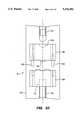
- FIG. 18illustrates a known device for achieving a wafer bond of a pair of wafers 80.
- the pair of wafersis placed face-to-face in a recessed area 82 within a first graphite member 84.
- the recessed area 82is a 0.5 inch by 0.8 inch area in the first graphite member.
- a second graphite member 86includes holes 88 positioned to receive alignment pins 90 projecting from the first graphite member.
- Graphite shimsmay be placed within the recessed area 82 to compensate for run-to-run variations in the thickness of the pair of wafers 80 to be bonded together.
- the assemblyis inserted inside a close-fitting quartz tube 92, which is then loaded into an open-tube furnace.
- the temperatureis raised to 850°-1000° C. in an H 2 ambient at a flow rate of 1.0 liter/min.
- the temperature cycleconsists of a ramp to the desired temperature, followed by a five second to one hour anneal. A cooling period then follows.
- the pair of wafers 80is compressed.
- the compressional forceis developed by the difference in the coefficients of thermal expansion of the quartz tube 92 (5.5 ⁇ 10 -7 /°C.) and the graphite members 84 and 86 (8.4 ⁇ 10 -6 /°C.).
- the coefficient of thermal expansion of the wafers 80e.g., 5.8 ⁇ 10 -6 /°C. for GaP
- III-V semiconductor wafersbecome somewhat plastic. Consequently, the wafer surfaces tend to conform to each other when compressed, helping to compensate for any unevenness of the wafer surfaces.
- the wafers 80Prior to loading in the wafer bonding apparatus of FIG. 18, the wafers 80 must be cleaned to remove any contamination or any oxides from the wafer surfaces. Organic contamination is typically removed by degreasing techniques. For the materials In x Ga 1-x P and GaP, the oxides are typically removed by etching in NH 4 OH. After etching, the wafers are immediately placed in methanol to remove any remaining NH 4 OH from the wafers. The surfaces to be bonded are placed into contact while the samples are still in the methanol.
- the contacting wafers 80are then removed from the methanol.
- the methanolquickly evaporates, leaving the wafers 80 bonded by van der Waals' forces.
- the van der Waals' bonddoes not generally provide sufficient mechanical strength and does not generally provide sufficient electrical conductivity to be employed in LED device fabrication as described above. Thus, further solid-state bonding is required.
- the wafer bonding apparatus of FIG. 18is therefore employed.
- the wafersconsisted of GaP:S (n ⁇ 5 ⁇ 10 17 cm -3 ) substrates [(100)+2° toward (110), or (100)+10° toward (110)] and of GaP:Zn (p ⁇ 2 ⁇ 10 18 cm -3 ) "pseudo-substrates" (prepared from ⁇ 2 mil-thick vapor phase epitaxy GaP grown on GaAs).
- GaAs substrateswere oriented (100)+2° toward (110). After solid-state wafer bonding, thermal damage from the exposed surfaces was generally removed by etching in HCl:HNO 3 :H 2 O (1:1:1). The wafers were then metallized with AuGe for n-type contacts and/or AuZn for p-type contacts, alloyed, and diced into chips.
- the preferred stepsinclude preparing the wafers with an NH 4 OH etch, followed by bringing the surfaces to be bonded into contact with each other while the wafers 80 are in a solution of methanol. Wafers that were bonded subsequent to a preparation that included these two steps were compared to wafers that were bonded after the alternative preparation process of an HF:deionized water (1:10) etch, followed by rinsing in deionized water and drying with N 2 .
- the bonded wafersconsisted of an n-type GaP substrate and n-type In 0 .5 Ga 0 .5 P (on GaAs:Te).
- the waferswere placed in the wafer bonding apparatus of FIG. 18.
- the waferswere identically annealed at 1000° C. for one hour.
- the current-voltage characteristicsclearly showed a relatively low resistance ohmic bond for the wafers prepared with NH 4 OH-methanol.
- the wafers prepared by etching in HF:deionized watershowed non-ohmic characteristics, as if a "barrier" were presented at the interface of the bonded wafer.
- Such non-ohmic characteristicsare generally intolerable for applications in which current is to be passed from one wafer-bonded substrate to another wafer-bonded substrate.
- the NH 4 OH-methanol surface preparationis presently considered to be the preferred preparation for achieving desired ohmic electrical characteristics when bonding n-type InGaP to n-type GaP.
- Other surface preparationssuch as NH 4 OH etching, rinsing in methanol and then drying with N 2 prior to contact result in non-ohmic characteristics.
- the same preparation when applied to bonding n-type In 0 .5 Ga 0 .5 P (on n-type GaAs:Te) to n-type In 0 .5 Ga 0 .5 P (GaAs:Te)resulted in the desired ohmic bonding characteristics.
- the differencesmay result from the inability of the surface preparation to remove all of the oxide from the GaP, whereas it is sufficient for the In 0 .5 Ga 0 .5 P.
- Another possible explanation for the differencesis that improved bonding properties have been exhibited for In-bearing compounds.
- the (a) unipolar n-type In 0 .5 Ga 0 .5 P/In 0 .5 Ga 0 .5 P bondexhibited a significantly lower resistance at the interface as compared to the (b) unipolar n-type In 0 .5 Ga 0 .5 P/GaP bond.
- the resistancewas approximately 1.5 ohms, while for (b) the resistance was approximately 5 ohms (20 ⁇ 20 mil die).
- the lower resistance In 0 .5 Ga 0 .5 P/In 0 .5 Ga 0 .5 P bondwas capable of being formed over the entire wafer area at a lower temperature of approximately 975° C., as compared to the In 0 .5 Ga 0 .5 P/GaP bond achieved at 1000° C.
- In-bearing compoundsare desirable for solid-state wafer bonding in use with LED fabrication.
- materialmay be transferred via shear stress, evaporation-condensation, and mass transport.
- the enhanced bonding observed with In-bearing compoundsmay be desirable as a result of a higher surface mobility of In atoms compared with Ga atoms or from improved mass-transport properties of In 0 .5 Ga 0 .5 P compared to GaP.
- Inis known to exhibit a relatively high diffusivity in AlGaAs-GaAs-InGaAs structures.
- the Inmay diffuse or alloy into the GaP during the solid-state wafer bonding process, forming an In x Ga 1-x P (x ⁇ 0.5) alloy around the bonded interface.
- III-V or II-VI compoundswith similar characteristics, i.e., a high atomic surface mobility and/or improved mass-transport properties, may also be advantageously employed for solid-state wafer bonding.
- Hg-bearing, Cd-bearing and Zn-bearing compoundsare prime candidates for such applications.
- FIG. 19shows two different profiles. In the upper profile a "fast" ramp to a temperature of 1000° C. was provided, while in the lower profile a “slow” ramp to 1000° C. was provided. In both cases, an anneal of one hour followed the ramp to 1000° C. Identical cooling profiles are shown.
- the lower, "slow” rampgenerally resulted in ohmic bonding at lower temperatures and over substantially larger areas. This phenomena may result from the bonded surfaces not being in compression during some portion of the high temperature ramp. This would allow some degree of surface decomposition or thermal oxide desorption prior to wafer bonding. Also, such differences could result from a longer effective anneal provided by the "slow” ramp. However, the effect was only observed in bonding n-type to n-type wafers. No such dependency was observed in bonding p-type to p-type wafers.
- Wafer bonding of p-GaP to p-GaP and also of n-GaP to n-GaPwas performed. In both cases, the bonding was performed at 1000° C. for one hour. Ohmic bonding occurred over the entire sample areas for both n-type and p-type bonding. However, the bonding resistance was significantly lower for the GaP/GaP p-type unipolar wafer bonds (less than 0.9 ohm) than the GaP/GaP n-type unipolar wafer bonds (approximately 5 ohms) for 12 ⁇ 12 mil chips. The relative ease of forming ohmic bonds between p-type samples may be a result of the higher diffusion rate of p-type dopants compared to n-type dopants.
- a marked improvement in light output of approximately a factor of twowas achieved by removing the absorbing GaAs substrate and solid-state wafer bonding a transparent GaP substrate to an In 0 .5 (Al x Ga 1-x ) 0 .5 P LED, as compared to the same LED structure with the original growth absorbing GaAs substrate remaining.
- FIG. 20shows a top view of the reactor 94.
- the reactorincludes two graphite members 96 and 98 for compressing a wafer pair. Alignment pins 100 of one graphite member 96 are received within notches of the other graphite member 98.
- the graphite members 96 and 98are located within a furnace tube 102.
- the rearward graphite member 96is fixed in position relative to the furnace tube 102 by receiving a shaft 106 in an arcuate opening 108 of the graphite member.
- the forward graphite member 98is movable within the furnace tube.
- An air pistonis attached to a shaft 104 that is received within an opening 112 of the graphite member 98.
- the air pistoncan be pneumatically controlled to apply a variable pressure to the graphite members, and therefore the wafer pair that is positioned at 110.
- FIG. 22shows first and second graphite members 116 and 118 in which two wafers 120 are initially in contact.
- the embodiment of FIG. 22has been tested and preliminary data indicate that solid-state wafer bonding can be performed over an entire interface.
- An applied pressure profile as a function of temperatureis important to minimizing cracking and breakage of the wafers 120. Cracking may be caused by applying a high pressure at a temperature at which the wafers are not pliable.
- FIG. 21which allows the wafers 112 and 114 to be initially separated, may be preferred, since this embodiment allows thermal desorption of oxides from the wafer surfaces prior to joining the wafers. Additionally, some decomposition of the surfaces to be bonded may be desirable. The embodiment of FIG. 21 would facilitate these bonding conditions.
- a further possibilityis to separately desorb the oxides from the wafer surface and to cap the surfaces with an As-cap or a P-cap to prevent subsequent oxidation.
- the capped waferswould then be placed between graphite members. Whether or not the capped wafers are in physical contact may not be critical, since the caps effectively separate the surfaces of the wafers themselves.
- the capped waferswould then be heated to temperatures exceeding 500° C. to decap the wafers, leaving oxide-free surfaces for bonding. The wafers would then be pressed into contact and the temperature increased for solid-state wafer bonding.
- a dopant gasmay be flowed through the furnace tube 102 of FIG. 20 during bonding to increase the carrier concentration at the bonded interfaces.
- Suitable dopant gasesmay include H 2 Se, H 2 S, DETe, and DMZn. This may be especially important for n-type bonding which appears to be more difficult than p-type bonding.
- the reactor 94 of FIG. 20may allow the formation of ohmic solid-state wafer bonds at lower temperatures than required for the apparatus of FIG. 18. Lower temperatures would minimize any layer intermixing of the epitaxial LED layers. More importantly, lower temperatures would minimize the movement of the p-n junction in the device layers.
- a further application of the wafer bonding for LED applicationsconsists of bonding a robust semiconductor wafer to less stable semiconductor layers for enhancing mechanical and thermal stability of the wafers.
- One specific applicationis for II-VI LED structures, which are generally considered less stable than III-V, IV, or IV-IV semiconductors both with respect to mechanical stress and thermal stress. Consequently, it may desirable to solid-state wafer bond a robust III-V semiconductor or a SiC substrate to a II-VI layer to enhance mechanical and/or thermal stability of the LED device.
Landscapes
- Engineering & Computer Science (AREA)
- Power Engineering (AREA)
- Microelectronics & Electronic Packaging (AREA)
- Physics & Mathematics (AREA)
- Condensed Matter Physics & Semiconductors (AREA)
- General Physics & Mathematics (AREA)
- Computer Hardware Design (AREA)
- Led Devices (AREA)
- Wire Bonding (AREA)
- Recrystallisation Techniques (AREA)
- Led Device Packages (AREA)
Abstract
Description
Claims (29)
Priority Applications (17)
| Application Number | Priority Date | Filing Date | Title |
|---|---|---|---|
| US08/036,532US5376580A (en) | 1993-03-19 | 1993-03-19 | Wafer bonding of light emitting diode layers |
| TW083100474ATW280039B (en) | 1993-03-19 | 1994-01-20 | |
| EP94100891AEP0616376B1 (en) | 1993-03-19 | 1994-01-21 | Wafer bonding of light emitting diode layers |
| DE69406964TDE69406964T2 (en) | 1993-03-19 | 1994-01-21 | Bonding layers of a light emitting diode to a substrate |
| EP96106637AEP0730311A3 (en) | 1993-03-19 | 1994-01-21 | Linking layers of light emitting diodes |
| EP96106636AEP0727830B1 (en) | 1993-03-19 | 1994-01-21 | Wafer bonding of light emitting diode layers |
| DE69432426TDE69432426T2 (en) | 1993-03-19 | 1994-01-21 | Connecting layers of a light emitting diode |
| EP96106635AEP0727829A3 (en) | 1993-03-19 | 1994-01-21 | Bonding of light emitting diode layers |
| JP06452894AJP3532953B2 (en) | 1993-03-19 | 1994-03-08 | Light emitting diode manufacturing method |
| KR1019940005398AKR100338180B1 (en) | 1993-03-19 | 1994-03-18 | Wafer bonding of light emitting diode layers |
| US08/542,210US5502316A (en) | 1993-03-19 | 1995-10-12 | Wafer bonding of light emitting diode layers |
| KR1020020000576AKR100342749B1 (en) | 1993-03-19 | 2002-01-05 | Wafer bonding of light emitting diode layers |
| KR1020020000571AKR100339963B1 (en) | 1993-03-19 | 2002-01-05 | Wafer bonding of light emitting diode layers |
| KR1020020000575AKR100401370B1 (en) | 1993-03-19 | 2002-01-05 | Wafer bonding of light emitting diode layers |
| JP2003294341AJP2004006986A (en) | 1993-03-19 | 2003-08-18 | Reflective interface between light emitting diode layer and bonded wafer |
| JP2003294342AJP3708938B2 (en) | 1993-03-19 | 2003-08-18 | Patterning of light emitting diode layer surface for bonding to second light emitting diode layer |
| JP2006226767AJP2006319374A (en) | 1993-03-19 | 2006-08-23 | Reflective interface between light emitting diode layer and bonded wafer |
Applications Claiming Priority (1)
| Application Number | Priority Date | Filing Date | Title |
|---|---|---|---|
| US08/036,532US5376580A (en) | 1993-03-19 | 1993-03-19 | Wafer bonding of light emitting diode layers |
Related Child Applications (1)
| Application Number | Title | Priority Date | Filing Date |
|---|---|---|---|
| US29869194ADivision | 1993-03-19 | 1994-08-31 |
Publications (1)
| Publication Number | Publication Date |
|---|---|
| US5376580Atrue US5376580A (en) | 1994-12-27 |
Family
ID=21889110
Family Applications (2)
| Application Number | Title | Priority Date | Filing Date |
|---|---|---|---|
| US08/036,532Expired - LifetimeUS5376580A (en) | 1993-03-19 | 1993-03-19 | Wafer bonding of light emitting diode layers |
| US08/542,210Expired - LifetimeUS5502316A (en) | 1993-03-19 | 1995-10-12 | Wafer bonding of light emitting diode layers |
Family Applications After (1)
| Application Number | Title | Priority Date | Filing Date |
|---|---|---|---|
| US08/542,210Expired - LifetimeUS5502316A (en) | 1993-03-19 | 1995-10-12 | Wafer bonding of light emitting diode layers |
Country Status (6)
| Country | Link |
|---|---|
| US (2) | US5376580A (en) |
| EP (4) | EP0730311A3 (en) |
| JP (4) | JP3532953B2 (en) |
| KR (4) | KR100338180B1 (en) |
| DE (2) | DE69406964T2 (en) |
| TW (1) | TW280039B (en) |
Cited By (243)
| Publication number | Priority date | Publication date | Assignee | Title |
|---|---|---|---|---|
| US5527732A (en)* | 1993-07-14 | 1996-06-18 | Nec Corporation | Method for fabricating semiconductor laser and photo detecting arrays for wavelength division multiplexing optical interconnections |
| DE19646015A1 (en)* | 1995-11-30 | 1997-06-05 | Hewlett Packard Co | Surface-emitting vertical cavity laser with transparent substrate, manufactured by semiconductor wafer bonding |
| US5639674A (en)* | 1994-03-14 | 1997-06-17 | Kabushiki Kaisha Toshiba | Semiconductor light-emitting element and method for manufacturing therefor |
| DE19648309A1 (en)* | 1995-12-21 | 1997-07-03 | Hewlett Packard Co | Reflecting contact device for semiconductor light emitting diode |
| US5843227A (en)* | 1996-01-12 | 1998-12-01 | Nec Corporation | Crystal growth method for gallium nitride films |
| US5854090A (en)* | 1995-12-15 | 1998-12-29 | The Furukawa Electric Co., Ltd. | Method of manufacturing wafer bonded semiconductor laser device |
| US5977604A (en)* | 1996-03-08 | 1999-11-02 | The Regents Of The University Of California | Buried layer in a semiconductor formed by bonding |
| GB2304230B (en)* | 1995-08-10 | 1999-11-03 | Hewlett Packard Co | Transparent substrate light emitting diodes with directed light output |
| US6015719A (en)* | 1997-10-24 | 2000-01-18 | Hewlett-Packard Company | Transparent substrate light emitting diodes with directed light output |
| US6025213A (en)* | 1994-12-29 | 2000-02-15 | Sony Corporation | Semiconductor light-emitting device package and method of manufacturing the same |
| US6071795A (en)* | 1998-01-23 | 2000-06-06 | The Regents Of The University Of California | Separation of thin films from transparent substrates by selective optical processing |
| US6074892A (en)* | 1996-05-07 | 2000-06-13 | Ciena Corporation | Semiconductor hetero-interface photodetector |
| US6153495A (en)* | 1998-03-09 | 2000-11-28 | Intersil Corporation | Advanced methods for making semiconductor devices by low temperature direct bonding |
| US6229160B1 (en) | 1997-06-03 | 2001-05-08 | Lumileds Lighting, U.S., Llc | Light extraction from a semiconductor light-emitting device via chip shaping |
| US6245588B1 (en)* | 1996-04-19 | 2001-06-12 | Rohm Co., Ltd | Semiconductor light-emitting device and method of manufacturing the same |
| US6258699B1 (en) | 1999-05-10 | 2001-07-10 | Visual Photonics Epitaxy Co., Ltd. | Light emitting diode with a permanent subtrate of transparent glass or quartz and the method for manufacturing the same |
| US6277696B1 (en) | 1995-06-27 | 2001-08-21 | Hewlett-Packard Company | Surface emitting laser using two wafer bonded mirrors |
| US6281032B1 (en)* | 1998-04-22 | 2001-08-28 | Sony Corporation | Manufacturing method for nitride III-V compound semiconductor device using bonding |
| US6287882B1 (en) | 1999-10-04 | 2001-09-11 | Visual Photonics Epitaxy Co., Ltd. | Light emitting diode with a metal-coated reflective permanent substrate and the method for manufacturing the same |
| DE10017337A1 (en)* | 2000-04-07 | 2001-10-18 | Vishay Semiconductor Gmbh | Light-emitting semiconductor component manufacturing method has semiconductor layer structure with metal layer structured for providing contacts combined with carrier having further contact layer |
| US20020030194A1 (en)* | 2000-09-12 | 2002-03-14 | Camras Michael D. | Light emitting diodes with improved light extraction efficiency |
| US20020093023A1 (en)* | 1997-06-03 | 2002-07-18 | Camras Michael D. | III-Phosphide and III-Arsenide flip chip light-emitting devices |
| US20020141006A1 (en)* | 2001-03-30 | 2002-10-03 | Pocius Douglas W. | Forming an optical element on the surface of a light emitting device for improved light extraction |
| US6462358B1 (en)* | 2001-09-13 | 2002-10-08 | United Epitaxy Company, Ltd. | Light emitting diode and method for manufacturing the same |
| US6465809B1 (en) | 1999-06-09 | 2002-10-15 | Kabushiki Kaisha Toshiba | Bonding type semiconductor substrate, semiconductor light emitting element, and preparation process thereof |
| US6468824B2 (en)* | 2001-03-22 | 2002-10-22 | Uni Light Technology Inc. | Method for forming a semiconductor device having a metallic substrate |
| US6525335B1 (en) | 2000-11-06 | 2003-02-25 | Lumileds Lighting, U.S., Llc | Light emitting semiconductor devices including wafer bonded heterostructures |
| US20030141496A1 (en)* | 2000-08-08 | 2003-07-31 | Osram Opto Semiconductors Gmbh & Co. Ohg | Semiconductor chip for optoelectronics |
| US6607931B2 (en) | 2000-02-24 | 2003-08-19 | Osram Opto Semiconductors Gmbh & Co. Ohg | Method of producing an optically transparent substrate and method of producing a light-emitting semiconductor chip |
| US20030168664A1 (en)* | 2000-05-26 | 2003-09-11 | Berthold Hahn | Light-emitting-diode chip comprising a sequence of gan-based epitaxial layer which emit radiation, and a method for producing the same |
| US20030198795A1 (en)* | 2002-04-17 | 2003-10-23 | Grant William K. | Modular material design system and method |
| US20030201449A1 (en)* | 2000-10-31 | 2003-10-30 | Ryo Saeki | Semiconductor light-emitting device and method of manufacturing the same |
| US20030206675A1 (en)* | 2002-05-03 | 2003-11-06 | Fujitsu Limited | Thin film electro-optical deflector device and a method of fabrication of such a device |
| US6649437B1 (en) | 2002-08-20 | 2003-11-18 | United Epitaxy Company, Ltd. | Method of manufacturing high-power light emitting diodes |
| US6682950B2 (en)* | 2000-11-07 | 2004-01-27 | United Epitaxy Company, Ltd. | Light emitting diode and method of making the same |
| US20040026709A1 (en)* | 2000-04-26 | 2004-02-12 | Stefan Bader | Gan-based light emitting-diode chip and a method for producing a luminescent diode component |
| US20040033638A1 (en)* | 2000-10-17 | 2004-02-19 | Stefan Bader | Method for fabricating a semiconductor component based on GaN |
| US6711191B1 (en) | 1999-03-04 | 2004-03-23 | Nichia Corporation | Nitride semiconductor laser device |
| US6709883B2 (en)* | 2001-02-06 | 2004-03-23 | United Epitaxy Co., Ltd. | Light emitting diode and method of making the same |
| US20040061433A1 (en)* | 2001-10-12 | 2004-04-01 | Nichia Corporation, Corporation Of Japan | Light emitting apparatus and method of manufacturing the same |
| US20040072383A1 (en)* | 2002-07-08 | 2004-04-15 | Nichia Corporation | Nitride semiconductor device comprising bonded substrate and fabrication method of the same |
| US20040130263A1 (en)* | 2003-01-02 | 2004-07-08 | Ray-Hua Horng | High brightness led and method for producing the same |
| US20040149810A1 (en)* | 2003-02-04 | 2004-08-05 | Kuang-Neng Yang | Led stack manufacturing method and its structure thereof |
| US20040169179A1 (en)* | 2003-01-31 | 2004-09-02 | Osram Opto Semiconductors Gmbh | Semiconductor substrate for optoelectronic components and method for fabricating it |
| US20040207310A1 (en)* | 2003-04-15 | 2004-10-21 | Erchak Alexei A. | Light emitting devices |
| US20040211972A1 (en)* | 2003-04-22 | 2004-10-28 | Gelcore, Llc | Flip-chip light emitting diode |
| US6813293B2 (en) | 2002-11-21 | 2004-11-02 | Finisar Corporation | Long wavelength VCSEL with tunnel junction, and implant |
| US20040227141A1 (en)* | 2003-01-30 | 2004-11-18 | Epistar Corporation | Light emitting device having a high resistivity cushion layer |
| US6822991B2 (en) | 2002-09-30 | 2004-11-23 | Lumileds Lighting U.S., Llc | Light emitting devices including tunnel junctions |
| US20040259285A1 (en)* | 2003-04-15 | 2004-12-23 | Erchak Alexei A. | Light emitting device methods |
| US6835956B1 (en) | 1999-02-09 | 2004-12-28 | Nichia Corporation | Nitride semiconductor device and manufacturing method thereof |
| US6847057B1 (en) | 2003-08-01 | 2005-01-25 | Lumileds Lighting U.S., Llc | Semiconductor light emitting devices |
| US20050023550A1 (en)* | 2003-07-29 | 2005-02-03 | Gelcore, Llc | Flip chip light emitting diode devices having thinned or removed substrates |
| US20050032257A1 (en)* | 2000-09-12 | 2005-02-10 | Camras Michael D. | Method of forming light emitting devices with improved light extraction efficiency |
| US20050045893A1 (en)* | 2003-08-28 | 2005-03-03 | Ludowise Michael J. | Resonant cavity light emitting device |
| US20050051785A1 (en)* | 2003-04-15 | 2005-03-10 | Erchak Alexei A. | Electronic device contact structures |
| US20050059178A1 (en)* | 2003-09-17 | 2005-03-17 | Erchak Alexei A. | Light emitting device processes |
| US6878563B2 (en) | 2000-04-26 | 2005-04-12 | Osram Gmbh | Radiation-emitting semiconductor element and method for producing the same |
| US20050077528A1 (en)* | 2002-07-15 | 2005-04-14 | Wen-Huang Liu | Light emitting diode having an adhesive layer and a reflective layer and manufacturing method thereof |
| US20050077544A1 (en)* | 2003-07-04 | 2005-04-14 | Wen-Huang Liu | Light emitting diode having an adhesive layer and a reflective layer and manufacturing method thereof |
| US6887801B2 (en) | 2003-07-18 | 2005-05-03 | Finisar Corporation | Edge bead control method and apparatus |
| US6888175B1 (en) | 1998-05-29 | 2005-05-03 | Massachusetts Institute Of Technology | Compound semiconductor structure with lattice and polarity matched heteroepitaxial layers |
| US20050093011A1 (en)* | 2002-12-10 | 2005-05-05 | Samsung Electro-Mechanics Co., Ltd. | Light emitting diode and method for manufacturing the same |
| US20050116309A1 (en)* | 2003-10-30 | 2005-06-02 | Shouichi Ohyama | Semiconductor light-emitting element, manufacturing method therefor and semiconductor device |
| US6905900B1 (en) | 2000-11-28 | 2005-06-14 | Finisar Corporation | Versatile method and system for single mode VCSELs |
| US20050145877A1 (en)* | 2003-04-15 | 2005-07-07 | Luminus Devices, Inc. A Delaware Corporation | Light emitting devices |
| US20050191780A1 (en)* | 2003-04-15 | 2005-09-01 | Luminus Devices, Inc., A Delaware Corporation | Light emitting devices |
| US20050227455A1 (en)* | 2004-03-29 | 2005-10-13 | Jongkook Park | Method of separating layers of material |
| US6961489B2 (en) | 2003-06-30 | 2005-11-01 | Finisar Corporation | High speed optical system |
| US6965626B2 (en) | 2002-09-03 | 2005-11-15 | Finisar Corporation | Single mode VCSEL |
| WO2005062905A3 (en)* | 2003-12-24 | 2005-11-24 | Gelcore Llc | Laser lift-off of sapphire from a nitride flip-chip |
| US20050263776A1 (en)* | 2002-07-15 | 2005-12-01 | Min-Hsun Hsieh | Semiconductor light-emitting device and method for forming the same |
| US20050274967A1 (en)* | 2004-06-09 | 2005-12-15 | Lumileds Lighting U.S., Llc | Semiconductor light emitting device with pre-fabricated wavelength converting element |
| US20060001056A1 (en)* | 2004-07-02 | 2006-01-05 | Cree, Inc. | LED with substrate modifications for enhanced light extraction and method of making same |
| US20060043392A1 (en)* | 2004-08-25 | 2006-03-02 | Sharp Kabushiki Kaisha | Semiconductor light emitting device and manufacturing method for semiconductor light emitting device |
| US20060043400A1 (en)* | 2004-08-31 | 2006-03-02 | Erchak Alexei A | Polarized light emitting device |
| US7009213B2 (en) | 2003-07-31 | 2006-03-07 | Lumileds Lighting U.S., Llc | Light emitting devices with improved light extraction efficiency |
| US20060049411A1 (en)* | 2004-05-18 | 2006-03-09 | Cree, Inc. | Method for fabricating group-III nitride devices and devices fabricated using method |
| US20060060872A1 (en)* | 2004-09-22 | 2006-03-23 | Edmond John A | High output group III nitride light emitting diodes |
| US20060060879A1 (en)* | 2004-09-22 | 2006-03-23 | Edmond John A | High ouput small area group III nitride leds |
| US20060060877A1 (en)* | 2004-09-22 | 2006-03-23 | Edmond John A | High efficiency group III nitride-silicon carbide light emitting diode |
| US7031363B2 (en) | 2003-10-29 | 2006-04-18 | Finisar Corporation | Long wavelength VCSEL device processing |
| US20060091409A1 (en)* | 2004-10-28 | 2006-05-04 | John Epler | Package-integrated thin film LED |
| US20060094140A1 (en)* | 2004-10-29 | 2006-05-04 | Sharp Kabushiki Kaisha | Manufacturing method for semiconductor light emitting device |
| EP1657757A2 (en) | 2004-11-12 | 2006-05-17 | LumiLeds Lighting U.S., LLC | Semiconductor light emitting device with bonded optical element and method of manufacturing the same |
| US7054345B2 (en) | 2003-06-27 | 2006-05-30 | Finisar Corporation | Enhanced lateral oxidation |
| US7053419B1 (en) | 2000-09-12 | 2006-05-30 | Lumileds Lighting U.S., Llc | Light emitting diodes with improved light extraction efficiency |
| US7065124B2 (en) | 2000-11-28 | 2006-06-20 | Finlsar Corporation | Electron affinity engineered VCSELs |
| US20060138937A1 (en)* | 2004-12-28 | 2006-06-29 | James Ibbetson | High efficacy white LED |
| US20060145164A1 (en)* | 2000-08-08 | 2006-07-06 | Osram Opto Semiconductors Gmbh | Semiconductor chip for optoelectronics |
| US7075962B2 (en) | 2003-06-27 | 2006-07-11 | Finisar Corporation | VCSEL having thermal management |
| US7084434B2 (en) | 2003-04-15 | 2006-08-01 | Luminus Devices, Inc. | Uniform color phosphor-coated light-emitting diode |
| US7087941B2 (en) | 1998-07-24 | 2006-08-08 | Philips Lumileds Lighting Company, Llc | lll-phosphide light emitting devices with thin active layers |
| US20060189098A1 (en)* | 2005-02-23 | 2006-08-24 | Cree, Inc. | Substrate removal process for high light extraction LEDs |
| US20060202215A1 (en)* | 2005-03-14 | 2006-09-14 | Lumileds Lighting U.S., Llc | Polarization-reversed III-nitride light emitting device |
| US20060202223A1 (en)* | 2005-03-09 | 2006-09-14 | Gelcore Llc | Increased light extraction from a nitride led |
| US20060202105A1 (en)* | 2005-03-14 | 2006-09-14 | Lumileds Lighting U.S., Llc | Wavelength-converted semiconductor light emitting device |
| WO2006106467A1 (en) | 2005-04-05 | 2006-10-12 | Koninklijke Philips Electronics N.V. | Allngap led having reduced temperature dependence |
| US20060240640A1 (en)* | 2002-10-18 | 2006-10-26 | Vitali Nesterenko | Isostatic pressure assisted wafer bonding method |
| US20060258028A1 (en)* | 2004-11-12 | 2006-11-16 | Philips Lumileds Lighting Company Llc | Color control by alteration of wavelength converting element |
| US7138666B2 (en) | 2003-04-15 | 2006-11-21 | Luminus Devices, Inc. | Light emitting devices |
| US7149383B2 (en) | 2003-06-30 | 2006-12-12 | Finisar Corporation | Optical system with reduced back reflection |
| US20060281203A1 (en)* | 2005-06-09 | 2006-12-14 | Lumileds Lighting U.S, Llc | Method of removing the growth substrate of a semiconductor light emitting device |
| US20070001183A1 (en)* | 2005-07-01 | 2007-01-04 | Shi-Ming Chen | Light-emitting diode |
| US20070007543A1 (en)* | 2005-06-30 | 2007-01-11 | Sharp Kabushiki Kaisha | Semiconductor light emitting device and manufacturing method therefor |
| US20070012937A1 (en)* | 2005-07-12 | 2007-01-18 | Jin-Hsiang Liu | High-brightness light emitting diode having reflective layer |
| US7166870B2 (en) | 2003-04-15 | 2007-01-23 | Luminus Devices, Inc. | Light emitting devices with improved extraction efficiency |
| US20070018183A1 (en)* | 2005-07-21 | 2007-01-25 | Cree, Inc. | Roughened high refractive index layer/LED for high light extraction |
| US20070020788A1 (en)* | 2005-07-12 | 2007-01-25 | Jin-Hsiang Liu | Fabrication method of high-brightness light emitting diode having reflective layer |
| US20070023881A1 (en)* | 2005-06-28 | 2007-02-01 | Helmut Strack | Semiconductor Wafer with a Wiring Structure, a Semiconductor Component, and Methods for Their Production |
| US20070023772A1 (en)* | 2005-07-26 | 2007-02-01 | Sharp Kabushiki Kaisha | Semiconductor light-emitting device and method of manufacturing same |
| US20070087461A1 (en)* | 2003-03-07 | 2007-04-19 | Epitech Technology Corporation | Light emitting diode and method for manufacturing the same |
| US7210857B2 (en) | 2003-07-16 | 2007-05-01 | Finisar Corporation | Optical coupling system |
| US20070096121A1 (en)* | 2005-10-28 | 2007-05-03 | Ni Ying C | Light emitting diode and method for manufacturing the same |
| US20070147009A1 (en)* | 2003-11-18 | 2007-06-28 | Valeo Electronique & Systemes De Liaison | Device for cooling an electrical component and production method thereof |
| US20070181905A1 (en)* | 2006-02-07 | 2007-08-09 | Hui-Heng Wang | Light emitting diode having enhanced side emitting capability |
| US20070202623A1 (en)* | 2005-10-28 | 2007-08-30 | Gelcore Llc | Wafer level package for very small footprint and low profile white LED devices |
| US7274043B2 (en) | 2003-04-15 | 2007-09-25 | Luminus Devices, Inc. | Light emitting diode systems |
| US7277461B2 (en) | 2003-06-27 | 2007-10-02 | Finisar Corporation | Dielectric VCSEL gain guide |
| US20070241354A1 (en)* | 2004-01-07 | 2007-10-18 | Akimasa Tanaka | Semiconductor Light-Emitting Device and Its Manufacturing Method |
| US7298942B2 (en) | 2003-06-06 | 2007-11-20 | Finisar Corporation | Pluggable optical optic system having a lens fiber stop |
| US20070272939A1 (en)* | 2006-05-29 | 2007-11-29 | Hui Peng | Tunnel vertical semiconductor devices or chips |
| US20070284607A1 (en)* | 2006-06-09 | 2007-12-13 | Philips Lumileds Lighting Company, Llc | Semiconductor Light Emitting Device Including Porous Layer |
| US20070290216A1 (en)* | 2006-06-20 | 2007-12-20 | Sharp Kabushiki Kaisha | Semiconductor light emitting element, manufacturing method therefor, and compound semiconductor light emitting diode |
| CN100364122C (en)* | 2003-11-26 | 2008-01-23 | 三垦电气株式会社 | Light-emitting semiconductor device and method of fabrication |
| US20080031295A1 (en)* | 2004-04-13 | 2008-02-07 | Akimasa Tanaka | Semiconductor Light Emitting Element and Manufacturing Method Thereof |
| US7344903B2 (en) | 2003-09-17 | 2008-03-18 | Luminus Devices, Inc. | Light emitting device processes |
| CN100377377C (en)* | 2004-10-29 | 2008-03-26 | 夏普株式会社 | Manufacturing method of semiconductor light emitting element |
| US20080084685A1 (en)* | 2006-08-23 | 2008-04-10 | Led Lighting Fixtures, Inc. | Lighting device and lighting method |
| US20080083919A1 (en)* | 2006-10-04 | 2008-04-10 | Hitachi Cable, Ltd. | Light emitting diode |
| US20080092819A1 (en)* | 2006-10-24 | 2008-04-24 | Applied Materials, Inc. | Substrate support structure with rapid temperature change |
| US7365369B2 (en) | 1997-06-11 | 2008-04-29 | Nichia Corporation | Nitride semiconductor device |
| US20080116471A1 (en)* | 2006-11-17 | 2008-05-22 | Sharp Kabushiki Kaisha | Semiconductor light-emitting device and method of manufacturing the same |
| US20080130281A1 (en)* | 2006-12-04 | 2008-06-05 | Led Lighting Fixtures, Inc. | Lighting device and lighting method |
| US20080139335A1 (en)* | 2004-10-01 | 2008-06-12 | Nike, Inc. | Golf club head or other ball striking device with modifiable feel characteristics |
| US20080157109A1 (en)* | 2006-12-29 | 2008-07-03 | Epistar Corporation | High efficiency light-emitting diode and method for manufacturing the same |
| US20080157107A1 (en)* | 2006-12-29 | 2008-07-03 | Epitech Technology Corporation | Light-emitting diode and method for manufacturing the same |
| DE10308646B4 (en)* | 2003-01-31 | 2008-07-10 | Osram Opto Semiconductors Gmbh | Semiconductor substrate for optoelectronic components and method for its production |
| US7433381B2 (en) | 2003-06-25 | 2008-10-07 | Finisar Corporation | InP based long wavelength VCSEL |
| WO2008129963A1 (en) | 2007-04-16 | 2008-10-30 | Rohm Co., Ltd. | Semiconductor light-emitting device and method for manufacturing the same |
| US7450311B2 (en) | 2003-12-12 | 2008-11-11 | Luminus Devices, Inc. | Optical display systems and methods |
| CN100433377C (en)* | 2003-09-05 | 2008-11-12 | 晶元光电股份有限公司 | Nitride light-emitting element with pasted reflection layer |
| US20080297453A1 (en)* | 2007-05-31 | 2008-12-04 | Applied Printed Electronics Holdings, Inc. | Method of Manufacturing Addressable and Static Electronic Displays |
| US20080303033A1 (en)* | 2007-06-05 | 2008-12-11 | Cree, Inc. | Formation of nitride-based optoelectronic and electronic device structures on lattice-matched substrates |
| US20080308829A1 (en)* | 2007-06-12 | 2008-12-18 | Wen-Huang Liu | Vertical led with current guiding structure |
| US20090050903A1 (en)* | 2007-08-21 | 2009-02-26 | Cree, Inc. | Selective wet etching of gold-tin based solder |
| US7521273B2 (en) | 2003-04-15 | 2009-04-21 | Luminus Devices, Inc. | Light emitting device methods |
| US20090149008A1 (en)* | 2007-10-05 | 2009-06-11 | Applied Materials, Inc. | Method for depositing group iii/v compounds |
| US20090152584A1 (en)* | 2007-12-14 | 2009-06-18 | Philips Lumileds Lighting Company, Llc | Light emitting device with bonded interface |
| US20090159908A1 (en)* | 2007-12-19 | 2009-06-25 | Philips Lumileds Lighting Company Llc | Semiconductor light emitting device with light extraction structures |
| US20090166659A1 (en)* | 2004-09-22 | 2009-07-02 | Cree, Inc. | High Efficiency Group III Nitride LED with Lenticular Surface |
| US20090194026A1 (en)* | 2008-01-31 | 2009-08-06 | Burrows Brian H | Processing system for fabricating compound nitride semiconductor devices |
| US20100012962A1 (en)* | 2008-07-17 | 2010-01-21 | Advanced Optoelectronic Technology Inc. | Light emitting diode and fabrication thereof |
| US7667238B2 (en) | 2003-04-15 | 2010-02-23 | Luminus Devices, Inc. | Light emitting devices for liquid crystal displays |
| US20100051969A1 (en)* | 2008-08-29 | 2010-03-04 | Oki Data Corporation | Display device |
| US20100065862A1 (en)* | 2007-05-31 | 2010-03-18 | Nthdegree Technologies Worldwide Inc. | Light Emitting, Photovoltaic Or Other Electronic Apparatus and System |
| US20100133505A1 (en)* | 2007-06-13 | 2010-06-03 | Rohm Co., Ltd | Semiconductor light emitting device and fabrication method for the same |
| US20100139554A1 (en)* | 2008-12-08 | 2010-06-10 | Applied Materials, Inc. | Methods and apparatus for making gallium nitride and gallium aluminum nitride thin films |
| US20100167441A1 (en)* | 2007-05-31 | 2010-07-01 | Nthdegree Technologies Worldwide Inc. | Method of Manufacturing a Light Emitting, Photovoltaic or Other Electronic Apparatus and System |
| US20100207157A1 (en)* | 2005-06-09 | 2010-08-19 | Koninklijke Philips Electronics N.V. | Led assembly having maximum metal support for laser lift-off of growth substrate |
| US20100215854A1 (en)* | 2007-06-24 | 2010-08-26 | Burrows Brian H | Hvpe showerhead design |
| US7791061B2 (en) | 2004-05-18 | 2010-09-07 | Cree, Inc. | External extraction light emitting diode based upon crystallographic faceted surfaces |
| US20100264434A1 (en)* | 2005-09-29 | 2010-10-21 | Andreas Ploessl | Optoelectronic Semiconductor Chip |
| US20100273291A1 (en)* | 2009-04-28 | 2010-10-28 | Applied Materials, Inc. | Decontamination of mocvd chamber using nh3 purge after in-situ cleaning |
| US20100279020A1 (en)* | 2009-04-29 | 2010-11-04 | Applied Materials, Inc. | METHOD OF FORMING IN-SITU PRE-GaN DEPOSITION LAYER IN HVPE |
| US20100283062A1 (en)* | 2003-07-04 | 2010-11-11 | Min-Hsun Hsieh | Optoelectronic system |
| US20100308365A1 (en)* | 2008-02-07 | 2010-12-09 | Showa Denko K.K. | Compound semiconductor light emitting diode |
| US20100310760A1 (en)* | 2004-12-27 | 2010-12-09 | Nthdegree Technologies Worldwide Inc. | Static and Addressable Emissive Displays |
| US20110027973A1 (en)* | 2009-07-31 | 2011-02-03 | Applied Materials, Inc. | Method of forming led structures |
| US20110030615A1 (en)* | 2009-08-04 | 2011-02-10 | Applied Materials, Inc. | Method and apparatus for dry cleaning a cooled showerhead |
| US20110052833A1 (en)* | 2009-08-27 | 2011-03-03 | Applied Materials, Inc. | Gas distribution showerhead and method of cleaning |
| US20110059564A1 (en)* | 2005-12-15 | 2011-03-10 | Jong Wook Kim | Led having vertical structure and method for fabricating the same |
| US20110064545A1 (en)* | 2009-09-16 | 2011-03-17 | Applied Materials, Inc. | Substrate transfer mechanism with preheating features |
| US20110070721A1 (en)* | 2006-04-14 | 2011-03-24 | Applied Materials, Inc. | Epitaxial growth of compound nitride semiconductor structures |
| WO2011033406A2 (en) | 2009-09-17 | 2011-03-24 | Koninklijke Philips Electronics N.V. | Molded lens incorporating a window element |
| US20110073879A1 (en)* | 2002-08-29 | 2011-03-31 | Seoul Semiconductor Co., Ltd. | Light-emitting device having light-emitting elements |
| US20110076400A1 (en)* | 2009-09-30 | 2011-03-31 | Applied Materials, Inc. | Nanocrystalline diamond-structured carbon coating of silicon carbide |
| US20110081771A1 (en)* | 2009-10-07 | 2011-04-07 | Applied Materials, Inc. | Multichamber split processes for led manufacturing |
| US20110079251A1 (en)* | 2009-04-28 | 2011-04-07 | Olga Kryliouk | Method for in-situ cleaning of deposition systems |
| US20110095325A1 (en)* | 2005-01-18 | 2011-04-28 | Epistar Corporation | Optoelectronic semiconductor device and manufacturing method thereof |
| US20110104843A1 (en)* | 2009-07-31 | 2011-05-05 | Applied Materials, Inc. | Method of reducing degradation of multi quantum well (mqw) light emitting diodes |
| US20110156056A1 (en)* | 2005-03-14 | 2011-06-30 | Philips Lumileds Lighting Company Llc | Wavelength-converted semiconductor light emitting device |
| US7977687B2 (en) | 2008-05-09 | 2011-07-12 | National Chiao Tung University | Light emitter device |
| US20110171812A1 (en)* | 2000-11-27 | 2011-07-14 | Fabrice Letertre | Fabrication of substrates with a useful layer of monocrystalline semiconductor material |
| US20110204376A1 (en)* | 2010-02-23 | 2011-08-25 | Applied Materials, Inc. | Growth of multi-junction led film stacks with multi-chambered epitaxy system |
| US20110207256A1 (en)* | 2010-02-24 | 2011-08-25 | Applied Materials, Inc. | In-situ acceptor activation with nitrogen and/or oxygen plasma treatment |
| US8008676B2 (en) | 2006-05-26 | 2011-08-30 | Cree, Inc. | Solid state light emitting device and method of making same |
| US8110425B2 (en) | 2007-03-20 | 2012-02-07 | Luminus Devices, Inc. | Laser liftoff structure and related methods |
| US8123384B2 (en) | 2007-07-17 | 2012-02-28 | Cree, Inc. | Optical elements with internal optical features and methods of fabricating same |
| US8148733B2 (en) | 2007-06-12 | 2012-04-03 | SemiLEDs Optoelectronics Co., Ltd. | Vertical LED with current guiding structure |
| US8162526B2 (en) | 2005-08-23 | 2012-04-24 | Rambus International Ltd. | Light-emitting devices for liquid crystal displays |
| US20120146083A1 (en)* | 2007-06-12 | 2012-06-14 | Wen-Huang Liu | Vertical led with current-guiding structure |
| US8329482B2 (en) | 2010-04-30 | 2012-12-11 | Cree, Inc. | White-emitting LED chips and method for making same |
| US8350279B2 (en) | 2006-09-25 | 2013-01-08 | Seoul Opto Device Co., Ltd. | Light emitting diode having AlInGaP active layer and method of fabricating the same |
| US8350251B1 (en) | 2011-09-26 | 2013-01-08 | Glo Ab | Nanowire sized opto-electronic structure and method for manufacturing the same |
| US8413359B2 (en) | 2008-05-13 | 2013-04-09 | Nthdegree Technologies Worldwide Inc | Illuminating display systems |
| US8415879B2 (en) | 2007-05-31 | 2013-04-09 | Nthdegree Technologies Worldwide Inc | Diode for a printable composition |
| US8426872B2 (en) | 2004-08-20 | 2013-04-23 | Luminus Devices, Inc. | Light emitting diode systems including optical display systems having a microdisplay |
| US20130161669A1 (en)* | 2011-12-23 | 2013-06-27 | Fu-Bang CHEN | Light-emitting diode with current diffusion structure and a method for fabricating the same |
| US8596819B2 (en) | 2006-05-31 | 2013-12-03 | Cree, Inc. | Lighting device and method of lighting |
| US8669125B2 (en) | 2010-06-18 | 2014-03-11 | Glo Ab | Nanowire LED structure and method for manufacturing the same |
| US8674593B2 (en) | 2007-05-31 | 2014-03-18 | Nthdegree Technologies Worldwide Inc | Diode for a printable composition |
| US8739441B2 (en) | 2008-05-13 | 2014-06-03 | Nthdegree Technologies Worldwide Inc | Apparatuses for providing power for illumination of a display object |
| US8771560B2 (en) | 2005-07-01 | 2014-07-08 | Freiberger Compound Materials Gmbh | Process for the manufacture of doped semiconductor single crystals, and III-V semiconductor single crystal |
| US8778783B2 (en) | 2011-05-20 | 2014-07-15 | Applied Materials, Inc. | Methods for improved growth of group III nitride buffer layers |
| US8803181B2 (en) | 2007-10-11 | 2014-08-12 | Rohm Co., Ltd. | Semiconductor light emitting device and fabrication method of the semiconductor light emitting device |
| US8809126B2 (en) | 2007-05-31 | 2014-08-19 | Nthdegree Technologies Worldwide Inc | Printable composition of a liquid or gel suspension of diodes |
| US8815392B2 (en) | 2008-07-11 | 2014-08-26 | Freiberger Compound Materials Gmbh | Process for producing doped gallium arsenide substrate wafers having low optical absorption coefficient |
| US8846457B2 (en) | 2007-05-31 | 2014-09-30 | Nthdegree Technologies Worldwide Inc | Printable composition of a liquid or gel suspension of diodes |
| US8853086B2 (en) | 2011-05-20 | 2014-10-07 | Applied Materials, Inc. | Methods for pretreatment of group III-nitride depositions |
| US8852467B2 (en) | 2007-05-31 | 2014-10-07 | Nthdegree Technologies Worldwide Inc | Method of manufacturing a printable composition of a liquid or gel suspension of diodes |
| US8877101B2 (en) | 2007-05-31 | 2014-11-04 | Nthdegree Technologies Worldwide Inc | Method of manufacturing a light emitting, power generating or other electronic apparatus |
| US20140327028A1 (en)* | 2011-10-25 | 2014-11-06 | Showa Denko K.K. | Light-emitting diode, method for manufacturing light-emitting diode, light-emitting diode lamp and illumination device |
| US8896008B2 (en) | 2013-04-23 | 2014-11-25 | Cree, Inc. | Light emitting diodes having group III nitride surface features defined by a mask and crystal planes |
| US8980002B2 (en) | 2011-05-20 | 2015-03-17 | Applied Materials, Inc. | Methods for improved growth of group III nitride semiconductor compounds |
| US9018833B2 (en) | 2007-05-31 | 2015-04-28 | Nthdegree Technologies Worldwide Inc | Apparatus with light emitting or absorbing diodes |
| US9076827B2 (en) | 2010-09-14 | 2015-07-07 | Applied Materials, Inc. | Transfer chamber metrology for improved device yield |
| US9099628B2 (en) | 2012-12-19 | 2015-08-04 | Rohm Co., Ltd. | Semiconductor light emitting device having patterns |
| US9142743B2 (en) | 2011-08-02 | 2015-09-22 | Kabushiki Kaisha Toshiba | High temperature gold-free wafer bonding for light emitting diodes |
| US9269696B2 (en) | 2012-04-25 | 2016-02-23 | Epistar Corporation | Light-emitting device |
| US9310026B2 (en) | 2006-12-04 | 2016-04-12 | Cree, Inc. | Lighting assembly and lighting method |
| US9343593B2 (en) | 2007-05-31 | 2016-05-17 | Nthdegree Technologies Worldwide Inc | Printable composition of a liquid or gel suspension of diodes |
| US9419179B2 (en) | 2007-05-31 | 2016-08-16 | Nthdegree Technologies Worldwide Inc | Diode for a printable composition |
| US9425357B2 (en) | 2007-05-31 | 2016-08-23 | Nthdegree Technologies Worldwide Inc. | Diode for a printable composition |
| US9431589B2 (en) | 2007-12-14 | 2016-08-30 | Cree, Inc. | Textured encapsulant surface in LED packages |
| US9534772B2 (en) | 2007-05-31 | 2017-01-03 | Nthdegree Technologies Worldwide Inc | Apparatus with light emitting diodes |
| US9564548B2 (en) | 2010-12-03 | 2017-02-07 | The Boeing Company | Direct wafer bonding |
| US9666772B2 (en) | 2003-04-30 | 2017-05-30 | Cree, Inc. | High powered light emitter packages with compact optics |
| CN107180901A (en)* | 2016-03-10 | 2017-09-19 | 晶元光电股份有限公司 | Light emitting element |
| US9865769B2 (en) | 2015-03-23 | 2018-01-09 | International Business Machines Corporation | Back contact LED through spalling |
| US10147843B2 (en) | 2008-07-24 | 2018-12-04 | Lumileds Llc | Semiconductor light emitting device including a window layer and a light-directing structure |
| CN109216511A (en)* | 2017-07-03 | 2019-01-15 | 上海芯元基半导体科技有限公司 | The face P goes out the film LED chip and its manufacturing method of light |
| US10312731B2 (en) | 2014-04-24 | 2019-06-04 | Westrock Shared Services, Llc | Powered shelf system for inductively powering electrical components of consumer product packages |
| US10541351B2 (en) | 2016-01-07 | 2020-01-21 | Lg Innotek Co., Ltd. | Light emitting diode having a current blocking layer |
| CN110767781A (en)* | 2019-11-18 | 2020-02-07 | 国网安徽省电力有限公司南陵县供电公司 | High-brightness light-emitting diode and manufacturing method thereof |
| US10593854B1 (en) | 2006-12-11 | 2020-03-17 | The Regents Of The University Of California | Transparent light emitting device with light emitting diodes |
| WO2021061052A1 (en)* | 2019-09-27 | 2021-04-01 | New Silicon Corporation Pte Ltd | Method for fabricating a semiconductor device and the semiconductor device thereof |
| US11114594B2 (en) | 2007-08-24 | 2021-09-07 | Creeled, Inc. | Light emitting device packages using light scattering particles of different size |
| US11393869B2 (en)* | 2019-02-26 | 2022-07-19 | Raytheon Company | Wafer level shim processing |
| US11402672B2 (en) | 2018-05-03 | 2022-08-02 | X Development Llc | Quantum confined nanostructures with improved homogeneity and methods for making the same |
| US11592166B2 (en) | 2020-05-12 | 2023-02-28 | Feit Electric Company, Inc. | Light emitting device having improved illumination and manufacturing flexibility |
| US11637219B2 (en) | 2019-04-12 | 2023-04-25 | Google Llc | Monolithic integration of different light emitting structures on a same substrate |
| US11876042B2 (en) | 2020-08-03 | 2024-01-16 | Feit Electric Company, Inc. | Omnidirectional flexible light emitting device |
Families Citing this family (108)
| Publication number | Priority date | Publication date | Assignee | Title |
|---|---|---|---|---|
| US5376580A (en)* | 1993-03-19 | 1994-12-27 | Hewlett-Packard Company | Wafer bonding of light emitting diode layers |
| US5869849A (en)* | 1995-10-05 | 1999-02-09 | Industry Technology Research Institute | Light-emitting diodes with high illumination |
| KR0165467B1 (en)* | 1995-10-31 | 1999-02-01 | 김광호 | Wafer Debonder and Wafer Debonding Method Using the Same |
| GB2347558B (en)* | 1995-11-30 | 2000-11-15 | Hewlett Packard Co | Vertical cavity surface emitting lasers |
| SE514380C2 (en)* | 1996-03-29 | 2001-02-19 | Sture Pettersson | Integrated semiconductor detector telescope with low energy threshold |
| US5680495A (en)* | 1996-07-12 | 1997-10-21 | Bloom; Cary | Fiber optic device sealed by compressed metal seals and method for making the same |
| JP3548654B2 (en)* | 1996-09-08 | 2004-07-28 | 豊田合成株式会社 | Semiconductor light emitting device |
| FR2753577B1 (en)* | 1996-09-13 | 1999-01-08 | Alsthom Cge Alcatel | METHOD FOR MANUFACTURING A SEMICONDUCTOR OPTOELECTRONIC COMPONENT AND COMPONENT AND MATRIX OF COMPONENTS MANUFACTURED ACCORDING TO THIS METHOD |
| WO1998054764A1 (en)* | 1997-05-27 | 1998-12-03 | Osram Opto Semiconductors Gmbh & Co. Ohg | Method for producing a light-emitting component |
| EP0886326A3 (en)* | 1997-06-06 | 1999-11-24 | Hewlett-Packard Company | Separate hole injection structure for improved reliability light emitting semiconductor devices |
| JPH11154774A (en) | 1997-08-05 | 1999-06-08 | Canon Inc | Method for manufacturing surface-emitting semiconductor device, surface-emitting semiconductor device manufactured by this method, and display device using this device |
| US5886401A (en)* | 1997-09-02 | 1999-03-23 | General Electric Company | Structure and fabrication method for interconnecting light emitting diodes with metallization extending through vias in a polymer film overlying the light emitting diodes |
| EP0905797B1 (en)* | 1997-09-29 | 2010-02-10 | OSRAM Opto Semiconductors GmbH | Semiconductor light source and method of fabrication |
| GB2366074A (en)* | 2000-02-15 | 2002-02-27 | Hassan Paddy Abdel Salam | LED light source with two vertically-stacked LEDs of different colours |
| US6633120B2 (en) | 1998-11-19 | 2003-10-14 | Unisplay S.A. | LED lamps |
| US8587020B2 (en) | 1997-11-19 | 2013-11-19 | Epistar Corporation | LED lamps |
| DE19902750A1 (en)* | 1999-01-25 | 2000-08-03 | Osram Opto Semiconductors Gmbh | Semiconductor component for generating mixed-colored electromagnetic radiation |
| US6280523B1 (en)* | 1999-02-05 | 2001-08-28 | Lumileds Lighting, U.S., Llc | Thickness tailoring of wafer bonded AlxGayInzN structures by laser melting |
| US6320206B1 (en) | 1999-02-05 | 2001-11-20 | Lumileds Lighting, U.S., Llc | Light emitting devices having wafer bonded aluminum gallium indium nitride structures and mirror stacks |
| GB2363906B (en) | 1999-04-27 | 2003-10-22 | Schlumberger Holdings | Radiation source |
| TW437104B (en)* | 1999-05-25 | 2001-05-28 | Wang Tien Yang | Semiconductor light-emitting device and method for manufacturing the same |
| US6133589A (en)* | 1999-06-08 | 2000-10-17 | Lumileds Lighting, U.S., Llc | AlGaInN-based LED having thick epitaxial layer for improved light extraction |
| US6803603B1 (en)* | 1999-06-23 | 2004-10-12 | Kabushiki Kaisha Toshiba | Semiconductor light-emitting element |
| FR2796212B1 (en)* | 1999-07-07 | 2001-08-31 | Commissariat Energie Atomique | SEMICONDUCTOR OPTICAL DEVICE WITH WAVELENGTH TUNABLE RESONANT CAVITY, APPLICATION TO MODULATION OF LIGHT INTENSITY |
| US6455398B1 (en) | 1999-07-16 | 2002-09-24 | Massachusetts Institute Of Technology | Silicon on III-V semiconductor bonding for monolithic optoelectronic integration |
| US6492661B1 (en) | 1999-11-04 | 2002-12-10 | Fen-Ren Chien | Light emitting semiconductor device having reflection layer structure |
| US20020068373A1 (en)* | 2000-02-16 | 2002-06-06 | Nova Crystals, Inc. | Method for fabricating light emitting diodes |
| DE10017336C2 (en)* | 2000-04-07 | 2002-05-16 | Vishay Semiconductor Gmbh | Process for the production of radiation-emitting semiconductor wafers |
| US6420732B1 (en) | 2000-06-26 | 2002-07-16 | Luxnet Corporation | Light emitting diode of improved current blocking and light extraction structure |
| KR100639199B1 (en)* | 2000-06-28 | 2006-10-31 | 주식회사 하이닉스반도체 | Method for manufacturing a fully depleted SOH element |
| US6274463B1 (en) | 2000-07-31 | 2001-08-14 | Hewlett-Packard Company | Fabrication of a photoconductive or a cathoconductive device using lateral solid overgrowth method |
| DE10040448A1 (en)* | 2000-08-18 | 2002-03-07 | Osram Opto Semiconductors Gmbh | Semiconductor chip and method for its production |
| JP2002324919A (en) | 2001-02-26 | 2002-11-08 | Sharp Corp | Light emitting diode and method of manufacturing the same |
| KR100482174B1 (en)* | 2001-08-08 | 2005-04-13 | 삼성전기주식회사 | Fabrication Method of GaN related LED using Substrate Remove Technology |
| US6875268B2 (en)* | 2001-09-26 | 2005-04-05 | Hrl Laboratories, Llc | Method of improving a surface of a substrate for bonding |
| WO2003065464A1 (en)* | 2002-01-28 | 2003-08-07 | Nichia Corporation | Nitride semiconductor device having support substrate and its manufacturing method |
| US6658041B2 (en) | 2002-03-20 | 2003-12-02 | Agilent Technologies, Inc. | Wafer bonded vertical cavity surface emitting laser systems |
| US20030189215A1 (en) | 2002-04-09 | 2003-10-09 | Jong-Lam Lee | Method of fabricating vertical structure leds |
| JP2006324685A (en)* | 2002-07-08 | 2006-11-30 | Nichia Chem Ind Ltd | Nitride semiconductor device manufacturing method and nitride semiconductor device |
| TWI241728B (en) | 2004-09-01 | 2005-10-11 | Epistar Corp | Semiconductor light-emitting device and production method thereof |
| TW579610B (en)* | 2003-01-30 | 2004-03-11 | Epistar Corp | Nitride light-emitting device having adhered reflective layer |
| DE112004000426T5 (en)* | 2003-03-13 | 2006-02-09 | Showa Denko K.K. | Light-emitting diode and method for its production |
| TWI231054B (en)* | 2003-03-13 | 2005-04-11 | Showa Denko Kk | Light-emitting diode and its manufacturing method |
| US6903381B2 (en)* | 2003-04-24 | 2005-06-07 | Opto Tech Corporation | Light-emitting diode with cavity containing a filler |
| JP4140007B2 (en)* | 2003-04-28 | 2008-08-27 | 信越半導体株式会社 | Light emitting device and method for manufacturing light emitting device |
| CN1275337C (en)* | 2003-09-17 | 2006-09-13 | 北京工大智源科技发展有限公司 | High-efficiency high-brightness multiple active district tunnel reclaimed white light light emitting diodes |
| JP2007521635A (en) | 2003-09-19 | 2007-08-02 | ティンギ テクノロジーズ プライベート リミテッド | Semiconductor device manufacturing |
| TWI223460B (en)* | 2003-09-23 | 2004-11-01 | United Epitaxy Co Ltd | Light emitting diodes in series connection and method of making the same |
| JP4332407B2 (en) | 2003-10-31 | 2009-09-16 | シャープ株式会社 | Semiconductor light emitting device and manufacturing method thereof |
| DE102004004765A1 (en)* | 2004-01-29 | 2005-09-01 | Rwe Space Solar Power Gmbh | Active Zones Semiconductor Structure |
| US7495261B2 (en) | 2004-03-18 | 2009-02-24 | Showa Denko K.K. | Group III nitride semiconductor light-emitting device and method of producing the same |
| JP2005286017A (en) | 2004-03-29 | 2005-10-13 | Sumitomo Electric Ind Ltd | Semiconductor light emitting device |
| EP1756875A4 (en) | 2004-04-07 | 2010-12-29 | Tinggi Technologies Private Ltd | FABRICATION OF A RETROFLECTIVE LAYER ON SEMICONDUCTOR ELECTROLUMINESCENT DIODES |
| US6989555B2 (en)* | 2004-04-21 | 2006-01-24 | Lumileds Lighting U.S., Llc | Strain-controlled III-nitride light emitting device |
| US7497754B2 (en)* | 2004-04-30 | 2009-03-03 | Kabushiki Kaisha Toyota Jidoshokki | Method for thinning substrate of EL device |
| DE102004026125A1 (en)* | 2004-05-28 | 2005-12-22 | Osram Opto Semiconductors Gmbh | Optoelectronic component and method for its production |
| DE102004045950A1 (en)* | 2004-09-22 | 2006-03-30 | Osram Opto Semiconductors Gmbh | Housing for an optoelectronic component, optoelectronic component and method for producing an optoelectronic component |
| JP2006128202A (en)* | 2004-10-26 | 2006-05-18 | Kyocera Corp | LIGHT EMITTING ELEMENT AND LIGHTING DEVICE USING THE SAME |
| DE102004062290A1 (en)* | 2004-12-23 | 2006-07-06 | Osram Opto Semiconductors Gmbh | Method for producing a semiconductor chip |
| JP2006237386A (en)* | 2005-02-25 | 2006-09-07 | Sanyo Electric Co Ltd | Nitride system semiconductor light emitting diode |
| KR100638825B1 (en)* | 2005-05-23 | 2006-10-27 | 삼성전기주식회사 | Vertical structure semiconductor light emitting device and manufacturing method thereof |
| JP2006339384A (en)* | 2005-06-01 | 2006-12-14 | Kyocera Corp | LIGHT EMITTING ELEMENT, ITS MANUFACTURING METHOD, AND LIGHTING DEVICE USING THE LIGHT EMITTING ELEMENT |
| JP4225510B2 (en) | 2005-07-06 | 2009-02-18 | 昭和電工株式会社 | Compound semiconductor light emitting diode and method for manufacturing the same |
| JP2007035990A (en)* | 2005-07-28 | 2007-02-08 | Kyocera Corp | Gallium nitride compound semiconductor light emitting device and method for manufacturing the same |
| JP2007067257A (en)* | 2005-09-01 | 2007-03-15 | Kyocera Corp | Light emitting element |
| SG130975A1 (en) | 2005-09-29 | 2007-04-26 | Tinggi Tech Private Ltd | Fabrication of semiconductor devices for light emission |
| DE102005047168A1 (en)* | 2005-09-30 | 2007-04-12 | Osram Opto Semiconductors Gmbh | Optoelectronic semiconductor chip |
| JP4857702B2 (en)* | 2005-10-13 | 2012-01-18 | 三菱電機株式会社 | Manufacturing method of integrated optical semiconductor device |
| SG131803A1 (en) | 2005-10-19 | 2007-05-28 | Tinggi Tech Private Ltd | Fabrication of transistors |
| SG133432A1 (en) | 2005-12-20 | 2007-07-30 | Tinggi Tech Private Ltd | Localized annealing during semiconductor device fabrication |
| WO2007073001A1 (en) | 2005-12-22 | 2007-06-28 | Showa Denko K.K. | Light-emitting diode and method for fabricant thereof |
| US8592858B2 (en) | 2006-01-23 | 2013-11-26 | Showa Denko K.K. | Light-emitting diode and method for fabrication thereof |
| WO2007091704A1 (en) | 2006-02-08 | 2007-08-16 | Showa Denko K.K. | Light-emitting diode and fabrication method thereof |
| WO2007094476A1 (en) | 2006-02-14 | 2007-08-23 | Showa Denko K.K. | Light-emitting diode |
| JP2007221051A (en)* | 2006-02-20 | 2007-08-30 | Sanyo Electric Co Ltd | Nitride semiconductor device manufacturing method |
| TWI305960B (en)* | 2006-06-16 | 2009-02-01 | Opto Tech Corp | Light emitting diode and method manufacturing the same |
| SG140473A1 (en) | 2006-08-16 | 2008-03-28 | Tinggi Tech Private Ltd | Improvements in external light efficiency of light emitting diodes |
| SG140512A1 (en) | 2006-09-04 | 2008-03-28 | Tinggi Tech Private Ltd | Electrical current distribution in light emitting devices |
| US20100224890A1 (en)* | 2006-09-18 | 2010-09-09 | Cree, Inc. | Light emitting diode chip with electrical insulation element |
| US8283683B2 (en) | 2006-11-07 | 2012-10-09 | Opto Tech Corporation | Chip-bonding light emitting diode chip |
| TWI324403B (en)* | 2006-11-07 | 2010-05-01 | Opto Tech Corp | Light emitting diode and method manufacturing the same |
| US7867793B2 (en)* | 2007-07-09 | 2011-01-11 | Koninklijke Philips Electronics N.V. | Substrate removal during LED formation |
| JP4892445B2 (en) | 2007-10-01 | 2012-03-07 | 昭和電工株式会社 | Semiconductor light emitting device and method for manufacturing semiconductor light emitting device |
| DE102008013900A1 (en)* | 2008-03-12 | 2009-09-17 | Osram Opto Semiconductors Gmbh | Method for producing a multiplicity of optoelectronic semiconductor chips and optoelectronic semiconductor chip |
| CN101635324B (en)* | 2008-07-24 | 2015-08-26 | 晶元光电股份有限公司 | Light emitting element and manufacturing method thereof |
| US20100001312A1 (en)* | 2008-07-01 | 2010-01-07 | Epistar Corporation | Light-emitting device and method for manufacturing the same |
| DE102008032628A1 (en)* | 2008-07-11 | 2010-01-28 | Freiberger Compound Materials Gmbh | Preparation of doped gallium arsenide single crystal, useful to produce gallium arsenide substrate wafer, comprises melting gallium arsenide starting material and subsequently making the gallium arsenide melts |
| DE102008039360B4 (en)* | 2008-08-22 | 2021-05-12 | OSRAM Opto Semiconductors Gesellschaft mit beschränkter Haftung | Optoelectronic semiconductor chip and method for manufacturing an optoelectronic semiconductor chip |
| JP2010192701A (en) | 2009-02-18 | 2010-09-02 | Showa Denko Kk | Light emitting diode, light emitting diode lamp, and method of manufacturing the light emitting diode |
| KR101616905B1 (en)* | 2009-10-22 | 2016-04-29 | 엘지디스플레이 주식회사 | Semiconductor light-emitting device |
| JP5343018B2 (en) | 2010-02-08 | 2013-11-13 | 昭和電工株式会社 | LIGHT EMITTING DIODE, MANUFACTURING METHOD THEREOF, AND LIGHT EMITTING DIODE LAMP |
| US8425715B2 (en) | 2010-04-12 | 2013-04-23 | Suss Microtec Lithography, Gmbh | Apparatus for high throughput wafer bonding |
| CN101835085A (en)* | 2010-05-10 | 2010-09-15 | 瑞声声学科技(深圳)有限公司 | Manufacturing method of silicon-based condenser microphone |
| KR20120040448A (en)* | 2010-10-19 | 2012-04-27 | 삼성엘이디 주식회사 | Vertical type light emitting device |
| US8664067B2 (en)* | 2010-11-18 | 2014-03-04 | Monolithic Power Systems, Inc. | CMOS devices with reduced short channel effects |
| KR20120099318A (en)* | 2011-01-26 | 2012-09-10 | 엘지이노텍 주식회사 | Light emitting device and fabrication method thereof |
| DE102011011862A1 (en)* | 2011-02-21 | 2012-08-23 | Osram Opto Semiconductors Gmbh | Method for producing a multiplicity of optoelectronic semiconductor chips |
| FR2964498A1 (en)* | 2011-03-21 | 2012-03-09 | Soitec Silicon On Insulator | Semiconductor light-emitting plate for use in e.g. computer screen, has first and second light-emitting layers that are connected together by molecular bonding without requiring any adhesive |
| JP5095840B2 (en)* | 2011-04-26 | 2012-12-12 | 株式会社東芝 | Semiconductor light emitting device |
| JP5095848B1 (en)* | 2011-05-18 | 2012-12-12 | 株式会社東芝 | Semiconductor light emitting device |
| US20130075769A1 (en)* | 2011-09-22 | 2013-03-28 | Ledengin, Inc. | Selection of phosphors and leds in a multi-chip emitter for a single white color bin |
| JP5957358B2 (en) | 2012-10-16 | 2016-07-27 | 昭和電工株式会社 | Light emitting diode, light emitting diode lamp, and lighting device |
| JP6100567B2 (en)* | 2013-03-18 | 2017-03-22 | スタンレー電気株式会社 | Semiconductor light emitting device and manufacturing method thereof |
| JP6074309B2 (en)* | 2013-04-16 | 2017-02-01 | 京セラ株式会社 | Thermosetting resin composition for semiconductor bonding and semiconductor device using the same |
| EP3916817B1 (en) | 2016-02-09 | 2024-09-18 | Lumeova, Inc | Ultra-wideband, wireless optical high speed communication devices and systems |
| US10249786B2 (en)* | 2016-11-29 | 2019-04-02 | Palo Alto Research Center Incorporated | Thin film and substrate-removed group III-nitride based devices and method |
| DE102018132955A1 (en)* | 2018-12-19 | 2020-06-25 | Osram Opto Semiconductors Gmbh | RADIATION-EMITTING COMPONENT |
| US12426410B2 (en) | 2019-08-28 | 2025-09-23 | Tslc Corporation | Semiconductor components and semiconductor structures and methods of fabrication |
Citations (16)
| Publication number | Priority date | Publication date | Assignee | Title |
|---|---|---|---|---|
| US4771016A (en)* | 1987-04-24 | 1988-09-13 | Harris Corporation | Using a rapid thermal process for manufacturing a wafer bonded soi semiconductor |
| US4775645A (en)* | 1983-12-26 | 1988-10-04 | Victor Company Of Japan, Limited | Method of producing a flat LED panel display |
| US4846931A (en)* | 1988-03-29 | 1989-07-11 | Bell Communications Research, Inc. | Method for lifting-off epitaxial films |
| US4864369A (en)* | 1988-07-05 | 1989-09-05 | Hewlett-Packard Company | P-side up double heterojunction AlGaAs light-emitting diode |
| US4864371A (en)* | 1987-11-18 | 1989-09-05 | Hewlett-Packard Company | Partially opaque substrate red LED |
| US4883561A (en)* | 1988-03-29 | 1989-11-28 | Bell Communications Research, Inc. | Lift-off and subsequent bonding of epitaxial films |
| US4902356A (en)* | 1988-01-21 | 1990-02-20 | Mitsubishi Monsanto Chemical Company | Epitaxial substrate for high-intensity led, and method of manufacturing same |
| US4921817A (en)* | 1987-07-09 | 1990-05-01 | Mitsubishi Monsanto Chemical Co. | Substrate for high-intensity led, and method of epitaxially growing same |
| US4971925A (en)* | 1987-01-09 | 1990-11-20 | U.S. Philips Corporation | Improved method of manufacturing a semiconductor device of the "semiconductor on insulator" type |
| US4992837A (en)* | 1988-11-15 | 1991-02-12 | Kokusai Denshin Denwa Co., Ltd. | Light emitting semiconductor device |
| US5008718A (en)* | 1989-12-18 | 1991-04-16 | Fletcher Robert M | Light-emitting diode with an electrically conductive window |
| US5087585A (en)* | 1989-07-11 | 1992-02-11 | Nec Corporation | Method of stacking semiconductor substrates for fabrication of three-dimensional integrated circuit |
| US5110748A (en)* | 1991-03-28 | 1992-05-05 | Honeywell Inc. | Method for fabricating high mobility thin film transistors as integrated drivers for active matrix display |
| US5135877A (en)* | 1990-10-09 | 1992-08-04 | Eastman Kodak Company | Method of making a light-emitting diode with anti-reflection layer optimization |
| US5153889A (en)* | 1989-05-31 | 1992-10-06 | Kabushiki Kaisha Toshiba | Semiconductor light emitting device |
| US5244817A (en)* | 1992-08-03 | 1993-09-14 | Eastman Kodak Company | Method of making backside illuminated image sensors |
Family Cites Families (13)
| Publication number | Priority date | Publication date | Assignee | Title |
|---|---|---|---|---|
| US4179702A (en)* | 1978-03-09 | 1979-12-18 | Research Triangle Institute | Cascade solar cells |
| JPS5669880A (en)* | 1979-11-12 | 1981-06-11 | Toshiba Corp | Semiconductor luminous device |
| JPS6195591A (en)* | 1984-10-16 | 1986-05-14 | Sony Corp | Semiconductor laser |
| JPS61183986A (en)* | 1985-02-08 | 1986-08-16 | Toshiba Corp | Method for manufacturing semiconductor light emitting device |
| JPS61182280A (en)* | 1985-02-08 | 1986-08-14 | Toshiba Corp | Manufacture of blue light-emitting element |
| US4914667A (en)* | 1987-01-21 | 1990-04-03 | American Telephone And Telegraph Company, At&T Bell Laboratories | Hybrid laser for optical communications, and transmitter, system, and method |
| US5048035A (en)* | 1989-05-31 | 1991-09-10 | Kabushiki Kaisha Toshiba | Semiconductor light emitting device |
| US5103271A (en)* | 1989-09-28 | 1992-04-07 | Kabushiki Kaisha Toshiba | Semiconductor light emitting device and method of fabricating the same |
| JPH04130675A (en)* | 1990-09-20 | 1992-05-01 | Fujitsu Ltd | Surface emitting diode and method for manufacturing light emitting diode |
| US5166761A (en)* | 1991-04-01 | 1992-11-24 | Midwest Research Institute | Tunnel junction multiple wavelength light-emitting diodes |
| US5280184A (en)* | 1992-04-08 | 1994-01-18 | Georgia Tech Research Corporation | Three dimensional integrated circuits with lift-off |
| JP3230638B2 (en)* | 1993-02-10 | 2001-11-19 | シャープ株式会社 | Light emitting diode manufacturing method |
| US5376580A (en)* | 1993-03-19 | 1994-12-27 | Hewlett-Packard Company | Wafer bonding of light emitting diode layers |
- 1993
- 1993-03-19USUS08/036,532patent/US5376580A/ennot_activeExpired - Lifetime
- 1994
- 1994-01-20TWTW083100474Apatent/TW280039B/zhnot_activeIP Right Cessation
- 1994-01-21EPEP96106637Apatent/EP0730311A3/ennot_activeCeased
- 1994-01-21EPEP94100891Apatent/EP0616376B1/ennot_activeExpired - Lifetime
- 1994-01-21EPEP96106636Apatent/EP0727830B1/ennot_activeExpired - Lifetime
- 1994-01-21DEDE69406964Tpatent/DE69406964T2/ennot_activeExpired - Lifetime
- 1994-01-21EPEP96106635Apatent/EP0727829A3/ennot_activeWithdrawn
- 1994-01-21DEDE69432426Tpatent/DE69432426T2/ennot_activeExpired - Lifetime
- 1994-03-08JPJP06452894Apatent/JP3532953B2/ennot_activeExpired - Lifetime
- 1994-03-18KRKR1019940005398Apatent/KR100338180B1/ennot_activeExpired - Lifetime
- 1995
- 1995-10-12USUS08/542,210patent/US5502316A/ennot_activeExpired - Lifetime
- 2002
- 2002-01-05KRKR1020020000575Apatent/KR100401370B1/ennot_activeExpired - Lifetime
- 2002-01-05KRKR1020020000576Apatent/KR100342749B1/ennot_activeExpired - Fee Related
- 2002-01-05KRKR1020020000571Apatent/KR100339963B1/ennot_activeExpired - Lifetime
- 2003
- 2003-08-18JPJP2003294342Apatent/JP3708938B2/ennot_activeExpired - Lifetime
- 2003-08-18JPJP2003294341Apatent/JP2004006986A/enactivePending
- 2006
- 2006-08-23JPJP2006226767Apatent/JP2006319374A/enactivePending
Patent Citations (16)
| Publication number | Priority date | Publication date | Assignee | Title |
|---|---|---|---|---|
| US4775645A (en)* | 1983-12-26 | 1988-10-04 | Victor Company Of Japan, Limited | Method of producing a flat LED panel display |
| US4971925A (en)* | 1987-01-09 | 1990-11-20 | U.S. Philips Corporation | Improved method of manufacturing a semiconductor device of the "semiconductor on insulator" type |
| US4771016A (en)* | 1987-04-24 | 1988-09-13 | Harris Corporation | Using a rapid thermal process for manufacturing a wafer bonded soi semiconductor |
| US4921817A (en)* | 1987-07-09 | 1990-05-01 | Mitsubishi Monsanto Chemical Co. | Substrate for high-intensity led, and method of epitaxially growing same |
| US4864371A (en)* | 1987-11-18 | 1989-09-05 | Hewlett-Packard Company | Partially opaque substrate red LED |
| US4902356A (en)* | 1988-01-21 | 1990-02-20 | Mitsubishi Monsanto Chemical Company | Epitaxial substrate for high-intensity led, and method of manufacturing same |
| US4883561A (en)* | 1988-03-29 | 1989-11-28 | Bell Communications Research, Inc. | Lift-off and subsequent bonding of epitaxial films |
| US4846931A (en)* | 1988-03-29 | 1989-07-11 | Bell Communications Research, Inc. | Method for lifting-off epitaxial films |
| US4864369A (en)* | 1988-07-05 | 1989-09-05 | Hewlett-Packard Company | P-side up double heterojunction AlGaAs light-emitting diode |
| US4992837A (en)* | 1988-11-15 | 1991-02-12 | Kokusai Denshin Denwa Co., Ltd. | Light emitting semiconductor device |
| US5153889A (en)* | 1989-05-31 | 1992-10-06 | Kabushiki Kaisha Toshiba | Semiconductor light emitting device |
| US5087585A (en)* | 1989-07-11 | 1992-02-11 | Nec Corporation | Method of stacking semiconductor substrates for fabrication of three-dimensional integrated circuit |
| US5008718A (en)* | 1989-12-18 | 1991-04-16 | Fletcher Robert M | Light-emitting diode with an electrically conductive window |
| US5135877A (en)* | 1990-10-09 | 1992-08-04 | Eastman Kodak Company | Method of making a light-emitting diode with anti-reflection layer optimization |
| US5110748A (en)* | 1991-03-28 | 1992-05-05 | Honeywell Inc. | Method for fabricating high mobility thin film transistors as integrated drivers for active matrix display |
| US5244817A (en)* | 1992-08-03 | 1993-09-14 | Eastman Kodak Company | Method of making backside illuminated image sensors |
Non-Patent Citations (10)
| Title |
|---|
| Dudley, J. J. , et al., "144° C. operation of 1.3 μm InGaAsP vertical cavity lasers on GaAs substrates", Appl. Phys. Lett., 61 (26), Dec. 28, 1992, pp. 3095-3097. |
| Dudley, J. J. , et al., 144 C. operation of 1.3 m InGaAsP vertical cavity lasers on GaAs substrates , Appl. Phys. Lett. , 61 (26), Dec. 28, 1992, pp. 3095 3097.* |
| Ishiguro, Hisanori et al., "High efficient GaAlAs light-emitting diodes of 660 nm with a double heterostructure on a GaAlAs substrates", Appl. Phys. Lett., 43 (11), Dec. 1, 1983, pp. 1034-1036. |
| Ishiguro, Hisanori et al., High efficient GaAlAs light emitting diodes of 660 nm with a double heterostructure on a GaAlAs substrates , Appl. Phys. Lett. , 43 (11), Dec. 1, 1983, pp. 1034 1036.* |
| Pollentier, I. et al., "Epitaxial Lift-off GaAs LEDs to Si for Fabrication of Opto-Electronic Integrated Circuits", Electronics Letters, vol. 36, No. 3, Feb. 1, 1990, pp. 193-194. |
| Pollentier, I. et al., Epitaxial Lift off GaAs LEDs to Si for Fabrication of Opto Electronic Integrated Circuits , Electronics Letters , vol. 36, No. 3, Feb. 1, 1990, pp. 193 194.* |
| Schnitzer, I. et al., "Ultrahigh spontaneous emission quantum efficiency, 99.7% internally and 72% externally, from AlGaAs/GaAs/AlGaAs double heterostructures", Appl. Phys. Lett., 63 (3), Jan. 11, 1993, pp. 131-133. |
| Schnitzer, I. et al., Ultrahigh spontaneous emission quantum efficiency, 99.7% internally and 72% externally, from AlGaAs/GaAs/AlGaAs double heterostructures , Appl. Phys. Lett. , 63 (3), Jan. 11, 1993, pp. 131 133.* |
| Sugawara, H. et al., "High-efficiency InGaAlP/GaAs visible light-emitting diodes", Appl. Phys. Lett., 58 (10), Mar. 11, 1991, pp. 1010-1012. |
| Sugawara, H. et al., High efficiency InGaAlP/GaAs visible light emitting diodes , Appl. Phys. Lett. , 58 (10), Mar. 11, 1991, pp. 1010 1012.* |
Cited By (537)
| Publication number | Priority date | Publication date | Assignee | Title |
|---|---|---|---|---|
| US5527732A (en)* | 1993-07-14 | 1996-06-18 | Nec Corporation | Method for fabricating semiconductor laser and photo detecting arrays for wavelength division multiplexing optical interconnections |
| US5639674A (en)* | 1994-03-14 | 1997-06-17 | Kabushiki Kaisha Toshiba | Semiconductor light-emitting element and method for manufacturing therefor |
| US6025213A (en)* | 1994-12-29 | 2000-02-15 | Sony Corporation | Semiconductor light-emitting device package and method of manufacturing the same |
| US6277696B1 (en) | 1995-06-27 | 2001-08-21 | Hewlett-Packard Company | Surface emitting laser using two wafer bonded mirrors |
| GB2304230B (en)* | 1995-08-10 | 1999-11-03 | Hewlett Packard Co | Transparent substrate light emitting diodes with directed light output |
| DE19646015A1 (en)* | 1995-11-30 | 1997-06-05 | Hewlett Packard Co | Surface-emitting vertical cavity laser with transparent substrate, manufactured by semiconductor wafer bonding |
| US5724376A (en)* | 1995-11-30 | 1998-03-03 | Hewlett-Packard Company | Transparent substrate vertical cavity surface emitting lasers fabricated by semiconductor wafer bonding |
| US5854090A (en)* | 1995-12-15 | 1998-12-29 | The Furukawa Electric Co., Ltd. | Method of manufacturing wafer bonded semiconductor laser device |
| DE19648309B4 (en)* | 1995-12-21 | 2007-10-18 | LumiLeds Lighting, U.S., LLC, San Jose | Highly reflective contacts for light-emitting semiconductor devices |
| DE19648309A1 (en)* | 1995-12-21 | 1997-07-03 | Hewlett Packard Co | Reflecting contact device for semiconductor light emitting diode |
| US5843227A (en)* | 1996-01-12 | 1998-12-01 | Nec Corporation | Crystal growth method for gallium nitride films |
| US6208007B1 (en) | 1996-03-08 | 2001-03-27 | The Regents Of The University Of California | Buried layer in a semiconductor formed by bonding |
| US5977604A (en)* | 1996-03-08 | 1999-11-02 | The Regents Of The University Of California | Buried layer in a semiconductor formed by bonding |
| US6245588B1 (en)* | 1996-04-19 | 2001-06-12 | Rohm Co., Ltd | Semiconductor light-emitting device and method of manufacturing the same |
| US6465803B1 (en) | 1996-05-07 | 2002-10-15 | The Regents Of The University Of California | Semiconductor hetero-interface photodetector |
| US6074892A (en)* | 1996-05-07 | 2000-06-13 | Ciena Corporation | Semiconductor hetero-interface photodetector |
| DE19807758B4 (en)* | 1997-06-03 | 2008-08-14 | Philips Lumileds Lighting Company, LLC, San Jose | Light-emitting diode structure and method for its production |
| US7268371B2 (en) | 1997-06-03 | 2007-09-11 | Philips Lumileds Lighting Company, Llc | Light extraction from a semiconductor light emitting device via chip shaping |
| US20040227148A1 (en)* | 1997-06-03 | 2004-11-18 | Camras Michael D. | III-Phosphide and III-Arsenide flip chip light-emitting devices |
| US20060011935A1 (en)* | 1997-06-03 | 2006-01-19 | Krames Michael R | Light extraction from a semiconductor light emitting device via chip shaping |
| US6323063B2 (en) | 1997-06-03 | 2001-11-27 | Lumileds Lighting, U.S., Llc | Forming LED having angled sides for increased side light extraction |
| US6946309B2 (en) | 1997-06-03 | 2005-09-20 | Lumileds Lighting U.S., Llc | III-Phosphide and III-Arsenide flip chip light-emitting devices |
| US6229160B1 (en) | 1997-06-03 | 2001-05-08 | Lumileds Lighting, U.S., Llc | Light extraction from a semiconductor light-emitting device via chip shaping |
| US20020093023A1 (en)* | 1997-06-03 | 2002-07-18 | Camras Michael D. | III-Phosphide and III-Arsenide flip chip light-emitting devices |
| US6784463B2 (en) | 1997-06-03 | 2004-08-31 | Lumileds Lighting U.S., Llc | III-Phospide and III-Arsenide flip chip light-emitting devices |
| US6570190B2 (en) | 1997-06-03 | 2003-05-27 | Lumileds Lighting, U.S., Llc | LED having angled sides for increased side light extraction |
| US7365369B2 (en) | 1997-06-11 | 2008-04-29 | Nichia Corporation | Nitride semiconductor device |
| US8592841B2 (en) | 1997-07-25 | 2013-11-26 | Nichia Corporation | Nitride semiconductor device |
| US6015719A (en)* | 1997-10-24 | 2000-01-18 | Hewlett-Packard Company | Transparent substrate light emitting diodes with directed light output |
| US6071795A (en)* | 1998-01-23 | 2000-06-06 | The Regents Of The University Of California | Separation of thin films from transparent substrates by selective optical processing |
| US6153495A (en)* | 1998-03-09 | 2000-11-28 | Intersil Corporation | Advanced methods for making semiconductor devices by low temperature direct bonding |
| US6281032B1 (en)* | 1998-04-22 | 2001-08-28 | Sony Corporation | Manufacturing method for nitride III-V compound semiconductor device using bonding |
| US6888175B1 (en) | 1998-05-29 | 2005-05-03 | Massachusetts Institute Of Technology | Compound semiconductor structure with lattice and polarity matched heteroepitaxial layers |
| US7087941B2 (en) | 1998-07-24 | 2006-08-08 | Philips Lumileds Lighting Company, Llc | lll-phosphide light emitting devices with thin active layers |
| US6835956B1 (en) | 1999-02-09 | 2004-12-28 | Nichia Corporation | Nitride semiconductor device and manufacturing method thereof |
| US7083996B2 (en) | 1999-02-09 | 2006-08-01 | Nichia Corporation | Nitride semiconductor device and manufacturing method thereof |
| US7015053B2 (en) | 1999-03-04 | 2006-03-21 | Nichia Corporation | Nitride semiconductor laser device |
| US7496124B2 (en) | 1999-03-04 | 2009-02-24 | Nichia Corporation | Nitride semiconductor laser device |
| US6711191B1 (en) | 1999-03-04 | 2004-03-23 | Nichia Corporation | Nitride semiconductor laser device |
| US6258699B1 (en) | 1999-05-10 | 2001-07-10 | Visual Photonics Epitaxy Co., Ltd. | Light emitting diode with a permanent subtrate of transparent glass or quartz and the method for manufacturing the same |
| US6465809B1 (en) | 1999-06-09 | 2002-10-15 | Kabushiki Kaisha Toshiba | Bonding type semiconductor substrate, semiconductor light emitting element, and preparation process thereof |
| US7364982B2 (en) | 1999-06-09 | 2008-04-29 | Kabushiki Kaisha Toshiba | Process for preparing a bonding type semiconductor substrate |
| US20050066880A1 (en)* | 1999-06-09 | 2005-03-31 | Kabushiki Kaisha Toshiba | Process for preparing a bonding type semiconductor substrate |
| US20080308827A1 (en)* | 1999-06-09 | 2008-12-18 | Kabushiki Kaisha Toshiba | Process for preparing a bonding type semiconductor substrate |
| US20130020681A1 (en)* | 1999-06-09 | 2013-01-24 | Kabushiki Kaisha Toshiba | Process for preparing a bonding type semiconductor substrate |
| US6815312B2 (en) | 1999-06-09 | 2004-11-09 | Kabushiki Kaisha Toshiba | Bonding type semiconductor substrate, semiconductor light emitting element, and preparation process thereof |
| US20070111473A1 (en)* | 1999-06-09 | 2007-05-17 | Kabushiki Kaisha Toshiba | Process for preparing a bonding type semiconductor substrate |
| US8829488B2 (en)* | 1999-06-09 | 2014-09-09 | Kabushiki Kaisha Toshiba | Process for preparing a bonding type semiconductor substrate |
| US20020185648A1 (en)* | 1999-06-09 | 2002-12-12 | Kabushiki Kaisha Toshiba | Bonding type semiconductor substrate, semiconductor light emitting element, and preparation process thereof |
| US6287882B1 (en) | 1999-10-04 | 2001-09-11 | Visual Photonics Epitaxy Co., Ltd. | Light emitting diode with a metal-coated reflective permanent substrate and the method for manufacturing the same |
| US6607931B2 (en) | 2000-02-24 | 2003-08-19 | Osram Opto Semiconductors Gmbh & Co. Ohg | Method of producing an optically transparent substrate and method of producing a light-emitting semiconductor chip |
| DE10017337A1 (en)* | 2000-04-07 | 2001-10-18 | Vishay Semiconductor Gmbh | Light-emitting semiconductor component manufacturing method has semiconductor layer structure with metal layer structured for providing contacts combined with carrier having further contact layer |
| DE10017337C2 (en)* | 2000-04-07 | 2002-04-04 | Vishay Semiconductor Gmbh | Process for producing light-emitting semiconductor components |
| US20070012944A1 (en)* | 2000-04-26 | 2007-01-18 | Stefan Bader | GaN-based light emitting-diode chip and a method for producing same |
| US20040026709A1 (en)* | 2000-04-26 | 2004-02-12 | Stefan Bader | Gan-based light emitting-diode chip and a method for producing a luminescent diode component |
| US20060011925A1 (en)* | 2000-04-26 | 2006-01-19 | Osram Gmbh, A Germany Corporation | Radiation-emitting semiconductor element and method for producing the same |
| US6878563B2 (en) | 2000-04-26 | 2005-04-12 | Osram Gmbh | Radiation-emitting semiconductor element and method for producing the same |
| US20050282373A1 (en)* | 2000-04-26 | 2005-12-22 | Osram Gmbh, A Germany Corporation | Radiation-emitting semiconductor element and method for producing the same |
| US7319247B2 (en) | 2000-04-26 | 2008-01-15 | Osram Gmbh | Light emitting-diode chip and a method for producing same |
| US7691659B2 (en) | 2000-04-26 | 2010-04-06 | Osram Gmbh | Radiation-emitting semiconductor element and method for producing the same |
| US20070221936A1 (en)* | 2000-05-26 | 2007-09-27 | Osram Gmbh | Light-emitting-diode chip comprising a sequence of gan-based epitaxial layers which emit radiation and a method for producing the same |
| US7265392B2 (en) | 2000-05-26 | 2007-09-04 | Osram Gmbh | Light-emitting-diode chip comprising a sequence of GaN-based epitaxial layers which emit radiation and a method for producing the same |
| US8436393B2 (en) | 2000-05-26 | 2013-05-07 | Osram Gmbh | Light-emitting-diode chip comprising a sequence of GaN-based epitaxial layers which emit radiation and a method for producing the same |
| US7939844B2 (en) | 2000-05-26 | 2011-05-10 | Osram Gmbh | Light-emitting-diode chip comprising a sequence of GAN-based epitaxial layers which emit radiation and a method for producing the same |
| US20030168664A1 (en)* | 2000-05-26 | 2003-09-11 | Berthold Hahn | Light-emitting-diode chip comprising a sequence of gan-based epitaxial layer which emit radiation, and a method for producing the same |
| US6995030B2 (en)* | 2000-08-08 | 2006-02-07 | Osram Gmbh | Semiconductor chip for optoelectronics |
| US20040084682A1 (en)* | 2000-08-08 | 2004-05-06 | Stefan Illek | Semiconductor chip for optoelectronics and method for production thereof |
| US7547921B2 (en) | 2000-08-08 | 2009-06-16 | Osram Opto Semiconductors Gmbh | Semiconductor chip for optoelectronics |
| US20060145164A1 (en)* | 2000-08-08 | 2006-07-06 | Osram Opto Semiconductors Gmbh | Semiconductor chip for optoelectronics |
| US20030141496A1 (en)* | 2000-08-08 | 2003-07-31 | Osram Opto Semiconductors Gmbh & Co. Ohg | Semiconductor chip for optoelectronics |
| US7109527B2 (en) | 2000-08-08 | 2006-09-19 | Osram Gmbh | Semiconductor chip for optoelectronics and method for production thereof |
| US20060180820A1 (en)* | 2000-08-08 | 2006-08-17 | Osram Opto Semiconductors Gmbh | Light-emitting semiconductor chip and method for the manufacture thereof |
| US7064355B2 (en) | 2000-09-12 | 2006-06-20 | Lumileds Lighting U.S., Llc | Light emitting diodes with improved light extraction efficiency |
| US7279345B2 (en) | 2000-09-12 | 2007-10-09 | Philips Lumileds Lighting Company, Llc | Method of forming light emitting devices with improved light extraction efficiency |
| US8628985B2 (en) | 2000-09-12 | 2014-01-14 | Philips Lumileds Lighting Company Llc | Light emitting devices with improved light extraction efficiency |
| US20050032257A1 (en)* | 2000-09-12 | 2005-02-10 | Camras Michael D. | Method of forming light emitting devices with improved light extraction efficiency |
| US20100148151A1 (en)* | 2000-09-12 | 2010-06-17 | Philips Lumileds Lighting Company, Llc | Light emitting devices with improved light extraction efficiency |
| US8049234B2 (en) | 2000-09-12 | 2011-11-01 | Philips Lumileds Lighting Company Llc | Light emitting devices with improved light extraction efficiency |
| US20020030194A1 (en)* | 2000-09-12 | 2002-03-14 | Camras Michael D. | Light emitting diodes with improved light extraction efficiency |
| US8415694B2 (en) | 2000-09-12 | 2013-04-09 | Philips Lumileds Lighting Company Llc | Light emitting devices with improved light extraction efficiency |
| US7053419B1 (en) | 2000-09-12 | 2006-05-30 | Lumileds Lighting U.S., Llc | Light emitting diodes with improved light extraction efficiency |
| US9583683B2 (en) | 2000-09-12 | 2017-02-28 | Lumileds Llc | Light emitting devices with optical elements and bonding layers |
| US10312422B2 (en) | 2000-09-12 | 2019-06-04 | Lumileds Llc | Light emitting devices with optical elements and bonding layers |
| US8809086B2 (en) | 2000-10-17 | 2014-08-19 | Osram Gmbh | Method for fabricating a semiconductor component based on GaN |
| US7691656B2 (en) | 2000-10-17 | 2010-04-06 | Osram Gmbh | Method for fabricating a semiconductor component based on GaN |
| US20040033638A1 (en)* | 2000-10-17 | 2004-02-19 | Stefan Bader | Method for fabricating a semiconductor component based on GaN |
| US20100200864A1 (en)* | 2000-10-17 | 2010-08-12 | Osram Gmbh | Method for Fabricating a Semiconductor Component Based on GaN |
| US8129209B2 (en) | 2000-10-17 | 2012-03-06 | Osram Ag | Method for fabricating a semiconductor component based on GaN |
| US6846686B2 (en)* | 2000-10-31 | 2005-01-25 | Kabushiki Kaisha Toshiba | Semiconductor light-emitting device and method of manufacturing the same |
| US20030201449A1 (en)* | 2000-10-31 | 2003-10-30 | Ryo Saeki | Semiconductor light-emitting device and method of manufacturing the same |
| US6525335B1 (en) | 2000-11-06 | 2003-02-25 | Lumileds Lighting, U.S., Llc | Light emitting semiconductor devices including wafer bonded heterostructures |
| US6682950B2 (en)* | 2000-11-07 | 2004-01-27 | United Epitaxy Company, Ltd. | Light emitting diode and method of making the same |
| US8507361B2 (en) | 2000-11-27 | 2013-08-13 | Soitec | Fabrication of substrates with a useful layer of monocrystalline semiconductor material |
| US8252664B2 (en) | 2000-11-27 | 2012-08-28 | Soitec | Fabrication of substrates with a useful layer of monocrystalline semiconductor material |
| US10002763B2 (en) | 2000-11-27 | 2018-06-19 | Soitec | Fabrication of substrates with a useful layer of monocrystalline semiconductor material |
| US20110171812A1 (en)* | 2000-11-27 | 2011-07-14 | Fabrice Letertre | Fabrication of substrates with a useful layer of monocrystalline semiconductor material |
| US7308011B2 (en) | 2000-11-28 | 2007-12-11 | Finisar Corporation | Versatile method and system for single mode VCSELs |
| US7065124B2 (en) | 2000-11-28 | 2006-06-20 | Finlsar Corporation | Electron affinity engineered VCSELs |
| US6905900B1 (en) | 2000-11-28 | 2005-06-14 | Finisar Corporation | Versatile method and system for single mode VCSELs |
| US7221691B2 (en) | 2000-11-28 | 2007-05-22 | Finisar Corporation | Versatile method and system for single mode VCSELs |
| US6709883B2 (en)* | 2001-02-06 | 2004-03-23 | United Epitaxy Co., Ltd. | Light emitting diode and method of making the same |
| US6468824B2 (en)* | 2001-03-22 | 2002-10-22 | Uni Light Technology Inc. | Method for forming a semiconductor device having a metallic substrate |
| US20020141006A1 (en)* | 2001-03-30 | 2002-10-03 | Pocius Douglas W. | Forming an optical element on the surface of a light emitting device for improved light extraction |
| US6987613B2 (en)* | 2001-03-30 | 2006-01-17 | Lumileds Lighting U.S., Llc | Forming an optical element on the surface of a light emitting device for improved light extraction |
| US6462358B1 (en)* | 2001-09-13 | 2002-10-08 | United Epitaxy Company, Ltd. | Light emitting diode and method for manufacturing the same |
| US6583448B2 (en)* | 2001-09-13 | 2003-06-24 | United Epitaxy Company, Ltd. | Light emitting diode and method for manufacturing the same |
| US7301175B2 (en) | 2001-10-12 | 2007-11-27 | Nichia Corporation | Light emitting apparatus and method of manufacturing the same |
| US7390684B2 (en) | 2001-10-12 | 2008-06-24 | Nichia Corporation | Light emitting apparatus and method of manufacturing the same |
| US20040061433A1 (en)* | 2001-10-12 | 2004-04-01 | Nichia Corporation, Corporation Of Japan | Light emitting apparatus and method of manufacturing the same |
| US20060267042A1 (en)* | 2001-10-12 | 2006-11-30 | Nichia Corporation | Light emitting apparatus and method of manufacturing the same |
| US20030198795A1 (en)* | 2002-04-17 | 2003-10-23 | Grant William K. | Modular material design system and method |
| US6885781B2 (en) | 2002-05-03 | 2005-04-26 | Fujitsu Limited | Thin film electro-optical deflector device and a method of fabrication of such a device |
| US20030206675A1 (en)* | 2002-05-03 | 2003-11-06 | Fujitsu Limited | Thin film electro-optical deflector device and a method of fabrication of such a device |
| US20060128118A1 (en)* | 2002-07-08 | 2006-06-15 | Nichia Corporation | Nitride semiconductor device comprising bonded substrate and fabrication method of the same |
| US7105857B2 (en) | 2002-07-08 | 2006-09-12 | Nichia Corporation | Nitride semiconductor device comprising bonded substrate and fabrication method of the same |
| US20040072383A1 (en)* | 2002-07-08 | 2004-04-15 | Nichia Corporation | Nitride semiconductor device comprising bonded substrate and fabrication method of the same |
| US7378334B2 (en) | 2002-07-08 | 2008-05-27 | Nichia Corporation | Nitride semiconductor device comprising bonded substrate and fabrication method of the same |
| US8030665B2 (en) | 2002-07-08 | 2011-10-04 | Nichia Corporation | Nitride semiconductor device comprising bonded substrate and fabrication method of the same |
| US7009217B2 (en) | 2002-07-15 | 2006-03-07 | Epistar Corporation | Light emitting diode having an adhesive layer and a reflective layer and manufacturing method thereof |
| US8853722B2 (en) | 2002-07-15 | 2014-10-07 | Epistar Corporation | Semiconductor light-emitting device and method for forming the same |
| US7928455B2 (en) | 2002-07-15 | 2011-04-19 | Epistar Corporation | Semiconductor light-emitting device and method for forming the same |
| US20050077528A1 (en)* | 2002-07-15 | 2005-04-14 | Wen-Huang Liu | Light emitting diode having an adhesive layer and a reflective layer and manufacturing method thereof |
| US20050263776A1 (en)* | 2002-07-15 | 2005-12-01 | Min-Hsun Hsieh | Semiconductor light-emitting device and method for forming the same |
| DE10329884B4 (en)* | 2002-07-15 | 2009-07-16 | Epistar Corp. | Light emitting diode with an adhesive layer and a reflective layer and manufacturing method for this |
| US20110156078A1 (en)* | 2002-07-15 | 2011-06-30 | Min-Hsun Hsieh | Semiconductor light-emitting device and method for forming the same |
| US6649437B1 (en) | 2002-08-20 | 2003-11-18 | United Epitaxy Company, Ltd. | Method of manufacturing high-power light emitting diodes |
| US20110073879A1 (en)* | 2002-08-29 | 2011-03-31 | Seoul Semiconductor Co., Ltd. | Light-emitting device having light-emitting elements |
| US8735918B2 (en)* | 2002-08-29 | 2014-05-27 | Seoul Semiconductor Co., Ltd. | Light-emitting device having light-emitting elements with polygonal shape |
| US6965626B2 (en) | 2002-09-03 | 2005-11-15 | Finisar Corporation | Single mode VCSEL |
| US6822991B2 (en) | 2002-09-30 | 2004-11-23 | Lumileds Lighting U.S., Llc | Light emitting devices including tunnel junctions |
| US20060240640A1 (en)* | 2002-10-18 | 2006-10-26 | Vitali Nesterenko | Isostatic pressure assisted wafer bonding method |
| US6813293B2 (en) | 2002-11-21 | 2004-11-02 | Finisar Corporation | Long wavelength VCSEL with tunnel junction, and implant |
| US7119375B2 (en) | 2002-12-10 | 2006-10-10 | Samsung Electro-Mechanics Co., Ltd. | Light emitting diode and method for manufacturing the same |
| US20050093011A1 (en)* | 2002-12-10 | 2005-05-05 | Samsung Electro-Mechanics Co., Ltd. | Light emitting diode and method for manufacturing the same |
| US20040130263A1 (en)* | 2003-01-02 | 2004-07-08 | Ray-Hua Horng | High brightness led and method for producing the same |
| US20040227141A1 (en)* | 2003-01-30 | 2004-11-18 | Epistar Corporation | Light emitting device having a high resistivity cushion layer |
| US20040169179A1 (en)* | 2003-01-31 | 2004-09-02 | Osram Opto Semiconductors Gmbh | Semiconductor substrate for optoelectronic components and method for fabricating it |
| US8658446B2 (en) | 2003-01-31 | 2014-02-25 | Osram Opto Semiconductors Gmbh | Method for fabricating semiconductor substrate for optoelectronic components |
| US7446346B2 (en) | 2003-01-31 | 2008-11-04 | Osram Opto Semiconductor Gmbh | Semiconductor substrate for optoelectronic components and method for fabricating it |
| DE10308646B4 (en)* | 2003-01-31 | 2008-07-10 | Osram Opto Semiconductors Gmbh | Semiconductor substrate for optoelectronic components and method for its production |
| US20090068776A1 (en)* | 2003-01-31 | 2009-03-12 | Osram Opto Semiconductors Gmbh | Method for fabricating semiconductor substrate for optoelectronic components |
| US20040149810A1 (en)* | 2003-02-04 | 2004-08-05 | Kuang-Neng Yang | Led stack manufacturing method and its structure thereof |
| US6786390B2 (en)* | 2003-02-04 | 2004-09-07 | United Epitaxy Company Ltd. | LED stack manufacturing method and its structure thereof |
| US20070087461A1 (en)* | 2003-03-07 | 2007-04-19 | Epitech Technology Corporation | Light emitting diode and method for manufacturing the same |
| US7098589B2 (en) | 2003-04-15 | 2006-08-29 | Luminus Devices, Inc. | Light emitting devices with high light collimation |
| US8513692B2 (en) | 2003-04-15 | 2013-08-20 | Luminus Devices, Inc. | Light emitting devices |
| US7138666B2 (en) | 2003-04-15 | 2006-11-21 | Luminus Devices, Inc. | Light emitting devices |
| US20050051785A1 (en)* | 2003-04-15 | 2005-03-10 | Erchak Alexei A. | Electronic device contact structures |
| US7915679B2 (en) | 2003-04-15 | 2011-03-29 | Luminus Devices, Inc. | Light-emitting devices including a nonperiodic pattern |
| US7105861B2 (en) | 2003-04-15 | 2006-09-12 | Luminus Devices, Inc. | Electronic device contact structures |
| US7799585B2 (en) | 2003-04-15 | 2010-09-21 | Luminus Devices, Inc. | Light emitting device methods |
| US7083993B2 (en) | 2003-04-15 | 2006-08-01 | Luminus Devices, Inc. | Methods of making multi-layer light emitting devices |
| US7084434B2 (en) | 2003-04-15 | 2006-08-01 | Luminus Devices, Inc. | Uniform color phosphor-coated light-emitting diode |
| US20040259285A1 (en)* | 2003-04-15 | 2004-12-23 | Erchak Alexei A. | Light emitting device methods |
| US7345416B2 (en) | 2003-04-15 | 2008-03-18 | Luminus Devices, Inc. | Patterned light emitting devices |
| US7166870B2 (en) | 2003-04-15 | 2007-01-23 | Luminus Devices, Inc. | Light emitting devices with improved extraction efficiency |
| US7074631B2 (en) | 2003-04-15 | 2006-07-11 | Luminus Devices, Inc. | Light emitting device methods |
| US8405298B2 (en) | 2003-04-15 | 2013-03-26 | Luminus Devices, Inc. | Large emission area light-emitting devices |
| US7417367B2 (en) | 2003-04-15 | 2008-08-26 | Luminus Devices, Inc. | Patterned light emitting devices |
| US7994521B2 (en) | 2003-04-15 | 2011-08-09 | Luminus Devices, Inc. | Light emitting devices |
| US7459845B2 (en) | 2003-04-15 | 2008-12-02 | Luminus Devices, Inc. | Light emitting devices |
| US9219200B2 (en) | 2003-04-15 | 2015-12-22 | Luminus Devices, Inc. | Large emission area light-emitting devices |
| US7737450B2 (en) | 2003-04-15 | 2010-06-15 | Luminus Devices, Inc. | Light emitting diode systems |
| US7733007B2 (en) | 2003-04-15 | 2010-06-08 | Luminus Devices, Inc. | Patterned light emitting devices |
| US7482640B2 (en) | 2003-04-15 | 2009-01-27 | Luminus Devices, Inc. | Electronic device contact structures |
| US20050145877A1 (en)* | 2003-04-15 | 2005-07-07 | Luminus Devices, Inc. A Delaware Corporation | Light emitting devices |
| US20050191780A1 (en)* | 2003-04-15 | 2005-09-01 | Luminus Devices, Inc., A Delaware Corporation | Light emitting devices |
| US7495260B2 (en) | 2003-04-15 | 2009-02-24 | Luminus Devices, Inc. | Light emitting devices |
| US7301271B2 (en) | 2003-04-15 | 2007-11-27 | Luminus Devices, Inc. | Light-emitting devices with high light collimation |
| US7504669B2 (en) | 2003-04-15 | 2009-03-17 | Luminus Devices, Inc. | Light emitting devices |
| US8217415B2 (en) | 2003-04-15 | 2012-07-10 | Luminus Devices, Inc. | Electronic device contact structures |
| US7719019B2 (en) | 2003-04-15 | 2010-05-18 | Luminus Devices, Inc. | Light emitting devices |
| US7521854B2 (en) | 2003-04-15 | 2009-04-21 | Luminus Devices, Inc. | Patterned light emitting devices and extraction efficiencies related to the same |
| US7521273B2 (en) | 2003-04-15 | 2009-04-21 | Luminus Devices, Inc. | Light emitting device methods |
| US20040207310A1 (en)* | 2003-04-15 | 2004-10-21 | Erchak Alexei A. | Light emitting devices |
| US7667238B2 (en) | 2003-04-15 | 2010-02-23 | Luminus Devices, Inc. | Light emitting devices for liquid crystal displays |
| US8072134B2 (en) | 2003-04-15 | 2011-12-06 | Luminus Devices, Inc. | Light-emitting devices |
| US7274043B2 (en) | 2003-04-15 | 2007-09-25 | Luminus Devices, Inc. | Light emitting diode systems |
| US20040211972A1 (en)* | 2003-04-22 | 2004-10-28 | Gelcore, Llc | Flip-chip light emitting diode |
| US9666772B2 (en) | 2003-04-30 | 2017-05-30 | Cree, Inc. | High powered light emitter packages with compact optics |
| US7298942B2 (en) | 2003-06-06 | 2007-11-20 | Finisar Corporation | Pluggable optical optic system having a lens fiber stop |
| US7433381B2 (en) | 2003-06-25 | 2008-10-07 | Finisar Corporation | InP based long wavelength VCSEL |
| US7277461B2 (en) | 2003-06-27 | 2007-10-02 | Finisar Corporation | Dielectric VCSEL gain guide |
| US7075962B2 (en) | 2003-06-27 | 2006-07-11 | Finisar Corporation | VCSEL having thermal management |
| US7054345B2 (en) | 2003-06-27 | 2006-05-30 | Finisar Corporation | Enhanced lateral oxidation |
| US7139454B2 (en) | 2003-06-30 | 2006-11-21 | Finisar Corporation | Methods for signal transmission in optical fiber |
| US6961489B2 (en) | 2003-06-30 | 2005-11-01 | Finisar Corporation | High speed optical system |
| US7149383B2 (en) | 2003-06-30 | 2006-12-12 | Finisar Corporation | Optical system with reduced back reflection |
| US7422915B2 (en) | 2003-07-03 | 2008-09-09 | Epistar Corporation | Light emitting diode and method for manufacturing the same |
| US7008858B2 (en) | 2003-07-04 | 2006-03-07 | Epistar Corporation | Light emitting diode having an adhesive layer and a reflective layer and manufacturing method thereof |
| US20100283062A1 (en)* | 2003-07-04 | 2010-11-11 | Min-Hsun Hsieh | Optoelectronic system |
| US8999736B2 (en) | 2003-07-04 | 2015-04-07 | Epistar Corporation | Optoelectronic system |
| US20050077544A1 (en)* | 2003-07-04 | 2005-04-14 | Wen-Huang Liu | Light emitting diode having an adhesive layer and a reflective layer and manufacturing method thereof |
| US7172909B2 (en) | 2003-07-04 | 2007-02-06 | Epistar Corporation | Light emitting diode having an adhesive layer and a reflective layer and manufacturing method thereof |
| US20050079641A1 (en)* | 2003-07-04 | 2005-04-14 | Wen-Huang Liu | Light emitting diode having an adhesive layer and a reflective layer and manufacturing method thereof |
| US9748449B2 (en) | 2003-07-04 | 2017-08-29 | Epistar Corporation | Optoelectronic system |
| US7210857B2 (en) | 2003-07-16 | 2007-05-01 | Finisar Corporation | Optical coupling system |
| US6887801B2 (en) | 2003-07-18 | 2005-05-03 | Finisar Corporation | Edge bead control method and apparatus |
| US7456035B2 (en) | 2003-07-29 | 2008-11-25 | Lumination Llc | Flip chip light emitting diode devices having thinned or removed substrates |
| US20050023550A1 (en)* | 2003-07-29 | 2005-02-03 | Gelcore, Llc | Flip chip light emitting diode devices having thinned or removed substrates |
| EP2453490A2 (en) | 2003-07-31 | 2012-05-16 | Philips Lumileds Lighting Company, LLC. | Light emitting devices with improved light extraction efficiency |
| US7009213B2 (en) | 2003-07-31 | 2006-03-07 | Lumileds Lighting U.S., Llc | Light emitting devices with improved light extraction efficiency |
| US20060118805A1 (en)* | 2003-07-31 | 2006-06-08 | Camras Michael D | Light emitting devices with improved light extraction efficiency |
| US7276737B2 (en) | 2003-07-31 | 2007-10-02 | Philips Lumileds Lighting Company, Llc | Light emitting devices with improved light extraction efficiency |
| US20080006840A1 (en)* | 2003-07-31 | 2008-01-10 | Philips Lumileds Lighting Company, Llc | Light Emitting Devices with Improved Light Extraction Efficiency |
| EP2445022A2 (en) | 2003-07-31 | 2012-04-25 | Philips Lumileds Lighting Company, LLC. | Light emitting devices with improved light extraction efficiency |
| US6847057B1 (en) | 2003-08-01 | 2005-01-25 | Lumileds Lighting U.S., Llc | Semiconductor light emitting devices |
| US7019330B2 (en) | 2003-08-28 | 2006-03-28 | Lumileds Lighting U.S., Llc | Resonant cavity light emitting device |
| US20050045893A1 (en)* | 2003-08-28 | 2005-03-03 | Ludowise Michael J. | Resonant cavity light emitting device |
| CN100433377C (en)* | 2003-09-05 | 2008-11-12 | 晶元光电股份有限公司 | Nitride light-emitting element with pasted reflection layer |
| US20050059178A1 (en)* | 2003-09-17 | 2005-03-17 | Erchak Alexei A. | Light emitting device processes |
| US7344903B2 (en) | 2003-09-17 | 2008-03-18 | Luminus Devices, Inc. | Light emitting device processes |
| US7341880B2 (en) | 2003-09-17 | 2008-03-11 | Luminus Devices, Inc. | Light emitting device processes |
| US7031363B2 (en) | 2003-10-29 | 2006-04-18 | Finisar Corporation | Long wavelength VCSEL device processing |
| US20050116309A1 (en)* | 2003-10-30 | 2005-06-02 | Shouichi Ohyama | Semiconductor light-emitting element, manufacturing method therefor and semiconductor device |
| US20070147009A1 (en)* | 2003-11-18 | 2007-06-28 | Valeo Electronique & Systemes De Liaison | Device for cooling an electrical component and production method thereof |
| CN100364122C (en)* | 2003-11-26 | 2008-01-23 | 三垦电气株式会社 | Light-emitting semiconductor device and method of fabrication |
| US8251520B2 (en) | 2003-12-12 | 2012-08-28 | Luminus Devices, Inc. | Optical display systems and methods |
| US7450311B2 (en) | 2003-12-12 | 2008-11-11 | Luminus Devices, Inc. | Optical display systems and methods |
| US7535645B2 (en) | 2003-12-12 | 2009-05-19 | Luminus Devices, Inc. | Optical display systems and methods |
| US7934841B2 (en) | 2003-12-12 | 2011-05-03 | Luminus Devices, Inc. | Optical display systems and methods |
| WO2005062905A3 (en)* | 2003-12-24 | 2005-11-24 | Gelcore Llc | Laser lift-off of sapphire from a nitride flip-chip |
| US20080113460A1 (en)* | 2003-12-24 | 2008-05-15 | Shelton Bryan S | Laser Lift-Off of Sapphire From a Nitride Flip-Chip |
| US7842547B2 (en) | 2003-12-24 | 2010-11-30 | Lumination Llc | Laser lift-off of sapphire from a nitride flip-chip |
| US20070241354A1 (en)* | 2004-01-07 | 2007-10-18 | Akimasa Tanaka | Semiconductor Light-Emitting Device and Its Manufacturing Method |
| EP1705764A4 (en)* | 2004-01-07 | 2008-02-27 | Hamamatsu Photonics Kk | Light-emitting semiconductor component and method for producing same |
| US7719017B2 (en) | 2004-01-07 | 2010-05-18 | Hamamatsu Photonics K.K. | Semiconductor light-emitting device and its manufacturing method |
| US20050227455A1 (en)* | 2004-03-29 | 2005-10-13 | Jongkook Park | Method of separating layers of material |
| US7241667B2 (en) | 2004-03-29 | 2007-07-10 | J.P. Sercel Associates, Inc. | Method of separating layers of material |
| US20060003553A1 (en)* | 2004-03-29 | 2006-01-05 | Jongkook Park | Method of separating layers of material |
| US7202141B2 (en) | 2004-03-29 | 2007-04-10 | J.P. Sercel Associates, Inc. | Method of separating layers of material |
| EP1744417A4 (en)* | 2004-04-13 | 2008-03-05 | Hamamatsu Photonics Kk | SEMICONDUCTOR LIGHT EMISSION ELEMENT AND MANUFACTURING METHOD THEREFOR |
| US20100203660A1 (en)* | 2004-04-13 | 2010-08-12 | Hamamatsu Photonics K.K. | Semiconductor light emitting element and manufacturing method thereof |
| US7723742B2 (en) | 2004-04-13 | 2010-05-25 | Hamamatsu Photonics K.K. | Semiconductor light emitting element and manufacturing method thereof |
| US20080031295A1 (en)* | 2004-04-13 | 2008-02-07 | Akimasa Tanaka | Semiconductor Light Emitting Element and Manufacturing Method Thereof |
| US8048700B2 (en) | 2004-04-13 | 2011-11-01 | Hamamatsu-shi Photonics K.K. | Semiconductor light emitting element and manufacturing method thereof |
| US7791061B2 (en) | 2004-05-18 | 2010-09-07 | Cree, Inc. | External extraction light emitting diode based upon crystallographic faceted surfaces |
| US20100276700A1 (en)* | 2004-05-18 | 2010-11-04 | Cree, Inc. | external extraction light emitting diode based upon crystallographic faceted surfaces |
| US8357923B2 (en) | 2004-05-18 | 2013-01-22 | Cree, Inc. | External extraction light emitting diode based upon crystallographic faceted surfaces |
| US7332365B2 (en) | 2004-05-18 | 2008-02-19 | Cree, Inc. | Method for fabricating group-III nitride devices and devices fabricated using method |
| US20060049411A1 (en)* | 2004-05-18 | 2006-03-09 | Cree, Inc. | Method for fabricating group-III nitride devices and devices fabricated using method |
| US8748921B2 (en) | 2004-06-09 | 2014-06-10 | Philips Lumileds Lighting Company Llc | Semiconductor light emitting device with pre-fabricated wavelength converting element |
| US20090173960A1 (en)* | 2004-06-09 | 2009-07-09 | Koninklijke Philips Electronics N.V. | Semiconductor light emitting device with pre-fabricated wavelength converting element |
| US20050274967A1 (en)* | 2004-06-09 | 2005-12-15 | Lumileds Lighting U.S., Llc | Semiconductor light emitting device with pre-fabricated wavelength converting element |
| US7553683B2 (en) | 2004-06-09 | 2009-06-30 | Philips Lumiled Lighting Co., Llc | Method of forming pre-fabricated wavelength converting elements for semiconductor light emitting devices |
| US7932106B2 (en) | 2004-07-02 | 2011-04-26 | Cree, Inc. | Light emitting diode with high aspect ratio submicron roughness for light extraction and methods of forming |
| US8034647B2 (en) | 2004-07-02 | 2011-10-11 | Cree, Inc. | LED with substrate modifications for enhanced light extraction and method of making same |
| US7759682B2 (en) | 2004-07-02 | 2010-07-20 | Cree, Inc. | LED with substrate modifications for enhanced light extraction and method of making same |
| US7534633B2 (en) | 2004-07-02 | 2009-05-19 | Cree, Inc. | LED with substrate modifications for enhanced light extraction and method of making same |
| US20060001046A1 (en)* | 2004-07-02 | 2006-01-05 | Cree, Inc. | LED with substrate modifications for enhanced light extraction and method of making same |
| US20060001056A1 (en)* | 2004-07-02 | 2006-01-05 | Cree, Inc. | LED with substrate modifications for enhanced light extraction and method of making same |
| US8617909B2 (en) | 2004-07-02 | 2013-12-31 | Cree, Inc. | LED with substrate modifications for enhanced light extraction and method of making same |
| US20100273280A1 (en)* | 2004-07-02 | 2010-10-28 | Cree, Inc. | Led with substrate modifications for enhanced light extraction and method of making same |
| US20060267029A1 (en)* | 2004-07-02 | 2006-11-30 | Cree, Inc. | Light emitting diode with high aspect ratio submicron roughness for light extraction and methods of forming |
| US8426872B2 (en) | 2004-08-20 | 2013-04-23 | Luminus Devices, Inc. | Light emitting diode systems including optical display systems having a microdisplay |
| US20060043392A1 (en)* | 2004-08-25 | 2006-03-02 | Sharp Kabushiki Kaisha | Semiconductor light emitting device and manufacturing method for semiconductor light emitting device |
| US7541621B2 (en) | 2004-08-25 | 2009-06-02 | Sharp Kabushiki Kaisha | Semiconductor light emitting device having a current narrowing portion and manufacturing method for semiconductor light emitting device |
| US20060043400A1 (en)* | 2004-08-31 | 2006-03-02 | Erchak Alexei A | Polarized light emitting device |
| US8513686B2 (en) | 2004-09-22 | 2013-08-20 | Cree, Inc. | High output small area group III nitride LEDs |
| US9905731B2 (en) | 2004-09-22 | 2018-02-27 | Cree, Inc. | High output group III nitride light emitting diodes |
| US20060060872A1 (en)* | 2004-09-22 | 2006-03-23 | Edmond John A | High output group III nitride light emitting diodes |
| US8174037B2 (en) | 2004-09-22 | 2012-05-08 | Cree, Inc. | High efficiency group III nitride LED with lenticular surface |
| US20060060879A1 (en)* | 2004-09-22 | 2006-03-23 | Edmond John A | High ouput small area group III nitride leds |
| US8154039B2 (en) | 2004-09-22 | 2012-04-10 | Cree, Inc. | High efficiency group III nitride LED with lenticular surface |
| US7737459B2 (en) | 2004-09-22 | 2010-06-15 | Cree, Inc. | High output group III nitride light emitting diodes |
| US8878209B2 (en) | 2004-09-22 | 2014-11-04 | Cree, Inc. | High efficiency group III nitride LED with lenticular surface |
| US20060060877A1 (en)* | 2004-09-22 | 2006-03-23 | Edmond John A | High efficiency group III nitride-silicon carbide light emitting diode |
| US8183588B2 (en) | 2004-09-22 | 2012-05-22 | Cree, Inc. | High efficiency group III nitride LED with lenticular surface |
| US8692267B2 (en) | 2004-09-22 | 2014-04-08 | Cree, Inc. | High efficiency Group III nitride LED with lenticular surface |
| US7259402B2 (en) | 2004-09-22 | 2007-08-21 | Cree, Inc. | High efficiency group III nitride-silicon carbide light emitting diode |
| US20090166659A1 (en)* | 2004-09-22 | 2009-07-02 | Cree, Inc. | High Efficiency Group III Nitride LED with Lenticular Surface |
| US20080139335A1 (en)* | 2004-10-01 | 2008-06-12 | Nike, Inc. | Golf club head or other ball striking device with modifiable feel characteristics |
| US20100041170A1 (en)* | 2004-10-28 | 2010-02-18 | Philips Lumileds Lighting Company, Llc | Package-Integrated Thin Film LED |
| US20110084301A1 (en)* | 2004-10-28 | 2011-04-14 | Koninklijke Philips Electronics N.V. | Package-integrated thin film led |
| US8455913B2 (en) | 2004-10-28 | 2013-06-04 | Phiips Lumileds Lighting Company LLC | Package-integrated thin film LED |
| US20060240585A1 (en)* | 2004-10-28 | 2006-10-26 | Philips Lumileds Lighting Company, Llc | Package-Integrated Thin Film LED |
| US7488621B2 (en) | 2004-10-28 | 2009-02-10 | Philips Lumileds Lighting Company, Llc | Package-integrated thin film LED |
| US7256483B2 (en) | 2004-10-28 | 2007-08-14 | Philips Lumileds Lighting Company, Llc | Package-integrated thin film LED |
| US7875533B2 (en) | 2004-10-28 | 2011-01-25 | Koninklijke Philips Electronics N.V. | Package-integrated thin film LED |
| US20060091409A1 (en)* | 2004-10-28 | 2006-05-04 | John Epler | Package-integrated thin film LED |
| CN100377377C (en)* | 2004-10-29 | 2008-03-26 | 夏普株式会社 | Manufacturing method of semiconductor light emitting element |
| US20060094140A1 (en)* | 2004-10-29 | 2006-05-04 | Sharp Kabushiki Kaisha | Manufacturing method for semiconductor light emitting device |
| US8202742B2 (en) | 2004-11-12 | 2012-06-19 | Koninklijke Philips Electronics N.V. | Color control by alteration of wavelength converting element |
| US20060105482A1 (en)* | 2004-11-12 | 2006-05-18 | Lumileds Lighting U.S., Llc | Array of light emitting devices to produce a white light source |
| US20060258028A1 (en)* | 2004-11-12 | 2006-11-16 | Philips Lumileds Lighting Company Llc | Color control by alteration of wavelength converting element |
| US8748912B2 (en) | 2004-11-12 | 2014-06-10 | Philips Lumileds Lighting Company Llc | Common optical element for an array of phosphor converted light emitting devices |
| US7902566B2 (en) | 2004-11-12 | 2011-03-08 | Koninklijke Philips Electronics N.V. | Color control by alteration of wavelength converting element |
| US7462502B2 (en) | 2004-11-12 | 2008-12-09 | Philips Lumileds Lighting Company, Llc | Color control by alteration of wavelength converting element |
| US8846423B2 (en) | 2004-11-12 | 2014-09-30 | Philips Lumileds Lighting Company Llc | Bonding an optical element to a light emitting device |
| US8067254B2 (en) | 2004-11-12 | 2011-11-29 | Philips Lumileds Lighting Company Llc | Common optical element for an array of phosphor converted light emitting devices |
| EP1657757A2 (en) | 2004-11-12 | 2006-05-17 | LumiLeds Lighting U.S., LLC | Semiconductor light emitting device with bonded optical element and method of manufacturing the same |
| US20100109568A1 (en)* | 2004-11-12 | 2010-05-06 | Koninklijke Philips Electronics N.V. | Common optical element for an array of phosphor converted llight emitting devices |
| US20110132521A1 (en)* | 2004-11-12 | 2011-06-09 | Koninklijke Philips Electronics N.V. | Color control by alteration of wavelength converting element |
| US20060105478A1 (en)* | 2004-11-12 | 2006-05-18 | Lumileds Lighting U.S., Llc | Bonding an optical element to a light emitting device |
| US7419839B2 (en) | 2004-11-12 | 2008-09-02 | Philips Lumileds Lighting Company, Llc | Bonding an optical element to a light emitting device |
| US20080186702A1 (en)* | 2004-11-12 | 2008-08-07 | Lumileds Lighting U.S., Llc | Array of Light Emitting Devices to Produce a White Light Source |
| US20090072263A1 (en)* | 2004-11-12 | 2009-03-19 | Philips Lumileds Lighting Company, Llc | Color Control By Alteration of Wavelength Converting Element |
| US8183772B2 (en) | 2004-12-27 | 2012-05-22 | Nthdegree Technologies Worldwide Inc | Static and addressable emissive displays |
| US8182303B2 (en) | 2004-12-27 | 2012-05-22 | Nthdegree Technologies Worldwide Inc | Method of fabricating static and addressable emissive displays |
| US20100308719A1 (en)* | 2004-12-27 | 2010-12-09 | Nthdegree Technologies Worldwide Inc. | Static and Addressable Emissive Displays |
| US20100310760A1 (en)* | 2004-12-27 | 2010-12-09 | Nthdegree Technologies Worldwide Inc. | Static and Addressable Emissive Displays |
| US20060138937A1 (en)* | 2004-12-28 | 2006-06-29 | James Ibbetson | High efficacy white LED |
| US8288942B2 (en) | 2004-12-28 | 2012-10-16 | Cree, Inc. | High efficacy white LED |
| US8860065B2 (en) | 2005-01-18 | 2014-10-14 | Epistar Corporation | Optoelectronic semiconductor device |
| US20110095325A1 (en)* | 2005-01-18 | 2011-04-28 | Epistar Corporation | Optoelectronic semiconductor device and manufacturing method thereof |
| US20060189098A1 (en)* | 2005-02-23 | 2006-08-24 | Cree, Inc. | Substrate removal process for high light extraction LEDs |
| US7932111B2 (en) | 2005-02-23 | 2011-04-26 | Cree, Inc. | Substrate removal process for high light extraction LEDs |
| US20110198626A1 (en)* | 2005-02-23 | 2011-08-18 | Cree, Inc. | Substrate removal process for high light extraction leds |
| US9559252B2 (en) | 2005-02-23 | 2017-01-31 | Cree, Inc. | Substrate removal process for high light extraction LEDs |
| US7125734B2 (en) | 2005-03-09 | 2006-10-24 | Gelcore, Llc | Increased light extraction from a nitride LED |
| US20060202223A1 (en)* | 2005-03-09 | 2006-09-14 | Gelcore Llc | Increased light extraction from a nitride led |
| US7341878B2 (en) | 2005-03-14 | 2008-03-11 | Philips Lumileds Lighting Company, Llc | Wavelength-converted semiconductor light emitting device |
| US20060202215A1 (en)* | 2005-03-14 | 2006-09-14 | Lumileds Lighting U.S., Llc | Polarization-reversed III-nitride light emitting device |
| US7804100B2 (en) | 2005-03-14 | 2010-09-28 | Philips Lumileds Lighting Company, Llc | Polarization-reversed III-nitride light emitting device |
| US20110156056A1 (en)* | 2005-03-14 | 2011-06-30 | Philips Lumileds Lighting Company Llc | Wavelength-converted semiconductor light emitting device |
| US20060202105A1 (en)* | 2005-03-14 | 2006-09-14 | Lumileds Lighting U.S., Llc | Wavelength-converted semiconductor light emitting device |
| US20100200886A1 (en)* | 2005-03-14 | 2010-08-12 | Koninklijke Philips Electronics N.V. | Wavelength-converted semiconductor light emitting device |
| US8748923B2 (en) | 2005-03-14 | 2014-06-10 | Philips Lumileds Lighting Company Llc | Wavelength-converted semiconductor light emitting device |
| US20080121919A1 (en)* | 2005-03-14 | 2008-05-29 | Philips Lumileds Lighting Company Llc | Wavelength-Converted Semiconductor Light Emitting Device |
| US8445929B2 (en) | 2005-03-14 | 2013-05-21 | Philips Lumileds Lighting Company Llc | Wavelength-converted semiconductor light emitting device |
| US7863631B2 (en) | 2005-04-05 | 2011-01-04 | Koninklijke Philips Electronics N.V. | A1InGaP LED having reduced temperature dependence |
| US20090230381A1 (en)* | 2005-04-05 | 2009-09-17 | Koninklijke Philips Electronics N.V. | AlInGaP LED HAVING REDUCED TEMPERATURE DEPENDENCE |
| WO2006106467A1 (en) | 2005-04-05 | 2006-10-12 | Koninklijke Philips Electronics N.V. | Allngap led having reduced temperature dependence |
| US20100207157A1 (en)* | 2005-06-09 | 2010-08-19 | Koninklijke Philips Electronics N.V. | Led assembly having maximum metal support for laser lift-off of growth substrate |
| US20060281203A1 (en)* | 2005-06-09 | 2006-12-14 | Lumileds Lighting U.S, Llc | Method of removing the growth substrate of a semiconductor light emitting device |
| CN101194373B (en)* | 2005-06-09 | 2011-03-23 | 飞利浦拉米尔德斯照明设备有限责任公司 | Method of removing the growth substrate of a semiconductor light-emitting device |
| US7754507B2 (en) | 2005-06-09 | 2010-07-13 | Philips Lumileds Lighting Company, Llc | Method of removing the growth substrate of a semiconductor light emitting device |
| WO2006131843A3 (en)* | 2005-06-09 | 2007-09-07 | Koninkl Philips Electronics Nv | Method of removing the growth substrate of a semiconductor light-emitting device |
| TWI420688B (en)* | 2005-06-09 | 2013-12-21 | Philips Lumileds Lighting Co | Method for removing a growth substrate of a semiconductor light emitting device |
| US8384118B2 (en) | 2005-06-09 | 2013-02-26 | Koninklijke Philips Electronics N.V. | LED assembly having maximum metal support for laser lift-off of growth substrate |
| US20070023881A1 (en)* | 2005-06-28 | 2007-02-01 | Helmut Strack | Semiconductor Wafer with a Wiring Structure, a Semiconductor Component, and Methods for Their Production |
| US7344936B2 (en) | 2005-06-28 | 2008-03-18 | Infineon Technologies Ag | Semiconductor wafer with a wiring structure, a semiconductor component, and methods for their production |
| US7465962B2 (en) | 2005-06-30 | 2008-12-16 | Sharp Kabushiki Kaisha | Semiconductor light emitting device and manufacturing method therefor |
| US20070007543A1 (en)* | 2005-06-30 | 2007-01-11 | Sharp Kabushiki Kaisha | Semiconductor light emitting device and manufacturing method therefor |
| US8771560B2 (en) | 2005-07-01 | 2014-07-08 | Freiberger Compound Materials Gmbh | Process for the manufacture of doped semiconductor single crystals, and III-V semiconductor single crystal |
| US7271424B2 (en) | 2005-07-01 | 2007-09-18 | Epitech Technology Corporation | Light-emitting diode with openings formed in a stacked structure |
| US20070001183A1 (en)* | 2005-07-01 | 2007-01-04 | Shi-Ming Chen | Light-emitting diode |
| US20070020788A1 (en)* | 2005-07-12 | 2007-01-25 | Jin-Hsiang Liu | Fabrication method of high-brightness light emitting diode having reflective layer |
| US20070012937A1 (en)* | 2005-07-12 | 2007-01-18 | Jin-Hsiang Liu | High-brightness light emitting diode having reflective layer |
| US7384808B2 (en) | 2005-07-12 | 2008-06-10 | Visual Photonics Epitaxy Co., Ltd. | Fabrication method of high-brightness light emitting diode having reflective layer |
| US7335924B2 (en) | 2005-07-12 | 2008-02-26 | Visual Photonics Epitaxy Co., Ltd. | High-brightness light emitting diode having reflective layer |
| US20070018183A1 (en)* | 2005-07-21 | 2007-01-25 | Cree, Inc. | Roughened high refractive index layer/LED for high light extraction |
| US8674375B2 (en) | 2005-07-21 | 2014-03-18 | Cree, Inc. | Roughened high refractive index layer/LED for high light extraction |
| US20070023772A1 (en)* | 2005-07-26 | 2007-02-01 | Sharp Kabushiki Kaisha | Semiconductor light-emitting device and method of manufacturing same |
| US8162526B2 (en) | 2005-08-23 | 2012-04-24 | Rambus International Ltd. | Light-emitting devices for liquid crystal displays |
| US8158995B2 (en) | 2005-09-29 | 2012-04-17 | Osram Opto Semiconductors Gmbh | Optoelectronic semiconductor chip |
| US20100264434A1 (en)* | 2005-09-29 | 2010-10-21 | Andreas Ploessl | Optoelectronic Semiconductor Chip |
| US20070096121A1 (en)* | 2005-10-28 | 2007-05-03 | Ni Ying C | Light emitting diode and method for manufacturing the same |
| US7718449B2 (en) | 2005-10-28 | 2010-05-18 | Lumination Llc | Wafer level package for very small footprint and low profile white LED devices |
| US20070202623A1 (en)* | 2005-10-28 | 2007-08-30 | Gelcore Llc | Wafer level package for very small footprint and low profile white LED devices |
| US20110059564A1 (en)* | 2005-12-15 | 2011-03-10 | Jong Wook Kim | Led having vertical structure and method for fabricating the same |
| US8202753B2 (en) | 2005-12-15 | 2012-06-19 | Lg Electronics Inc. | LED having vertical structure and method for fabricating the same |
| US20070181905A1 (en)* | 2006-02-07 | 2007-08-09 | Hui-Heng Wang | Light emitting diode having enhanced side emitting capability |
| US20110070721A1 (en)* | 2006-04-14 | 2011-03-24 | Applied Materials, Inc. | Epitaxial growth of compound nitride semiconductor structures |
| US8008676B2 (en) | 2006-05-26 | 2011-08-30 | Cree, Inc. | Solid state light emitting device and method of making same |
| US20070272939A1 (en)* | 2006-05-29 | 2007-11-29 | Hui Peng | Tunnel vertical semiconductor devices or chips |
| US8628214B2 (en) | 2006-05-31 | 2014-01-14 | Cree, Inc. | Lighting device and lighting method |
| US8596819B2 (en) | 2006-05-31 | 2013-12-03 | Cree, Inc. | Lighting device and method of lighting |
| US20070284607A1 (en)* | 2006-06-09 | 2007-12-13 | Philips Lumileds Lighting Company, Llc | Semiconductor Light Emitting Device Including Porous Layer |
| US8174025B2 (en) | 2006-06-09 | 2012-05-08 | Philips Lumileds Lighting Company, Llc | Semiconductor light emitting device including porous layer |
| CN101093871B (en)* | 2006-06-20 | 2012-02-29 | 夏普株式会社 | Semiconductor light-emitting element, manufacturing method thereof, and compound semiconductor light-emitting diode |
| US20070290216A1 (en)* | 2006-06-20 | 2007-12-20 | Sharp Kabushiki Kaisha | Semiconductor light emitting element, manufacturing method therefor, and compound semiconductor light emitting diode |
| US8310143B2 (en) | 2006-08-23 | 2012-11-13 | Cree, Inc. | Lighting device and lighting method |
| US20080084685A1 (en)* | 2006-08-23 | 2008-04-10 | Led Lighting Fixtures, Inc. | Lighting device and lighting method |
| US8350279B2 (en) | 2006-09-25 | 2013-01-08 | Seoul Opto Device Co., Ltd. | Light emitting diode having AlInGaP active layer and method of fabricating the same |
| US20080083919A1 (en)* | 2006-10-04 | 2008-04-10 | Hitachi Cable, Ltd. | Light emitting diode |
| US7652281B2 (en) | 2006-10-04 | 2010-01-26 | Hitachi Cable, Ltd. | Light emitting diode |
| US20080092819A1 (en)* | 2006-10-24 | 2008-04-24 | Applied Materials, Inc. | Substrate support structure with rapid temperature change |
| US20080116471A1 (en)* | 2006-11-17 | 2008-05-22 | Sharp Kabushiki Kaisha | Semiconductor light-emitting device and method of manufacturing the same |
| US8120041B2 (en) | 2006-11-17 | 2012-02-21 | Sharp Kabushiki Kaisha | Semiconductor light-emitting device and method of manufacturing the same |
| US9310026B2 (en) | 2006-12-04 | 2016-04-12 | Cree, Inc. | Lighting assembly and lighting method |
| US8337045B2 (en) | 2006-12-04 | 2012-12-25 | Cree, Inc. | Lighting device and lighting method |
| US20080130281A1 (en)* | 2006-12-04 | 2008-06-05 | Led Lighting Fixtures, Inc. | Lighting device and lighting method |
| US10593854B1 (en) | 2006-12-11 | 2020-03-17 | The Regents Of The University Of California | Transparent light emitting device with light emitting diodes |
| US10644213B1 (en) | 2006-12-11 | 2020-05-05 | The Regents Of The University Of California | Filament LED light bulb |
| US10658557B1 (en) | 2006-12-11 | 2020-05-19 | The Regents Of The University Of California | Transparent light emitting device with light emitting diodes |
| US7811838B2 (en) | 2006-12-29 | 2010-10-12 | Epistar Corporation | High efficiency light-emitting diode and method for manufacturing the same |
| US20080157107A1 (en)* | 2006-12-29 | 2008-07-03 | Epitech Technology Corporation | Light-emitting diode and method for manufacturing the same |
| US20080157109A1 (en)* | 2006-12-29 | 2008-07-03 | Epistar Corporation | High efficiency light-emitting diode and method for manufacturing the same |
| US20110003415A1 (en)* | 2006-12-29 | 2011-01-06 | Schang-Jing Hon | High efficiency light-emitting diode and method for manufacturing the same |
| US8546156B2 (en) | 2006-12-29 | 2013-10-01 | Epistar Corporation | High efficiency light-emitting diode and method for manufacturing the same |
| US7675077B2 (en) | 2006-12-29 | 2010-03-09 | Epistar Corporation | Light-emitting diode and method for manufacturing the same |
| US8455285B2 (en) | 2007-03-20 | 2013-06-04 | Luminus Devices, Inc. | Laser liftoff structure and related methods |
| US8110425B2 (en) | 2007-03-20 | 2012-02-07 | Luminus Devices, Inc. | Laser liftoff structure and related methods |
| US8815622B2 (en) | 2007-03-20 | 2014-08-26 | Luminus Devices, Inc. | Laser liftoff structure and related methods |
| US9786819B2 (en) | 2007-04-16 | 2017-10-10 | Rohm Co., Ltd. | Semiconductor light emitting device |
| US8536598B2 (en) | 2007-04-16 | 2013-09-17 | Rohm Co., Ltd. | Semiconductor light emitting device and fabrication method for the same |
| US9196808B2 (en) | 2007-04-16 | 2015-11-24 | Rohm Co., Ltd. | Semiconductor light emitting device |
| CN104409588B (en)* | 2007-04-16 | 2017-05-31 | 罗姆股份有限公司 | Semiconductor light-emitting elements |
| US9450145B2 (en) | 2007-04-16 | 2016-09-20 | Rohm Co., Ltd. | Semiconductor light emitting device |
| US9018650B2 (en) | 2007-04-16 | 2015-04-28 | Rohm Co., Ltd. | Semiconductor light emitting device |
| CN104409588A (en)* | 2007-04-16 | 2015-03-11 | 罗姆股份有限公司 | Semiconductor light emitting device |
| US20100133507A1 (en)* | 2007-04-16 | 2010-06-03 | Rohm Co., Ltd. . | Semiconductor light emitting device and fabrication method for the same |
| US10032961B2 (en) | 2007-04-16 | 2018-07-24 | Rohm Co., Ltd. | Semiconductor light emitting device |
| WO2008129963A1 (en) | 2007-04-16 | 2008-10-30 | Rohm Co., Ltd. | Semiconductor light-emitting device and method for manufacturing the same |
| US8106412B2 (en) | 2007-04-16 | 2012-01-31 | Rohm Co., Ltd. | Semiconductor light emitting device and fabrication method for the same |
| US11616172B2 (en) | 2007-04-16 | 2023-03-28 | Rohm Co., Ltd. | Semiconductor light emitting device with frosted semiconductor layer |
| US10483435B2 (en) | 2007-04-16 | 2019-11-19 | Rohm Co., Ltd. | Semiconductor light emitting device |
| US20100068838A1 (en)* | 2007-05-31 | 2010-03-18 | Nthdegree Technologies Worldwide Inc. | Method of Manufacturing a Light Emitting, Photovoltaic or Other Electronic Apparatus and System |
| US8133768B2 (en) | 2007-05-31 | 2012-03-13 | Nthdegree Technologies Worldwide Inc | Method of manufacturing a light emitting, photovoltaic or other electronic apparatus and system |
| US9419179B2 (en) | 2007-05-31 | 2016-08-16 | Nthdegree Technologies Worldwide Inc | Diode for a printable composition |
| US8384630B2 (en) | 2007-05-31 | 2013-02-26 | Nthdegree Technologies Worldwide Inc | Light emitting, photovoltaic or other electronic apparatus and system |
| US9130124B2 (en) | 2007-05-31 | 2015-09-08 | Nthdegree Technologies Worldwide Inc | Diode for a printable composition |
| US9410684B2 (en) | 2007-05-31 | 2016-08-09 | Nthdegree Technologies Worldwide Inc | Bidirectional lighting apparatus with light emitting diodes |
| US9400086B2 (en) | 2007-05-31 | 2016-07-26 | Nthdegree Technologies Worldwide Inc | Apparatus with light emitting or absorbing diodes |
| US8456392B2 (en) | 2007-05-31 | 2013-06-04 | Nthdegree Technologies Worldwide Inc | Method of manufacturing a light emitting, photovoltaic or other electronic apparatus and system |
| US9425357B2 (en) | 2007-05-31 | 2016-08-23 | Nthdegree Technologies Worldwide Inc. | Diode for a printable composition |
| US9362348B2 (en) | 2007-05-31 | 2016-06-07 | Nthdegree Technologies Worldwide Inc | Method of manufacturing a light emitting, power generating or other electronic apparatus |
| US8889216B2 (en) | 2007-05-31 | 2014-11-18 | Nthdegree Technologies Worldwide Inc | Method of manufacturing addressable and static electronic displays |
| US9349928B2 (en) | 2007-05-31 | 2016-05-24 | Nthdegree Technologies Worldwide Inc | Method of manufacturing a printable composition of a liquid or gel suspension of diodes |
| US9018833B2 (en) | 2007-05-31 | 2015-04-28 | Nthdegree Technologies Worldwide Inc | Apparatus with light emitting or absorbing diodes |
| US9534772B2 (en) | 2007-05-31 | 2017-01-03 | Nthdegree Technologies Worldwide Inc | Apparatus with light emitting diodes |
| US8877101B2 (en) | 2007-05-31 | 2014-11-04 | Nthdegree Technologies Worldwide Inc | Method of manufacturing a light emitting, power generating or other electronic apparatus |
| US9343593B2 (en) | 2007-05-31 | 2016-05-17 | Nthdegree Technologies Worldwide Inc | Printable composition of a liquid or gel suspension of diodes |
| US20100065863A1 (en)* | 2007-05-31 | 2010-03-18 | Nthdegree Technologies Worldwide Inc. | Light Emitting, Photovoltaic Or Other Electronic Apparatus and System |
| US8415879B2 (en) | 2007-05-31 | 2013-04-09 | Nthdegree Technologies Worldwide Inc | Diode for a printable composition |
| US9316362B2 (en) | 2007-05-31 | 2016-04-19 | Nthdegree Technologies Worldwide Inc | LED lighting apparatus formed by a printable composition of a liquid or gel suspension of diodes and methods of using same |
| US8852467B2 (en) | 2007-05-31 | 2014-10-07 | Nthdegree Technologies Worldwide Inc | Method of manufacturing a printable composition of a liquid or gel suspension of diodes |
| US8674593B2 (en) | 2007-05-31 | 2014-03-18 | Nthdegree Technologies Worldwide Inc | Diode for a printable composition |
| US9236528B2 (en) | 2007-05-31 | 2016-01-12 | Nthdegree Technologies Worldwide Inc | Light emitting, photovoltaic or other electronic apparatus and system |
| US9236527B2 (en) | 2007-05-31 | 2016-01-12 | Nthdegree Technologies Worldwide Inc | Light emitting, photovoltaic or other electronic apparatus and system |
| US8846457B2 (en) | 2007-05-31 | 2014-09-30 | Nthdegree Technologies Worldwide Inc | Printable composition of a liquid or gel suspension of diodes |
| US8723408B2 (en) | 2007-05-31 | 2014-05-13 | Nthdegree Technologies Worldwide Inc | Diode for a printable composition |
| US9105812B2 (en) | 2007-05-31 | 2015-08-11 | Nthdegree Technologies Worldwide Inc | Diode for a printable composition |
| US9200758B2 (en) | 2007-05-31 | 2015-12-01 | Nthdegree Technologies Worldwide Inc | LED lighting apparatus formed by a printable composition of a liquid or gel suspension of diodes and methods of using same |
| US9865767B2 (en) | 2007-05-31 | 2018-01-09 | Nthdegree Technologies Worldwide Inc | Light emitting, photovoltaic or other electronic apparatus and system |
| US20080297453A1 (en)* | 2007-05-31 | 2008-12-04 | Applied Printed Electronics Holdings, Inc. | Method of Manufacturing Addressable and Static Electronic Displays |
| US8809126B2 (en) | 2007-05-31 | 2014-08-19 | Nthdegree Technologies Worldwide Inc | Printable composition of a liquid or gel suspension of diodes |
| US20100167441A1 (en)* | 2007-05-31 | 2010-07-01 | Nthdegree Technologies Worldwide Inc. | Method of Manufacturing a Light Emitting, Photovoltaic or Other Electronic Apparatus and System |
| US8395568B2 (en) | 2007-05-31 | 2013-03-12 | Nthdegree Technologies Worldwide Inc | Light emitting, photovoltaic or other electronic apparatus and system |
| US9777914B2 (en) | 2007-05-31 | 2017-10-03 | Nthdegree Technologies Worldwide Inc. | Light emitting apparatus having at least one reverse-biased light emitting diode |
| US20100065862A1 (en)* | 2007-05-31 | 2010-03-18 | Nthdegree Technologies Worldwide Inc. | Light Emitting, Photovoltaic Or Other Electronic Apparatus and System |
| US8456393B2 (en) | 2007-05-31 | 2013-06-04 | Nthdegree Technologies Worldwide Inc | Method of manufacturing a light emitting, photovoltaic or other electronic apparatus and system |
| US20080303033A1 (en)* | 2007-06-05 | 2008-12-11 | Cree, Inc. | Formation of nitride-based optoelectronic and electronic device structures on lattice-matched substrates |
| US8703515B2 (en) | 2007-06-12 | 2014-04-22 | SemiLEDs Optoelectronics Co., Ltd. | Method for guiding current in a light emitting diode (LED) device |
| US20120146083A1 (en)* | 2007-06-12 | 2012-06-14 | Wen-Huang Liu | Vertical led with current-guiding structure |
| US20080308829A1 (en)* | 2007-06-12 | 2008-12-18 | Wen-Huang Liu | Vertical led with current guiding structure |
| US8148733B2 (en) | 2007-06-12 | 2012-04-03 | SemiLEDs Optoelectronics Co., Ltd. | Vertical LED with current guiding structure |
| US20100258834A1 (en)* | 2007-06-12 | 2010-10-14 | Wen-Huang Liu | Vertical led with current guiding structure |
| US8546818B2 (en)* | 2007-06-12 | 2013-10-01 | SemiLEDs Optoelectronics Co., Ltd. | Vertical LED with current-guiding structure |
| US8003994B2 (en) | 2007-06-12 | 2011-08-23 | Semileds Optoelectronics Co., Ltd | Vertical LED with current guiding structure |
| US7759670B2 (en) | 2007-06-12 | 2010-07-20 | SemiLEDs Optoelectronics Co., Ltd. | Vertical LED with current guiding structure |
| US20100133505A1 (en)* | 2007-06-13 | 2010-06-03 | Rohm Co., Ltd | Semiconductor light emitting device and fabrication method for the same |
| US8039864B2 (en) | 2007-06-13 | 2011-10-18 | Rohm Co., Ltd. | Semiconductor light emitting device and fabrication method for the same |
| US20100215854A1 (en)* | 2007-06-24 | 2010-08-26 | Burrows Brian H | Hvpe showerhead design |
| US8123384B2 (en) | 2007-07-17 | 2012-02-28 | Cree, Inc. | Optical elements with internal optical features and methods of fabricating same |
| US8617997B2 (en) | 2007-08-21 | 2013-12-31 | Cree, Inc. | Selective wet etching of gold-tin based solder |
| US20090050903A1 (en)* | 2007-08-21 | 2009-02-26 | Cree, Inc. | Selective wet etching of gold-tin based solder |
| US11114594B2 (en) | 2007-08-24 | 2021-09-07 | Creeled, Inc. | Light emitting device packages using light scattering particles of different size |
| US11245060B2 (en) | 2007-08-27 | 2022-02-08 | Epistar Corporation | Optoelectronic semiconductor device |
| US20090149008A1 (en)* | 2007-10-05 | 2009-06-11 | Applied Materials, Inc. | Method for depositing group iii/v compounds |
| US8803181B2 (en) | 2007-10-11 | 2014-08-12 | Rohm Co., Ltd. | Semiconductor light emitting device and fabrication method of the semiconductor light emitting device |
| US9276174B2 (en) | 2007-10-11 | 2016-03-01 | Rohm Co., Ltd. | Semiconductor light emitting device and fabrication method of the semiconductor light emitting device |
| US8692286B2 (en) | 2007-12-14 | 2014-04-08 | Philips Lumileds Lighing Company LLC | Light emitting device with bonded interface |
| US20090152584A1 (en)* | 2007-12-14 | 2009-06-18 | Philips Lumileds Lighting Company, Llc | Light emitting device with bonded interface |
| US9905730B2 (en) | 2007-12-14 | 2018-02-27 | Lumileds Llc | Light emitting device with bonded interface |
| US9431589B2 (en) | 2007-12-14 | 2016-08-30 | Cree, Inc. | Textured encapsulant surface in LED packages |
| US7985979B2 (en) | 2007-12-19 | 2011-07-26 | Koninklijke Philips Electronics, N.V. | Semiconductor light emitting device with light extraction structures |
| US20090159908A1 (en)* | 2007-12-19 | 2009-06-25 | Philips Lumileds Lighting Company Llc | Semiconductor light emitting device with light extraction structures |
| US10734553B2 (en) | 2007-12-19 | 2020-08-04 | Lumileds Llc | Semiconductor light emitting device with light extraction structures |
| US8242521B2 (en) | 2007-12-19 | 2012-08-14 | Koninklijke Philips Electronics N.V. | Semiconductor light emitting device with light extraction structures |
| US10164155B2 (en) | 2007-12-19 | 2018-12-25 | Lumileds Llc | Semiconductor light emitting device with light extraction structures |
| US9935242B2 (en) | 2007-12-19 | 2018-04-03 | Lumileds Llc | Semiconductor light emitting device with light extraction structures |
| US9142726B2 (en) | 2007-12-19 | 2015-09-22 | Philips Lumileds Lighting Company Llc | Semiconductor light emitting device with light extraction structures |
| US20090194026A1 (en)* | 2008-01-31 | 2009-08-06 | Burrows Brian H | Processing system for fabricating compound nitride semiconductor devices |
| US20100308365A1 (en)* | 2008-02-07 | 2010-12-09 | Showa Denko K.K. | Compound semiconductor light emitting diode |
| US7977687B2 (en) | 2008-05-09 | 2011-07-12 | National Chiao Tung University | Light emitter device |
| US9119244B2 (en) | 2008-05-13 | 2015-08-25 | Nthdegree Technologies Worldwide Inc | Illuminating display systems |
| US9526148B2 (en) | 2008-05-13 | 2016-12-20 | Nthdegree Technologies Worldwide Inc | Illuminating display systems |
| US8739441B2 (en) | 2008-05-13 | 2014-06-03 | Nthdegree Technologies Worldwide Inc | Apparatuses for providing power for illumination of a display object |
| US8739440B2 (en) | 2008-05-13 | 2014-06-03 | Nthdegree Technologies Worldwide Inc. | Illuminating display systems |
| US8413359B2 (en) | 2008-05-13 | 2013-04-09 | Nthdegree Technologies Worldwide Inc | Illuminating display systems |
| US8815392B2 (en) | 2008-07-11 | 2014-08-26 | Freiberger Compound Materials Gmbh | Process for producing doped gallium arsenide substrate wafers having low optical absorption coefficient |
| US8278645B2 (en) | 2008-07-17 | 2012-10-02 | Advanced Optoelectronic Technology, Inc. | Light emitting diode and fabrication thereof |
| US20100012962A1 (en)* | 2008-07-17 | 2010-01-21 | Advanced Optoelectronic Technology Inc. | Light emitting diode and fabrication thereof |
| US10147843B2 (en) | 2008-07-24 | 2018-12-04 | Lumileds Llc | Semiconductor light emitting device including a window layer and a light-directing structure |
| US20100051969A1 (en)* | 2008-08-29 | 2010-03-04 | Oki Data Corporation | Display device |
| US8796703B2 (en) | 2008-08-29 | 2014-08-05 | Oki Data Corporation | Display device capable of emitting light from opposite sides |
| US20100139554A1 (en)* | 2008-12-08 | 2010-06-10 | Applied Materials, Inc. | Methods and apparatus for making gallium nitride and gallium aluminum nitride thin films |
| US20100273291A1 (en)* | 2009-04-28 | 2010-10-28 | Applied Materials, Inc. | Decontamination of mocvd chamber using nh3 purge after in-situ cleaning |
| US20110079251A1 (en)* | 2009-04-28 | 2011-04-07 | Olga Kryliouk | Method for in-situ cleaning of deposition systems |
| US20100279020A1 (en)* | 2009-04-29 | 2010-11-04 | Applied Materials, Inc. | METHOD OF FORMING IN-SITU PRE-GaN DEPOSITION LAYER IN HVPE |
| US20110104843A1 (en)* | 2009-07-31 | 2011-05-05 | Applied Materials, Inc. | Method of reducing degradation of multi quantum well (mqw) light emitting diodes |
| US20110027973A1 (en)* | 2009-07-31 | 2011-02-03 | Applied Materials, Inc. | Method of forming led structures |
| US20110030615A1 (en)* | 2009-08-04 | 2011-02-10 | Applied Materials, Inc. | Method and apparatus for dry cleaning a cooled showerhead |
| US8980379B2 (en) | 2009-08-27 | 2015-03-17 | Applied Materials, Inc. | Gas distribution showerhead and method of cleaning |
| US9932670B2 (en) | 2009-08-27 | 2018-04-03 | Applied Materials, Inc. | Method of decontamination of process chamber after in-situ chamber clean |
| US20110052833A1 (en)* | 2009-08-27 | 2011-03-03 | Applied Materials, Inc. | Gas distribution showerhead and method of cleaning |
| US20110064545A1 (en)* | 2009-09-16 | 2011-03-17 | Applied Materials, Inc. | Substrate transfer mechanism with preheating features |
| WO2011033406A2 (en) | 2009-09-17 | 2011-03-24 | Koninklijke Philips Electronics N.V. | Molded lens incorporating a window element |
| US20110076400A1 (en)* | 2009-09-30 | 2011-03-31 | Applied Materials, Inc. | Nanocrystalline diamond-structured carbon coating of silicon carbide |
| US20110081771A1 (en)* | 2009-10-07 | 2011-04-07 | Applied Materials, Inc. | Multichamber split processes for led manufacturing |
| US20110204376A1 (en)* | 2010-02-23 | 2011-08-25 | Applied Materials, Inc. | Growth of multi-junction led film stacks with multi-chambered epitaxy system |
| US20110207256A1 (en)* | 2010-02-24 | 2011-08-25 | Applied Materials, Inc. | In-situ acceptor activation with nitrogen and/or oxygen plasma treatment |
| US8329482B2 (en) | 2010-04-30 | 2012-12-11 | Cree, Inc. | White-emitting LED chips and method for making same |
| US9117990B2 (en) | 2010-06-18 | 2015-08-25 | Glo Ab | Nanowire LED structure and method for manufacturing the same |
| US9312442B2 (en) | 2010-06-18 | 2016-04-12 | Glo Ab | Nanowire structure and method for manufacturing the same |
| US8669125B2 (en) | 2010-06-18 | 2014-03-11 | Glo Ab | Nanowire LED structure and method for manufacturing the same |
| US9076827B2 (en) | 2010-09-14 | 2015-07-07 | Applied Materials, Inc. | Transfer chamber metrology for improved device yield |
| US10103288B2 (en) | 2010-09-14 | 2018-10-16 | Applied Materials, Inc. | Transfer chamber metrology for improved device yield |
| US9564548B2 (en) | 2010-12-03 | 2017-02-07 | The Boeing Company | Direct wafer bonding |
| US8980002B2 (en) | 2011-05-20 | 2015-03-17 | Applied Materials, Inc. | Methods for improved growth of group III nitride semiconductor compounds |
| US8778783B2 (en) | 2011-05-20 | 2014-07-15 | Applied Materials, Inc. | Methods for improved growth of group III nitride buffer layers |
| US8853086B2 (en) | 2011-05-20 | 2014-10-07 | Applied Materials, Inc. | Methods for pretreatment of group III-nitride depositions |
| US9142743B2 (en) | 2011-08-02 | 2015-09-22 | Kabushiki Kaisha Toshiba | High temperature gold-free wafer bonding for light emitting diodes |
| US9419183B2 (en) | 2011-09-26 | 2016-08-16 | Glo Ab | Nanowire sized opto-electronic structure and method for manufacturing the same |
| US8937295B2 (en) | 2011-09-26 | 2015-01-20 | Glo Ab | Nanowire sized opto-electronic structure and method for manufacturing the same |
| US8350251B1 (en) | 2011-09-26 | 2013-01-08 | Glo Ab | Nanowire sized opto-electronic structure and method for manufacturing the same |
| US9705034B2 (en)* | 2011-10-25 | 2017-07-11 | Showa Denko K.K. | Light-emitting diode, method for manufacturing light-emitting diode, light-emitting diode lamp and illumination device |
| US20140327028A1 (en)* | 2011-10-25 | 2014-11-06 | Showa Denko K.K. | Light-emitting diode, method for manufacturing light-emitting diode, light-emitting diode lamp and illumination device |
| US20130161669A1 (en)* | 2011-12-23 | 2013-06-27 | Fu-Bang CHEN | Light-emitting diode with current diffusion structure and a method for fabricating the same |
| US9269696B2 (en) | 2012-04-25 | 2016-02-23 | Epistar Corporation | Light-emitting device |
| US9349916B2 (en) | 2012-12-19 | 2016-05-24 | Rohm Co., Ltd. | Semiconductor light emitting device having patterns |
| US9099628B2 (en) | 2012-12-19 | 2015-08-04 | Rohm Co., Ltd. | Semiconductor light emitting device having patterns |
| US9281445B2 (en) | 2013-04-23 | 2016-03-08 | Cree, Inc. | Methods of fabricating light emitting diodes by masking and wet chemical etching |
| US8896008B2 (en) | 2013-04-23 | 2014-11-25 | Cree, Inc. | Light emitting diodes having group III nitride surface features defined by a mask and crystal planes |
| US10312731B2 (en) | 2014-04-24 | 2019-06-04 | Westrock Shared Services, Llc | Powered shelf system for inductively powering electrical components of consumer product packages |
| US9865769B2 (en) | 2015-03-23 | 2018-01-09 | International Business Machines Corporation | Back contact LED through spalling |
| US10541351B2 (en) | 2016-01-07 | 2020-01-21 | Lg Innotek Co., Ltd. | Light emitting diode having a current blocking layer |
| CN107180901A (en)* | 2016-03-10 | 2017-09-19 | 晶元光电股份有限公司 | Light emitting element |
| US10600938B2 (en)* | 2016-03-10 | 2020-03-24 | Epistar Corporation | Light-emitting device with tunnel junction |
| TWI725128B (en)* | 2016-03-10 | 2021-04-21 | 晶元光電股份有限公司 | Light-emitting element |
| CN109216511A (en)* | 2017-07-03 | 2019-01-15 | 上海芯元基半导体科技有限公司 | The face P goes out the film LED chip and its manufacturing method of light |
| US11402672B2 (en) | 2018-05-03 | 2022-08-02 | X Development Llc | Quantum confined nanostructures with improved homogeneity and methods for making the same |
| US11393869B2 (en)* | 2019-02-26 | 2022-07-19 | Raytheon Company | Wafer level shim processing |
| US12191418B2 (en) | 2019-04-12 | 2025-01-07 | Google Llc | Monolithic integration of different light emitting structures on a same substrate |
| US11637219B2 (en) | 2019-04-12 | 2023-04-25 | Google Llc | Monolithic integration of different light emitting structures on a same substrate |
| GB2602571B (en)* | 2019-09-27 | 2024-07-24 | New Silicon Corp Pte Ltd | Method for fabricating a semiconductor device and the semiconductor device thereof |
| GB2602571A (en)* | 2019-09-27 | 2022-07-06 | New Silicon Corp Pte Ltd | Method for fabricating a semiconductor device and the semiconductor device thereof |
| WO2021061052A1 (en)* | 2019-09-27 | 2021-04-01 | New Silicon Corporation Pte Ltd | Method for fabricating a semiconductor device and the semiconductor device thereof |
| US12389718B2 (en) | 2019-09-27 | 2025-08-12 | New Silicon Corporation Pte Ltd | Method for fabricating a semiconductor device including integrating III-V device and CMOS device, and the semiconductor device thereof |
| CN110767781A (en)* | 2019-11-18 | 2020-02-07 | 国网安徽省电力有限公司南陵县供电公司 | High-brightness light-emitting diode and manufacturing method thereof |
| US11592166B2 (en) | 2020-05-12 | 2023-02-28 | Feit Electric Company, Inc. | Light emitting device having improved illumination and manufacturing flexibility |
| US11796163B2 (en) | 2020-05-12 | 2023-10-24 | Feit Electric Company, Inc. | Light emitting device having improved illumination and manufacturing flexibility |
| US12066173B2 (en) | 2020-05-12 | 2024-08-20 | Feit Electric Company, Inc. | Light emitting device having improved illumination and manufacturing flexibility |
| US11876042B2 (en) | 2020-08-03 | 2024-01-16 | Feit Electric Company, Inc. | Omnidirectional flexible light emitting device |
| US12293965B2 (en) | 2020-08-03 | 2025-05-06 | Feit Electric Company, Inc. | Omnidirectional flexible light emitting device |
Also Published As
| Publication number | Publication date |
|---|---|
| DE69406964T2 (en) | 1998-06-04 |
| DE69406964D1 (en) | 1998-01-08 |
| KR100401370B1 (en) | 2003-10-17 |
| DE69432426T2 (en) | 2004-03-11 |
| EP0727830A2 (en) | 1996-08-21 |
| KR100338180B1 (en) | 2002-08-24 |
| JP3708938B2 (en) | 2005-10-19 |
| EP0616376A1 (en) | 1994-09-21 |
| JP2006319374A (en) | 2006-11-24 |
| JPH06302857A (en) | 1994-10-28 |
| JP3532953B2 (en) | 2004-05-31 |
| JP2004006986A (en) | 2004-01-08 |
| EP0727829A3 (en) | 1997-01-29 |
| EP0616376B1 (en) | 1997-11-26 |
| EP0730311A2 (en) | 1996-09-04 |
| EP0727829A2 (en) | 1996-08-21 |
| EP0727830B1 (en) | 2003-04-02 |
| US5502316A (en) | 1996-03-26 |
| KR100342749B1 (en) | 2002-07-04 |
| TW280039B (en) | 1996-07-01 |
| EP0730311A3 (en) | 1997-01-29 |
| EP0727830A3 (en) | 1997-01-29 |
| KR100339963B1 (en) | 2002-06-22 |
| KR940022932A (en) | 1994-10-22 |
| JP2004080042A (en) | 2004-03-11 |
| DE69432426D1 (en) | 2003-05-08 |
Similar Documents
| Publication | Publication Date | Title |
|---|---|---|
| US5376580A (en) | Wafer bonding of light emitting diode layers | |
| JP4860024B2 (en) | InXAlYGaZN light emitting device and manufacturing method thereof | |
| RU2491683C2 (en) | Contact for semiconductor light-emitting device | |
| US6838704B2 (en) | Light emitting diode and method of making the same | |
| US6797987B2 (en) | High efficiency light emitting diode and method of making the same | |
| US6586773B2 (en) | Semiconductor light-emitting device | |
| JP3270476B2 (en) | Ohmic contacts, II-VI compound semiconductor devices, and methods of manufacturing these devices | |
| EP1900042B1 (en) | Compound semiconductor light-emitting diode and method for fabrication thereof | |
| TWI238548B (en) | Light emitting diode and method of making the same | |
| Horng et al. | Wafer-bonded AlGaInP/Au/AuBe/SiO2/Si light-emitting diodes | |
| Illek et al. | Micro-reflector light-emitting diodes with buried mirror | |
| KR20070006239A (en) | Manufacturing method of light emitting diode device |
Legal Events
| Date | Code | Title | Description |
|---|---|---|---|
| STPP | Information on status: patent application and granting procedure in general | Free format text:APPLICATION UNDERGOING PREEXAM PROCESSING | |
| AS | Assignment | Owner name:HEWLETT-PACKARD COMPANY, CALIFORNIA Free format text:ASSIGNMENT OF ASSIGNORS INTEREST;ASSIGNORS:KISH, FRED A.;STERANKA, FRANK M.;DEFEVERE, DENNIS C.;AND OTHERS;REEL/FRAME:006579/0550 Effective date:19930318 | |
| FEPP | Fee payment procedure | Free format text:PAYOR NUMBER ASSIGNED (ORIGINAL EVENT CODE: ASPN); ENTITY STATUS OF PATENT OWNER: LARGE ENTITY | |
| FPAY | Fee payment | Year of fee payment:4 | |
| AS | Assignment | Owner name:HEWLETT-PACKARD COMPANY, A CORP. OF DELAWARE, COLO Free format text:CHANGE OF NAME;ASSIGNOR:HEWLETT-PACKARD COMPANY;REEL/FRAME:010668/0728 Effective date:19980520 | |
| AS | Assignment | Owner name:HEWLETT-PACKARD COMPANY, A DELAWARE CORPORATION, C Free format text:MERGER;ASSIGNOR:HEWLETT-PACKARD COMPANY, A CALIFORNIA CORPORATION;REEL/FRAME:010841/0649 Effective date:19980520 | |
| AS | Assignment | Owner name:AGILENT TECHNOLOGIES INC, CALIFORNIA Free format text:ASSIGNMENT OF ASSIGNORS INTEREST;ASSIGNOR:HEWLETT-PACKARD COMPANY;REEL/FRAME:010977/0540 Effective date:19991101 | |
| AS | Assignment | Owner name:LUMILEDS LIGHTING, U.S., LLC, CALIFORNIA Free format text:ASSIGNMENT OF ASSIGNORS INTEREST;ASSIGNOR:AGILENT TECHNOLOGIES, INC.;REEL/FRAME:011170/0223 Effective date:20000906 | |
| FPAY | Fee payment | Year of fee payment:8 | |
| REMI | Maintenance fee reminder mailed | ||
| FPAY | Fee payment | Year of fee payment:12 | |
| AS | Assignment | Owner name:PHILIPS LUMILEDS LIGHTING COMPANY LLC, CALIFORNIA Free format text:CHANGE OF NAME;ASSIGNORS:LUMILEDS LIGHTING U.S., LLC;LUMILEDS LIGHTING, U.S., LLC;LUMILEDS LIGHTING, U.S. LLC;AND OTHERS;REEL/FRAME:025850/0770 Effective date:20110211 | |
| AS | Assignment | Owner name:LUMILEDS LLC, CALIFORNIA Free format text:CHANGE OF NAME;ASSIGNOR:PHILIPS LUMILEDS LIGHTING COMPANY LLC;REEL/FRAME:046623/0030 Effective date:20150326 |