US5376575A - Method of making dynamic random access memory having a vertical transistor - Google Patents
Method of making dynamic random access memory having a vertical transistorDownload PDFInfo
- Publication number
- US5376575A US5376575AUS07/951,174US95117492AUS5376575AUS 5376575 AUS5376575 AUS 5376575AUS 95117492 AUS95117492 AUS 95117492AUS 5376575 AUS5376575 AUS 5376575A
- Authority
- US
- United States
- Prior art keywords
- trench
- charge storage
- word line
- storage electrode
- insulating layer
- Prior art date
- Legal status (The legal status is an assumption and is not a legal conclusion. Google has not performed a legal analysis and makes no representation as to the accuracy of the status listed.)
- Expired - Lifetime
Links
Images


Classifications
- H—ELECTRICITY
- H10—SEMICONDUCTOR DEVICES; ELECTRIC SOLID-STATE DEVICES NOT OTHERWISE PROVIDED FOR
- H10B—ELECTRONIC MEMORY DEVICES
- H10B12/00—Dynamic random access memory [DRAM] devices
- H10B12/30—DRAM devices comprising one-transistor - one-capacitor [1T-1C] memory cells
- H10B12/39—DRAM devices comprising one-transistor - one-capacitor [1T-1C] memory cells the capacitor and the transistor being in a same trench
- H10B12/395—DRAM devices comprising one-transistor - one-capacitor [1T-1C] memory cells the capacitor and the transistor being in a same trench the transistor being vertical
- H—ELECTRICITY
- H10—SEMICONDUCTOR DEVICES; ELECTRIC SOLID-STATE DEVICES NOT OTHERWISE PROVIDED FOR
- H10B—ELECTRONIC MEMORY DEVICES
- H10B12/00—Dynamic random access memory [DRAM] devices
- H10B12/01—Manufacture or treatment
- H10B12/02—Manufacture or treatment for one transistor one-capacitor [1T-1C] memory cells
- H10B12/03—Making the capacitor or connections thereto
- H10B12/038—Making the capacitor or connections thereto the capacitor being in a trench in the substrate
- H—ELECTRICITY
- H10—SEMICONDUCTOR DEVICES; ELECTRIC SOLID-STATE DEVICES NOT OTHERWISE PROVIDED FOR
- H10B—ELECTRONIC MEMORY DEVICES
- H10B12/00—Dynamic random access memory [DRAM] devices
- H10B12/01—Manufacture or treatment
- H10B12/02—Manufacture or treatment for one transistor one-capacitor [1T-1C] memory cells
- H10B12/05—Making the transistor
- H10B12/053—Making the transistor the transistor being at least partially in a trench in the substrate
- H—ELECTRICITY
- H10—SEMICONDUCTOR DEVICES; ELECTRIC SOLID-STATE DEVICES NOT OTHERWISE PROVIDED FOR
- H10B—ELECTRONIC MEMORY DEVICES
- H10B12/00—Dynamic random access memory [DRAM] devices
- H10B12/30—DRAM devices comprising one-transistor - one-capacitor [1T-1C] memory cells
- H10B12/34—DRAM devices comprising one-transistor - one-capacitor [1T-1C] memory cells the transistor being at least partially in a trench in the substrate
- H—ELECTRICITY
- H10—SEMICONDUCTOR DEVICES; ELECTRIC SOLID-STATE DEVICES NOT OTHERWISE PROVIDED FOR
- H10B—ELECTRONIC MEMORY DEVICES
- H10B12/00—Dynamic random access memory [DRAM] devices
- H10B12/30—DRAM devices comprising one-transistor - one-capacitor [1T-1C] memory cells
- H10B12/37—DRAM devices comprising one-transistor - one-capacitor [1T-1C] memory cells the capacitor being at least partially in a trench in the substrate
- H10B12/377—DRAM devices comprising one-transistor - one-capacitor [1T-1C] memory cells the capacitor being at least partially in a trench in the substrate having a storage electrode extension located over the transistor
- H—ELECTRICITY
- H10—SEMICONDUCTOR DEVICES; ELECTRIC SOLID-STATE DEVICES NOT OTHERWISE PROVIDED FOR
- H10B—ELECTRONIC MEMORY DEVICES
- H10B12/00—Dynamic random access memory [DRAM] devices
- H10B12/30—DRAM devices comprising one-transistor - one-capacitor [1T-1C] memory cells
- H10B12/48—Data lines or contacts therefor
- H10B12/482—Bit lines
Definitions
- the inventionrelates to a DRAM (Dynamic Random Access Memory) of a highly integrated semiconductor device and a method of manufacturing the same, and more particularly to a DRAM having a vertical transistor whose bit line is buried in a silicon substrate and a method of manufacturing the same.
- DRAMDynamic Random Access Memory
- the unit cell of a DRAM memory deviceconsists of a switching transistor and a storage capacitor.
- the area occupied by the unit cellis reduced and thus the areas for the switching transistor and the storage capacitor must be also decreased.
- the switching transistoris formed on the surface of the silicon substrate.
- the areas occupied by a source/drain and a gate of the switching transistormust be reduced.
- the contact processbecomes difficult.
- a serious short channel effectis produced when the gate area of the transistor is reduced. Accordingly, the area occupied by the switching transistor can be decreased only to a certain size and no more.
- the present inventionaccomplishes above object by providing a DRAM having a vertical transistor wherein a bit line is buried in the silicon substrate thus removing the area on the top of substrate occupied by the bit line.
- a word lineis formed vertically on the surface of the substrate via a trench process, thereby the gate length can be elongated irrespective of the size of the unit cell thus reducing a short channel effect.
- a charge storage electrodeis formed at the entrance of the trench as a stacked structure. Accordingly, on the surface of the substrate, only the charge storage electrode exists, thus, the area occupied by the charge storage electrode per unit cell can be extremely increased further unlike the conventional structure.
- the dynamic random access memory having a vertical transistor and the method of manufacturing such device of the present inventionare defined by the claims with specific embodiments shown in the attached drawings.
- the inventionrelates to a dynamic random access memory having a vertical transistor comprising a silicon substrate.
- a word lineis formed in said silicon substrate, in which said word line forms a vertical channel region and a gate oxide layer is formed on sidewall of said word line.
- a bit line junction regionis connected to the lower part of said channel region and is formed on the lower part of said silicon substrate and a bitline is connected to said bit line junction region and is insulated from said word line via a first insulating layer.
- a charge storage electrode junction regionis connected to the upper past of said channel region and is formed below the surface of said silicon substrate and a pad polysilicon layer is connected to the upper part of said charge storage electrode junction region and is insulated from said word line via the second insulating layer.
- a charge storage electrodeis connected to said pad polysilicon layer via contact, whereby when a voltage is applied to said word line, said channel region is formed on the side wall of said word line so that the signal transmitter is mutually transferred from said bit line to said charge storage electrode.
- the inventionrelates to a method of manufacturing a dynamic random access memory having a vertical transistor comprising providing a silicon substrate. Then a first trench mask is formed on a desired portion of the upper portion of said substrate.
- a first trenchis formed by etching a desired portion of said silicon substrate, using said first trench mask and an insulating layer spacer is formed on the sidewall of said first trench by anisotropic etching process after forming an insulating layer in said first trench.
- a second trenchis formed in the lower part of said first trench by etching the desired portion of the exposed silicon substrate and a bit line junction region is formed on the bottom portion and the side wall of said second trench by ion implantation process.
- a bitlineis formed only on a desired region in said second trench via etch-back process after filling a bit line conducting layer in said first and second trench and a word line mask is formed on the desired surface of said silicon substrate after forming an oxide layer on said bit line.
- a first insulating layeris formed by etching said exposed oxide layer which is positioned on the lower part of said slot to the lower past of said first trench after forming a slot by etching the desired portion of said oxide layer and the exposed silicon substrate and said word line mask positioned on said silicon substrate is removed.
- a gate oxide layeris formed on the side wall of the exposed first trench and said slot and a word line having a desired thickness is formed by etch-back process after filling a word line conducting layer in said first trench and a second insulating layer is formed on said word line and a pad polysilicon is formed on said second insulating layer and a charge storage electrode junction region is formed on the outer wall of said pad polysilicon and second insulating layer by ion-implantation process.
- An oxide layeris deposited over the entire structure and a contact is formed by etching a desired portion of said oxide layer, using a charge storage electrode contact mask and a charge storage electrode is formed on said contact.
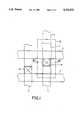
- FIG. 1is a plane view of a DRAM having a vertical transistor in accordance with the present invention.
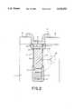
- FIG. 2is a cross-sectional view of a DRAM having a vertical transistor, taken on line II--II of FIG. 1.
- FIG. 3A through FIG. 3Gare cross-sectional views which illustrate the manufacturing steps of DRAM in accordance with the present invention.
- FIG. 1is plan view of the DRAM having a vertical transistor manufactured by the present invention.
- the cell of the DRAMis manufactured based on the folded bit line structure.
- a bit line 3is arranged lengthwise and a word line 5 is arranged horizontally so that it vertically crosses the bit line 3.
- a charge storage electrode 11 and a charge storage electrode contact 18are arranged respectively.
- the area of the unit cellbecomes 1.05 ⁇ m 2 . Accordingly, the occupation ratio of the area of the charge storage electrode respect to the area of the unit cell is 46%, which is a satisfactory value.
- FIG. 2is a cross sectional view taken on line II--II of FIG. 1. That is, the structure of the DRAM having a vertical transistor with buried bit line is illustrated. In the structure, these are first trench 30 and second trench and 40 formed sequentially in a silicon substrate 1. Also, the switching transistor of the unit cell is formed in the trench and a capacitor is formed on the top of the silicon substrate 1. The bit line 3 is formed in a second trench 40 of the substrate 1 in parallel with the surface of the substrate 1. On the top of the bit line 3, a first insulating layer 4 is formed on the bit line 3 and a word line 5 is formed on the top of the first trench 30. A channel region 6 is vertically formed respective to the surface of the substrate 1.
- a second insulating layer 7is formed between the word line 5 and a pad polysilicon layer 9.
- a charge storage electrode 11is formed on the top of the pad polysilicon 9.
- a charge storage electrode junction region 8is formed on the side wall of the pad polysilicon 9 and the second insulating layer 7 by diffusing an impurity contained in the pad polysilicon 9.
- a bit line junction region 2is formed on the side wall of the bit line 3 by diffusing an impurity from the bit line 3.
- a channel 6is formed on the wall of the second trench 40 and a signal transmitter moves from the bit line 3, via a bit line junction region 2, to the channel region 6. Then, the signal transmitter reaches the pad poly-silicon 9 via the charge storage electrode junction region 8. Finally, the signal transmitter is stored in a charge storage electrode 11.
- FIG. 3A through FIG. 3Gare cross sectional views that illustrate the manufacturing steps of the DRAM of the present invention.
- FIG. 3Ais a cross sectional view that depicts the forming of a first trench mask 11 on the top of the silicon substrate 1.
- a first trench 30 having a predetermined depthis formed by etching the exposed silicon substrate 1 using the first trench mask 12 after carrying out the process of FIG. 3A.
- the insulating layersuch as an oxide layer having a predetermined thickness is deposited over the bottom, wall, and top surfaces of the first trench 30.
- the insulating layeris etched via an anisotropic etching process to form an insulating layer spacer 13 on the wall surface of the first trench 30.
- a second trench 40 having a predetermined depthis formed by etching the exposed silicon substrate 1 of the lower part of the first trench 30, a second trench 40 having a predetermined depth is formed.
- the bit line junction region 2is formed by implanting the impurity whose type is different from that of the substrate into the lower part and the wall surface of said second trench 40. Then, the bit line poly-silicon is deposited into the first trench 30 and the second trench 40. Finally, the bit line 3 is formed by leaving the poly-silicon having a predetermined depth on the second trench 40 via an etch-back process.
- bit line junction region 2can be formed by diffusing the impurity contained in the bit line 3 after forming the bit line 3. It should be noted that the bit line junction region 2 is used as a source of the transistor.
- FIG. 3Dis a cross sectional view that illustrates the forming of the word line mask 15 on the silicon substrate 1 and the first insulating layer 4' in such a way that the word line mask 15 crosses the bit line 3 vertically after filling up to the top surface of said first trench 30 with the first insulating layer 4' such as the oxide material 4.
- a slot 20 having a predetermined depthis formed so as to form a word line 5 in the silicon substrate 1 after carrying out the process mentioned in FIG. 3D.
- the first insulating layer 4' that fills up inside of the first trench of the region where the slot 20 had been formedis removed thus exposing the first trench 30.
- the first insulating layer 4' on the top of the second trench 40is not removed and is used for the insulation between the bit line 3 and the word line 5 to be formed later.
- a gate oxide layer 14is formed on the wall surface of the first trench 30 and a word line polysilicon layer 5A is deposited over said slot 20 and inner and top surface of the first trench 30.
- word line polysilicon layer 5Ais etched to a predetermined thickness so that its height is lower than the surface of the silicon substrate 1. Finally the word line mask 15 is removed after forming the word line 5 by filling up slot 20 and said first trench with the word line polysilicon layer 5A.
- a second insulating layer 7such as an oxide layer having a predetermined thickness is formed on the top of the word line 5.
- the polysilicon layeris deposited over the top surfaces of the second insulating layer 7 and the silicon substrate 1. Having done so, leave the polysilicon up to the surface of the silicon substrate 1 of top surface of the word line 5 via an etch-back process.
- a pad polysilicon 9is created and by diffusing the impurity contained in this pad polysilicon 9 to the adjacent silicon substrate 1, thereby, a charge storage electrode junction region 8 is formed.
- the charge storage electrode junction region 8can be formed by diffusing the impurity to the exposed silicon substrate 1 of the slot 20 before forming the pad polysilicon layer 9.
- the charge storage electrode junction region 8is used as a drain of the transistor.
- a thick oxide layeris formed on the exposed silicon substrate 1 and the pad polysilicon 9.
- a contact hole 17is formed using a charge storage electrode contact mask. Then, after depositing the polysilicon layer used for the charge storage electrode 11 in the contact hole 17, the charge storage electrode 11 is formed using the charge storage electrode contact mask. Having done so, the DRAM is formed by forming a dielectric layer and a plate electrode on the top of the charge storage electrode respectively.
- a channelis formed vertically in respect to the substrate so that the channel length can be set freely without worrying about the area occupied by the cell.
- the affect of the miniaturized device that occurs in a highly integrated memory devicecan be minimized.
- the current of the transistoris increased, thereby decreasing the operation time of the semiconductor chip.
- the ratio of the storage capacitor area to the cell areais increased so that the process of forming a capacitor can be easily carried out.
Landscapes
- Engineering & Computer Science (AREA)
- Manufacturing & Machinery (AREA)
- Semiconductor Memories (AREA)
Abstract
Description
1. Field of the Invention
The invention relates to a DRAM (Dynamic Random Access Memory) of a highly integrated semiconductor device and a method of manufacturing the same, and more particularly to a DRAM having a vertical transistor whose bit line is buried in a silicon substrate and a method of manufacturing the same.
2. Related Art
Generally, the unit cell of a DRAM memory device consists of a switching transistor and a storage capacitor. As the memory device is highly integrated, the area occupied by the unit cell is reduced and thus the areas for the switching transistor and the storage capacitor must be also decreased.
Furthermore, the switching transistor is formed on the surface of the silicon substrate. In order to reduce the area of the switching transistor, the areas occupied by a source/drain and a gate of the switching transistor must be reduced. However, if areas of the source and drain are reduced, the contact process becomes difficult. Also, a serious short channel effect is produced when the gate area of the transistor is reduced. Accordingly, the area occupied by the switching transistor can be decreased only to a certain size and no more.
It is therefore an object of the present invention to provide a DRAM having a vertical transistor, which can easily reduce the area occupied by the switching transistor. The present invention accomplishes above object by providing a DRAM having a vertical transistor wherein a bit line is buried in the silicon substrate thus removing the area on the top of substrate occupied by the bit line.
Also, a word line is formed vertically on the surface of the substrate via a trench process, thereby the gate length can be elongated irrespective of the size of the unit cell thus reducing a short channel effect. Furthermore, a charge storage electrode is formed at the entrance of the trench as a stacked structure. Accordingly, on the surface of the substrate, only the charge storage electrode exists, thus, the area occupied by the charge storage electrode per unit cell can be extremely increased further unlike the conventional structure.
The preceding objects should be construed as merely presenting a few of the more pertinent features and applications of the invention. Many other beneficial results can be obtained by applying the disclosed invention in a different manner or modifying the invention within the scope of the disclosure. Accordingly, other objects and a fuller understanding of the invention may be had by referring to both the summary of the invention and the detailed description, below, which describe the preferred embodiment in addition to the scope of the invention defined by the claims considered in conjunction with the accompanying drawings.
The dynamic random access memory having a vertical transistor and the method of manufacturing such device of the present invention are defined by the claims with specific embodiments shown in the attached drawings. For the purpose of summarizing the invention, the invention relates to a dynamic random access memory having a vertical transistor comprising a silicon substrate.
Then, a word line is formed in said silicon substrate, in which said word line forms a vertical channel region and a gate oxide layer is formed on sidewall of said word line.
A bit line junction region is connected to the lower part of said channel region and is formed on the lower part of said silicon substrate and a bitline is connected to said bit line junction region and is insulated from said word line via a first insulating layer.
A charge storage electrode junction region is connected to the upper past of said channel region and is formed below the surface of said silicon substrate and a pad polysilicon layer is connected to the upper part of said charge storage electrode junction region and is insulated from said word line via the second insulating layer.
Next, a charge storage electrode is connected to said pad polysilicon layer via contact, whereby when a voltage is applied to said word line, said channel region is formed on the side wall of said word line so that the signal transmitter is mutually transferred from said bit line to said charge storage electrode.
Further, for the purpose of summarizing the invention, the invention relates to a method of manufacturing a dynamic random access memory having a vertical transistor comprising providing a silicon substrate. Then a first trench mask is formed on a desired portion of the upper portion of said substrate.
A first trench is formed by etching a desired portion of said silicon substrate, using said first trench mask and an insulating layer spacer is formed on the sidewall of said first trench by anisotropic etching process after forming an insulating layer in said first trench.
A second trench is formed in the lower part of said first trench by etching the desired portion of the exposed silicon substrate and a bit line junction region is formed on the bottom portion and the side wall of said second trench by ion implantation process.
A bitline is formed only on a desired region in said second trench via etch-back process after filling a bit line conducting layer in said first and second trench and a word line mask is formed on the desired surface of said silicon substrate after forming an oxide layer on said bit line.
A first insulating layer is formed by etching said exposed oxide layer which is positioned on the lower part of said slot to the lower past of said first trench after forming a slot by etching the desired portion of said oxide layer and the exposed silicon substrate and said word line mask positioned on said silicon substrate is removed.
A gate oxide layer is formed on the side wall of the exposed first trench and said slot and a word line having a desired thickness is formed by etch-back process after filling a word line conducting layer in said first trench and a second insulating layer is formed on said word line and a pad polysilicon is formed on said second insulating layer and a charge storage electrode junction region is formed on the outer wall of said pad polysilicon and second insulating layer by ion-implantation process.
An oxide layer is deposited over the entire structure and a contact is formed by etching a desired portion of said oxide layer, using a charge storage electrode contact mask and a charge storage electrode is formed on said contact.
The more pertinent and important features of the present invention have been outlined above in order that the detailed description of the invention which follows will be better understood and that the present contribution to the art can be fully appreciated. Additional features of the invention described hereinafter form the subject of the claims of the invention. Those skilled in the art can appreciate that the conception and the specific embodiment disclosed herein may be readily utilized as a basis for modifying or designing other structures for carrying out the same purposes of the present invention. Further, those skilled in the art can realize that such equivalent constructions do not depart from the spirit and scope of the invention as set forth in the claims.
For a fuller understanding of the nature and object of the invention, reference should be made to the following detailed description of the invention in conjunction with the accompanying drawings, in which:
FIG. 1 is a plane view of a DRAM having a vertical transistor in accordance with the present invention.
FIG. 2 is a cross-sectional view of a DRAM having a vertical transistor, taken on line II--II of FIG. 1.
FIG. 3A through FIG. 3G are cross-sectional views which illustrate the manufacturing steps of DRAM in accordance with the present invention.
The novel feature of the present invention may be understood form the accompanying description when taken in conjunction with the accompanying drawings.
Similar reference characters refer to similar parts throughout the several views of the drawings.
FIG. 1 is plan view of the DRAM having a vertical transistor manufactured by the present invention. Here, the cell of the DRAM is manufactured based on the folded bit line structure. Abit line 3 is arranged lengthwise and aword line 5 is arranged horizontally so that it vertically crosses thebit line 3. Also, acharge storage electrode 11 and a chargestorage electrode contact 18 are arranged respectively. At this time, if 0.3 μm is applied as a design rule, the area of the unit cell becomes 1.05 μm2. Accordingly, the occupation ratio of the area of the charge storage electrode respect to the area of the unit cell is 46%, which is a satisfactory value.
FIG. 2 is a cross sectional view taken on line II--II of FIG. 1. That is, the structure of the DRAM having a vertical transistor with buried bit line is illustrated. In the structure, these arefirst trench 30 and second trench and 40 formed sequentially in asilicon substrate 1. Also, the switching transistor of the unit cell is formed in the trench and a capacitor is formed on the top of thesilicon substrate 1. Thebit line 3 is formed in asecond trench 40 of thesubstrate 1 in parallel with the surface of thesubstrate 1. On the top of thebit line 3, a first insulating layer 4 is formed on thebit line 3 and aword line 5 is formed on the top of thefirst trench 30. Achannel region 6 is vertically formed respective to the surface of thesubstrate 1. A secondinsulating layer 7 is formed between theword line 5 and apad polysilicon layer 9. Acharge storage electrode 11 is formed on the top of thepad polysilicon 9. Also, a charge storageelectrode junction region 8 is formed on the side wall of thepad polysilicon 9 and the second insulatinglayer 7 by diffusing an impurity contained in thepad polysilicon 9. A bitline junction region 2 is formed on the side wall of thebit line 3 by diffusing an impurity from thebit line 3. Next, for a fuller understanding of the invention, the cell operation is described by referring to anequivalent circuit 60.
First, as in the general cell operation, if a voltage is applied to theword line 5, achannel 6 is formed on the wall of thesecond trench 40 and a signal transmitter moves from thebit line 3, via a bitline junction region 2, to thechannel region 6. Then, the signal transmitter reaches the pad poly-silicon 9 via the charge storageelectrode junction region 8. Finally, the signal transmitter is stored in acharge storage electrode 11.
FIG. 3A through FIG. 3G are cross sectional views that illustrate the manufacturing steps of the DRAM of the present invention.
FIG. 3A is a cross sectional view that depicts the forming of afirst trench mask 11 on the top of thesilicon substrate 1.
Referring to FIG. 3B, afirst trench 30 having a predetermined depth is formed by etching the exposedsilicon substrate 1 using thefirst trench mask 12 after carrying out the process of FIG. 3A. Next, the insulating layer such as an oxide layer having a predetermined thickness is deposited over the bottom, wall, and top surfaces of thefirst trench 30. Then, the insulating layer is etched via an anisotropic etching process to form an insulatinglayer spacer 13 on the wall surface of thefirst trench 30. Furthermore, by etching the exposedsilicon substrate 1 of the lower part of thefirst trench 30, asecond trench 40 having a predetermined depth is formed.
Referring to FIG. 3C, the bitline junction region 2 is formed by implanting the impurity whose type is different from that of the substrate into the lower part and the wall surface of saidsecond trench 40. Then, the bit line poly-silicon is deposited into thefirst trench 30 and thesecond trench 40. Finally, thebit line 3 is formed by leaving the poly-silicon having a predetermined depth on thesecond trench 40 via an etch-back process.
At this time, the bitline junction region 2 can be formed by diffusing the impurity contained in thebit line 3 after forming thebit line 3. It should be noted that the bitline junction region 2 is used as a source of the transistor.
FIG. 3D is a cross sectional view that illustrates the forming of theword line mask 15 on thesilicon substrate 1 and the first insulating layer 4' in such a way that theword line mask 15 crosses thebit line 3 vertically after filling up to the top surface of saidfirst trench 30 with the first insulating layer 4' such as the oxide material 4.
Referring to FIG. 3E, aslot 20 having a predetermined depth is formed so as to form aword line 5 in thesilicon substrate 1 after carrying out the process mentioned in FIG. 3D. Then, the first insulating layer 4' that fills up inside of the first trench of the region where theslot 20 had been formed is removed thus exposing thefirst trench 30. At this time, the first insulating layer 4' on the top of thesecond trench 40 is not removed and is used for the insulation between thebit line 3 and theword line 5 to be formed later. Then, agate oxide layer 14 is formed on the wall surface of thefirst trench 30 and a wordline polysilicon layer 5A is deposited over saidslot 20 and inner and top surface of thefirst trench 30. Then, wordline polysilicon layer 5A is etched to a predetermined thickness so that its height is lower than the surface of thesilicon substrate 1. Finally theword line mask 15 is removed after forming theword line 5 by filling upslot 20 and said first trench with the wordline polysilicon layer 5A.
Referring to FIG. 3F, a secondinsulating layer 7 such as an oxide layer having a predetermined thickness is formed on the top of theword line 5. Then, the polysilicon layer is deposited over the top surfaces of the second insulatinglayer 7 and thesilicon substrate 1. Having done so, leave the polysilicon up to the surface of thesilicon substrate 1 of top surface of theword line 5 via an etch-back process. Then, apad polysilicon 9 is created and by diffusing the impurity contained in thispad polysilicon 9 to theadjacent silicon substrate 1, thereby, a charge storageelectrode junction region 8 is formed. It should be noted that the charge storageelectrode junction region 8 can be formed by diffusing the impurity to the exposedsilicon substrate 1 of theslot 20 before forming thepad polysilicon layer 9.
Here, the charge storageelectrode junction region 8 is used as a drain of the transistor.
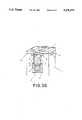
Referring to FIG. 3G, after completing the process of FIG. 3F, a thick oxide layer is formed on the exposedsilicon substrate 1 and thepad polysilicon 9.
Also, acontact hole 17 is formed using a charge storage electrode contact mask. Then, after depositing the polysilicon layer used for thecharge storage electrode 11 in thecontact hole 17, thecharge storage electrode 11 is formed using the charge storage electrode contact mask. Having done so, the DRAM is formed by forming a dielectric layer and a plate electrode on the top of the charge storage electrode respectively.
As discussed so far, when manufacturing the DRAM of the present invention, a channel is formed vertically in respect to the substrate so that the channel length can be set freely without worrying about the area occupied by the cell. Thus, the affect of the miniaturized device that occurs in a highly integrated memory device can be minimized. Also, since two channels are available, the current of the transistor is increased, thereby decreasing the operation time of the semiconductor chip.
Furthermore, since there is only the charge storage capacitor on the surface of thesilicon substrate 1, the ratio of the storage capacitor area to the cell area is increased so that the process of forming a capacitor can be easily carried out.
Although this invention has been described in its preferred form with a certain degree of particularity, it is appreciated by those skilled in the art that the present disclosure of the preferred form has been made only by way of example and that numerous changes in the details of the construction, combination and arrangement of parts may be resorted to without departing from the spirit and scope of the invention.
Claims (8)
1. A method of manufacturing a dynamic random access memory having a vertical transistor, comprising the steps of:
providing a silicon substrate having a planar substrate surface;
forming a first trench mask on said substrate surface, said first trench mask comprising a pair of sections extending in the same direction from an edge of said substrate surface, said sections of said first trench mask being separated by a portion of said substrate surface constituting a trench portion;
etching said trench portion to form a first trench;
forming an insulating layer in said first trench;
anisotropically etching the insulating layer to form an insulating layer spacer on an interior side wall of said first trench;
etching an interior bottom of said first trench to form a second trench;
implanting ions on an interior bottom portion and a side wall of said second trench to form a bit line junction region;
filling said first and second trenches with a bit line conducting layer;
etching back said bit line conducting layer to form a bit line in said second trench below said first trench;
forming a first oxide layer on said bit line, first trench, and substrate surface;
forming a word line mask on said substrate surface on one side of said first trench, said word line mask comprising a pair of sections extending in the same direction from one side wall of said first trench, said sections of said word line mask being separated by a portion of said substrate surface constituting a slot portion;
etching said slot portion and first oxide layer thereon to form a slot intersecting said first trench;
etching said first oxide layer on an interior bottom of said slot to an interior bottom of said first trench to form a first insulating layer;
removing said word line mask from said substrate surface;
forming a gate oxide layer on an interior side wall of said first trench and slot;
filling a word line conducting layer in said first trench;
etching back said word line conducting layer to an elevation below said substrate surface to form a word line;
forming a second insulating layer on said word line, said second insulating layer being below said substrate surface;
forming an electrode contact on said second insulating layer, said electrode contact comprising a pad polysilicon on said second insulating layer and charge storage electrode junction region adjoining sides of said pad polysilicon and second insulating layer, said charge storage electrode junction region being formed by ion-implantation;
depositing a second oxide layer on said pad polysilicon and substrate surface;
forming a charge storage electrode contact mask on a portion of said second oxide layer, said contact mask enclosing another portion of said second oxide layer formed on said pad polysilicon;
etching said another portion of said second oxide layer to form a contact hole; and
forming a charge storage electrode in said contact hole.
2. The method of claim 1, wherein said pad polysilicon is formed on said second insulating layer before forming said charge storage electrode junction region.
3. The method according to claim 1, wherein said bit line conducting layer is formed of polysilicon.
4. The method of claim 1, wherein said charge storage electrode junction region is formed by diffusing an impurity contained in said pad polysilicon to said silicon substrate.
5. The method of claim 1, wherein said charge storage electrode junction region is formed before forming said pad polysilicon on said second insulating layer.
6. The method of claim 5, wherein said charge storage electrode junction region is formed by diffusing an impurity, via said slot, to a portion of said silicon substrate containing adjoining portions of said substrate surface and said interior side wall of said first trench.
7. The method of claim 1, wherein said bit line junction region is used as a source of the transistor.
8. The method of claim 1, wherein said charge storage electrode junction region is used as a drain of the transistor.
Priority Applications (1)
| Application Number | Priority Date | Filing Date | Title |
|---|---|---|---|
| US08/269,218US5504357A (en) | 1991-09-26 | 1994-06-30 | Dynamic random access memory having a vertical transistor |
Applications Claiming Priority (2)
| Application Number | Priority Date | Filing Date | Title |
|---|---|---|---|
| KR1019910016756AKR940006679B1 (en) | 1991-09-26 | 1991-09-26 | Dram cell having a vertical transistor and fabricating method thereof |
| KR91-16756 | 1991-09-26 |
Related Child Applications (1)
| Application Number | Title | Priority Date | Filing Date |
|---|---|---|---|
| US08/269,218DivisionUS5504357A (en) | 1991-09-26 | 1994-06-30 | Dynamic random access memory having a vertical transistor |
Publications (1)
| Publication Number | Publication Date |
|---|---|
| US5376575Atrue US5376575A (en) | 1994-12-27 |
Family
ID=19320352
Family Applications (2)
| Application Number | Title | Priority Date | Filing Date |
|---|---|---|---|
| US07/951,174Expired - LifetimeUS5376575A (en) | 1991-09-26 | 1992-09-24 | Method of making dynamic random access memory having a vertical transistor |
| US08/269,218Expired - Fee RelatedUS5504357A (en) | 1991-09-26 | 1994-06-30 | Dynamic random access memory having a vertical transistor |
Family Applications After (1)
| Application Number | Title | Priority Date | Filing Date |
|---|---|---|---|
| US08/269,218Expired - Fee RelatedUS5504357A (en) | 1991-09-26 | 1994-06-30 | Dynamic random access memory having a vertical transistor |
Country Status (3)
| Country | Link |
|---|---|
| US (2) | US5376575A (en) |
| JP (1) | JPH0799769B2 (en) |
| KR (1) | KR940006679B1 (en) |
Cited By (60)
| Publication number | Priority date | Publication date | Assignee | Title |
|---|---|---|---|---|
| DE19519160C1 (en)* | 1995-05-24 | 1996-09-12 | Siemens Ag | DRAM cell arrangement having packing density required for specified memory |
| EP0744772A1 (en)* | 1995-05-24 | 1996-11-27 | Siemens Aktiengesellschaft | DRAM storage cell with vertical transistor and method for production thereof |
| US5792690A (en)* | 1997-05-15 | 1998-08-11 | Vanguard International Semiconductor Corporation | Method of fabricating a DRAM cell with an area equal to four times the used minimum feature |
| DE19720193A1 (en)* | 1997-05-14 | 1998-11-19 | Siemens Ag | Vertical metal-oxide-semiconductor transistor integrated circuit |
| US5907170A (en)* | 1997-10-06 | 1999-05-25 | Micron Technology, Inc. | Circuit and method for an open bit line memory cell with a vertical transistor and trench plate trench capacitor |
| US5909618A (en)* | 1997-07-08 | 1999-06-01 | Micron Technology, Inc. | Method of making memory cell with vertical transistor and buried word and body lines |
| US5914511A (en)* | 1997-10-06 | 1999-06-22 | Micron Technology, Inc. | Circuit and method for a folded bit line memory using trench plate capacitor cells with body bias contacts |
| US5937296A (en)* | 1996-12-20 | 1999-08-10 | Siemens Aktiengesellschaft | Memory cell that includes a vertical transistor and a trench capacitor |
| US5936274A (en)* | 1997-07-08 | 1999-08-10 | Micron Technology, Inc. | High density flash memory |
| US5963469A (en)* | 1998-02-24 | 1999-10-05 | Micron Technology, Inc. | Vertical bipolar read access for low voltage memory cell |
| US5973356A (en)* | 1997-07-08 | 1999-10-26 | Micron Technology, Inc. | Ultra high density flash memory |
| US5991225A (en)* | 1998-02-27 | 1999-11-23 | Micron Technology, Inc. | Programmable memory address decode array with vertical transistors |
| US5998253A (en)* | 1997-09-29 | 1999-12-07 | Siemens Aktiengesellschaft | Method of forming a dopant outdiffusion control structure including selectively grown silicon nitride in a trench capacitor of a DRAM cell |
| US6025225A (en)* | 1998-01-22 | 2000-02-15 | Micron Technology, Inc. | Circuits with a trench capacitor having micro-roughened semiconductor surfaces and methods for forming the same |
| US6043527A (en)* | 1998-04-14 | 2000-03-28 | Micron Technology, Inc. | Circuits and methods for a memory cell with a trench plate trench capacitor and a vertical bipolar read device |
| WO2000019525A1 (en)* | 1998-09-30 | 2000-04-06 | Infineon Technologies Ag | Substrate with an indentation for an integrated circuit device and method for the production thereof |
| DE19844997A1 (en)* | 1998-09-30 | 2000-04-13 | Siemens Ag | Vertical field effect transistor with internal gate and manufacturing process |
| US6066869A (en)* | 1997-10-06 | 2000-05-23 | Micron Technology, Inc. | Circuit and method for a folded bit line memory cell with vertical transistor and trench capacitor |
| US6072209A (en)* | 1997-07-08 | 2000-06-06 | Micro Technology, Inc. | Four F2 folded bit line DRAM cell structure having buried bit and word lines |
| US6093623A (en)* | 1998-08-04 | 2000-07-25 | Micron Technology, Inc. | Methods for making silicon-on-insulator structures |
| US6124729A (en)* | 1998-02-27 | 2000-09-26 | Micron Technology, Inc. | Field programmable logic arrays with vertical transistors |
| US6134175A (en)* | 1998-08-04 | 2000-10-17 | Micron Technology, Inc. | Memory address decode array with vertical transistors |
| US6150687A (en)* | 1997-07-08 | 2000-11-21 | Micron Technology, Inc. | Memory cell having a vertical transistor with buried source/drain and dual gates |
| US6156604A (en)* | 1997-10-06 | 2000-12-05 | Micron Technology, Inc. | Method for making an open bit line memory cell with a vertical transistor and trench plate trench capacitor |
| US6172391B1 (en) | 1997-08-27 | 2001-01-09 | Siemens Aktiengesellschaft | DRAM cell arrangement and method for the manufacture thereof |
| US6191470B1 (en) | 1997-07-08 | 2001-02-20 | Micron Technology, Inc. | Semiconductor-on-insulator memory cell with buried word and body lines |
| US6208164B1 (en) | 1998-08-04 | 2001-03-27 | Micron Technology, Inc. | Programmable logic array with vertical transistors |
| US6242775B1 (en) | 1998-02-24 | 2001-06-05 | Micron Technology, Inc. | Circuits and methods using vertical complementary transistors |
| US6246083B1 (en) | 1998-02-24 | 2001-06-12 | Micron Technology, Inc. | Vertical gain cell and array for a dynamic random access memory |
| US6255684B1 (en) | 1997-05-02 | 2001-07-03 | Infineon Technologies Ag | DRAM cell configuration and method for its production |
| US6265279B1 (en)* | 1999-09-24 | 2001-07-24 | Infineon Technologies Ag | Method for fabricating a trench capacitor |
| US6274437B1 (en)* | 1995-06-14 | 2001-08-14 | Totem Semiconductor Limited | Trench gated power device fabrication by doping side walls of partially filled trench |
| US6304483B1 (en) | 1998-02-24 | 2001-10-16 | Micron Technology, Inc. | Circuits and methods for a static random access memory using vertical transistors |
| US6417091B2 (en)* | 1997-12-22 | 2002-07-09 | Texas Instruments Incorporated | Mask and method for forming dynamic random access memory (DRAM) contacts |
| US6420239B2 (en)* | 2000-05-31 | 2002-07-16 | Infineon Technologies Ag | Memory cell with trench capacitor and method of fabricating the memory cell |
| US6423613B1 (en) | 1998-11-10 | 2002-07-23 | Micron Technology, Inc. | Low temperature silicon wafer bond process with bulk material bond strength |
| US6504200B2 (en)* | 1999-03-12 | 2003-01-07 | Infineon Technologies Ag | DRAM cell configuration and fabrication method |
| US6566187B1 (en)* | 1998-09-30 | 2003-05-20 | Infineon Technologies Ag | DRAM cell system and method for producing same |
| US6570207B2 (en) | 2000-12-13 | 2003-05-27 | International Business Machines Corporation | Structure and method for creating vertical capacitor and anti-fuse in DRAM process employing vertical array device cell complex |
| US20040018695A1 (en)* | 2002-07-26 | 2004-01-29 | Tang Sanh D. | Methods of forming trench isolation within a semiconductor substrate |
| US6852167B2 (en) | 2001-03-01 | 2005-02-08 | Micron Technology, Inc. | Methods, systems, and apparatus for uniform chemical-vapor depositions |
| US20060043449A1 (en)* | 2004-09-01 | 2006-03-02 | Tang Sanh D | Semiconductor constructions and transistors, and methods of forming semiconductor constructions and transistors |
| US20060046391A1 (en)* | 2004-08-30 | 2006-03-02 | Tang Sanh D | Vertical wrap-around-gate field-effect-transistor for high density, low voltage logic and memory array |
| US7160577B2 (en) | 2002-05-02 | 2007-01-09 | Micron Technology, Inc. | Methods for atomic-layer deposition of aluminum oxides in integrated circuits |
| US20080108791A1 (en)* | 2004-02-02 | 2008-05-08 | Ambrx, Inc. | Modified Human Interferon Polypeptides and Their Uses |
| US20080173936A1 (en)* | 2007-01-18 | 2008-07-24 | Samsung Electronics Co., Ltd. | Access device having vertical channel and related semiconductor device and a method of fabricating the access device |
| US7560793B2 (en) | 2002-05-02 | 2009-07-14 | Micron Technology, Inc. | Atomic layer deposition and conversion |
| US20090256194A1 (en)* | 2008-04-10 | 2009-10-15 | Kyung Do Kim | Semiconductor device with reduced resistance of bit lines and method for manufacturing the same |
| US7700441B2 (en) | 2006-02-02 | 2010-04-20 | Micron Technology, Inc. | Methods of forming field effect transistors, methods of forming field effect transistor gates, methods of forming integrated circuitry comprising a transistor gate array and circuitry peripheral to the gate array, and methods of forming integrated circuitry comprising a transistor gate array including first gates and second grounded isolation gates |
| US7772632B2 (en) | 2006-08-21 | 2010-08-10 | Micron Technology, Inc. | Memory arrays and methods of fabricating memory arrays |
| US7867851B2 (en) | 2005-08-30 | 2011-01-11 | Micron Technology, Inc. | Methods of forming field effect transistors on substrates |
| US7897460B2 (en) | 2005-03-25 | 2011-03-01 | Micron Technology, Inc. | Methods of forming recessed access devices associated with semiconductor constructions |
| CN102034824A (en)* | 2009-09-24 | 2011-04-27 | 三星电子株式会社 | Semiconductor device comprising buried word lines |
| US7944743B2 (en) | 2006-09-07 | 2011-05-17 | Micron Technology, Inc. | Methods of making a semiconductor memory device |
| US20120061724A1 (en)* | 2010-09-15 | 2012-03-15 | Kabushiki Kaisha Toshiba | Semiconductor device |
| US8399920B2 (en) | 2005-07-08 | 2013-03-19 | Werner Juengling | Semiconductor device comprising a transistor gate having multiple vertically oriented sidewalls |
| US8501563B2 (en) | 2005-07-20 | 2013-08-06 | Micron Technology, Inc. | Devices with nanocrystals and methods of formation |
| US8551823B2 (en) | 2006-07-17 | 2013-10-08 | Micron Technology, Inc. | Methods of forming lines of capacitorless one transistor DRAM cells, methods of patterning substrates, and methods of forming two conductive lines |
| US20140332885A1 (en)* | 2004-10-29 | 2014-11-13 | Infineon Technologies Ag | Trench Transistor Having a Doped Semiconductor Region |
| US10515801B2 (en) | 2007-06-04 | 2019-12-24 | Micron Technology, Inc. | Pitch multiplication using self-assembling materials |
Families Citing this family (22)
| Publication number | Priority date | Publication date | Assignee | Title |
|---|---|---|---|---|
| KR0147584B1 (en)* | 1994-03-17 | 1998-08-01 | 윤종용 | Method of manufacturing buried bitline cell |
| US5717628A (en)* | 1996-03-04 | 1998-02-10 | Siemens Aktiengesellschaft | Nitride cap formation in a DRAM trench capacitor |
| US6163052A (en)* | 1997-04-04 | 2000-12-19 | Advanced Micro Devices, Inc. | Trench-gated vertical combination JFET and MOSFET devices |
| TW399301B (en)* | 1998-04-18 | 2000-07-21 | United Microelectronics Corp | Manufacturing method of bit line |
| US6025261A (en) | 1998-04-29 | 2000-02-15 | Micron Technology, Inc. | Method for making high-Q inductive elements |
| US6696746B1 (en) | 1998-04-29 | 2004-02-24 | Micron Technology, Inc. | Buried conductors |
| US6074909A (en)* | 1998-07-31 | 2000-06-13 | Siemens Aktiengesellschaft | Apparatus and method for forming controlled deep trench top isolation layers |
| US5977579A (en)* | 1998-12-03 | 1999-11-02 | Micron Technology, Inc. | Trench dram cell with vertical device and buried word lines |
| US6690038B1 (en) | 1999-06-05 | 2004-02-10 | T-Ram, Inc. | Thyristor-based device over substrate surface |
| US6426252B1 (en) | 1999-10-25 | 2002-07-30 | International Business Machines Corporation | Silicon-on-insulator vertical array DRAM cell with self-aligned buried strap |
| US6566177B1 (en) | 1999-10-25 | 2003-05-20 | International Business Machines Corporation | Silicon-on-insulator vertical array device trench capacitor DRAM |
| KR100355097B1 (en)* | 2000-05-13 | 2002-10-11 | 주식회사 이스트웰 | The stabilizing method of coloring dyes for pulp |
| US6455886B1 (en) | 2000-08-10 | 2002-09-24 | International Business Machines Corporation | Structure and process for compact cell area in a stacked capacitor cell array |
| JP2002094027A (en)* | 2000-09-11 | 2002-03-29 | Toshiba Corp | Semiconductor memory device and manufacturing method thereof |
| US6683346B2 (en)* | 2001-03-09 | 2004-01-27 | Fairchild Semiconductor Corporation | Ultra dense trench-gated power-device with the reduced drain-source feedback capacitance and Miller charge |
| US6727528B1 (en) | 2001-03-22 | 2004-04-27 | T-Ram, Inc. | Thyristor-based device including trench dielectric isolation for thyristor-body regions |
| US7456439B1 (en) | 2001-03-22 | 2008-11-25 | T-Ram Semiconductor, Inc. | Vertical thyristor-based memory with trench isolation and its method of fabrication |
| US6624515B1 (en) | 2002-03-11 | 2003-09-23 | Micron Technology, Inc. | Microelectronic die including low RC under-layer interconnects |
| JP2008218514A (en)* | 2007-02-28 | 2008-09-18 | Toshiba Corp | Magnetic random access memory and manufacturing method thereof |
| JP2009224543A (en)* | 2008-03-17 | 2009-10-01 | Sony Corp | Method for production of semiconductor device |
| KR101131967B1 (en)* | 2010-01-29 | 2012-04-05 | 주식회사 하이닉스반도체 | Semiconductor device with vertical channel and method for manufacturing the same |
| CN103367309B (en)* | 2012-03-31 | 2016-06-22 | 南亚科技股份有限公司 | Through-silicon via with control electrode and fabrication method thereof |
Citations (5)
| Publication number | Priority date | Publication date | Assignee | Title |
|---|---|---|---|---|
| JPS58213464A (en)* | 1982-06-04 | 1983-12-12 | Nec Corp | Semiconductor device |
| US4672410A (en)* | 1984-07-12 | 1987-06-09 | Nippon Telegraph & Telephone | Semiconductor memory device with trench surrounding each memory cell |
| US4689871A (en)* | 1985-09-24 | 1987-09-01 | Texas Instruments Incorporated | Method of forming vertically integrated current source |
| JPH01248557A (en)* | 1988-03-29 | 1989-10-04 | Toshiba Corp | Semiconductor storage device and its manufacturing method |
| JPH03218665A (en)* | 1990-01-24 | 1991-09-26 | Matsushita Electric Ind Co Ltd | Semiconductor memory device and manufacture thereof |
Family Cites Families (3)
| Publication number | Priority date | Publication date | Assignee | Title |
|---|---|---|---|---|
| JPH0793365B2 (en)* | 1984-09-11 | 1995-10-09 | 株式会社東芝 | Semiconductor memory device and manufacturing method thereof |
| JPH01307260A (en)* | 1988-06-03 | 1989-12-12 | Matsushita Electric Ind Co Ltd | semiconductor memory cell |
| JP2932635B2 (en)* | 1990-08-11 | 1999-08-09 | 日本電気株式会社 | Semiconductor storage device |
- 1991
- 1991-09-26KRKR1019910016756Apatent/KR940006679B1/ennot_activeExpired - Fee Related
- 1992
- 1992-09-24USUS07/951,174patent/US5376575A/ennot_activeExpired - Lifetime
- 1992-09-25JPJP4256409Apatent/JPH0799769B2/ennot_activeExpired - Fee Related
- 1994
- 1994-06-30USUS08/269,218patent/US5504357A/ennot_activeExpired - Fee Related
Patent Citations (5)
| Publication number | Priority date | Publication date | Assignee | Title |
|---|---|---|---|---|
| JPS58213464A (en)* | 1982-06-04 | 1983-12-12 | Nec Corp | Semiconductor device |
| US4672410A (en)* | 1984-07-12 | 1987-06-09 | Nippon Telegraph & Telephone | Semiconductor memory device with trench surrounding each memory cell |
| US4689871A (en)* | 1985-09-24 | 1987-09-01 | Texas Instruments Incorporated | Method of forming vertically integrated current source |
| JPH01248557A (en)* | 1988-03-29 | 1989-10-04 | Toshiba Corp | Semiconductor storage device and its manufacturing method |
| JPH03218665A (en)* | 1990-01-24 | 1991-09-26 | Matsushita Electric Ind Co Ltd | Semiconductor memory device and manufacture thereof |
Cited By (151)
| Publication number | Priority date | Publication date | Assignee | Title |
|---|---|---|---|---|
| DE19519160C1 (en)* | 1995-05-24 | 1996-09-12 | Siemens Ag | DRAM cell arrangement having packing density required for specified memory |
| EP0744772A1 (en)* | 1995-05-24 | 1996-11-27 | Siemens Aktiengesellschaft | DRAM storage cell with vertical transistor and method for production thereof |
| DE19519159A1 (en)* | 1995-05-24 | 1996-11-28 | Siemens Ag | DRAM cell arrangement and method for its production |
| US5736761A (en)* | 1995-05-24 | 1998-04-07 | Siemens Aktiengesellschaft | DRAM cell arrangement and method for its manufacture |
| DE19519159C2 (en)* | 1995-05-24 | 1998-07-09 | Siemens Ag | DRAM cell arrangement and method for its production |
| US6274437B1 (en)* | 1995-06-14 | 2001-08-14 | Totem Semiconductor Limited | Trench gated power device fabrication by doping side walls of partially filled trench |
| US5937296A (en)* | 1996-12-20 | 1999-08-10 | Siemens Aktiengesellschaft | Memory cell that includes a vertical transistor and a trench capacitor |
| US6420228B1 (en) | 1997-05-02 | 2002-07-16 | Infineon Technologies Ag | Method for the production of a DRAM cell configuration |
| US6255684B1 (en) | 1997-05-02 | 2001-07-03 | Infineon Technologies Ag | DRAM cell configuration and method for its production |
| DE19720193A1 (en)* | 1997-05-14 | 1998-11-19 | Siemens Ag | Vertical metal-oxide-semiconductor transistor integrated circuit |
| US6376313B1 (en) | 1997-05-14 | 2002-04-23 | Siemens Aktiengesellschaft | Integrated circuit having at least two vertical MOS transistors and method for manufacturing same |
| DE19720193C2 (en)* | 1997-05-14 | 2002-10-17 | Infineon Technologies Ag | Integrated circuit arrangement with at least two vertical MOS transistors and method for their production |
| US6566202B2 (en) | 1997-05-14 | 2003-05-20 | Siemens Aktiengesellschaft | Integrated circuit having at least two vertical MOS transistors and method for manufacturing same |
| US5792690A (en)* | 1997-05-15 | 1998-08-11 | Vanguard International Semiconductor Corporation | Method of fabricating a DRAM cell with an area equal to four times the used minimum feature |
| US6689660B1 (en) | 1997-07-08 | 2004-02-10 | Micron Technology, Inc. | 4 F2 folded bit line DRAM cell structure having buried bit and word lines |
| US6191448B1 (en) | 1997-07-08 | 2001-02-20 | Micron Technology, Inc. | Memory cell with vertical transistor and buried word and body lines |
| US6399979B1 (en) | 1997-07-08 | 2002-06-04 | Micron Technology, Inc. | Memory cell having a vertical transistor with buried source/drain and dual gates |
| US6465298B2 (en) | 1997-07-08 | 2002-10-15 | Micron Technology, Inc. | Method of fabricating a semiconductor-on-insulator memory cell with buried word and body lines |
| US6350635B1 (en) | 1997-07-08 | 2002-02-26 | Micron Technology, Inc. | Memory cell having a vertical transistor with buried source/drain and dual gates |
| US5909618A (en)* | 1997-07-08 | 1999-06-01 | Micron Technology, Inc. | Method of making memory cell with vertical transistor and buried word and body lines |
| US6476434B1 (en) | 1997-07-08 | 2002-11-05 | Micron Tecnology, Inc. | 4 F2 folded bit line dram cell structure having buried bit and word lines |
| US6072209A (en)* | 1997-07-08 | 2000-06-06 | Micro Technology, Inc. | Four F2 folded bit line DRAM cell structure having buried bit and word lines |
| US6492233B2 (en) | 1997-07-08 | 2002-12-10 | Micron Technology, Inc. | Memory cell with vertical transistor and buried word and body lines |
| US6104061A (en)* | 1997-07-08 | 2000-08-15 | Micron Technology, Inc. | Memory cell with vertical transistor and buried word and body lines |
| US6818937B2 (en) | 1997-07-08 | 2004-11-16 | Micron Technology, Inc. | Memory cell having a vertical transistor with buried source/drain and dual gates |
| US5973356A (en)* | 1997-07-08 | 1999-10-26 | Micron Technology, Inc. | Ultra high density flash memory |
| US6143636A (en)* | 1997-07-08 | 2000-11-07 | Micron Technology, Inc. | High density flash memory |
| US6150687A (en)* | 1997-07-08 | 2000-11-21 | Micron Technology, Inc. | Memory cell having a vertical transistor with buried source/drain and dual gates |
| US6504201B1 (en) | 1997-07-08 | 2003-01-07 | Micron Technology, Inc. | Memory cell having a vertical transistor with buried source/drain and dual gates |
| US5936274A (en)* | 1997-07-08 | 1999-08-10 | Micron Technology, Inc. | High density flash memory |
| US6191470B1 (en) | 1997-07-08 | 2001-02-20 | Micron Technology, Inc. | Semiconductor-on-insulator memory cell with buried word and body lines |
| EP0899790A3 (en)* | 1997-08-27 | 2006-02-08 | Infineon Technologies AG | DRAM cell array and method of producing the same |
| US6172391B1 (en) | 1997-08-27 | 2001-01-09 | Siemens Aktiengesellschaft | DRAM cell arrangement and method for the manufacture thereof |
| US5998253A (en)* | 1997-09-29 | 1999-12-07 | Siemens Aktiengesellschaft | Method of forming a dopant outdiffusion control structure including selectively grown silicon nitride in a trench capacitor of a DRAM cell |
| US6764901B2 (en) | 1997-10-06 | 2004-07-20 | Micron Technology, Inc. | Circuit and method for a folded bit line memory cell with vertical transistor and trench capacitor |
| US5907170A (en)* | 1997-10-06 | 1999-05-25 | Micron Technology, Inc. | Circuit and method for an open bit line memory cell with a vertical transistor and trench plate trench capacitor |
| US6528837B2 (en) | 1997-10-06 | 2003-03-04 | Micron Technology, Inc. | Circuit and method for an open bit line memory cell with a vertical transistor and trench plate trench capacitor |
| US6156607A (en)* | 1997-10-06 | 2000-12-05 | Micron Technology, Inc. | Method for a folded bit line memory using trench plate capacitor cells with body bias contacts |
| US6156604A (en)* | 1997-10-06 | 2000-12-05 | Micron Technology, Inc. | Method for making an open bit line memory cell with a vertical transistor and trench plate trench capacitor |
| US7057223B2 (en) | 1997-10-06 | 2006-06-06 | Micron Technology, Inc | Circuit and method for a folded bit line memory cell with vertical transistor and trench capacitor |
| US5914511A (en)* | 1997-10-06 | 1999-06-22 | Micron Technology, Inc. | Circuit and method for a folded bit line memory using trench plate capacitor cells with body bias contacts |
| US6165836A (en)* | 1997-10-06 | 2000-12-26 | Micron Technology, Inc. | Circuit and method for an open bit line memory cell with a vertical transistor and trench plate trench capacitor |
| US6610566B2 (en) | 1997-10-06 | 2003-08-26 | Micron Technology, Inc. | Circuit and method for an open bit line memory cell with a vertical transistor and trench plate trench capacitor |
| US6066869A (en)* | 1997-10-06 | 2000-05-23 | Micron Technology, Inc. | Circuit and method for a folded bit line memory cell with vertical transistor and trench capacitor |
| US6798009B2 (en) | 1997-10-06 | 2004-09-28 | Micron Technology, Inc. | Circuit and method for an open bit line memory cell with a vertical transistor and trench plate trench capacitor |
| US7223678B2 (en) | 1997-10-06 | 2007-05-29 | Micron Technology, Inc. | Circuit and method for a folded bit line memory cell with vertical transistor and trench capacitor |
| US6537871B2 (en) | 1997-10-06 | 2003-03-25 | Micron Technology, Inc. | Circuit and method for an open bit line memory cell with a vertical transistor and trench plate trench capacitor |
| US6417091B2 (en)* | 1997-12-22 | 2002-07-09 | Texas Instruments Incorporated | Mask and method for forming dynamic random access memory (DRAM) contacts |
| US7408216B2 (en) | 1998-01-22 | 2008-08-05 | Micron Technology, Inc. | Device, system, and method for a trench capacitor having micro-roughened semiconductor surfaces |
| US20010035549A1 (en)* | 1998-01-22 | 2001-11-01 | Leonard Forbes | Circuits with a trench capacitor having micro-roughened semiconductor surfaces |
| US6025225A (en)* | 1998-01-22 | 2000-02-15 | Micron Technology, Inc. | Circuits with a trench capacitor having micro-roughened semiconductor surfaces and methods for forming the same |
| US7084451B2 (en) | 1998-01-22 | 2006-08-01 | Micron Technology, Inc. | Circuits with a trench capacitor having micro-roughened semiconductor surfaces |
| US6304483B1 (en) | 1998-02-24 | 2001-10-16 | Micron Technology, Inc. | Circuits and methods for a static random access memory using vertical transistors |
| US6756622B2 (en) | 1998-02-24 | 2004-06-29 | Micron Technology, Inc. | Vertical gain cell and array for a dynamic random access memory and method for forming the same |
| US7049196B2 (en) | 1998-02-24 | 2006-05-23 | Micron Technology, Inc. | Vertical gain cell and array for a dynamic random access memory and method for forming the same |
| US5963469A (en)* | 1998-02-24 | 1999-10-05 | Micron Technology, Inc. | Vertical bipolar read access for low voltage memory cell |
| US6777744B2 (en) | 1998-02-24 | 2004-08-17 | Micron Technology, Inc. | Circuits and methods using vertical, complementary transistors |
| US6449186B2 (en) | 1998-02-24 | 2002-09-10 | Micron Technology, Inc. | Circuits and methods for a static random access memory using vertical transistors |
| US6680864B2 (en) | 1998-02-24 | 2004-01-20 | Micron Technology, Inc. | Method for reading a vertical gain cell and array for a dynamic random access memory |
| US6317357B1 (en) | 1998-02-24 | 2001-11-13 | Micron Technology, Inc. | Vertical bipolar read access for low voltage memory cell |
| US6242775B1 (en) | 1998-02-24 | 2001-06-05 | Micron Technology, Inc. | Circuits and methods using vertical complementary transistors |
| US6477080B2 (en) | 1998-02-24 | 2002-11-05 | Micron Technology, Inc. | Circuits and methods for a static random access memory using vertical transistors |
| US6246083B1 (en) | 1998-02-24 | 2001-06-12 | Micron Technology, Inc. | Vertical gain cell and array for a dynamic random access memory |
| US6294418B1 (en) | 1998-02-24 | 2001-09-25 | Micron Technology, Inc. | Circuits and methods using vertical complementary transistors |
| US6124729A (en)* | 1998-02-27 | 2000-09-26 | Micron Technology, Inc. | Field programmable logic arrays with vertical transistors |
| US6597037B1 (en) | 1998-02-27 | 2003-07-22 | Micron Technology, Inc. | Programmable memory address decode array with vertical transistors |
| US6486027B1 (en) | 1998-02-27 | 2002-11-26 | Micron Technology, Inc. | Field programmable logic arrays with vertical transistors |
| US5991225A (en)* | 1998-02-27 | 1999-11-23 | Micron Technology, Inc. | Programmable memory address decode array with vertical transistors |
| US6153468A (en)* | 1998-02-27 | 2000-11-28 | Micron Technololgy, Inc. | Method of forming a logic array for a decoder |
| US6812516B2 (en) | 1998-02-27 | 2004-11-02 | Micron Technology, Inc. | Field programmable logic arrays with vertical transistors |
| US6429065B2 (en) | 1998-04-14 | 2002-08-06 | Micron Technology, Inc. | Circuits and methods for a memory cell with a trench plate trench capacitor and a vertical bipolar read device |
| US6434041B2 (en) | 1998-04-14 | 2002-08-13 | Micron Technology, Inc. | Circuits and methods for a memory cell with a trench plate trench capacitor and a vertical bipolar read device |
| US6381168B2 (en) | 1998-04-14 | 2002-04-30 | Micron Technology, Inc. | Circuits and methods for a memory cell with a trench plate trench capacitor and a vertical bipolar read device |
| US6043527A (en)* | 1998-04-14 | 2000-03-28 | Micron Technology, Inc. | Circuits and methods for a memory cell with a trench plate trench capacitor and a vertical bipolar read device |
| US6418050B2 (en) | 1998-04-14 | 2002-07-09 | Micron Technology, Inc. | Circuits and methods for a memory cell with a trench plate trench capacitor and a vertical bipolar read device |
| US6134175A (en)* | 1998-08-04 | 2000-10-17 | Micron Technology, Inc. | Memory address decode array with vertical transistors |
| US6498065B1 (en) | 1998-08-04 | 2002-12-24 | Micron Technology, Inc. | Memory address decode array with vertical transistors |
| US6093623A (en)* | 1998-08-04 | 2000-07-25 | Micron Technology, Inc. | Methods for making silicon-on-insulator structures |
| US6208164B1 (en) | 1998-08-04 | 2001-03-27 | Micron Technology, Inc. | Programmable logic array with vertical transistors |
| US6538330B1 (en) | 1998-08-04 | 2003-03-25 | Micron Technology, Inc. | Multilevel semiconductor-on-insulator structures and circuits |
| US6309950B1 (en) | 1998-08-04 | 2001-10-30 | Micron Technology, Inc. | Methods for making silicon-on-insulator structures |
| US6515510B2 (en) | 1998-08-04 | 2003-02-04 | Micron Technology, Inc. | Programmable logic array with vertical transistors |
| US6486703B2 (en) | 1998-08-04 | 2002-11-26 | Micron Technology, Inc. | Programmable logic array with vertical transistors |
| US6747305B2 (en) | 1998-08-04 | 2004-06-08 | Micron Technology, Inc. | Memory address decode array with vertical transistors |
| US6566187B1 (en)* | 1998-09-30 | 2003-05-20 | Infineon Technologies Ag | DRAM cell system and method for producing same |
| WO2000019525A1 (en)* | 1998-09-30 | 2000-04-06 | Infineon Technologies Ag | Substrate with an indentation for an integrated circuit device and method for the production thereof |
| US6608340B1 (en) | 1998-09-30 | 2003-08-19 | Infineon Technologies Ag | Substrate assembly having a depression suitable for an integrated circuit configuration and method for its fabrication |
| DE19844997A1 (en)* | 1998-09-30 | 2000-04-13 | Siemens Ag | Vertical field effect transistor with internal gate and manufacturing process |
| US6630713B2 (en) | 1998-11-10 | 2003-10-07 | Micron Technology, Inc. | Low temperature silicon wafer bond process with bulk material bond strength |
| US6423613B1 (en) | 1998-11-10 | 2002-07-23 | Micron Technology, Inc. | Low temperature silicon wafer bond process with bulk material bond strength |
| US6504200B2 (en)* | 1999-03-12 | 2003-01-07 | Infineon Technologies Ag | DRAM cell configuration and fabrication method |
| US6265279B1 (en)* | 1999-09-24 | 2001-07-24 | Infineon Technologies Ag | Method for fabricating a trench capacitor |
| US6420239B2 (en)* | 2000-05-31 | 2002-07-16 | Infineon Technologies Ag | Memory cell with trench capacitor and method of fabricating the memory cell |
| US6570207B2 (en) | 2000-12-13 | 2003-05-27 | International Business Machines Corporation | Structure and method for creating vertical capacitor and anti-fuse in DRAM process employing vertical array device cell complex |
| US6852167B2 (en) | 2001-03-01 | 2005-02-08 | Micron Technology, Inc. | Methods, systems, and apparatus for uniform chemical-vapor depositions |
| US7410668B2 (en) | 2001-03-01 | 2008-08-12 | Micron Technology, Inc. | Methods, systems, and apparatus for uniform chemical-vapor depositions |
| US7670646B2 (en) | 2002-05-02 | 2010-03-02 | Micron Technology, Inc. | Methods for atomic-layer deposition |
| US7160577B2 (en) | 2002-05-02 | 2007-01-09 | Micron Technology, Inc. | Methods for atomic-layer deposition of aluminum oxides in integrated circuits |
| US7560793B2 (en) | 2002-05-02 | 2009-07-14 | Micron Technology, Inc. | Atomic layer deposition and conversion |
| US20040018695A1 (en)* | 2002-07-26 | 2004-01-29 | Tang Sanh D. | Methods of forming trench isolation within a semiconductor substrate |
| US6727150B2 (en)* | 2002-07-26 | 2004-04-27 | Micron Technology, Inc. | Methods of forming trench isolation within a semiconductor substrate including, Tshaped trench with spacers |
| US20080108791A1 (en)* | 2004-02-02 | 2008-05-08 | Ambrx, Inc. | Modified Human Interferon Polypeptides and Their Uses |
| US8119603B2 (en) | 2004-02-02 | 2012-02-21 | Ambrx, Inc. | Modified human interferon polypeptides and their uses |
| US20080114154A1 (en)* | 2004-02-02 | 2008-05-15 | Ambrx, Inc. | Modified Human Interferon Polypeptides and Their Uses |
| US20080114155A1 (en)* | 2004-02-02 | 2008-05-15 | Ambrx, Inc. | Modified Human Interferon Polypeptides and Their Uses |
| US7241655B2 (en) | 2004-08-30 | 2007-07-10 | Micron Technology, Inc. | Method of fabricating a vertical wrap-around-gate field-effect-transistor for high density, low voltage logic and memory array |
| US7374990B2 (en) | 2004-08-30 | 2008-05-20 | Micron Technology, Inc. | Vertical wrap-around-gate field-effect-transistor for high density, low voltage logic and memory array |
| US20070224753A1 (en)* | 2004-08-30 | 2007-09-27 | Tang Sanh D | Vertical wrap-around-gate field-effect-transistor for high density, low voltage logic and memory array |
| US8138039B2 (en) | 2004-08-30 | 2012-03-20 | Micron Technology, Inc. | Vertical wrap-around-gate field-effect-transistor for high density, low voltage logic and memory array |
| US20110171796A1 (en)* | 2004-08-30 | 2011-07-14 | Tang Sanh D | Vertical wrap-around-gate field-effect-transistor for high density, low voltage logic and memory array |
| US7528439B2 (en) | 2004-08-30 | 2009-05-05 | Micron Technology, Inc. | Vertical wrap-around-gate field-effect-transistor for high density, low voltage logic and memory array |
| US7936000B2 (en) | 2004-08-30 | 2011-05-03 | Micron Technology, Inc. | Vertical wrap-around-gate field-effect-transistor for high density, low voltage logic and memory array |
| US20070048943A1 (en)* | 2004-08-30 | 2007-03-01 | Tang Sanh D | Vertical wrap-around-gate field-effect-transistor for high density, low voltage logic and memory array |
| US20090207649A1 (en)* | 2004-08-30 | 2009-08-20 | Tang Sanh D | Vertical wrap-around-gate field-effect-transistor for high density, low voltage logic and memory array |
| US20060046391A1 (en)* | 2004-08-30 | 2006-03-02 | Tang Sanh D | Vertical wrap-around-gate field-effect-transistor for high density, low voltage logic and memory array |
| US7501684B2 (en) | 2004-09-01 | 2009-03-10 | Micron Technology, Inc. | Methods of forming semiconductor constructions |
| US8120101B2 (en) | 2004-09-01 | 2012-02-21 | Micron Technology, Inc. | Semiconductor constructions and transistors, and methods of forming semiconductor constructions and transistors |
| US7825462B2 (en) | 2004-09-01 | 2010-11-02 | Micron Technology, Inc. | Transistors |
| US20060043449A1 (en)* | 2004-09-01 | 2006-03-02 | Tang Sanh D | Semiconductor constructions and transistors, and methods of forming semiconductor constructions and transistors |
| US7547945B2 (en) | 2004-09-01 | 2009-06-16 | Micron Technology, Inc. | Transistor devices, transistor structures and semiconductor constructions |
| US20140332885A1 (en)* | 2004-10-29 | 2014-11-13 | Infineon Technologies Ag | Trench Transistor Having a Doped Semiconductor Region |
| US9711621B2 (en)* | 2004-10-29 | 2017-07-18 | Infineon Technologies Ag | Trench transistor having a doped semiconductor region |
| US8067286B2 (en) | 2005-03-25 | 2011-11-29 | Micron Technology, Inc. | Methods of forming recessed access devices associated with semiconductor constructions |
| US7897460B2 (en) | 2005-03-25 | 2011-03-01 | Micron Technology, Inc. | Methods of forming recessed access devices associated with semiconductor constructions |
| US8916912B2 (en) | 2005-07-08 | 2014-12-23 | Micron Technology, Inc. | Semiconductor device comprising a transistor gate having multiple vertically oriented sidewalls |
| US9536971B2 (en) | 2005-07-08 | 2017-01-03 | Micron Technology, Inc. | Semiconductor device comprising a transistor gate having multiple vertically oriented sidewalls |
| US8399920B2 (en) | 2005-07-08 | 2013-03-19 | Werner Juengling | Semiconductor device comprising a transistor gate having multiple vertically oriented sidewalls |
| US8501563B2 (en) | 2005-07-20 | 2013-08-06 | Micron Technology, Inc. | Devices with nanocrystals and methods of formation |
| US8921914B2 (en) | 2005-07-20 | 2014-12-30 | Micron Technology, Inc. | Devices with nanocrystals and methods of formation |
| US8877589B2 (en) | 2005-08-30 | 2014-11-04 | Micron Technology, Inc. | Methods of forming field effect transistors on substrates |
| US8426273B2 (en) | 2005-08-30 | 2013-04-23 | Micron Technology, Inc. | Methods of forming field effect transistors on substrates |
| US7867851B2 (en) | 2005-08-30 | 2011-01-11 | Micron Technology, Inc. | Methods of forming field effect transistors on substrates |
| US7700441B2 (en) | 2006-02-02 | 2010-04-20 | Micron Technology, Inc. | Methods of forming field effect transistors, methods of forming field effect transistor gates, methods of forming integrated circuitry comprising a transistor gate array and circuitry peripheral to the gate array, and methods of forming integrated circuitry comprising a transistor gate array including first gates and second grounded isolation gates |
| US8389363B2 (en) | 2006-02-02 | 2013-03-05 | Micron Technology, Inc. | Methods of forming field effect transistors, methods of forming field effect transistor gates, methods of forming integrated circuitry comprising a transistor gate array and circuitry peripheral to the gate array, and methods of forming integrated circuitry comprising a transistor gate array including first gates and second grounded isolation gates |
| US7902028B2 (en) | 2006-02-02 | 2011-03-08 | Micron Technology, Inc. | Methods of forming field effect transistors, methods of forming field effect transistor gates, methods of forming integrated circuitry comprising a transistor gate array and circuitry peripheral to the gate array, and methods of forming integrated circuitry comprising a transistor gate array including first gates and second grounded isolation gates |
| US8551823B2 (en) | 2006-07-17 | 2013-10-08 | Micron Technology, Inc. | Methods of forming lines of capacitorless one transistor DRAM cells, methods of patterning substrates, and methods of forming two conductive lines |
| US9129847B2 (en) | 2006-07-17 | 2015-09-08 | Micron Technology, Inc. | Transistor structures and integrated circuitry comprising an array of transistor structures |
| US8394699B2 (en) | 2006-08-21 | 2013-03-12 | Micron Technology, Inc. | Memory arrays and methods of fabricating memory arrays |
| US7772632B2 (en) | 2006-08-21 | 2010-08-10 | Micron Technology, Inc. | Memory arrays and methods of fabricating memory arrays |
| US8446762B2 (en) | 2006-09-07 | 2013-05-21 | Micron Technology, Inc. | Methods of making a semiconductor memory device |
| US7944743B2 (en) | 2006-09-07 | 2011-05-17 | Micron Technology, Inc. | Methods of making a semiconductor memory device |
| US8058683B2 (en) | 2007-01-18 | 2011-11-15 | Samsung Electronics Co., Ltd. | Access device having vertical channel and related semiconductor device and a method of fabricating the access device |
| US20080173936A1 (en)* | 2007-01-18 | 2008-07-24 | Samsung Electronics Co., Ltd. | Access device having vertical channel and related semiconductor device and a method of fabricating the access device |
| US10515801B2 (en) | 2007-06-04 | 2019-12-24 | Micron Technology, Inc. | Pitch multiplication using self-assembling materials |
| US7871887B2 (en)* | 2008-04-10 | 2011-01-18 | Hynix Semiconductor Inc. | Semiconductor device with reduced resistance of bit lines and method for manufacturing the same |
| US20090256194A1 (en)* | 2008-04-10 | 2009-10-15 | Kyung Do Kim | Semiconductor device with reduced resistance of bit lines and method for manufacturing the same |
| CN102034824A (en)* | 2009-09-24 | 2011-04-27 | 三星电子株式会社 | Semiconductor device comprising buried word lines |
| CN102034824B (en)* | 2009-09-24 | 2015-04-01 | 三星电子株式会社 | Semiconductor device comprising buried word lines |
| US9029918B2 (en)* | 2010-09-15 | 2015-05-12 | Kabushiki Kaisha Toshiba | Semiconductor device |
| US20120061724A1 (en)* | 2010-09-15 | 2012-03-15 | Kabushiki Kaisha Toshiba | Semiconductor device |
| US9293548B2 (en) | 2010-09-15 | 2016-03-22 | Kabushiki Kaisha Toshiba | Semiconductor device |
Also Published As
| Publication number | Publication date |
|---|---|
| US5504357A (en) | 1996-04-02 |
| KR940006679B1 (en) | 1994-07-25 |
| JPH05206405A (en) | 1993-08-13 |
| KR930006930A (en) | 1993-04-22 |
| JPH0799769B2 (en) | 1995-10-25 |
Similar Documents
| Publication | Publication Date | Title |
|---|---|---|
| US5376575A (en) | Method of making dynamic random access memory having a vertical transistor | |
| US5905279A (en) | Low resistant trench fill for a semiconductor device | |
| US6437401B1 (en) | Structure and method for improved isolation in trench storage cells | |
| US5574299A (en) | Semiconductor device having vertical conduction transistors and cylindrical cell gates | |
| US5336912A (en) | Buried plate type DRAM | |
| US6150210A (en) | Memory cell that includes a vertical transistor and a trench capacitor | |
| US6440793B1 (en) | Vertical MOSFET | |
| JP5629872B2 (en) | SOI type transistor | |
| US6426252B1 (en) | Silicon-on-insulator vertical array DRAM cell with self-aligned buried strap | |
| US6204140B1 (en) | Dynamic random access memory | |
| US5026658A (en) | Method of making a trench capacitor dram cell | |
| US5223447A (en) | DRAM-cell having an isolation merged trench and its method of manufacture | |
| JPH08107189A (en) | Semiconductor device with insulation structure and its preparation | |
| KR960043226A (en) | DRAM (DRAM) and manufacturing method thereof | |
| US6661049B2 (en) | Microelectronic capacitor structure embedded within microelectronic isolation region | |
| US6479852B1 (en) | Memory cell having a deep trench capacitor and a vertical channel | |
| US6414347B1 (en) | Vertical MOSFET | |
| US4977436A (en) | High density DRAM | |
| US6373086B1 (en) | Notched collar isolation for suppression of vertical parasitic MOSFET and the method of preparing the same | |
| US5198383A (en) | Method of fabricating a composed pillar transistor DRAM Cell | |
| US5216267A (en) | Stacked capacitor dynamic random access memory with a sloped lower electrode | |
| US6333533B1 (en) | Trench storage DRAM cell with vertical three-sided transfer device | |
| JPH07288312A (en) | Method for manufacturing capacitor of semiconductor memory device | |
| US5701264A (en) | Dynamic random access memory cell having increased capacitance | |
| US6747306B1 (en) | Vertical gate conductor with buried contact layer for increased contact landing area |
Legal Events
| Date | Code | Title | Description |
|---|---|---|---|
| AS | Assignment | Owner name:HYUNDAI ELECTRONICS INDUSTRIES CO., LTD., KOREA, R Free format text:ASSIGNMENT OF ASSIGNORS INTEREST;ASSIGNORS:KIM, JONG SHIK;CHOI, CHUNG GYUNE;YOON, HEE-KOO;REEL/FRAME:006578/0162 Effective date:19930226 | |
| STCF | Information on status: patent grant | Free format text:PATENTED CASE | |
| FEPP | Fee payment procedure | Free format text:PAYOR NUMBER ASSIGNED (ORIGINAL EVENT CODE: ASPN); ENTITY STATUS OF PATENT OWNER: LARGE ENTITY | |
| FPAY | Fee payment | Year of fee payment:4 | |
| FPAY | Fee payment | Year of fee payment:8 | |
| FPAY | Fee payment | Year of fee payment:12 |