US5375041A - Ra-tab array bump tab tape based I.C. package - Google Patents
Ra-tab array bump tab tape based I.C. packageDownload PDFInfo
- Publication number
- US5375041A US5375041AUS07/985,175US98517592AUS5375041AUS 5375041 AUS5375041 AUS 5375041AUS 98517592 AUS98517592 AUS 98517592AUS 5375041 AUS5375041 AUS 5375041A
- Authority
- US
- United States
- Prior art keywords
- substrate
- signal lines
- flexible circuit
- power
- assembly
- Prior art date
- Legal status (The legal status is an assumption and is not a legal conclusion. Google has not performed a legal analysis and makes no representation as to the accuracy of the status listed.)
- Expired - Fee Related
Links
Images

Classifications
- H—ELECTRICITY
- H01—ELECTRIC ELEMENTS
- H01L—SEMICONDUCTOR DEVICES NOT COVERED BY CLASS H10
- H01L24/00—Arrangements for connecting or disconnecting semiconductor or solid-state bodies; Methods or apparatus related thereto
- H01L24/01—Means for bonding being attached to, or being formed on, the surface to be connected, e.g. chip-to-package, die-attach, "first-level" interconnects; Manufacturing methods related thereto
- H01L24/50—Tape automated bonding [TAB] connectors, i.e. film carriers; Manufacturing methods related thereto
- H—ELECTRICITY
- H01—ELECTRIC ELEMENTS
- H01L—SEMICONDUCTOR DEVICES NOT COVERED BY CLASS H10
- H01L23/00—Details of semiconductor or other solid state devices
- H01L23/48—Arrangements for conducting electric current to or from the solid state body in operation, e.g. leads, terminal arrangements ; Selection of materials therefor
- H01L23/488—Arrangements for conducting electric current to or from the solid state body in operation, e.g. leads, terminal arrangements ; Selection of materials therefor consisting of soldered or bonded constructions
- H01L23/495—Lead-frames or other flat leads
- H01L23/49534—Multi-layer
- H—ELECTRICITY
- H01—ELECTRIC ELEMENTS
- H01L—SEMICONDUCTOR DEVICES NOT COVERED BY CLASS H10
- H01L23/00—Details of semiconductor or other solid state devices
- H01L23/48—Arrangements for conducting electric current to or from the solid state body in operation, e.g. leads, terminal arrangements ; Selection of materials therefor
- H01L23/488—Arrangements for conducting electric current to or from the solid state body in operation, e.g. leads, terminal arrangements ; Selection of materials therefor consisting of soldered or bonded constructions
- H01L23/495—Lead-frames or other flat leads
- H01L23/49572—Lead-frames or other flat leads consisting of thin flexible metallic tape with or without a film carrier
- H—ELECTRICITY
- H01—ELECTRIC ELEMENTS
- H01L—SEMICONDUCTOR DEVICES NOT COVERED BY CLASS H10
- H01L24/00—Arrangements for connecting or disconnecting semiconductor or solid-state bodies; Methods or apparatus related thereto
- H01L24/80—Methods for connecting semiconductor or other solid state bodies using means for bonding being attached to, or being formed on, the surface to be connected
- H01L24/86—Methods for connecting semiconductor or other solid state bodies using means for bonding being attached to, or being formed on, the surface to be connected using tape automated bonding [TAB]
- H—ELECTRICITY
- H01—ELECTRIC ELEMENTS
- H01L—SEMICONDUCTOR DEVICES NOT COVERED BY CLASS H10
- H01L2224/00—Indexing scheme for arrangements for connecting or disconnecting semiconductor or solid-state bodies and methods related thereto as covered by H01L24/00
- H01L2224/01—Means for bonding being attached to, or being formed on, the surface to be connected, e.g. chip-to-package, die-attach, "first-level" interconnects; Manufacturing methods related thereto
- H01L2224/42—Wire connectors; Manufacturing methods related thereto
- H01L2224/47—Structure, shape, material or disposition of the wire connectors after the connecting process
- H01L2224/49—Structure, shape, material or disposition of the wire connectors after the connecting process of a plurality of wire connectors
- H01L2224/491—Disposition
- H01L2224/49105—Connecting at different heights
- H01L2224/49109—Connecting at different heights outside the semiconductor or solid-state body
- H—ELECTRICITY
- H01—ELECTRIC ELEMENTS
- H01L—SEMICONDUCTOR DEVICES NOT COVERED BY CLASS H10
- H01L24/00—Arrangements for connecting or disconnecting semiconductor or solid-state bodies; Methods or apparatus related thereto
- H01L24/01—Means for bonding being attached to, or being formed on, the surface to be connected, e.g. chip-to-package, die-attach, "first-level" interconnects; Manufacturing methods related thereto
- H01L24/42—Wire connectors; Manufacturing methods related thereto
- H01L24/47—Structure, shape, material or disposition of the wire connectors after the connecting process
- H01L24/49—Structure, shape, material or disposition of the wire connectors after the connecting process of a plurality of wire connectors
- H—ELECTRICITY
- H01—ELECTRIC ELEMENTS
- H01L—SEMICONDUCTOR DEVICES NOT COVERED BY CLASS H10
- H01L2924/00—Indexing scheme for arrangements or methods for connecting or disconnecting semiconductor or solid-state bodies as covered by H01L24/00
- H01L2924/0001—Technical content checked by a classifier
- H01L2924/00014—Technical content checked by a classifier the subject-matter covered by the group, the symbol of which is combined with the symbol of this group, being disclosed without further technical details
- H—ELECTRICITY
- H01—ELECTRIC ELEMENTS
- H01L—SEMICONDUCTOR DEVICES NOT COVERED BY CLASS H10
- H01L2924/00—Indexing scheme for arrangements or methods for connecting or disconnecting semiconductor or solid-state bodies as covered by H01L24/00
- H01L2924/01—Chemical elements
- H01L2924/01005—Boron [B]
- H—ELECTRICITY
- H01—ELECTRIC ELEMENTS
- H01L—SEMICONDUCTOR DEVICES NOT COVERED BY CLASS H10
- H01L2924/00—Indexing scheme for arrangements or methods for connecting or disconnecting semiconductor or solid-state bodies as covered by H01L24/00
- H01L2924/01—Chemical elements
- H01L2924/01006—Carbon [C]
- H—ELECTRICITY
- H01—ELECTRIC ELEMENTS
- H01L—SEMICONDUCTOR DEVICES NOT COVERED BY CLASS H10
- H01L2924/00—Indexing scheme for arrangements or methods for connecting or disconnecting semiconductor or solid-state bodies as covered by H01L24/00
- H01L2924/01—Chemical elements
- H01L2924/01029—Copper [Cu]
- H—ELECTRICITY
- H01—ELECTRIC ELEMENTS
- H01L—SEMICONDUCTOR DEVICES NOT COVERED BY CLASS H10
- H01L2924/00—Indexing scheme for arrangements or methods for connecting or disconnecting semiconductor or solid-state bodies as covered by H01L24/00
- H01L2924/01—Chemical elements
- H01L2924/01033—Arsenic [As]
- H—ELECTRICITY
- H01—ELECTRIC ELEMENTS
- H01L—SEMICONDUCTOR DEVICES NOT COVERED BY CLASS H10
- H01L2924/00—Indexing scheme for arrangements or methods for connecting or disconnecting semiconductor or solid-state bodies as covered by H01L24/00
- H01L2924/01—Chemical elements
- H01L2924/01082—Lead [Pb]
- H—ELECTRICITY
- H01—ELECTRIC ELEMENTS
- H01L—SEMICONDUCTOR DEVICES NOT COVERED BY CLASS H10
- H01L2924/00—Indexing scheme for arrangements or methods for connecting or disconnecting semiconductor or solid-state bodies as covered by H01L24/00
- H01L2924/01—Chemical elements
- H01L2924/01088—Radium [Ra]
- H—ELECTRICITY
- H01—ELECTRIC ELEMENTS
- H01L—SEMICONDUCTOR DEVICES NOT COVERED BY CLASS H10
- H01L2924/00—Indexing scheme for arrangements or methods for connecting or disconnecting semiconductor or solid-state bodies as covered by H01L24/00
- H01L2924/10—Details of semiconductor or other solid state devices to be connected
- H01L2924/11—Device type
- H01L2924/14—Integrated circuits
- H—ELECTRICITY
- H01—ELECTRIC ELEMENTS
- H01L—SEMICONDUCTOR DEVICES NOT COVERED BY CLASS H10
- H01L2924/00—Indexing scheme for arrangements or methods for connecting or disconnecting semiconductor or solid-state bodies as covered by H01L24/00
- H01L2924/15—Details of package parts other than the semiconductor or other solid state devices to be connected
- H01L2924/151—Die mounting substrate
- H01L2924/1515—Shape
- H01L2924/15153—Shape the die mounting substrate comprising a recess for hosting the device
- H—ELECTRICITY
- H01—ELECTRIC ELEMENTS
- H01L—SEMICONDUCTOR DEVICES NOT COVERED BY CLASS H10
- H01L2924/00—Indexing scheme for arrangements or methods for connecting or disconnecting semiconductor or solid-state bodies as covered by H01L24/00
- H01L2924/15—Details of package parts other than the semiconductor or other solid state devices to be connected
- H01L2924/151—Die mounting substrate
- H01L2924/15165—Monolayer substrate
- H—ELECTRICITY
- H01—ELECTRIC ELEMENTS
- H01L—SEMICONDUCTOR DEVICES NOT COVERED BY CLASS H10
- H01L2924/00—Indexing scheme for arrangements or methods for connecting or disconnecting semiconductor or solid-state bodies as covered by H01L24/00
- H01L2924/15—Details of package parts other than the semiconductor or other solid state devices to be connected
- H01L2924/151—Die mounting substrate
- H01L2924/153—Connection portion
- H01L2924/1531—Connection portion the connection portion being formed only on the surface of the substrate opposite to the die mounting surface
- H01L2924/15311—Connection portion the connection portion being formed only on the surface of the substrate opposite to the die mounting surface being a ball array, e.g. BGA
- H—ELECTRICITY
- H01—ELECTRIC ELEMENTS
- H01L—SEMICONDUCTOR DEVICES NOT COVERED BY CLASS H10
- H01L2924/00—Indexing scheme for arrangements or methods for connecting or disconnecting semiconductor or solid-state bodies as covered by H01L24/00
- H01L2924/15—Details of package parts other than the semiconductor or other solid state devices to be connected
- H01L2924/151—Die mounting substrate
- H01L2924/156—Material
- H01L2924/157—Material with a principal constituent of the material being a metal or a metalloid, e.g. boron [B], silicon [Si], germanium [Ge], arsenic [As], antimony [Sb], tellurium [Te] and polonium [Po], and alloys thereof
- H01L2924/15738—Material with a principal constituent of the material being a metal or a metalloid, e.g. boron [B], silicon [Si], germanium [Ge], arsenic [As], antimony [Sb], tellurium [Te] and polonium [Po], and alloys thereof the principal constituent melting at a temperature of greater than or equal to 950 C and less than 1550 C
- H01L2924/15747—Copper [Cu] as principal constituent
- H—ELECTRICITY
- H01—ELECTRIC ELEMENTS
- H01L—SEMICONDUCTOR DEVICES NOT COVERED BY CLASS H10
- H01L2924/00—Indexing scheme for arrangements or methods for connecting or disconnecting semiconductor or solid-state bodies as covered by H01L24/00
- H01L2924/30—Technical effects
- H01L2924/301—Electrical effects
- H01L2924/30107—Inductance
- H—ELECTRICITY
- H01—ELECTRIC ELEMENTS
- H01L—SEMICONDUCTOR DEVICES NOT COVERED BY CLASS H10
- H01L2924/00—Indexing scheme for arrangements or methods for connecting or disconnecting semiconductor or solid-state bodies as covered by H01L24/00
- H01L2924/30—Technical effects
- H01L2924/301—Electrical effects
- H01L2924/3011—Impedance
- Y—GENERAL TAGGING OF NEW TECHNOLOGICAL DEVELOPMENTS; GENERAL TAGGING OF CROSS-SECTIONAL TECHNOLOGIES SPANNING OVER SEVERAL SECTIONS OF THE IPC; TECHNICAL SUBJECTS COVERED BY FORMER USPC CROSS-REFERENCE ART COLLECTIONS [XRACs] AND DIGESTS
- Y10—TECHNICAL SUBJECTS COVERED BY FORMER USPC
- Y10T—TECHNICAL SUBJECTS COVERED BY FORMER US CLASSIFICATION
- Y10T29/00—Metal working
- Y10T29/49—Method of mechanical manufacture
- Y10T29/49002—Electrical device making
- Y10T29/49117—Conductor or circuit manufacturing
- Y10T29/49121—Beam lead frame or beam lead device
- Y—GENERAL TAGGING OF NEW TECHNOLOGICAL DEVELOPMENTS; GENERAL TAGGING OF CROSS-SECTIONAL TECHNOLOGIES SPANNING OVER SEVERAL SECTIONS OF THE IPC; TECHNICAL SUBJECTS COVERED BY FORMER USPC CROSS-REFERENCE ART COLLECTIONS [XRACs] AND DIGESTS
- Y10—TECHNICAL SUBJECTS COVERED BY FORMER USPC
- Y10T—TECHNICAL SUBJECTS COVERED BY FORMER US CLASSIFICATION
- Y10T29/00—Metal working
- Y10T29/49—Method of mechanical manufacture
- Y10T29/49002—Electrical device making
- Y10T29/49117—Conductor or circuit manufacturing
- Y10T29/49124—On flat or curved insulated base, e.g., printed circuit, etc.
- Y10T29/49128—Assembling formed circuit to base
Definitions
- the present inventionrelates to an electronic package assembly.
- Electronic packagestypically include an integrated circuit that is encapsulated in a plastic or ceramic housing.
- the housinghas a plurality of wire leads or pads that are coupled to the circuit.
- the packageis typically mounted to a printed circuit board by soldering the leads/pads to corresponding pads or plated through holes in the board.
- Integrated circuitsgenerate heat which flows into the housing.
- the heatis removed from the package primarily by convection from the housing, or conduction into the circuit board through the leads/pads.
- Plastic and ceramicare relatively poor thermal conductors, wherein the heat can create high junction temperatures in the circuit. It is therefore desirable to provide an electronic package assembly that is thermally efficient in removing heat generated by an internal electrical device.
- Electronic packagesare typically constructed with internal signal lines that are parallel with each other. When used with a high speed circuit, parallel lines can produce cross-talk and other electrical noise in the signals. It is therefore desirable to have an electronic package that minimizes the amount of electrical noise in a signal that travels through the package. Additionally, it is also desirable to have an electronic package assembly which maximizes the lead density of the package and the input/output (I/O) of the integrated circuit.
- the present inventionis an electronic package assembly that includes a flexible circuit wrapped around a metal substrate.
- the leads of the flexible circuitare connected to an integrated circuit that is mounted to the top surface of the substrate.
- the flexible circuithas a plurality of metal pads located adjacent to the bottom surface of the substrate.
- the flexible circuitalso contains a power/ground plane and a number of conductive signal lines that couple the integrated circuit to the metal pads.
- the metal padsare typically soldered to a printed circuit board, so that the integrated circuit is coupled to the board.
- the flexible circuitmay have multiple layers of signal lines that are interconnected to reduce the amount parallelism and cross-talk between the lines.
- the substrateis typically constructed from a metal such as copper which reduces the overall thermal resistance of the package.
- the assemblymay also be construed so that the substrate functions as a power/ground plane.
- the metal padstypically would fully populate the bottom surface of the substrate, so that the package has a maximum number of contacts.
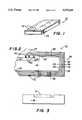
- FIG. 1is a perspective view of an electronic package of the present invention
- FIG. 2is a cross-sectional view of the electronic package of FIG. 1;
- FIG. 3is a side view of an integrated circuit mounted to a substrate
- FIG. 4is a view similar to FIG. 3 showing a pair of flexible circuits attached to the integrated circuit and bonded to a top surface of the substrate;
- FIG. 5is a view similar to FIG. 4, showing the flexible circuits wrapped around the substrate;
- FIG. 6is a view similar to FIG. 5, showing a plurality of solder preforms that are then reflowed into metal pads in the flexible circuits.
- FIG. 1shows an electronic package assembly 10 of the present invention.
- the assembly 10has a plurality of pads 12 that can be soldered to a printed circuit board (not shown).
- the circuit boardtypically contains a number of assemblies 10 that communicate through the board.
- the pads 12are preferably arranged in a grid like pattern to maximize the pin density of the package 10.
- the package 10includes an electrical device 14 which is typically an integrated circuit (IC) that contains logic, memory, etc., as is known in the art.
- the device 14is mounted to a substrate 16 and located within a cavity 18 formed in the top surface 20 of the substrate 16.
- the substrate 16also has a bottom surface 22 and a pair of side surfaces 24.
- the package 10includes a flexible circuit 26 that wraps around the substrate 16.
- the flexible circuit 26may include a first layer of dielectric material 28 that separates the substrate 16 from a layer of conductive signal lines 30.
- the dielectric materialis preferably constructed from a polyimide that is flexible enough to bend around the substrate 16.
- the conductive signal lines 30are typically copper lines etched in a predetermined pattern.
- the flexible circuit 26usually has a plurality of signal lines that transmit digital signals from the IC 14 to the printed circuit board.
- the conductive signal lines 30are typically separated from an outer conductive plane 32 by a second layer of dielectric 34.
- the conductive plane 32can be used as either a power or ground plane for the integrated circuit 14.
- the conductive plane 32is preferably covered by an outer layer of dielectric material 36.
- the flexible circuit 26may have additional layers of signal lines and power/ground planes separated by layers of dielectric.
- the flexible circuit 26may also include vias 38 that interconnect the different conductive signal lines and/or the conductive planes.
- the signal lines 30may be constructed so that no two signal lines run parallel along the entire length of the flexible circuit 26. Such a construction reduces the inductance and capacitance of the circuit and the amount of electrical noise between the lines. Controlling the impedance of the circuit 26 is particularly important for high speed chips 14.
- the flexible circuit 26has a plurality of leads 40 that extend from the signal lines 30 and power plane 32.
- the leads 40are bonded to pads 42 on the surface of the device 14. Both the device 14 and the cavity 18 are covered with a dielectric material 44.
- the dielectric material 44is preferably a plastic typically used to encapsulate electrical devices.
- the pads 12extend from the signal lines 30 and power/ground plane 32.
- the pads 12couple the device 14 to the printed circuit board through the signal lines 30 and power/ground plane 32 of the flexible circuit 26.
- the substrate 16is preferably constructed from a metal such as copper which is both electrically and thermally conductive.
- the substrate 16may also function as a power/ground plane, wherein a plurality of pads 12 are coupled to the substrate 16.
- the power/ground pads 12also provide a thermal path for heat to flow from the substrate 16 to the circuit board.
- the high thermal conductivity of the copper substrate 16greatly reduces the temperature differential throughout the package 10 and the junction temperatures of the discrete elements on the device 14.
- the power/ground pads and signal padsboth extend through holes 46 formed in the power/ground plane 32 and dielectric layers.
- the holes 46typically contain a dielectric material between the power/ground plane 32 and the pads 12 to prevent shorting between the two conductive members.
- FIGS. 3-6show a preferred method of constructing the package assembly 10 of the present invention.
- the substrate 16is covered with a layer of polyimide 28 that has a layer of adhesive on both sides of the dielectric material 28.
- the polyimide 28covers the areas of the substrate 16 that will be adjacent to the signal lines 30 and conductive plane 32 of the flexible circuit 26. If the substrate 16 is to be used as a power/ground plane, via holes 46 can be drilled, punched or etched into the polyimide 28 before the dielectric is attached to the substrate 16.
- the device 14is mounted to the cavity 18 of the substrate 16 by techniques known in the art.
- a single flexible circuit 26 containing the signal lines 30 and conductive plane 32can then be wrapped around the substrate 16, so that the leads 40 of the circuit 26 are aligned with the surface pads of the device 14.
- the circuit 26can then be bonded to the substrate.16 in an autoclave which applies heat and pressure to the adhesive of the polyimide 28.
- the leads 40 of the circuit 26are wire bonded to the pads of the device 14.
- the package 10may utilize two separate flexible circuits 26 that are initially wire bonded to the device 14 before the circuit 26 are attached to the substrate 16. The wire bonding step of this method may occur before or after the device 14 is mounted to the substrate 16 .
- the flexible circuit 26is typically tested before the circuit 26 is bonded to the substrate 16.
- the substrate 16may include alignment means such as a pin (s) that aligns the flexible circuit 26 with the substrate 16, so that the leads 40 and pads 12 are assembled in the proper locations.
- the flexible circuit 26can be attached to the top surface 20 of the substrate before the circuit 26 is bonded to the device 14, so that the leads 40 remain essentially parallel with the top surface of the device during the wire bonding process. After the device 14 and flexible circuit 26 are attached to the substrate 16, the device 14 is encapsulated with the dielectric material 44.
- the pads 12can be formed by placing a solder preform 48 into each hole 46 of the circuit 26. The package is then heated to reflow the solder, so that the solder attaches to the corresponding conductive members 16, 30 or 32.
- the solder preforms 48can be placed into the holes with a simple vacuum controlled tooling fixture (not shown).
- the pads 12are shown and described as being formed after the flexible circuit 26 is assembled to the substrate 16, it is to be understood that the pads 12 could be created during the manufacturing process of the circuit 26.
- the assembly 10is typically constructed so that the pads 12 are located throughout the entire bottom surface 22 of the substrate 16, thereby maximizing the pin density of the package 10.
Landscapes
- Engineering & Computer Science (AREA)
- Computer Hardware Design (AREA)
- Microelectronics & Electronic Packaging (AREA)
- Power Engineering (AREA)
- Physics & Mathematics (AREA)
- Condensed Matter Physics & Semiconductors (AREA)
- General Physics & Mathematics (AREA)
- Structure Of Printed Boards (AREA)
Abstract
Description
1. Field of the Invention
The present invention relates to an electronic package assembly.
2. Description of Related Art
Electronic packages typically include an integrated circuit that is encapsulated in a plastic or ceramic housing. The housing has a plurality of wire leads or pads that are coupled to the circuit. The package is typically mounted to a printed circuit board by soldering the leads/pads to corresponding pads or plated through holes in the board.
Integrated circuits generate heat which flows into the housing. The heat is removed from the package primarily by convection from the housing, or conduction into the circuit board through the leads/pads. Plastic and ceramic are relatively poor thermal conductors, wherein the heat can create high junction temperatures in the circuit. It is therefore desirable to provide an electronic package assembly that is thermally efficient in removing heat generated by an internal electrical device.
Electronic packages are typically constructed with internal signal lines that are parallel with each other. When used with a high speed circuit, parallel lines can produce cross-talk and other electrical noise in the signals. It is therefore desirable to have an electronic package that minimizes the amount of electrical noise in a signal that travels through the package. Additionally, it is also desirable to have an electronic package assembly which maximizes the lead density of the package and the input/output (I/O) of the integrated circuit.
The present invention is an electronic package assembly that includes a flexible circuit wrapped around a metal substrate. The leads of the flexible circuit are connected to an integrated circuit that is mounted to the top surface of the substrate. The flexible circuit has a plurality of metal pads located adjacent to the bottom surface of the substrate. The flexible circuit also contains a power/ground plane and a number of conductive signal lines that couple the integrated circuit to the metal pads. The metal pads are typically soldered to a printed circuit board, so that the integrated circuit is coupled to the board.
The flexible circuit may have multiple layers of signal lines that are interconnected to reduce the amount parallelism and cross-talk between the lines. The substrate is typically constructed from a metal such as copper which reduces the overall thermal resistance of the package. The assembly may also be construed so that the substrate functions as a power/ground plane. The metal pads typically would fully populate the bottom surface of the substrate, so that the package has a maximum number of contacts.
Therefore it is an object of the present invention to provide an electronic package assembly that is thermally efficient in removing heat from an integrated circuit.
It is also an object of the present invention to provide an electronic package assembly that reduces the amount of electrical noise in the signal lines of the package.
It is also an object of the present invention to provide an electronic package assembly that utilizes an optimum amount of leads.
The objects and advantages of the present invention will become more readily apparent to those ordinarily skilled in the art after reviewing the following detailed description and accompanying drawings, wherein:
FIG. 1 is a perspective view of an electronic package of the present invention;
FIG. 2 is a cross-sectional view of the electronic package of FIG. 1;
FIG. 3 is a side view of an integrated circuit mounted to a substrate;
FIG. 4 is a view similar to FIG. 3 showing a pair of flexible circuits attached to the integrated circuit and bonded to a top surface of the substrate;
FIG. 5 is a view similar to FIG. 4, showing the flexible circuits wrapped around the substrate;
FIG. 6 is a view similar to FIG. 5, showing a plurality of solder preforms that are then reflowed into metal pads in the flexible circuits.
Referring to the drawings more particularly reference numbers, FIG. 1 shows anelectronic package assembly 10 of the present invention. Theassembly 10 has a plurality ofpads 12 that can be soldered to a printed circuit board (not shown). The circuit board typically contains a number ofassemblies 10 that communicate through the board. Thepads 12 are preferably arranged in a grid like pattern to maximize the pin density of thepackage 10.
As shown in FIG. 2, thepackage 10 includes anelectrical device 14 which is typically an integrated circuit (IC) that contains logic, memory, etc., as is known in the art. Thedevice 14 is mounted to asubstrate 16 and located within acavity 18 formed in thetop surface 20 of thesubstrate 16. Thesubstrate 16 also has abottom surface 22 and a pair ofside surfaces 24.
Thepackage 10 includes aflexible circuit 26 that wraps around thesubstrate 16. Theflexible circuit 26 may include a first layer ofdielectric material 28 that separates thesubstrate 16 from a layer ofconductive signal lines 30. The dielectric material is preferably constructed from a polyimide that is flexible enough to bend around thesubstrate 16. Theconductive signal lines 30 are typically copper lines etched in a predetermined pattern. Theflexible circuit 26 usually has a plurality of signal lines that transmit digital signals from theIC 14 to the printed circuit board.
Theconductive signal lines 30 are typically separated from an outerconductive plane 32 by a second layer of dielectric 34. Theconductive plane 32 can be used as either a power or ground plane for the integratedcircuit 14. Theconductive plane 32 is preferably covered by an outer layer ofdielectric material 36, Theflexible circuit 26 may have additional layers of signal lines and power/ground planes separated by layers of dielectric. Theflexible circuit 26 may also includevias 38 that interconnect the different conductive signal lines and/or the conductive planes. Thesignal lines 30 may be constructed so that no two signal lines run parallel along the entire length of theflexible circuit 26. Such a construction reduces the inductance and capacitance of the circuit and the amount of electrical noise between the lines. Controlling the impedance of thecircuit 26 is particularly important forhigh speed chips 14.
The flexible circuit 26has a plurality ofleads 40 that extend from thesignal lines 30 andpower plane 32. Theleads 40 are bonded topads 42 on the surface of thedevice 14. Both thedevice 14 and thecavity 18 are covered with adielectric material 44. Thedielectric material 44 is preferably a plastic typically used to encapsulate electrical devices.
Thepads 12 extend from thesignal lines 30 and power/ground plane 32. Thepads 12 couple thedevice 14 to the printed circuit board through thesignal lines 30 and power/ground plane 32 of theflexible circuit 26. Thesubstrate 16 is preferably constructed from a metal such as copper which is both electrically and thermally conductive. Thesubstrate 16 may also function as a power/ground plane, wherein a plurality ofpads 12 are coupled to thesubstrate 16. The power/ground pads 12 also provide a thermal path for heat to flow from thesubstrate 16 to the circuit board. The high thermal conductivity of thecopper substrate 16 greatly reduces the temperature differential throughout thepackage 10 and the junction temperatures of the discrete elements on thedevice 14. The power/ground pads and signal pads both extend throughholes 46 formed in the power/ground plane 32 and dielectric layers. Theholes 46 typically contain a dielectric material between the power/ground plane 32 and thepads 12 to prevent shorting between the two conductive members.
FIGS. 3-6 show a preferred method of constructing thepackage assembly 10 of the present invention. Thesubstrate 16 is covered with a layer ofpolyimide 28 that has a layer of adhesive on both sides of thedielectric material 28. Thepolyimide 28 covers the areas of thesubstrate 16 that will be adjacent to thesignal lines 30 andconductive plane 32 of theflexible circuit 26. If thesubstrate 16 is to be used as a power/ground plane, viaholes 46 can be drilled, punched or etched into thepolyimide 28 before the dielectric is attached to thesubstrate 16.
Thedevice 14 is mounted to thecavity 18 of thesubstrate 16 by techniques known in the art. A singleflexible circuit 26 containing thesignal lines 30 andconductive plane 32 can then be wrapped around thesubstrate 16, so that the leads 40 of thecircuit 26 are aligned with the surface pads of thedevice 14. Thecircuit 26 can then be bonded to the substrate.16 in an autoclave which applies heat and pressure to the adhesive of thepolyimide 28. The leads 40 of thecircuit 26 are wire bonded to the pads of thedevice 14. As an alternate method, thepackage 10 may utilize two separateflexible circuits 26 that are initially wire bonded to thedevice 14 before thecircuit 26 are attached to thesubstrate 16. The wire bonding step of this method may occur before or after thedevice 14 is mounted to thesubstrate 16 . Theflexible circuit 26 is typically tested before thecircuit 26 is bonded to thesubstrate 16.
Thesubstrate 16 may include alignment means such as a pin (s) that aligns theflexible circuit 26 with thesubstrate 16, so that theleads 40 andpads 12 are assembled in the proper locations. Theflexible circuit 26 can be attached to thetop surface 20 of the substrate before thecircuit 26 is bonded to thedevice 14, so that theleads 40 remain essentially parallel with the top surface of the device during the wire bonding process. After thedevice 14 andflexible circuit 26 are attached to thesubstrate 16, thedevice 14 is encapsulated with thedielectric material 44.
After theflexible circuit 26 is bonded to thesubstrate 16, thepads 12 can be formed by placing asolder preform 48 into eachhole 46 of thecircuit 26. The package is then heated to reflow the solder, so that the solder attaches to the correspondingconductive members pads 12 are shown and described as being formed after theflexible circuit 26 is assembled to thesubstrate 16, it is to be understood that thepads 12 could be created during the manufacturing process of thecircuit 26. Theassembly 10 is typically constructed so that thepads 12 are located throughout theentire bottom surface 22 of thesubstrate 16, thereby maximizing the pin density of thepackage 10.
While certain exemplary embodiments have been described and shown in the accompanying drawings, it is to be understood that such embodiments are merely illustrative of and not restrictive on the broad invention, and that this invention not be limited to the specific constructions and arrangements shown and described, since various other modifications may occur to those ordinarily skilled in the art.
Claims (10)
1. An electronic assembly, comprising:
a metal substrate having a top surface, a bottom surface and a cavity in said top surface;
an electrical device mounted into said cavity of said substrate; and,
a flexible circuit wrapped around said substrate, said flexible circuit having a first layer of dielectric that separates said substrate from a plurality of first signal lines and a second layer of dielectric that separates said first signal lines from a power/ground plane, said first signal lines and said power/ground plane being coupled to said electrical device, said flexible circuit having a plurality of metal pads located adjacent to said bottom surface of said substrate and coupled to said first signal lines and said power/ground plane.
2. The assembly as recited in claim 1, wherein at least one of said metal pads is coupled to said metal substrate.
3. The assembly as recited in claim 1, wherein said flexible circuit includes a plurality of second signal lines separated from said first signal lines by a layer of dielectric, said flexible circuit having a plurality of vias that couple said first signal lines to said second signal lines.
4. The assembly as recited in claim 1, further comprising a dielectric material that encapsulates said electrical device.
5. The assembly as recited in claim 1, wherein said flexible circuit has an outer layer of dielectric that covers said power/ground plane.
6. An electronic assembly, comprising:
a metal substrate having a top surface, a bottom surface and a cavity in said top surface;
an electrical device mounted into said cavity of said substrate; and,
a flexible circuit wrapped around said substrate, said flexible circuit having a first layer of dielectric that separates said substrate from a power/ground plane and a second layer of dielectric that separates said power/ground plane from a plurality of first signal lines, said first signal lines and said power/ground plane being coupled to said electrical device, said flexible circuit having a plurality of metal pads located adjacent to said bottom surface of said substrate and coupled to said first signal lines and said power/ground plane.
7. The assembly as recited in claim 6, wherein at least one of said metal pads is coupled to said metal substrate.
8. The assembly as recited in claim 7, wherein said flexible circuit includes a plurality of second signal lines separated from said first signal lines by a layer of dielectric, said flexible circuit having a plurality of vias that couple said first signal lines to said second signal lines.
9. The assembly as recited in claim 8, further comprising a dielectric material that encapsulates said electrical device.
10. The assembly as recited in claim 6, wherein said flexible circuit has an outer layer of dielectric that covers said plurality of first signal lines.
Priority Applications (2)
| Application Number | Priority Date | Filing Date | Title |
|---|---|---|---|
| US07/985,175US5375041A (en) | 1992-12-02 | 1992-12-02 | Ra-tab array bump tab tape based I.C. package |
| US08/228,095US5362656A (en) | 1992-12-02 | 1994-04-15 | Method of making an electronic assembly having a flexible circuit wrapped around a substrate |
Applications Claiming Priority (1)
| Application Number | Priority Date | Filing Date | Title |
|---|---|---|---|
| US07/985,175US5375041A (en) | 1992-12-02 | 1992-12-02 | Ra-tab array bump tab tape based I.C. package |
Related Child Applications (1)
| Application Number | Title | Priority Date | Filing Date |
|---|---|---|---|
| US08/228,095DivisionUS5362656A (en) | 1992-12-02 | 1994-04-15 | Method of making an electronic assembly having a flexible circuit wrapped around a substrate |
Publications (1)
| Publication Number | Publication Date |
|---|---|
| US5375041Atrue US5375041A (en) | 1994-12-20 |
Family
ID=25531262
Family Applications (2)
| Application Number | Title | Priority Date | Filing Date |
|---|---|---|---|
| US07/985,175Expired - Fee RelatedUS5375041A (en) | 1992-12-02 | 1992-12-02 | Ra-tab array bump tab tape based I.C. package |
| US08/228,095Expired - Fee RelatedUS5362656A (en) | 1992-12-02 | 1994-04-15 | Method of making an electronic assembly having a flexible circuit wrapped around a substrate |
Family Applications After (1)
| Application Number | Title | Priority Date | Filing Date |
|---|---|---|---|
| US08/228,095Expired - Fee RelatedUS5362656A (en) | 1992-12-02 | 1994-04-15 | Method of making an electronic assembly having a flexible circuit wrapped around a substrate |
Country Status (1)
| Country | Link |
|---|---|
| US (2) | US5375041A (en) |
Cited By (81)
| Publication number | Priority date | Publication date | Assignee | Title |
|---|---|---|---|---|
| US5621242A (en)* | 1994-05-16 | 1997-04-15 | Samsung Electronics Co., Ltd. | Semiconductor package having support film formed on inner leads |
| US5757998A (en)* | 1996-10-02 | 1998-05-26 | International Business Machines Corporation | Multigigabit adaptable transceiver module |
| EP0847088A3 (en)* | 1996-12-03 | 1998-12-09 | Oki Electric Industry Co., Ltd. | Semiconductor device, method for manufacturing the same, and method for mounting the same |
| US5876215A (en)* | 1995-07-07 | 1999-03-02 | Minnesota Mining And Manufacturing Company | Separable electrical connector assembly having a planar array of conductive protrusions |
| US5952717A (en)* | 1994-12-29 | 1999-09-14 | Sony Corporation | Semiconductor device and method for producing the same |
| US6167948B1 (en) | 1996-11-18 | 2001-01-02 | Novel Concepts, Inc. | Thin, planar heat spreader |
| US6172423B1 (en)* | 1997-11-15 | 2001-01-09 | Hyundai Electronics Industries Co., Ltd. | Layer-type ball grid array semiconductor package and fabrication method thereof |
| US6173489B1 (en) | 1996-09-26 | 2001-01-16 | Intel Corporation | Organic substrate (PCB) slip plane “stress deflector” for flip chip devices |
| US6198160B1 (en)* | 1997-02-12 | 2001-03-06 | Oki Electric Industry Co., Ltd. | Surface mounted type semiconductor device with wrap-around external leads |
| US6262895B1 (en)* | 2000-01-13 | 2001-07-17 | John A. Forthun | Stackable chip package with flex carrier |
| US6369331B1 (en)* | 1999-09-01 | 2002-04-09 | Fujitsu Limited | Printed circuit board for semiconductor package and method of making same |
| US6376769B1 (en) | 1999-05-18 | 2002-04-23 | Amerasia International Technology, Inc. | High-density electronic package, and method for making same |
| US6410857B1 (en) | 2001-03-01 | 2002-06-25 | Lockheed Martin Corporation | Signal cross-over interconnect for a double-sided circuit card assembly |
| US6441475B2 (en)* | 1999-09-13 | 2002-08-27 | Vishay Intertechnology, Inc. | Chip scale surface mount package for semiconductor device and process of fabricating the same |
| US6465745B1 (en)* | 2000-06-28 | 2002-10-15 | Advanced Micro Devices, Inc. | Micro-BGA beam lead connection |
| US20020190367A1 (en)* | 2001-06-15 | 2002-12-19 | Mantz Frank E. | Slice interconnect structure |
| US20030002267A1 (en)* | 2001-06-15 | 2003-01-02 | Mantz Frank E. | I/O interface structure |
| US6528353B2 (en)* | 1998-10-21 | 2003-03-04 | Hyundai Electronics Industries Co., Ltd. | Chip stack-type semiconductor package and method for fabricating the same |
| US20030051911A1 (en)* | 2001-09-20 | 2003-03-20 | Roeters Glen E. | Post in ring interconnect using 3-D stacking |
| US20030057544A1 (en)* | 2001-09-13 | 2003-03-27 | Nathan Richard J. | Integrated assembly protocol |
| US20030059976A1 (en)* | 2001-09-24 | 2003-03-27 | Nathan Richard J. | Integrated package and methods for making same |
| US20030085452A1 (en)* | 2001-11-05 | 2003-05-08 | International Business Machines Corporation | Packaging architecture for a multiple array transceiver using a continuous flexible circuit |
| US6573461B2 (en) | 2001-09-20 | 2003-06-03 | Dpac Technologies Corp | Retaining ring interconnect used for 3-D stacking |
| US6576992B1 (en) | 2001-10-26 | 2003-06-10 | Staktek Group L.P. | Chip scale stacking system and method |
| US6580031B2 (en) | 2000-03-14 | 2003-06-17 | Amerasia International Technology, Inc. | Method for making a flexible circuit interposer having high-aspect ratio conductors |
| US20030153119A1 (en)* | 2002-02-14 | 2003-08-14 | Nathan Richard J. | Integrated circuit package and method for fabrication |
| US6642612B2 (en)* | 1999-12-29 | 2003-11-04 | Advanced Semiconductor Engineering, Inc. | Lead-bond type chip package and manufacturing method thereof |
| US6660561B2 (en)* | 2000-06-15 | 2003-12-09 | Dpac Technologies Corp. | Method of assembling a stackable integrated circuit chip |
| US20040108584A1 (en)* | 2002-12-05 | 2004-06-10 | Roeters Glen E. | Thin scale outline package |
| US20040159462A1 (en)* | 1999-06-01 | 2004-08-19 | Chung Kevin Kwong-Tai | Flexible dielectric electronic substrate and method for making same |
| US20040183183A1 (en)* | 2001-10-26 | 2004-09-23 | Staktek Group, L.P. | Integrated circuit stacking system and method |
| US20040191442A1 (en)* | 2003-03-27 | 2004-09-30 | Florencia Lim | Surface modification of expanded ultra high molecular weight polyethylene (eUHMWPE) for improved bondability |
| US20040207990A1 (en)* | 2003-04-21 | 2004-10-21 | Rose Andrew C. | Stair-step signal routing |
| US6814588B1 (en)* | 2001-12-05 | 2004-11-09 | Adaptec, Inc. | Overmold cable terminator |
| US20040227222A1 (en)* | 2003-02-28 | 2004-11-18 | Elpida Memory, Inc | Stacked semiconductor package |
| US20050094382A1 (en)* | 2003-10-31 | 2005-05-05 | Noah Lassar | Connection pad layouts |
| US6903458B1 (en) | 2002-06-20 | 2005-06-07 | Richard J. Nathan | Embedded carrier for an integrated circuit chip |
| US6914324B2 (en) | 2001-10-26 | 2005-07-05 | Staktek Group L.P. | Memory expansion and chip scale stacking system and method |
| US6940729B2 (en) | 2001-10-26 | 2005-09-06 | Staktek Group L.P. | Integrated circuit stacking system and method |
| US7026708B2 (en) | 2001-10-26 | 2006-04-11 | Staktek Group L.P. | Low profile chip scale stacking system and method |
| US7033861B1 (en) | 2005-05-18 | 2006-04-25 | Staktek Group L.P. | Stacked module systems and method |
| US7053478B2 (en) | 2001-10-26 | 2006-05-30 | Staktek Group L.P. | Pitch change and chip scale stacking system |
| US7081373B2 (en) | 2001-12-14 | 2006-07-25 | Staktek Group, L.P. | CSP chip stack with flex circuit |
| US7154171B1 (en)* | 2002-02-22 | 2006-12-26 | Amkor Technology, Inc. | Stacking structure for semiconductor devices using a folded over flexible substrate and method therefor |
| US7180167B2 (en) | 2001-10-26 | 2007-02-20 | Staktek Group L. P. | Low profile stacking system and method |
| US7202555B2 (en) | 2001-10-26 | 2007-04-10 | Staktek Group L.P. | Pitch change and chip scale stacking system and method |
| USRE39628E1 (en) | 1999-05-05 | 2007-05-15 | Stakick Group, L.P. | Stackable flex circuit IC package and method of making same |
| US20070111567A1 (en)* | 2003-11-03 | 2007-05-17 | Commissariat A L'energie Atomique | Method and device for connecting chips |
| US7289327B2 (en) | 2006-02-27 | 2007-10-30 | Stakick Group L.P. | Active cooling methods and apparatus for modules |
| US7304382B2 (en) | 2006-01-11 | 2007-12-04 | Staktek Group L.P. | Managed memory component |
| US7310458B2 (en) | 2001-10-26 | 2007-12-18 | Staktek Group L.P. | Stacked module systems and methods |
| US7309914B2 (en) | 2005-01-20 | 2007-12-18 | Staktek Group L.P. | Inverted CSP stacking system and method |
| US7324352B2 (en) | 2004-09-03 | 2008-01-29 | Staktek Group L.P. | High capacity thin module system and method |
| US7371609B2 (en) | 2001-10-26 | 2008-05-13 | Staktek Group L.P. | Stacked module systems and methods |
| US7417310B2 (en) | 2006-11-02 | 2008-08-26 | Entorian Technologies, Lp | Circuit module having force resistant construction |
| US7423885B2 (en) | 2004-09-03 | 2008-09-09 | Entorian Technologies, Lp | Die module system |
| US7443023B2 (en) | 2004-09-03 | 2008-10-28 | Entorian Technologies, Lp | High capacity thin module system |
| US7446410B2 (en) | 2004-09-03 | 2008-11-04 | Entorian Technologies, Lp | Circuit module with thermal casing systems |
| US7468553B2 (en) | 2006-10-20 | 2008-12-23 | Entorian Technologies, Lp | Stackable micropackages and stacked modules |
| US7468893B2 (en) | 2004-09-03 | 2008-12-23 | Entorian Technologies, Lp | Thin module system and method |
| US7480152B2 (en) | 2004-09-03 | 2009-01-20 | Entorian Technologies, Lp | Thin module system and method |
| US7485951B2 (en) | 2001-10-26 | 2009-02-03 | Entorian Technologies, Lp | Modularized die stacking system and method |
| US7508069B2 (en) | 2006-01-11 | 2009-03-24 | Entorian Technologies, Lp | Managed memory component |
| US7508058B2 (en) | 2006-01-11 | 2009-03-24 | Entorian Technologies, Lp | Stacked integrated circuit module |
| US7511968B2 (en) | 2004-09-03 | 2009-03-31 | Entorian Technologies, Lp | Buffered thin module system and method |
| US7511969B2 (en) | 2006-02-02 | 2009-03-31 | Entorian Technologies, Lp | Composite core circuit module system and method |
| US7522421B2 (en) | 2004-09-03 | 2009-04-21 | Entorian Technologies, Lp | Split core circuit module |
| US7542304B2 (en) | 2003-09-15 | 2009-06-02 | Entorian Technologies, Lp | Memory expansion and integrated circuit stacking system and method |
| US7542297B2 (en) | 2004-09-03 | 2009-06-02 | Entorian Technologies, Lp | Optimized mounting area circuit module system and method |
| US7576995B2 (en) | 2005-11-04 | 2009-08-18 | Entorian Technologies, Lp | Flex circuit apparatus and method for adding capacitance while conserving circuit board surface area |
| US7579687B2 (en) | 2004-09-03 | 2009-08-25 | Entorian Technologies, Lp | Circuit module turbulence enhancement systems and methods |
| US7606050B2 (en) | 2004-09-03 | 2009-10-20 | Entorian Technologies, Lp | Compact module system and method |
| US7606040B2 (en) | 2004-09-03 | 2009-10-20 | Entorian Technologies, Lp | Memory module system and method |
| US7606049B2 (en) | 2004-09-03 | 2009-10-20 | Entorian Technologies, Lp | Module thermal management system and method |
| US7605454B2 (en) | 2006-01-11 | 2009-10-20 | Entorian Technologies, Lp | Memory card and method for devising |
| US7608920B2 (en) | 2006-01-11 | 2009-10-27 | Entorian Technologies, Lp | Memory card and method for devising |
| US7616452B2 (en) | 2004-09-03 | 2009-11-10 | Entorian Technologies, Lp | Flex circuit constructions for high capacity circuit module systems and methods |
| US7656678B2 (en) | 2001-10-26 | 2010-02-02 | Entorian Technologies, Lp | Stacked module systems |
| US7719098B2 (en) | 2001-10-26 | 2010-05-18 | Entorian Technologies Lp | Stacked modules and method |
| US7760513B2 (en) | 2004-09-03 | 2010-07-20 | Entorian Technologies Lp | Modified core for circuit module system and method |
| JP2019145763A (en)* | 2018-02-19 | 2019-08-29 | サムソン エレクトロ−メカニックス カンパニーリミテッド. | Printed circuit board and electronic device including the same |
Families Citing this family (38)
| Publication number | Priority date | Publication date | Assignee | Title |
|---|---|---|---|---|
| US5854534A (en) | 1992-08-05 | 1998-12-29 | Fujitsu Limited | Controlled impedence interposer substrate |
| US5399902A (en)* | 1993-03-04 | 1995-03-21 | International Business Machines Corporation | Semiconductor chip packaging structure including a ground plane |
| US5831828A (en)* | 1993-06-03 | 1998-11-03 | International Business Machines Corporation | Flexible circuit board and common heat spreader assembly |
| GB2288286A (en)* | 1994-03-30 | 1995-10-11 | Plessey Semiconductors Ltd | Ball grid array arrangement |
| DE69527473T2 (en)* | 1994-05-09 | 2003-03-20 | Nec Corp., Tokio/Tokyo | Semiconductor arrangement consisting of a semiconductor chip, which is connected by means of contact bumps on the printed circuit board, and assembly method |
| US5482897A (en)* | 1994-07-19 | 1996-01-09 | Lsi Logic Corporation | Integrated circuit with on-chip ground plane |
| US5616958A (en)* | 1995-01-25 | 1997-04-01 | International Business Machines Corporation | Electronic package |
| JP2810647B2 (en)* | 1996-04-30 | 1998-10-15 | 山一電機株式会社 | IC package |
| US6027958A (en)* | 1996-07-11 | 2000-02-22 | Kopin Corporation | Transferred flexible integrated circuit |
| FI962816A7 (en)* | 1996-07-11 | 1998-01-12 | Nokia Corp | Housing structure of microcircuit modules |
| US6881611B1 (en) | 1996-07-12 | 2005-04-19 | Fujitsu Limited | Method and mold for manufacturing semiconductor device, semiconductor device and method for mounting the device |
| KR100242393B1 (en)* | 1996-11-22 | 2000-02-01 | 김영환 | Semiconductor Package and Manufacturing Method |
| US5965848A (en)* | 1997-07-22 | 1999-10-12 | Randice-Lisa Altschul | Disposable portable electronic devices and method of making |
| DE19754874A1 (en) | 1997-12-10 | 1999-06-24 | Siemens Ag | Converting substrate with edge contacts into ball grid array |
| EP0948048A1 (en)* | 1998-03-20 | 1999-10-06 | Caesar Technology Inc. | Chip scale package |
| DE19821857A1 (en) | 1998-05-15 | 1999-11-18 | Biotronik Mess & Therapieg | Highly integrated electronic circuit, especially for use in pacemakers |
| JP3907845B2 (en) | 1998-08-18 | 2007-04-18 | 沖電気工業株式会社 | Semiconductor device |
| US6081026A (en)* | 1998-11-13 | 2000-06-27 | Fujitsu Limited | High density signal interposer with power and ground wrap |
| US6239485B1 (en) | 1998-11-13 | 2001-05-29 | Fujitsu Limited | Reduced cross-talk noise high density signal interposer with power and ground wrap |
| JP2000286549A (en) | 1999-03-24 | 2000-10-13 | Fujitsu Ltd | Method for manufacturing substrate with via connection |
| US6407927B1 (en) | 1999-08-31 | 2002-06-18 | International Business Machines Corporation | Method and structure to increase reliability of input/output connections in electrical devices |
| US6727197B1 (en) | 1999-11-18 | 2004-04-27 | Foster-Miller, Inc. | Wearable transmission device |
| US6392887B1 (en) | 1999-12-14 | 2002-05-21 | Intel Corporation | PLGA-BGA socket using elastomer connectors |
| US6774315B1 (en) | 2000-05-24 | 2004-08-10 | International Business Machines Corporation | Floating interposer |
| ATE494763T1 (en)* | 2000-10-16 | 2011-01-15 | Foster Miller Inc | METHOD FOR PRODUCING A FABRIC ARTICLE WITH ELECTRONIC CIRCUIT AND FABRIC ARTICLE |
| US6486415B2 (en)* | 2001-01-16 | 2002-11-26 | International Business Machines Corporation | Compliant layer for encapsulated columns |
| US20050056921A1 (en)* | 2003-09-15 | 2005-03-17 | Staktek Group L.P. | Stacked module systems and methods |
| US7211884B1 (en) | 2002-01-28 | 2007-05-01 | Pacesetter, Inc. | Implantable medical device construction using a flexible substrate |
| JP2003347741A (en) | 2002-05-30 | 2003-12-05 | Taiyo Yuden Co Ltd | Composite multilayer substrate and module using the same |
| WO2005032447A2 (en) | 2003-08-22 | 2005-04-14 | Foster-Miller, Inc. | Physiological monitoring garment |
| US7223924B2 (en)* | 2003-09-23 | 2007-05-29 | Avago Technologies General Ip (Singapore) Pte. Ltd. | Via placement for layer transitions in flexible circuits with high density ball grid arrays |
| FR2877463B1 (en)* | 2004-11-03 | 2007-01-26 | Gemplus Sa | DEVICE HAVING AN ELECTRONIC MODULE |
| US20080062652A1 (en)* | 2006-09-07 | 2008-03-13 | Wayne Lieberman | Vapor heat spreader |
| TW200945530A (en)* | 2008-04-24 | 2009-11-01 | Chipmos Technologies Inc | Chip package structure |
| US9211085B2 (en) | 2010-05-03 | 2015-12-15 | Foster-Miller, Inc. | Respiration sensing system |
| US9028404B2 (en) | 2010-07-28 | 2015-05-12 | Foster-Miller, Inc. | Physiological status monitoring system |
| US8585606B2 (en) | 2010-09-23 | 2013-11-19 | QinetiQ North America, Inc. | Physiological status monitoring system |
| US20120241876A1 (en)* | 2011-03-25 | 2012-09-27 | Still Charles A | System and method for improving frequency response |
Citations (7)
| Publication number | Priority date | Publication date | Assignee | Title |
|---|---|---|---|---|
| FR2021484A1 (en)* | 1968-10-24 | 1970-07-24 | Inst Halvledarfors | |
| WO1989010005A1 (en)* | 1988-04-12 | 1989-10-19 | Bolger Justin C | Pre-formed chip carrier cavity package |
| US4885126A (en)* | 1986-10-17 | 1989-12-05 | Polonio John D | Interconnection mechanisms for electronic components |
| JPH0448741A (en)* | 1990-06-15 | 1992-02-18 | Matsushita Electric Ind Co Ltd | Semiconductor component mounting body |
| WO1992005582A1 (en)* | 1990-09-24 | 1992-04-02 | Tessera, Inc. | Semiconductor chip assemblies, methods of making same and components for same |
| US5166866A (en)* | 1991-04-03 | 1992-11-24 | Samsung Electronics Co., Ltd. | Semiconductor package |
| US5229916A (en)* | 1992-03-04 | 1993-07-20 | International Business Machines Corporation | Chip edge interconnect overlay element |
Family Cites Families (6)
| Publication number | Priority date | Publication date | Assignee | Title |
|---|---|---|---|---|
| JPS6341054A (en)* | 1986-08-06 | 1988-02-22 | Sanyo Electric Co Ltd | Bonding method of hybrid integrated circuit |
| JPH0239651A (en)* | 1988-07-29 | 1990-02-08 | Nec Corp | Transmission speed converting circuit |
| US4912547A (en)* | 1989-01-30 | 1990-03-27 | International Business Machines Corporation | Tape bonded semiconductor device |
| US5202622A (en)* | 1990-05-24 | 1993-04-13 | Tektronix, Inc. | Adapter and test fixture for an integrated circuit device package |
| US5162265A (en)* | 1990-10-29 | 1992-11-10 | Delco Electronics Corporation | Method of making an electrical interconnection having angular lead design |
| US5278724A (en)* | 1992-07-06 | 1994-01-11 | International Business Machines Corporation | Electronic package and method of making same |
- 1992
- 1992-12-02USUS07/985,175patent/US5375041A/ennot_activeExpired - Fee Related
- 1994
- 1994-04-15USUS08/228,095patent/US5362656A/ennot_activeExpired - Fee Related
Patent Citations (7)
| Publication number | Priority date | Publication date | Assignee | Title |
|---|---|---|---|---|
| FR2021484A1 (en)* | 1968-10-24 | 1970-07-24 | Inst Halvledarfors | |
| US4885126A (en)* | 1986-10-17 | 1989-12-05 | Polonio John D | Interconnection mechanisms for electronic components |
| WO1989010005A1 (en)* | 1988-04-12 | 1989-10-19 | Bolger Justin C | Pre-formed chip carrier cavity package |
| JPH0448741A (en)* | 1990-06-15 | 1992-02-18 | Matsushita Electric Ind Co Ltd | Semiconductor component mounting body |
| WO1992005582A1 (en)* | 1990-09-24 | 1992-04-02 | Tessera, Inc. | Semiconductor chip assemblies, methods of making same and components for same |
| US5166866A (en)* | 1991-04-03 | 1992-11-24 | Samsung Electronics Co., Ltd. | Semiconductor package |
| US5229916A (en)* | 1992-03-04 | 1993-07-20 | International Business Machines Corporation | Chip edge interconnect overlay element |
Non-Patent Citations (6)
| Title |
|---|
| IBM Technical Disclosure Bulletin, "Flexible Leaded Chip Carrier", vol. 29, No. 11, Apr. 1987. |
| IBM Technical Disclosure Bulletin, "Removal of Heat from Direct Chip Attach Circuitry", vol. 32, No. 4A, Sep. 1989. |
| IBM Technical Disclosure Bulletin, Flexible Leaded Chip Carrier , vol. 29, No. 11, Apr. 1987.* |
| IBM Technical Disclosure Bulletin, Removal of Heat from Direct Chip Attach Circuitry , vol. 32, No. 4A, Sep. 1989.* |
| Research Disclosure, "Flexy-Pak--Three Dimensional Memory Package", Mar. 1990, No. 311. |
| Research Disclosure, Flexy Pak Three Dimensional Memory Package , Mar. 1990, No. 311.* |
Cited By (118)
| Publication number | Priority date | Publication date | Assignee | Title |
|---|---|---|---|---|
| US5621242A (en)* | 1994-05-16 | 1997-04-15 | Samsung Electronics Co., Ltd. | Semiconductor package having support film formed on inner leads |
| US5952717A (en)* | 1994-12-29 | 1999-09-14 | Sony Corporation | Semiconductor device and method for producing the same |
| US5876215A (en)* | 1995-07-07 | 1999-03-02 | Minnesota Mining And Manufacturing Company | Separable electrical connector assembly having a planar array of conductive protrusions |
| US6173489B1 (en) | 1996-09-26 | 2001-01-16 | Intel Corporation | Organic substrate (PCB) slip plane “stress deflector” for flip chip devices |
| US5757998A (en)* | 1996-10-02 | 1998-05-26 | International Business Machines Corporation | Multigigabit adaptable transceiver module |
| US6167948B1 (en) | 1996-11-18 | 2001-01-02 | Novel Concepts, Inc. | Thin, planar heat spreader |
| EP1936686A3 (en)* | 1996-12-03 | 2009-03-25 | Oki Electric Industry Co., Ltd. | Semiconductor Device, Method for Manufacturing the same, and Method for Mounting the same |
| US6589817B1 (en) | 1996-12-03 | 2003-07-08 | Oki Electric Industry Co., Ltd. | Semiconductor device, method for manufacturing the same, and method for mounting the same |
| EP0847088A3 (en)* | 1996-12-03 | 1998-12-09 | Oki Electric Industry Co., Ltd. | Semiconductor device, method for manufacturing the same, and method for mounting the same |
| US20090146287A1 (en)* | 1996-12-03 | 2009-06-11 | Oki Electric Industry Co., Ltd. | Semiconductor device having a chip-size package |
| US8154124B2 (en) | 1996-12-03 | 2012-04-10 | Oki Electric Industry Co., Ltd. | Semiconductor device having a chip-size package |
| US6198160B1 (en)* | 1997-02-12 | 2001-03-06 | Oki Electric Industry Co., Ltd. | Surface mounted type semiconductor device with wrap-around external leads |
| US6172423B1 (en)* | 1997-11-15 | 2001-01-09 | Hyundai Electronics Industries Co., Ltd. | Layer-type ball grid array semiconductor package and fabrication method thereof |
| US6528353B2 (en)* | 1998-10-21 | 2003-03-04 | Hyundai Electronics Industries Co., Ltd. | Chip stack-type semiconductor package and method for fabricating the same |
| USRE39628E1 (en) | 1999-05-05 | 2007-05-15 | Stakick Group, L.P. | Stackable flex circuit IC package and method of making same |
| US6376769B1 (en) | 1999-05-18 | 2002-04-23 | Amerasia International Technology, Inc. | High-density electronic package, and method for making same |
| US20040159462A1 (en)* | 1999-06-01 | 2004-08-19 | Chung Kevin Kwong-Tai | Flexible dielectric electronic substrate and method for making same |
| US7154046B2 (en) | 1999-06-01 | 2006-12-26 | Amerasia International Technology, Inc. | Flexible dielectric electronic substrate and method for making same |
| US6369331B1 (en)* | 1999-09-01 | 2002-04-09 | Fujitsu Limited | Printed circuit board for semiconductor package and method of making same |
| US6441475B2 (en)* | 1999-09-13 | 2002-08-27 | Vishay Intertechnology, Inc. | Chip scale surface mount package for semiconductor device and process of fabricating the same |
| US6642612B2 (en)* | 1999-12-29 | 2003-11-04 | Advanced Semiconductor Engineering, Inc. | Lead-bond type chip package and manufacturing method thereof |
| USRE41039E1 (en) | 2000-01-13 | 2009-12-15 | Entorian Technologies, Lp | Stackable chip package with flex carrier |
| US6473308B2 (en) | 2000-01-13 | 2002-10-29 | John A. Forthun | Stackable chip package with flex carrier |
| US6262895B1 (en)* | 2000-01-13 | 2001-07-17 | John A. Forthun | Stackable chip package with flex carrier |
| US6580031B2 (en) | 2000-03-14 | 2003-06-17 | Amerasia International Technology, Inc. | Method for making a flexible circuit interposer having high-aspect ratio conductors |
| US6660561B2 (en)* | 2000-06-15 | 2003-12-09 | Dpac Technologies Corp. | Method of assembling a stackable integrated circuit chip |
| US6465745B1 (en)* | 2000-06-28 | 2002-10-15 | Advanced Micro Devices, Inc. | Micro-BGA beam lead connection |
| US6410857B1 (en) | 2001-03-01 | 2002-06-25 | Lockheed Martin Corporation | Signal cross-over interconnect for a double-sided circuit card assembly |
| US20020190367A1 (en)* | 2001-06-15 | 2002-12-19 | Mantz Frank E. | Slice interconnect structure |
| US20030002267A1 (en)* | 2001-06-15 | 2003-01-02 | Mantz Frank E. | I/O interface structure |
| US20030057544A1 (en)* | 2001-09-13 | 2003-03-27 | Nathan Richard J. | Integrated assembly protocol |
| US6573460B2 (en) | 2001-09-20 | 2003-06-03 | Dpac Technologies Corp | Post in ring interconnect using for 3-D stacking |
| US6573461B2 (en) | 2001-09-20 | 2003-06-03 | Dpac Technologies Corp | Retaining ring interconnect used for 3-D stacking |
| US20030051911A1 (en)* | 2001-09-20 | 2003-03-20 | Roeters Glen E. | Post in ring interconnect using 3-D stacking |
| US20030059976A1 (en)* | 2001-09-24 | 2003-03-27 | Nathan Richard J. | Integrated package and methods for making same |
| US7202555B2 (en) | 2001-10-26 | 2007-04-10 | Staktek Group L.P. | Pitch change and chip scale stacking system and method |
| US7310458B2 (en) | 2001-10-26 | 2007-12-18 | Staktek Group L.P. | Stacked module systems and methods |
| US7495334B2 (en) | 2001-10-26 | 2009-02-24 | Entorian Technologies, Lp | Stacking system and method |
| US7524703B2 (en) | 2001-10-26 | 2009-04-28 | Entorian Technologies, Lp | Integrated circuit stacking system and method |
| US6576992B1 (en) | 2001-10-26 | 2003-06-10 | Staktek Group L.P. | Chip scale stacking system and method |
| US7371609B2 (en) | 2001-10-26 | 2008-05-13 | Staktek Group L.P. | Stacked module systems and methods |
| US6914324B2 (en) | 2001-10-26 | 2005-07-05 | Staktek Group L.P. | Memory expansion and chip scale stacking system and method |
| US6940729B2 (en) | 2001-10-26 | 2005-09-06 | Staktek Group L.P. | Integrated circuit stacking system and method |
| US6955945B2 (en) | 2001-10-26 | 2005-10-18 | Staktek Group L.P. | Memory expansion and chip scale stacking system and method |
| US6956284B2 (en) | 2001-10-26 | 2005-10-18 | Staktek Group L.P. | Integrated circuit stacking system and method |
| US7026708B2 (en) | 2001-10-26 | 2006-04-11 | Staktek Group L.P. | Low profile chip scale stacking system and method |
| US7719098B2 (en) | 2001-10-26 | 2010-05-18 | Entorian Technologies Lp | Stacked modules and method |
| US7053478B2 (en) | 2001-10-26 | 2006-05-30 | Staktek Group L.P. | Pitch change and chip scale stacking system |
| US7335975B2 (en) | 2001-10-26 | 2008-02-26 | Staktek Group L.P. | Integrated circuit stacking system and method |
| US7094632B2 (en) | 2001-10-26 | 2006-08-22 | Staktek Group L.P. | Low profile chip scale stacking system and method |
| US7572671B2 (en) | 2001-10-26 | 2009-08-11 | Entorian Technologies, Lp | Stacked module systems and methods |
| US7586758B2 (en) | 2001-10-26 | 2009-09-08 | Entorian Technologies, Lp | Integrated circuit stacking system |
| US7595550B2 (en) | 2001-10-26 | 2009-09-29 | Entorian Technologies, Lp | Flex-based circuit module |
| US7180167B2 (en) | 2001-10-26 | 2007-02-20 | Staktek Group L. P. | Low profile stacking system and method |
| US7606048B2 (en) | 2001-10-26 | 2009-10-20 | Enthorian Technologies, LP | Integrated circuit stacking system |
| US7485951B2 (en) | 2001-10-26 | 2009-02-03 | Entorian Technologies, Lp | Modularized die stacking system and method |
| US7656678B2 (en) | 2001-10-26 | 2010-02-02 | Entorian Technologies, Lp | Stacked module systems |
| US20040183183A1 (en)* | 2001-10-26 | 2004-09-23 | Staktek Group, L.P. | Integrated circuit stacking system and method |
| US7626273B2 (en) | 2001-10-26 | 2009-12-01 | Entorian Technologies, L.P. | Low profile stacking system and method |
| US7256484B2 (en) | 2001-10-26 | 2007-08-14 | Staktek Group L.P. | Memory expansion and chip scale stacking system and method |
| US20030085452A1 (en)* | 2001-11-05 | 2003-05-08 | International Business Machines Corporation | Packaging architecture for a multiple array transceiver using a continuous flexible circuit |
| US6814588B1 (en)* | 2001-12-05 | 2004-11-09 | Adaptec, Inc. | Overmold cable terminator |
| US7081373B2 (en) | 2001-12-14 | 2006-07-25 | Staktek Group, L.P. | CSP chip stack with flex circuit |
| US7193310B2 (en) | 2001-12-14 | 2007-03-20 | Stuktek Group L.P. | Stacking system and method |
| US20030153119A1 (en)* | 2002-02-14 | 2003-08-14 | Nathan Richard J. | Integrated circuit package and method for fabrication |
| US7154171B1 (en)* | 2002-02-22 | 2006-12-26 | Amkor Technology, Inc. | Stacking structure for semiconductor devices using a folded over flexible substrate and method therefor |
| US6903458B1 (en) | 2002-06-20 | 2005-06-07 | Richard J. Nathan | Embedded carrier for an integrated circuit chip |
| US20040108584A1 (en)* | 2002-12-05 | 2004-06-10 | Roeters Glen E. | Thin scale outline package |
| US6856010B2 (en) | 2002-12-05 | 2005-02-15 | Staktek Group L.P. | Thin scale outline package |
| US20070001299A1 (en)* | 2003-02-28 | 2007-01-04 | Elpida Memory, Inc. | Stacked semiconductor package |
| US7642635B2 (en) | 2003-02-28 | 2010-01-05 | Elpida Memory, Inc. | Stacked semiconductor package |
| US20040227222A1 (en)* | 2003-02-28 | 2004-11-18 | Elpida Memory, Inc | Stacked semiconductor package |
| US20040191442A1 (en)* | 2003-03-27 | 2004-09-30 | Florencia Lim | Surface modification of expanded ultra high molecular weight polyethylene (eUHMWPE) for improved bondability |
| US20040207990A1 (en)* | 2003-04-21 | 2004-10-21 | Rose Andrew C. | Stair-step signal routing |
| US7542304B2 (en) | 2003-09-15 | 2009-06-02 | Entorian Technologies, Lp | Memory expansion and integrated circuit stacking system and method |
| US20050094382A1 (en)* | 2003-10-31 | 2005-05-05 | Noah Lassar | Connection pad layouts |
| US7211736B2 (en)* | 2003-10-31 | 2007-05-01 | Hewlett-Packard Development Company, L.P. | Connection pad layouts |
| US20070169342A1 (en)* | 2003-10-31 | 2007-07-26 | Noah Lassar | Connection pad layouts |
| US7569940B2 (en)* | 2003-11-03 | 2009-08-04 | Commissariat A L'energie Atomique | Method and device for connecting chips |
| US20070111567A1 (en)* | 2003-11-03 | 2007-05-17 | Commissariat A L'energie Atomique | Method and device for connecting chips |
| US7626259B2 (en) | 2004-09-03 | 2009-12-01 | Entorian Technologies, Lp | Heat sink for a high capacity thin module system |
| US7459784B2 (en) | 2004-09-03 | 2008-12-02 | Entorian Technologies, Lp | High capacity thin module system |
| US7511968B2 (en) | 2004-09-03 | 2009-03-31 | Entorian Technologies, Lp | Buffered thin module system and method |
| US7480152B2 (en) | 2004-09-03 | 2009-01-20 | Entorian Technologies, Lp | Thin module system and method |
| US7522425B2 (en) | 2004-09-03 | 2009-04-21 | Entorian Technologies, Lp | High capacity thin module system and method |
| US7522421B2 (en) | 2004-09-03 | 2009-04-21 | Entorian Technologies, Lp | Split core circuit module |
| US7443023B2 (en) | 2004-09-03 | 2008-10-28 | Entorian Technologies, Lp | High capacity thin module system |
| US7423885B2 (en) | 2004-09-03 | 2008-09-09 | Entorian Technologies, Lp | Die module system |
| US7542297B2 (en) | 2004-09-03 | 2009-06-02 | Entorian Technologies, Lp | Optimized mounting area circuit module system and method |
| US7768796B2 (en) | 2004-09-03 | 2010-08-03 | Entorian Technologies L.P. | Die module system |
| US7760513B2 (en) | 2004-09-03 | 2010-07-20 | Entorian Technologies Lp | Modified core for circuit module system and method |
| US7324352B2 (en) | 2004-09-03 | 2008-01-29 | Staktek Group L.P. | High capacity thin module system and method |
| US7737549B2 (en) | 2004-09-03 | 2010-06-15 | Entorian Technologies Lp | Circuit module with thermal casing systems |
| US7579687B2 (en) | 2004-09-03 | 2009-08-25 | Entorian Technologies, Lp | Circuit module turbulence enhancement systems and methods |
| US7446410B2 (en) | 2004-09-03 | 2008-11-04 | Entorian Technologies, Lp | Circuit module with thermal casing systems |
| US7468893B2 (en) | 2004-09-03 | 2008-12-23 | Entorian Technologies, Lp | Thin module system and method |
| US7602613B2 (en) | 2004-09-03 | 2009-10-13 | Entorian Technologies, Lp | Thin module system and method |
| US7606050B2 (en) | 2004-09-03 | 2009-10-20 | Entorian Technologies, Lp | Compact module system and method |
| US7606040B2 (en) | 2004-09-03 | 2009-10-20 | Entorian Technologies, Lp | Memory module system and method |
| US7606042B2 (en) | 2004-09-03 | 2009-10-20 | Entorian Technologies, Lp | High capacity thin module system and method |
| US7606049B2 (en) | 2004-09-03 | 2009-10-20 | Entorian Technologies, Lp | Module thermal management system and method |
| US7616452B2 (en) | 2004-09-03 | 2009-11-10 | Entorian Technologies, Lp | Flex circuit constructions for high capacity circuit module systems and methods |
| US7309914B2 (en) | 2005-01-20 | 2007-12-18 | Staktek Group L.P. | Inverted CSP stacking system and method |
| US7323364B2 (en) | 2005-05-18 | 2008-01-29 | Staktek Group L.P. | Stacked module systems and method |
| US7033861B1 (en) | 2005-05-18 | 2006-04-25 | Staktek Group L.P. | Stacked module systems and method |
| US7576995B2 (en) | 2005-11-04 | 2009-08-18 | Entorian Technologies, Lp | Flex circuit apparatus and method for adding capacitance while conserving circuit board surface area |
| US7508058B2 (en) | 2006-01-11 | 2009-03-24 | Entorian Technologies, Lp | Stacked integrated circuit module |
| US7608920B2 (en) | 2006-01-11 | 2009-10-27 | Entorian Technologies, Lp | Memory card and method for devising |
| US7304382B2 (en) | 2006-01-11 | 2007-12-04 | Staktek Group L.P. | Managed memory component |
| US7605454B2 (en) | 2006-01-11 | 2009-10-20 | Entorian Technologies, Lp | Memory card and method for devising |
| US7508069B2 (en) | 2006-01-11 | 2009-03-24 | Entorian Technologies, Lp | Managed memory component |
| US7511969B2 (en) | 2006-02-02 | 2009-03-31 | Entorian Technologies, Lp | Composite core circuit module system and method |
| US7289327B2 (en) | 2006-02-27 | 2007-10-30 | Stakick Group L.P. | Active cooling methods and apparatus for modules |
| US7468553B2 (en) | 2006-10-20 | 2008-12-23 | Entorian Technologies, Lp | Stackable micropackages and stacked modules |
| US7417310B2 (en) | 2006-11-02 | 2008-08-26 | Entorian Technologies, Lp | Circuit module having force resistant construction |
| US7804985B2 (en) | 2006-11-02 | 2010-09-28 | Entorian Technologies Lp | Circuit module having force resistant construction |
| JP2019145763A (en)* | 2018-02-19 | 2019-08-29 | サムソン エレクトロ−メカニックス カンパニーリミテッド. | Printed circuit board and electronic device including the same |
| JP7119260B2 (en) | 2018-02-19 | 2022-08-17 | サムソン エレクトロ-メカニックス カンパニーリミテッド. | Printed circuit board and electronic equipment with same |
Also Published As
| Publication number | Publication date |
|---|---|
| US5362656A (en) | 1994-11-08 |
Similar Documents
| Publication | Publication Date | Title |
|---|---|---|
| US5375041A (en) | Ra-tab array bump tab tape based I.C. package | |
| US5307240A (en) | Chiplid, multichip semiconductor package design concept | |
| EP0863548B1 (en) | Mounting assembly of integrated circuit device and method for production thereof | |
| KR100611267B1 (en) | High performance, low cost microelectronic circuit package with interposer | |
| US6084777A (en) | Ball grid array package | |
| US5721454A (en) | Integrated circuit package with a plurality of vias that are electrically connected to an internal ground plane and thermally connected to an external heat slug | |
| US6869827B2 (en) | Semiconductor/printed circuit board assembly, and computer system | |
| US5099309A (en) | Three-dimensional memory card structure with internal direct chip attachment | |
| US5102829A (en) | Plastic pin grid array package | |
| US5521435A (en) | Semiconductor device and a fabrication process thereof | |
| US6205654B1 (en) | Method of manufacturing a surface mount package | |
| US6440770B1 (en) | Integrated circuit package | |
| US20010001505A1 (en) | Tape ball grid array with interconnected ground plane | |
| US5625166A (en) | Structure of a thermally and electrically enhanced plastic pin grid array (PPGA) package for high performance devices with wire bond interconnect | |
| JP2004235650A (en) | Stacked chip electronic package having laminate carrier and its producing process | |
| CA2454971A1 (en) | Multi-chip electronic package having laminate carrier and method of making same | |
| WO1997025742A1 (en) | Multi-chip integrated circuit package | |
| JPH0234184B2 (en) | ||
| WO1996013854A9 (en) | Thermally and electrically enhanced plastic pin grid array (ppga) package | |
| US5475565A (en) | Power distribution lid for IC package | |
| US5787575A (en) | Method for plating a bond finger of an intergrated circuit package | |
| US5726860A (en) | Method and apparatus to reduce cavity size and the bondwire length in three tier PGA packages by interdigitating the VCC/VSS | |
| WO1998010466A1 (en) | An integrated circuit package | |
| CA2195038C (en) | Integrated circuit packaging structure | |
| US6747352B1 (en) | Integrated circuit having multiple power/ground connections to a single external terminal |
Legal Events
| Date | Code | Title | Description |
|---|---|---|---|
| AS | Assignment | Owner name:INTEL CORPORATION, CALIFORNIA Free format text:ASSIGNMENT OF ASSIGNORS INTEREST.;ASSIGNOR:MCMAHON, JOHN F.;REEL/FRAME:006346/0037 Effective date:19921125 | |
| CC | Certificate of correction | ||
| FEPP | Fee payment procedure | Free format text:PAYOR NUMBER ASSIGNED (ORIGINAL EVENT CODE: ASPN); ENTITY STATUS OF PATENT OWNER: LARGE ENTITY | |
| FPAY | Fee payment | Year of fee payment:4 | |
| REMI | Maintenance fee reminder mailed | ||
| LAPS | Lapse for failure to pay maintenance fees | ||
| STCH | Information on status: patent discontinuation | Free format text:PATENT EXPIRED DUE TO NONPAYMENT OF MAINTENANCE FEES UNDER 37 CFR 1.362 | |
| FP | Lapsed due to failure to pay maintenance fee | Effective date:20021220 |