US5374582A - Laminated substrate for semiconductor device and manufacturing method thereof - Google Patents
Laminated substrate for semiconductor device and manufacturing method thereofDownload PDFInfo
- Publication number
- US5374582A US5374582AUS08/233,940US23394094AUS5374582AUS 5374582 AUS5374582 AUS 5374582AUS 23394094 AUS23394094 AUS 23394094AUS 5374582 AUS5374582 AUS 5374582A
- Authority
- US
- United States
- Prior art keywords
- region
- substrate
- type
- semiconductor substrate
- main surface
- Prior art date
- Legal status (The legal status is an assumption and is not a legal conclusion. Google has not performed a legal analysis and makes no representation as to the accuracy of the status listed.)
- Expired - Fee Related
Links
Images

Classifications
- H—ELECTRICITY
- H01—ELECTRIC ELEMENTS
- H01L—SEMICONDUCTOR DEVICES NOT COVERED BY CLASS H10
- H01L21/00—Processes or apparatus adapted for the manufacture or treatment of semiconductor or solid state devices or of parts thereof
- H01L21/70—Manufacture or treatment of devices consisting of a plurality of solid state components formed in or on a common substrate or of parts thereof; Manufacture of integrated circuit devices or of parts thereof
- H01L21/71—Manufacture of specific parts of devices defined in group H01L21/70
- H01L21/76—Making of isolation regions between components
- H01L21/762—Dielectric regions, e.g. EPIC dielectric isolation, LOCOS; Trench refilling techniques, SOI technology, use of channel stoppers
- H01L21/7624—Dielectric regions, e.g. EPIC dielectric isolation, LOCOS; Trench refilling techniques, SOI technology, use of channel stoppers using semiconductor on insulator [SOI] technology
- H01L21/76251—Dielectric regions, e.g. EPIC dielectric isolation, LOCOS; Trench refilling techniques, SOI technology, use of channel stoppers using semiconductor on insulator [SOI] technology using bonding techniques
- H—ELECTRICITY
- H01—ELECTRIC ELEMENTS
- H01L—SEMICONDUCTOR DEVICES NOT COVERED BY CLASS H10
- H01L21/00—Processes or apparatus adapted for the manufacture or treatment of semiconductor or solid state devices or of parts thereof
- H01L21/02—Manufacture or treatment of semiconductor devices or of parts thereof
- H01L21/04—Manufacture or treatment of semiconductor devices or of parts thereof the devices having potential barriers, e.g. a PN junction, depletion layer or carrier concentration layer
- H01L21/18—Manufacture or treatment of semiconductor devices or of parts thereof the devices having potential barriers, e.g. a PN junction, depletion layer or carrier concentration layer the devices having semiconductor bodies comprising elements of Group IV of the Periodic Table or AIIIBV compounds with or without impurities, e.g. doping materials
- H01L21/185—Joining of semiconductor bodies for junction formation
- H01L21/187—Joining of semiconductor bodies for junction formation by direct bonding
- H—ELECTRICITY
- H01—ELECTRIC ELEMENTS
- H01L—SEMICONDUCTOR DEVICES NOT COVERED BY CLASS H10
- H01L21/00—Processes or apparatus adapted for the manufacture or treatment of semiconductor or solid state devices or of parts thereof
- H01L21/70—Manufacture or treatment of devices consisting of a plurality of solid state components formed in or on a common substrate or of parts thereof; Manufacture of integrated circuit devices or of parts thereof
- H01L21/71—Manufacture of specific parts of devices defined in group H01L21/70
- H01L21/76—Making of isolation regions between components
- H01L21/761—PN junctions
- Y—GENERAL TAGGING OF NEW TECHNOLOGICAL DEVELOPMENTS; GENERAL TAGGING OF CROSS-SECTIONAL TECHNOLOGIES SPANNING OVER SEVERAL SECTIONS OF THE IPC; TECHNICAL SUBJECTS COVERED BY FORMER USPC CROSS-REFERENCE ART COLLECTIONS [XRACs] AND DIGESTS
- Y10—TECHNICAL SUBJECTS COVERED BY FORMER USPC
- Y10S—TECHNICAL SUBJECTS COVERED BY FORMER USPC CROSS-REFERENCE ART COLLECTIONS [XRACs] AND DIGESTS
- Y10S148/00—Metal treatment
- Y10S148/012—Bonding, e.g. electrostatic for strain gauges
Definitions
- the present inventionrelates to a laminated substrate for semiconductor device and its manufacturing method, and more particularly to a composite substrate for a semiconductor device in which a power device and a control circuit for the power device are integrated, and its manufacturing method.
- a composite dielectrically isolated substrate for monolithically integrates a power device having a current path from the front surface of a substrate to the rear surface and a device, for control circuit for the power device, having current path only on the front surface of the substrate, and its manufacturing method,are disclosed in Japanese Patent Laid Open No. H3-142952.
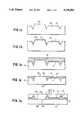
- the method for manufacturing a substrate disclosed in the above mentioned patent specificationis described below by reference to FIGS. 1a a to 1e.
- the methodcomprises the steps of preparing a first semiconductor substrate of a first conductivity type and a second semiconductor substrate of the first conductivity type, forming a first region of a second conductivity type by selectively introducing impurities into one surface of the first semiconductor substrate, forming an epitaxial layer of the first conductivity type on one surface of the second semiconductor substrate, placing said one surface of the first semiconductor substrate and the face of the epitaxial layer in contact with each other and then heating the semiconductor substrates to bond each other, polishing the other surface of the first semiconductor substrate until a predetermined thickness thereof remains, and forming an isolating region of the second conductivity type reaching the buried layer from the polished surface of the first semiconductor substrate polished in the polishing step to form a region of the first conductivity type on the buried layer surrounded by the isolating region.
- FIGS. 1a to 1eare sectional views illustrating in sequence the method for manufacturing a laminated substrate in the prior art
- FIGS. 3a to 3bare sectional views illustrating additional steps to FIG. 2d of the present invention.
- FIG. 4is a sectional view illustrating another embodiment of the present invention.
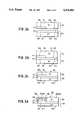
- the second silicon substrate 40is provided by forming an N - type epitaxial layer 42 having a resistivity of about 20 to 80 ⁇ cm and a thickness of about 20 to 50 ⁇ m on the entire surface of an N + type silicon substrate 41 having a resistivity in the range of 0.001 to 0.020 ⁇ cm.
- the surface 43 of the epitaxial layer of the second silicon substrate 40 and one mirror polished surface 34 of the first silicon substrate 30 with the P + type region 32 formed thereinare brought into contact with each other. Then, heat treatment for about two hours at about 1100° C. is carried out to form a composite substrate of the first and second substrates. This process step is well known as wafer direct bonding technique.
- surfaces of the composite substrateare polished both from the exposed surface 44 side and the surface 33 side to predetermined thickness, respectively, and mirror polished surfaces 45 and 35 are formed.
- the N - type portion 38becomes, together with the N - type epitaxial layer 42 and the N + type portion 41 of the silicon substrate 40, a first element formation region in which can be formed a high voltage power element having a current path from an electrode on the surface 35 to an electrode on the surface 45, while the N - type portion 37 surrounded by the P + type isolation region 36 and the P + type buried layer 32 becomes a second element formation region in which can be formed a control circuit element having electrodes only on the surface 35.
- FIGS. 3a to 3ban embodiment for manufacturing an integrated circuit using the laminated substrate for semiconductor device obtained in FIG. 2d will be described.
- a V-shaped isolation groove 51 reaching the buried layer 32is formed in the P + type isolation region 36 by anisotropic wet etching, a silicon dioxide film 52 is formed on the surface of the groove, and the groove is filled by depositing polycrystalline silicon 53 on it.
- the isolation actionbecomes more certain than in the case of the P + type isolation region alone.
- a P type region 61is formed in ring form from the surface 35 of the portion 38 of the silicon substrate 31, a high concentration (low resistivity) N + type source region 62 is formed in ring form in the region 61, a gate electrode 66,(G) is formed on a gate insulating film 65 formed on the region 62 and the portion 38 so as to make the ring like portion of the P type region on the inside of the source region 62 a channel region 64, a source electrode 63,(S) connected to the source region 62 and the P type region 61 is formed, and a drain electrode 67,(D) is formed on the surface 45 of the first silicon substrate 41, thereby constituting a power FET having a current path leading from the source electrode 63 on the surface 35 to the drain electrode 67 on the surface 45.
- the N - type portion 37 isolated by a P-N junctionthere are formed, from the surface 35, high concentration P + type source and drain region 71 and 72, a source electrode 76,(S) and a drain electrode 77,(D) connected to region 71 and 72, respectively, and a gate electrode 75,(G) formed via a gate insulating film 74 on the channel region 73, forming an FET as an element constituting a part of a control circuit.
- FIG. 4is a sectional view of a partial modification of the embodiment in FIGS. 3a to 3b.
- a groove having vertical sidewalls 81 that reach the P + type region 32is formed by anisotropic dry etching, a silicon dioxide film 82 is formed on the sidewalls, and the groove is filled up by depositing polycrystalline silicon 83 on top of it.
- the isolating actionis assured more than in the case of having only the P + type isolation region 36 as in FIG. 3a.
- the first and the second silicon substrates 41 and 31 and the epitaxial layer 42are N (N + or N - ) type, and the isolating region 36 and the buried layer 32 are P (P + ) type, but it is possible to interchange the N type and the P type, and let the first and the second silicon substrates and the epitaxial layer be P (P + or P - ) type, and let the isolating region and the buried layer be N (N + ) type.
- the N type and the P type for the source and drain region, the channel regions, and the likeare naturally to be interchanged.
- single crystal siliconalone needs to be mirror polished in this invention, and it becomes possible to manufacture laminated substrates for semiconductor devices with high productivity, suitable for mass production.
- a silicon dioxide film or a poly crystalline silicon filmis not buried in the single crystal silicon substrate, there will not be generated problems such as a large warping of the substrate or a distortion of single crystal silicon in the element region which may be lead to generation of dislocations in the polishing process or heat treatment process.
- an observation by an optical microscope of etch pit density in a lightly etched surface of the substrate manufactured according to this inventionshowed an improvement of 10 2 pits/cm 2 in contrast to the pit density of about 10 4 pits/cm 2 for the substrate manufactured according to the prior art technique.
- the warp of the substrate manufactured according to this inventionwas reduced to a value of less than 40 ⁇ m in contrast to the value of 50 to 100 ⁇ m for the substrate manufactured according to the prior art technique.
Landscapes
- Engineering & Computer Science (AREA)
- Physics & Mathematics (AREA)
- Condensed Matter Physics & Semiconductors (AREA)
- General Physics & Mathematics (AREA)
- Manufacturing & Machinery (AREA)
- Computer Hardware Design (AREA)
- Microelectronics & Electronic Packaging (AREA)
- Power Engineering (AREA)
- Element Separation (AREA)
Abstract
Description
1. Field of the Invention
The present invention relates to a laminated substrate for semiconductor device and its manufacturing method, and more particularly to a composite substrate for a semiconductor device in which a power device and a control circuit for the power device are integrated, and its manufacturing method.
2. Description of the Prior Art
A composite dielectrically isolated substrate for monolithically integrates a power device having a current path from the front surface of a substrate to the rear surface and a device, for control circuit for the power device, having current path only on the front surface of the substrate, and its manufacturing method, are disclosed in Japanese Patent Laid Open No. H3-142952. The method for manufacturing a substrate disclosed in the above mentioned patent specification is described below by reference to FIGS. 1a a to 1e.
First, as shown in FIG. 1a, a singlecrystal silicon substrate 10 is processed to have athick portion 20 for forming a power device, athin portion 21 for forming a control circuit device and an isolating groove being provided between them. Next, as shown in FIG. 1b, a silicon dioxide film 11 is formed on the entire surface of the rugged surface side of the substrate including the isolating groove. Then, as shown in FIG. 1c, apolycrystalline silicon layer 12 is deposited on the silicon dioxide film 11. In the next step, as shown in FIG. 1d, the substrate is polished until thesingle crystal portion 20 of thesubstrate 10, for forming a power device, is exposed, andmirror surface 22 is formed. Then, as shown in FIG. 1e, themirror surface 22 of thesubstrate 10 and amirror surface 25 of a single crystalsilicon support substrate 13 are brought into contact with and bonded by heat treatment, and thesilicon substrate 10 is polished from theside 23 until the silicon dioxide film 11 is exposed. Thus, a composite dielectrically isolated substrate having adevice formation surface 24 is obtained. It is possible to form a power device having a current path from an electrode formed on thesurface 24 of theportion 20 to a rear surface electrode formed onrear surface 26 of thesupport substrate 13, and it is possible to isolate by the silicon dioxide film 11 the power device from the control circuit device formed on thesurface 24 of theportion 21.
In this conventional technology for composite dielectrically isolated substrate, it is necessary to polish three phases (single crystal silicon, silicon dioxide and polycrystalline silicon) into mirror surfaces on the same plane in order to obtain a bonding surface, but silicon dioxide has a higher hardness compared with single crystal silicon and polycrystalline silicon and it is difficult to uniformly polish them.
Moreover, the polishing process and the bonding process are carried out in a condition in which the silicon dioxide film and the poly crystalline silicon film are embedded in the single crystal silicon substrate. Therefore, a warp of the substrate becomes large in the polishing process and the bonding process which led to the generation of such problems as distortion and dislocation of single crystal of the element region.
It is an object of the present invention to provide a laminated substrate which resolves the above mentioned problems.
The laminated substrate of the present invention comprises a first semiconductor substrate of first conductivity type having a first and a second main surfaces and a second semiconductor substrate having a third and a fourth main surfaces. The first main surface of the first semiconductor substrate is bonded to the third main surface of the second semiconductor substrate. A buried layer of second conductivity type is formed selectively in the first semiconductor substrate. An isolating region of the second conductivity type is formed to reach the buried layer from the second main surface of the first semiconductor substrate to form a region of the first conductivity type on the first region surrounded by the isolating region.
It is another object of the present invention to provide a method for manufacturing the laminated substrate.
The method comprises the steps of preparing a first semiconductor substrate of a first conductivity type and a second semiconductor substrate of the first conductivity type, forming a first region of a second conductivity type by selectively introducing impurities into one surface of the first semiconductor substrate, forming an epitaxial layer of the first conductivity type on one surface of the second semiconductor substrate, placing said one surface of the first semiconductor substrate and the face of the epitaxial layer in contact with each other and then heating the semiconductor substrates to bond each other, polishing the other surface of the first semiconductor substrate until a predetermined thickness thereof remains, and forming an isolating region of the second conductivity type reaching the buried layer from the polished surface of the first semiconductor substrate polished in the polishing step to form a region of the first conductivity type on the buried layer surrounded by the isolating region.
The above and further objects, features and advantages of the present invention will become more apparent from the following detailed description of the embodiments taken in conjunction with the accompanying drawings, wherein:
FIGS. 1a to 1e are sectional views illustrating in sequence the method for manufacturing a laminated substrate in the prior art;
FIGS. 2a to 2d are sectional views illustrating in sequence a method for fabricating a substrate of the present invention;
FIGS. 3a to 3b are sectional views illustrating additional steps to FIG. 2d of the present invention;
FIG. 4 is a sectional view illustrating another embodiment of the present invention.
Referring to the drawings, the present invention will be described in detail as follows.
FIGS. 2a to 2e are sectional views illustrating in sequence a method for fabricating a substrate of the present invention.
First, as shown in FIG. 2a, afirst silicon substrate 30 and asecond silicon substrate 40 are provided. The first silicon substrate is provided by selectively forming a P+ type region 32 having a resistivity of about 0.001 to 0.020 Ω·cm by introducing to high concentration a P type impurity such as boron by means of ion implantation or thermal diffusion from thesurface 34 of an N-type silicon substrate 31 having a resistivity of about 20 to 80 Ω·cm. Thesecond silicon substrate 40 is provided by forming an N- typeepitaxial layer 42 having a resistivity of about 20 to 80 Ω·cm and a thickness of about 20 to 50 μm on the entire surface of an N+type silicon substrate 41 having a resistivity in the range of 0.001 to 0.020 Ω·cm.
Next, as shown in FIG. 2b, thesurface 43 of the epitaxial layer of thesecond silicon substrate 40 and one mirror polishedsurface 34 of thefirst silicon substrate 30 with the P+ type region 32 formed therein are brought into contact with each other. Then, heat treatment for about two hours at about 1100° C. is carried out to form a composite substrate of the first and second substrates. This process step is well known as wafer direct bonding technique.
Then, as shown in FIG. 2c, surfaces of the composite substrate are polished both from the exposedsurface 44 side and thesurface 33 side to predetermined thickness, respectively, and mirror polishedsurfaces
Next, as shown in FIG. 2d, a P+type isolating region 36 having a resistivity in the range of 0.001 to 0.020 Ω·cm reaching the P+ type region 32 is formed by introducing a P type impurity such as boron to high concentration by ion implantation or thermal diffusion from thesurface 35, thereby the N- type portion 37 surrounded by theisolating region 36 on the P+ type region 32 and the remaining N- type portion 38 ofsilicon substrate 31 are electrically isolated by P-N junction.
The N- type portion 38 becomes, together with the N- typeepitaxial layer 42 and the N+ type portion 41 of thesilicon substrate 40, a first element formation region in which can be formed a high voltage power element having a current path from an electrode on thesurface 35 to an electrode on thesurface 45, while the N- type portion 37 surrounded by the P+type isolation region 36 and the P+ type buriedlayer 32 becomes a second element formation region in which can be formed a control circuit element having electrodes only on thesurface 35.
Referring to FIGS. 3a to 3b, an embodiment for manufacturing an integrated circuit using the laminated substrate for semiconductor device obtained in FIG. 2d will be described.
As shown in FIG. 3a, a V-shapedisolation groove 51 reaching the buriedlayer 32 is formed in the P+type isolation region 36 by anisotropic wet etching, asilicon dioxide film 52 is formed on the surface of the groove, and the groove is filled by depositingpolycrystalline silicon 53 on it. With such a structure, the isolation action becomes more certain than in the case of the P+ type isolation region alone.
Next, as shown in FIG. 3b, aP type region 61 is formed in ring form from thesurface 35 of theportion 38 of thesilicon substrate 31, a high concentration (low resistivity) N+type source region 62 is formed in ring form in theregion 61, agate electrode 66,(G) is formed on agate insulating film 65 formed on theregion 62 and theportion 38 so as to make the ring like portion of the P type region on the inside of the source region 62 achannel region 64, asource electrode 63,(S) connected to thesource region 62 and theP type region 61 is formed, and adrain electrode 67,(D) is formed on thesurface 45 of thefirst silicon substrate 41, thereby constituting a power FET having a current path leading from thesource electrode 63 on thesurface 35 to thedrain electrode 67 on thesurface 45. On the other hand, in the N- type portion 37 isolated by a P-N junction there are formed, from thesurface 35, high concentration P+ type source and drainregion source electrode 76,(S) and adrain electrode 77,(D) connected toregion gate electrode 75,(G) formed via agate insulating film 74 on thechannel region 73, forming an FET as an element constituting a part of a control circuit.
FIG. 4 is a sectional view of a partial modification of the embodiment in FIGS. 3a to 3b. In the P+type isolation region 36, a groove havingvertical sidewalls 81 that reach the P+ type region 32 is formed by anisotropic dry etching, asilicon dioxide film 82 is formed on the sidewalls, and the groove is filled up by depositingpolycrystalline silicon 83 on top of it. With such a structure, the isolating action is assured more than in the case of having only the P+type isolation region 36 as in FIG. 3a.
In the above description of the embodiments, it has been assumed that the first and thesecond silicon substrates epitaxial layer 42 are N (N+ or N-) type, and the isolatingregion 36 and the buriedlayer 32 are P (P+) type, but it is possible to interchange the N type and the P type, and let the first and the second silicon substrates and the epitaxial layer be P (P+ or P-) type, and let the isolating region and the buried layer be N (N+) type. In this case, the N type and the P type for the source and drain region, the channel regions, and the like are naturally to be interchanged.
As described in the above, single crystal silicon alone needs to be mirror polished in this invention, and it becomes possible to manufacture laminated substrates for semiconductor devices with high productivity, suitable for mass production. In addition, since a silicon dioxide film or a poly crystalline silicon film is not buried in the single crystal silicon substrate, there will not be generated problems such as a large warping of the substrate or a distortion of single crystal silicon in the element region which may be lead to generation of dislocations in the polishing process or heat treatment process. More specifically, an observation by an optical microscope of etch pit density in a lightly etched surface of the substrate manufactured according to this invention showed an improvement of 102 pits/cm2 in contrast to the pit density of about 104 pits/cm2 for the substrate manufactured according to the prior art technique. Moreover, it was confirmed that the warp of the substrate manufactured according to this invention was reduced to a value of less than 40 μm in contrast to the value of 50 to 100 μm for the substrate manufactured according to the prior art technique.
The invention has thus been shown and described with reference to the specific embodiments. However, it should be noted that the present invention is in no way limited to the details of the embodiments but changes and modification may be made within the scope of the appended claims.
Claims (2)
1. A method for manufacturing a laminated substrate for a semiconductor device comprising the steps of:
(a) preparing a first semiconductor substrate of a first conductivity type and a second semiconductor substrate of the first conductivity type, said first semiconductor substrate having a first main surface and a second main surface opposite to said first main surface and said second semiconductor substrate having a third main surface and a fourth main surface opposite to said third main surface;
(b) forming a first region of a second conductivity type by selectively introducing impurities into said first main surface of said first semiconductor substrate;
(c) forming an epitaxial layer of the first conductivity type on said third main surface of said second semiconductor substrate;
(d) placing said first main surface of the first semiconductor substrate and a surface of said epitaxial layer in contact with each other and then heating said first and second semiconductor substrates to bond each other;
(e) polishing said second main surface of said first semiconductor substrate to produce a polished surface; and
(f) forming an isolating region of the second conductivity type reaching said first region by introducing impurities into said first semiconductor substrate from said polished surface.
2. The method of claim 1, further comprising the steps of forming a groove reaching said buried layer in said isolating region, forming an insulating film on a surface of said groove, and forming polycrystalline silicon on a surface of said insulating film, said insulating film and said polycrystalline silicon cooperating to each other to fill said groove.
Priority Applications (1)
| Application Number | Priority Date | Filing Date | Title |
|---|---|---|---|
| US08/233,940US5374582A (en) | 1994-04-28 | 1994-04-28 | Laminated substrate for semiconductor device and manufacturing method thereof |
Applications Claiming Priority (1)
| Application Number | Priority Date | Filing Date | Title |
|---|---|---|---|
| US08/233,940US5374582A (en) | 1994-04-28 | 1994-04-28 | Laminated substrate for semiconductor device and manufacturing method thereof |
Publications (1)
| Publication Number | Publication Date |
|---|---|
| US5374582Atrue US5374582A (en) | 1994-12-20 |
Family
ID=22879268
Family Applications (1)
| Application Number | Title | Priority Date | Filing Date |
|---|---|---|---|
| US08/233,940Expired - Fee RelatedUS5374582A (en) | 1994-04-28 | 1994-04-28 | Laminated substrate for semiconductor device and manufacturing method thereof |
Country Status (1)
| Country | Link |
|---|---|
| US (1) | US5374582A (en) |
Cited By (9)
| Publication number | Priority date | Publication date | Assignee | Title |
|---|---|---|---|---|
| US5466303A (en)* | 1994-03-25 | 1995-11-14 | Nippondenso Co., Ltd. | Semiconductor device and manufacturing method therefor |
| US5556792A (en)* | 1994-05-19 | 1996-09-17 | Consorzio Per La Ricerca Sulla Microelecttronica Nel Mezzogiorno | Process for manufacturing a power integrated circuit ("PIC") structure with a vertical IGBT |
| US5573972A (en)* | 1994-07-29 | 1996-11-12 | Nec Corporation | Method for manufacturing a silicon bonded wafer |
| US5726089A (en)* | 1992-11-25 | 1998-03-10 | Nec Corporation | Semiconductor device and method for fabricating the same |
| US5943549A (en)* | 1996-12-27 | 1999-08-24 | Komatsu Electronics Metals Co., Ltd. | Method of evaluating silicon wafers |
| US6004406A (en)* | 1994-06-16 | 1999-12-21 | Nec Corporation | Silicon on insulating substrate |
| US6653207B2 (en)* | 2001-03-13 | 2003-11-25 | Mitsubishi Gas Chemical Company, Inc. | Process for the production of electric part |
| EP1617476A3 (en)* | 2004-07-16 | 2007-12-26 | Power Electronics Design Centre | Vertical integration in power integrated circuits |
| US20100108970A1 (en)* | 2008-10-30 | 2010-05-06 | Jun Liu | Memory Devices and Formation Methods |
Citations (8)
| Publication number | Priority date | Publication date | Assignee | Title |
|---|---|---|---|---|
| US4532003A (en)* | 1982-08-09 | 1985-07-30 | Harris Corporation | Method of fabrication bipolar transistor with improved base collector breakdown voltage and collector series resistance |
| JPS61287142A (en)* | 1985-06-13 | 1986-12-17 | Oki Electric Ind Co Ltd | Manufacture of dielectric isolated substrate |
| US4638552A (en)* | 1984-05-09 | 1987-01-27 | Kabushiki Kaisha Toshiba | Method of manufacturing semiconductor substrate |
| US4963505A (en)* | 1987-10-27 | 1990-10-16 | Nippondenso Co., Ltd. | Semiconductor device and method of manufacturing same |
| JPH03142952A (en)* | 1989-10-30 | 1991-06-18 | Nippon Soken Inc | Semiconductor device and its manufacture |
| US5097314A (en)* | 1988-02-08 | 1992-03-17 | Kabushiki Kaisha Toshiba | Dielectrically isolated substrate with isolated high and low breakdown voltage elements |
| US5100814A (en)* | 1989-02-08 | 1992-03-31 | Mitsubishi Denki Kabushiki Kaisha | Semiconductor device and method of manufacturing the same |
| US5234535A (en)* | 1992-12-10 | 1993-08-10 | International Business Machines Corporation | Method of producing a thin silicon-on-insulator layer |
- 1994
- 1994-04-28USUS08/233,940patent/US5374582A/ennot_activeExpired - Fee Related
Patent Citations (8)
| Publication number | Priority date | Publication date | Assignee | Title |
|---|---|---|---|---|
| US4532003A (en)* | 1982-08-09 | 1985-07-30 | Harris Corporation | Method of fabrication bipolar transistor with improved base collector breakdown voltage and collector series resistance |
| US4638552A (en)* | 1984-05-09 | 1987-01-27 | Kabushiki Kaisha Toshiba | Method of manufacturing semiconductor substrate |
| JPS61287142A (en)* | 1985-06-13 | 1986-12-17 | Oki Electric Ind Co Ltd | Manufacture of dielectric isolated substrate |
| US4963505A (en)* | 1987-10-27 | 1990-10-16 | Nippondenso Co., Ltd. | Semiconductor device and method of manufacturing same |
| US5097314A (en)* | 1988-02-08 | 1992-03-17 | Kabushiki Kaisha Toshiba | Dielectrically isolated substrate with isolated high and low breakdown voltage elements |
| US5100814A (en)* | 1989-02-08 | 1992-03-31 | Mitsubishi Denki Kabushiki Kaisha | Semiconductor device and method of manufacturing the same |
| JPH03142952A (en)* | 1989-10-30 | 1991-06-18 | Nippon Soken Inc | Semiconductor device and its manufacture |
| US5234535A (en)* | 1992-12-10 | 1993-08-10 | International Business Machines Corporation | Method of producing a thin silicon-on-insulator layer |
Cited By (16)
| Publication number | Priority date | Publication date | Assignee | Title |
|---|---|---|---|---|
| US5726089A (en)* | 1992-11-25 | 1998-03-10 | Nec Corporation | Semiconductor device and method for fabricating the same |
| US5872388A (en)* | 1992-11-25 | 1999-02-16 | Nec Corporation | Semiconductor device and method for fabricating the same |
| US5466303A (en)* | 1994-03-25 | 1995-11-14 | Nippondenso Co., Ltd. | Semiconductor device and manufacturing method therefor |
| US5556792A (en)* | 1994-05-19 | 1996-09-17 | Consorzio Per La Ricerca Sulla Microelecttronica Nel Mezzogiorno | Process for manufacturing a power integrated circuit ("PIC") structure with a vertical IGBT |
| US6004406A (en)* | 1994-06-16 | 1999-12-21 | Nec Corporation | Silicon on insulating substrate |
| US5573972A (en)* | 1994-07-29 | 1996-11-12 | Nec Corporation | Method for manufacturing a silicon bonded wafer |
| US5943549A (en)* | 1996-12-27 | 1999-08-24 | Komatsu Electronics Metals Co., Ltd. | Method of evaluating silicon wafers |
| US6653207B2 (en)* | 2001-03-13 | 2003-11-25 | Mitsubishi Gas Chemical Company, Inc. | Process for the production of electric part |
| EP1617476A3 (en)* | 2004-07-16 | 2007-12-26 | Power Electronics Design Centre | Vertical integration in power integrated circuits |
| US20100108970A1 (en)* | 2008-10-30 | 2010-05-06 | Jun Liu | Memory Devices and Formation Methods |
| US7858468B2 (en)* | 2008-10-30 | 2010-12-28 | Micron Technology, Inc. | Memory devices and formation methods |
| US20110062406A1 (en)* | 2008-10-30 | 2011-03-17 | Micron Technology, Inc. | Memory Devices and Formation Methods |
| US8164081B2 (en)* | 2008-10-30 | 2012-04-24 | Micron Technology, Inc. | Memory devices and formation methods |
| US8455853B2 (en) | 2008-10-30 | 2013-06-04 | Micron Technology, Inc. | Memory devices and formation methods |
| US8729520B2 (en) | 2008-10-30 | 2014-05-20 | Micron Technology, Inc. | Memory devices and formation methods |
| US9190265B2 (en) | 2008-10-30 | 2015-11-17 | Micron Technology, Inc. | Memory devices and formation methods |
Similar Documents
| Publication | Publication Date | Title |
|---|---|---|
| US4963505A (en) | Semiconductor device and method of manufacturing same | |
| US5086011A (en) | Process for producing thin single crystal silicon islands on insulator | |
| US5138422A (en) | Semiconductor device which includes multiple isolated semiconductor segments on one chip | |
| US4851078A (en) | Dielectric isolation process using double wafer bonding | |
| US4897362A (en) | Double epitaxial method of fabricating semiconductor devices on bonded wafers | |
| JP3037934B2 (en) | Improved smart cut process for the production of semiconductor material thin films | |
| US4824795A (en) | Method for obtaining regions of dielectrically isolated single crystal silicon | |
| JPS61292934A (en) | Manufacture of semiconductor element | |
| US5547886A (en) | Method of producing a semiconductor device | |
| US5374582A (en) | Laminated substrate for semiconductor device and manufacturing method thereof | |
| US5420064A (en) | Method of manufacturing a dielectric isolation substrate | |
| JP4439602B2 (en) | Manufacturing method of semiconductor device | |
| KR100529633B1 (en) | A semiconductor device using epitaxial silicon, and a manufacturing method thereof | |
| US4571818A (en) | Isolation process for high-voltage semiconductor devices | |
| JP2789965B2 (en) | Laminated substrate for semiconductor device and method of manufacturing the same | |
| JPS61164238A (en) | Composite semiconductor device | |
| KR20000066467A (en) | Isolation structure and isolation method in seconductor device | |
| JPS61182242A (en) | Manufacturing method of semiconductor device | |
| US6037198A (en) | Method of fabricating SOI wafer | |
| US5726089A (en) | Semiconductor device and method for fabricating the same | |
| KR100286776B1 (en) | Method of manufacturing silicon on insulator wafer | |
| EP0227523A2 (en) | Method for obtaining regions of dielectrically isolated single crystal silicon | |
| JPH0212854A (en) | Manufacture of dielectric isolated semiconductor integrated circuit substrate | |
| KR100505403B1 (en) | Method of manufacturing body contacted SOI device | |
| JPH02177454A (en) | Dielectric isolation substrate, dielectric isolation type semiconductor device, and manufacturing method thereof |
Legal Events
| Date | Code | Title | Description |
|---|---|---|---|
| AS | Assignment | Owner name:NEC CORPORATION, JAPAN Free format text:ASSIGNMENT OF ASSIGNORS INTEREST;ASSIGNORS:OKONOGI, KENSUKE;KIKUCHI, HIROAKI;REEL/FRAME:006974/0366 Effective date:19940425 | |
| FEPP | Fee payment procedure | Free format text:PAYOR NUMBER ASSIGNED (ORIGINAL EVENT CODE: ASPN); ENTITY STATUS OF PATENT OWNER: LARGE ENTITY | |
| FEPP | Fee payment procedure | Free format text:PAYOR NUMBER ASSIGNED (ORIGINAL EVENT CODE: ASPN); ENTITY STATUS OF PATENT OWNER: LARGE ENTITY | |
| FPAY | Fee payment | Year of fee payment:4 | |
| FPAY | Fee payment | Year of fee payment:8 | |
| AS | Assignment | Owner name:NEC ELECTRONICS CORPORATION, JAPAN Free format text:ASSIGNMENT OF ASSIGNORS INTEREST;ASSIGNOR:NEC CORPORATION;REEL/FRAME:013758/0440 Effective date:20021101 | |
| REMI | Maintenance fee reminder mailed | ||
| LAPS | Lapse for failure to pay maintenance fees | ||
| STCH | Information on status: patent discontinuation | Free format text:PATENT EXPIRED DUE TO NONPAYMENT OF MAINTENANCE FEES UNDER 37 CFR 1.362 | |
| FP | Lapsed due to failure to pay maintenance fee | Effective date:20061220 |