US5371404A - Thermally conductive integrated circuit package with radio frequency shielding - Google Patents
Thermally conductive integrated circuit package with radio frequency shieldingDownload PDFInfo
- Publication number
- US5371404A US5371404AUS08/013,391US1339193AUS5371404AUS 5371404 AUS5371404 AUS 5371404AUS 1339193 AUS1339193 AUS 1339193AUS 5371404 AUS5371404 AUS 5371404A
- Authority
- US
- United States
- Prior art keywords
- integrated circuit
- circuit
- substrate
- semiconductor device
- leadless
- Prior art date
- Legal status (The legal status is an assumption and is not a legal conclusion. Google has not performed a legal analysis and makes no representation as to the accuracy of the status listed.)
- Expired - Lifetime
Links
Images


Classifications
- H—ELECTRICITY
- H01—ELECTRIC ELEMENTS
- H01L—SEMICONDUCTOR DEVICES NOT COVERED BY CLASS H10
- H01L23/00—Details of semiconductor or other solid state devices
- H01L23/48—Arrangements for conducting electric current to or from the solid state body in operation, e.g. leads, terminal arrangements ; Selection of materials therefor
- H01L23/488—Arrangements for conducting electric current to or from the solid state body in operation, e.g. leads, terminal arrangements ; Selection of materials therefor consisting of soldered or bonded constructions
- H01L23/498—Leads, i.e. metallisations or lead-frames on insulating substrates, e.g. chip carriers
- H01L23/49811—Additional leads joined to the metallisation on the insulating substrate, e.g. pins, bumps, wires, flat leads
- H01L23/49816—Spherical bumps on the substrate for external connection, e.g. ball grid arrays [BGA]
- H—ELECTRICITY
- H10—SEMICONDUCTOR DEVICES; ELECTRIC SOLID-STATE DEVICES NOT OTHERWISE PROVIDED FOR
- H10F—INORGANIC SEMICONDUCTOR DEVICES SENSITIVE TO INFRARED RADIATION, LIGHT, ELECTROMAGNETIC RADIATION OF SHORTER WAVELENGTH OR CORPUSCULAR RADIATION
- H10F99/00—Subject matter not provided for in other groups of this subclass
- H—ELECTRICITY
- H01—ELECTRIC ELEMENTS
- H01L—SEMICONDUCTOR DEVICES NOT COVERED BY CLASS H10
- H01L23/00—Details of semiconductor or other solid state devices
- H01L23/02—Containers; Seals
- H01L23/04—Containers; Seals characterised by the shape of the container or parts, e.g. caps, walls
- H—ELECTRICITY
- H01—ELECTRIC ELEMENTS
- H01L—SEMICONDUCTOR DEVICES NOT COVERED BY CLASS H10
- H01L23/00—Details of semiconductor or other solid state devices
- H01L23/02—Containers; Seals
- H01L23/06—Containers; Seals characterised by the material of the container or its electrical properties
- H—ELECTRICITY
- H01—ELECTRIC ELEMENTS
- H01L—SEMICONDUCTOR DEVICES NOT COVERED BY CLASS H10
- H01L23/00—Details of semiconductor or other solid state devices
- H01L23/34—Arrangements for cooling, heating, ventilating or temperature compensation ; Temperature sensing arrangements
- H01L23/36—Selection of materials, or shaping, to facilitate cooling or heating, e.g. heatsinks
- H01L23/367—Cooling facilitated by shape of device
- H01L23/3675—Cooling facilitated by shape of device characterised by the shape of the housing
- H—ELECTRICITY
- H01—ELECTRIC ELEMENTS
- H01L—SEMICONDUCTOR DEVICES NOT COVERED BY CLASS H10
- H01L23/00—Details of semiconductor or other solid state devices
- H01L23/48—Arrangements for conducting electric current to or from the solid state body in operation, e.g. leads, terminal arrangements ; Selection of materials therefor
- H01L23/488—Arrangements for conducting electric current to or from the solid state body in operation, e.g. leads, terminal arrangements ; Selection of materials therefor consisting of soldered or bonded constructions
- H01L23/498—Leads, i.e. metallisations or lead-frames on insulating substrates, e.g. chip carriers
- H01L23/49811—Additional leads joined to the metallisation on the insulating substrate, e.g. pins, bumps, wires, flat leads
- H—ELECTRICITY
- H01—ELECTRIC ELEMENTS
- H01L—SEMICONDUCTOR DEVICES NOT COVERED BY CLASS H10
- H01L23/00—Details of semiconductor or other solid state devices
- H01L23/48—Arrangements for conducting electric current to or from the solid state body in operation, e.g. leads, terminal arrangements ; Selection of materials therefor
- H01L23/488—Arrangements for conducting electric current to or from the solid state body in operation, e.g. leads, terminal arrangements ; Selection of materials therefor consisting of soldered or bonded constructions
- H01L23/498—Leads, i.e. metallisations or lead-frames on insulating substrates, e.g. chip carriers
- H01L23/49827—Via connections through the substrates, e.g. pins going through the substrate, coaxial cables
- H—ELECTRICITY
- H01—ELECTRIC ELEMENTS
- H01L—SEMICONDUCTOR DEVICES NOT COVERED BY CLASS H10
- H01L23/00—Details of semiconductor or other solid state devices
- H01L23/552—Protection against radiation, e.g. light or electromagnetic waves
- H—ELECTRICITY
- H01—ELECTRIC ELEMENTS
- H01L—SEMICONDUCTOR DEVICES NOT COVERED BY CLASS H10
- H01L2224/00—Indexing scheme for arrangements for connecting or disconnecting semiconductor or solid-state bodies and methods related thereto as covered by H01L24/00
- H01L2224/01—Means for bonding being attached to, or being formed on, the surface to be connected, e.g. chip-to-package, die-attach, "first-level" interconnects; Manufacturing methods related thereto
- H01L2224/10—Bump connectors; Manufacturing methods related thereto
- H01L2224/15—Structure, shape, material or disposition of the bump connectors after the connecting process
- H01L2224/16—Structure, shape, material or disposition of the bump connectors after the connecting process of an individual bump connector
- H01L2224/161—Disposition
- H01L2224/16151—Disposition the bump connector connecting between a semiconductor or solid-state body and an item not being a semiconductor or solid-state body, e.g. chip-to-substrate, chip-to-passive
- H01L2224/16221—Disposition the bump connector connecting between a semiconductor or solid-state body and an item not being a semiconductor or solid-state body, e.g. chip-to-substrate, chip-to-passive the body and the item being stacked
- H01L2224/16225—Disposition the bump connector connecting between a semiconductor or solid-state body and an item not being a semiconductor or solid-state body, e.g. chip-to-substrate, chip-to-passive the body and the item being stacked the item being non-metallic, e.g. insulating substrate with or without metallisation
- H01L2224/16227—Disposition the bump connector connecting between a semiconductor or solid-state body and an item not being a semiconductor or solid-state body, e.g. chip-to-substrate, chip-to-passive the body and the item being stacked the item being non-metallic, e.g. insulating substrate with or without metallisation the bump connector connecting to a bond pad of the item
- H—ELECTRICITY
- H01—ELECTRIC ELEMENTS
- H01L—SEMICONDUCTOR DEVICES NOT COVERED BY CLASS H10
- H01L2224/00—Indexing scheme for arrangements for connecting or disconnecting semiconductor or solid-state bodies and methods related thereto as covered by H01L24/00
- H01L2224/01—Means for bonding being attached to, or being formed on, the surface to be connected, e.g. chip-to-package, die-attach, "first-level" interconnects; Manufacturing methods related thereto
- H01L2224/26—Layer connectors, e.g. plate connectors, solder or adhesive layers; Manufacturing methods related thereto
- H01L2224/31—Structure, shape, material or disposition of the layer connectors after the connecting process
- H01L2224/32—Structure, shape, material or disposition of the layer connectors after the connecting process of an individual layer connector
- H01L2224/321—Disposition
- H01L2224/32151—Disposition the layer connector connecting between a semiconductor or solid-state body and an item not being a semiconductor or solid-state body, e.g. chip-to-substrate, chip-to-passive
- H01L2224/32221—Disposition the layer connector connecting between a semiconductor or solid-state body and an item not being a semiconductor or solid-state body, e.g. chip-to-substrate, chip-to-passive the body and the item being stacked
- H01L2224/32225—Disposition the layer connector connecting between a semiconductor or solid-state body and an item not being a semiconductor or solid-state body, e.g. chip-to-substrate, chip-to-passive the body and the item being stacked the item being non-metallic, e.g. insulating substrate with or without metallisation
- H—ELECTRICITY
- H01—ELECTRIC ELEMENTS
- H01L—SEMICONDUCTOR DEVICES NOT COVERED BY CLASS H10
- H01L2224/00—Indexing scheme for arrangements for connecting or disconnecting semiconductor or solid-state bodies and methods related thereto as covered by H01L24/00
- H01L2224/01—Means for bonding being attached to, or being formed on, the surface to be connected, e.g. chip-to-package, die-attach, "first-level" interconnects; Manufacturing methods related thereto
- H01L2224/26—Layer connectors, e.g. plate connectors, solder or adhesive layers; Manufacturing methods related thereto
- H01L2224/31—Structure, shape, material or disposition of the layer connectors after the connecting process
- H01L2224/32—Structure, shape, material or disposition of the layer connectors after the connecting process of an individual layer connector
- H01L2224/321—Disposition
- H01L2224/32151—Disposition the layer connector connecting between a semiconductor or solid-state body and an item not being a semiconductor or solid-state body, e.g. chip-to-substrate, chip-to-passive
- H01L2224/32221—Disposition the layer connector connecting between a semiconductor or solid-state body and an item not being a semiconductor or solid-state body, e.g. chip-to-substrate, chip-to-passive the body and the item being stacked
- H01L2224/32245—Disposition the layer connector connecting between a semiconductor or solid-state body and an item not being a semiconductor or solid-state body, e.g. chip-to-substrate, chip-to-passive the body and the item being stacked the item being metallic
- H—ELECTRICITY
- H01—ELECTRIC ELEMENTS
- H01L—SEMICONDUCTOR DEVICES NOT COVERED BY CLASS H10
- H01L2224/00—Indexing scheme for arrangements for connecting or disconnecting semiconductor or solid-state bodies and methods related thereto as covered by H01L24/00
- H01L2224/73—Means for bonding being of different types provided for in two or more of groups H01L2224/10, H01L2224/18, H01L2224/26, H01L2224/34, H01L2224/42, H01L2224/50, H01L2224/63, H01L2224/71
- H01L2224/732—Location after the connecting process
- H01L2224/73201—Location after the connecting process on the same surface
- H01L2224/73203—Bump and layer connectors
- H01L2224/73204—Bump and layer connectors the bump connector being embedded into the layer connector
- H—ELECTRICITY
- H01—ELECTRIC ELEMENTS
- H01L—SEMICONDUCTOR DEVICES NOT COVERED BY CLASS H10
- H01L2224/00—Indexing scheme for arrangements for connecting or disconnecting semiconductor or solid-state bodies and methods related thereto as covered by H01L24/00
- H01L2224/73—Means for bonding being of different types provided for in two or more of groups H01L2224/10, H01L2224/18, H01L2224/26, H01L2224/34, H01L2224/42, H01L2224/50, H01L2224/63, H01L2224/71
- H01L2224/732—Location after the connecting process
- H01L2224/73251—Location after the connecting process on different surfaces
- H01L2224/73253—Bump and layer connectors
- H—ELECTRICITY
- H01—ELECTRIC ELEMENTS
- H01L—SEMICONDUCTOR DEVICES NOT COVERED BY CLASS H10
- H01L23/00—Details of semiconductor or other solid state devices
- H01L23/28—Encapsulations, e.g. encapsulating layers, coatings, e.g. for protection
- H01L23/31—Encapsulations, e.g. encapsulating layers, coatings, e.g. for protection characterised by the arrangement or shape
- H01L23/3107—Encapsulations, e.g. encapsulating layers, coatings, e.g. for protection characterised by the arrangement or shape the device being completely enclosed
- H01L23/3121—Encapsulations, e.g. encapsulating layers, coatings, e.g. for protection characterised by the arrangement or shape the device being completely enclosed a substrate forming part of the encapsulation
- H01L23/3128—Encapsulations, e.g. encapsulating layers, coatings, e.g. for protection characterised by the arrangement or shape the device being completely enclosed a substrate forming part of the encapsulation the substrate having spherical bumps for external connection
- H—ELECTRICITY
- H01—ELECTRIC ELEMENTS
- H01L—SEMICONDUCTOR DEVICES NOT COVERED BY CLASS H10
- H01L2924/00—Indexing scheme for arrangements or methods for connecting or disconnecting semiconductor or solid-state bodies as covered by H01L24/00
- H01L2924/01—Chemical elements
- H01L2924/01079—Gold [Au]
- H—ELECTRICITY
- H01—ELECTRIC ELEMENTS
- H01L—SEMICONDUCTOR DEVICES NOT COVERED BY CLASS H10
- H01L2924/00—Indexing scheme for arrangements or methods for connecting or disconnecting semiconductor or solid-state bodies as covered by H01L24/00
- H01L2924/15—Details of package parts other than the semiconductor or other solid state devices to be connected
- H01L2924/151—Die mounting substrate
- H01L2924/153—Connection portion
- H01L2924/1531—Connection portion the connection portion being formed only on the surface of the substrate opposite to the die mounting surface
- H01L2924/15311—Connection portion the connection portion being formed only on the surface of the substrate opposite to the die mounting surface being a ball array, e.g. BGA
- H—ELECTRICITY
- H01—ELECTRIC ELEMENTS
- H01L—SEMICONDUCTOR DEVICES NOT COVERED BY CLASS H10
- H01L2924/00—Indexing scheme for arrangements or methods for connecting or disconnecting semiconductor or solid-state bodies as covered by H01L24/00
- H01L2924/15—Details of package parts other than the semiconductor or other solid state devices to be connected
- H01L2924/151—Die mounting substrate
- H01L2924/153—Connection portion
- H01L2924/1531—Connection portion the connection portion being formed only on the surface of the substrate opposite to the die mounting surface
- H01L2924/15312—Connection portion the connection portion being formed only on the surface of the substrate opposite to the die mounting surface being a pin array, e.g. PGA
- H—ELECTRICITY
- H01—ELECTRIC ELEMENTS
- H01L—SEMICONDUCTOR DEVICES NOT COVERED BY CLASS H10
- H01L2924/00—Indexing scheme for arrangements or methods for connecting or disconnecting semiconductor or solid-state bodies as covered by H01L24/00
- H01L2924/30—Technical effects
- H01L2924/301—Electrical effects
- H01L2924/3025—Electromagnetic shielding
Definitions
- This inventionrelates generally to semiconductor device packages and more specifically to thermally conductive radio frequency shielded semiconductor device packages.
- thermoset or thermoplastic resinThis package provides protection from dust, humidity and other environmental factors which can destroy the delicate circuitry.
- shielding systemsare generally characterized by a metallic enclosure constructed to surround the device to be shielded. This enclosure acts either to protect the electrical equipment from external RFI or EMI signals or to prevent the escape of RFI or EMI signals generated by the device.
- these shielded enclosuresare made from a conductive material that is electrically coupled to an appropriate ground.
- shielded enclosureshave been made by attaching a drawn metallic casing over the transfer molded package and soldering the metal casing to a substrate connected to the device. Unfortunately, this method of shielding is costly and cumbersome because of:
- Conventional shielded systemsalso do not provide for dissipation of thermal energy generated by the device.
- Numerous methods of heat sinkingare known in the art, and generally comprise attaching a metal heat sink to the IC package. This approach is not optimal because thermal energy must still travel through the insulating plastic molding compound prior to reaching the metal heat sink.
- Radio Frequency (RF) power ICssuch as amplifiers present special shielding and thermal dissipation problems that are not addressed by the conventional art.
- a semiconductor device packagecomprising a substrate, a flip-chip, an underfill adhesive, and a thermally and electrically conductive plastic material.
- a leadless circuit carrying substratehas a metallization pattern on a first side, one portion of the metallization pattern being a circuit ground. The other side of the substrate has an array of surface mount solder pads electrically connected to the metallization pattern by means of at least one via or through-hole.
- a semiconductor deviceis flip-chip mounted to the metallization pattern by means of metal bumps.
- An underfill adhesivefills the gap between the semiconductor device and the substrate.
- a thermally and electrically conductive plastic materialis transfer molded to encapsulate the semiconductor device, the underfill adhesive, and a portion of the first side of the substrate, forming a cover.
- the conductive plastic materialis electrically connected to the circuit ground to shield the semiconductor device from radio frequency energy, and is mechanically attached to the semiconductor device to dissipate heat.
- thermally conductive finsare molded into the thermally and electrically conductive plastic material to provide enhanced heat dissipation.
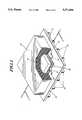
- FIG. 1is a cut-away isometric view of an integrated circuit package in accordance with the invention.
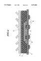
- FIG. 2is a partial cross-sectional view of FIG. 1 through section 2--2 in accordance with the invention.
- FIG. 3is a cross-sectional view of an alternate embodiment of the invention.
- FIG. 4is a cross-sectional view of a further embodiment of the invention.
- FIG. 5is a cross-sectional view of an alternate embodiment of the invention.
- FIG. 6is a block diagram of a radio in accordance with the invention.
- a substrate 10is provided as a circuit carrier.
- the substratemay be made from any one of a number of materials commonly used in the industry, such as epoxy, polyester, polyimide, polyetherimide, polytetrafluoroethylene, glass-reinforced printed circuit board material, metal, ceramic, etc., and may be rigid or flexible. Substrate thicknesses vary from approximately 0.02 mm to 7 mm, with thicknesses ranging from 0.1 mm to 2 mm being preferred.
- the substrate 10has a metallization pattern 13 on an upper or first side 15.
- the metallization pattern 13comprises bonding pads 12 that correspond to bond pads on an integrated circuit (IC) 16.
- One portion of the metallization pattern 13is a grounding pad 17 that comprises a circuit ground.
- solder pads 24on a second side of the substrate 10 is a co-planar array of surface mount solder pads 24.
- the bonding pads 12are electrically connected to the surface mount solder pads 24 by means of conductive through holes 26.
- the solder pads 24comprise an attachment means for surface mounting the semiconductor device package 5 to a larger substrate such as a mother board.
- Surface mounting technology using surface mount padsis well known to those skilled in the art and is also referred to as leadless technology.
- the semiconductor device package 5may also be referred to as a leadless package.
- Solder bumps 23may be optionally attached to the solder pads 24 in order to provide ease of soldering the package to a larger substrate or circuit board.
- pins 18may be attached to the solder pads 24 so as to form a leaded package, or the solder pads could be replaced with pins that fit into holes in the substrate, and are electrically connected to the metallization pattern 13. Such packages would then have an array of pins 18 protruding below the surface of the substrate 10, forming a pin grid array (PGA) package.
- PGApin grid array
- An IC 16such as a semiconductor die or chip, is flip-chip bonded to the bonding pads 12 and the substrate 10.
- This mechanical and electrical attachment to the metallization pattern 13is typically performed by means of metal bumps 22.
- the metal bumps 22are typically solder bumps and the IC 16 is attached using controlled-collapse-chip-connection (C4) technology.
- the metal bumpsmay comprise solder or may also be other materials such as gold, indium, tin, lead, or alloys of these materials.
- the underfill material 25is typically an adhesive, such as an epoxy or an acrylic and has a thermal coefficient of expansion that approximates that of the die and/or the substrate. Examples of underfill materials have been shown in the literature.
- the assemblyis now encapsulated by placing it into a transfer molding cavity and transfer molding a thermoplastic or thermoset molding compound 20. During this operation, the molding compound 20 flows around the IC 16, encapsulating it. The molding compound 20 also encapsulates the underfill material 25 and covers portions or substantially all of the upper surface 15 of the substrate 10.
- Molding compound 20comprises a thermally and electrically conductive material, such as an epoxy, having at least one filler, for example, a metallic element or alloy, which substantially contributes to the thermal and electrical conductive properties of the molding compound.
- the molding compound 20is typically filled to approximately 70% to 75% with copper, aluminum, nickel, gold, silver, or similar type materials to provide electrical and thermal conductivity.
- Suitable encapsulating materialsare sold by Nitto, Sumitomo (1033-B), Nippon Steel, Shinetsu, Ciba-Geigy, Hitachi (EN 4274, or EN 4072), Dexter-Hysol, Dow Chemical, or Shell Chemical.
- the molding compound 20is situated on the upper surface 15 of the substrate 10 such that it provides electrical and mechanical contact to the ground pad 17 and the back surface of the IC 16, which is frequently grounded. As shown in FIGS. 2 and 3, ground pad 17 is also electrically connected by means of a conductive through hole or via 21 to a surface mount solder pad 24 on the bottom side of the substrate 10.
- the electrically conductive molding compound 20now forms not only a cover for the IC 16, but also provides an EMI/RFI shield around the IC in order to form a shielded package. By shielding the package in this manner, external metal shields, as taught in the prior art, are no longer necessary. This solves the problems of the prior art, such as high temperatures transmitted to the IC during the shield attachment process and the additional thickness or bulk associated with the shield.
- the molding material 20can be also formed to provide increased surface area on the top of the package.
- Features such as fins or protrusions 28may be molded directly into the molding compound 20 during the transfer molding operation. Fins 28 provide increased surface area in the top of the package that serves to further enhance the heat-sinking capability of the package 5.
- FIG. 3shows just one of many configurations that the fins 28 may assume. Other types of configurations that enhance the surface area of the top of the package 5 could provide equivalent thermal performance.
- a conventional heat sink 29such as a cast, stamped, or extruded metal structure may be attached to the top of package 5.
- Heat sink 29is typically attached by means of a thermally-conductive material 27, such as thermal grease or solder. Because the overmold compound 20 has a high amount of metallic filler, the metal heat sink 29 can be soldered or welded directly to the molding compound 20.
- the electronic package as described hereinmay find particular use in portable communications applications.
- the RF shielded thermally conductive integrated circuit package 5 of the present inventionis utilized in a radio 30 comprising any well-known radio, such as portable two-way radios manufactured by Motorola Inc., which may operate in either receive or transmit modes.
- the radio 30includes a receiver section 31 and a transmitter section 32 which comprise means for communicating, that is, transmitting or receiving communication signals for the radio.
- the portable radio 30receives a communication signal via an antenna 33.
- a transmit/receive (T/R) switch 34couples the received communication signal to the receiver 31.
- the receiver 31receives and demodulates the received communications signal and presents its audio component to a speaker 36. It may be appreciated by one of ordinary skill in the art that other functions not herein described may be provided by any suitable means, including a controller means (not shown), which controls the entire operation of the radio 30.
- a monolithic integrated circuit packagecomprising a thermally and electrically conductive epoxy that encapsulates at least one semiconductor device or integrated circuit in order to reduce the transfer of unwanted radio frequency energy into or out of the semiconductor package.
- the thermally-conductive materialprovides enhanced heat sinking capability in order to provide an improved package for flip-chip mounting of power RF die.
- the electrically-conductive molded compoundis electrically coupled to a point on the circuit substrate corresponding to a ground plane and forms an RF shield without subjecting the IC to excessive heat. Fins or other projections may be easily molded into the thermally and electrically conductive molding compound in order to provide improved cooling.
Landscapes
- Physics & Mathematics (AREA)
- Engineering & Computer Science (AREA)
- Condensed Matter Physics & Semiconductors (AREA)
- General Physics & Mathematics (AREA)
- Computer Hardware Design (AREA)
- Microelectronics & Electronic Packaging (AREA)
- Power Engineering (AREA)
- Materials Engineering (AREA)
- Chemical & Material Sciences (AREA)
- Health & Medical Sciences (AREA)
- Electromagnetism (AREA)
- Toxicology (AREA)
- Structures Or Materials For Encapsulating Or Coating Semiconductor Devices Or Solid State Devices (AREA)
- Cooling Or The Like Of Semiconductors Or Solid State Devices (AREA)
- Shielding Devices Or Components To Electric Or Magnetic Fields (AREA)
- Wire Bonding (AREA)
Abstract
Description
Claims (16)
Priority Applications (6)
| Application Number | Priority Date | Filing Date | Title |
|---|---|---|---|
| US08/013,391US5371404A (en) | 1993-02-04 | 1993-02-04 | Thermally conductive integrated circuit package with radio frequency shielding |
| DE69428684TDE69428684T2 (en) | 1993-02-04 | 1994-01-24 | THERMAL-CONDUCTIVE HOUSING FOR INTEGRATED CIRCUITS WITH RADIO FREQUENCY SHIELDING |
| JP6518075AJPH08506695A (en) | 1993-02-04 | 1994-01-24 | Thermally conductive integrated circuit package with radio frequency shielding |
| PCT/US1994/000829WO1994018707A1 (en) | 1993-02-04 | 1994-01-24 | Thermally conductive integrated circuit package with radio frequency shielding |
| EP94909485AEP0682812B1 (en) | 1993-02-04 | 1994-01-24 | Thermally conductive integrated circuit package with radio frequency shielding |
| KR1019950703084AKR960700529A (en) | 1993-02-04 | 1995-07-27 | Thermally conductive integrated ciruit package with radio frequency shielding |
Applications Claiming Priority (1)
| Application Number | Priority Date | Filing Date | Title |
|---|---|---|---|
| US08/013,391US5371404A (en) | 1993-02-04 | 1993-02-04 | Thermally conductive integrated circuit package with radio frequency shielding |
Publications (1)
| Publication Number | Publication Date |
|---|---|
| US5371404Atrue US5371404A (en) | 1994-12-06 |
Family
ID=21759717
Family Applications (1)
| Application Number | Title | Priority Date | Filing Date |
|---|---|---|---|
| US08/013,391Expired - LifetimeUS5371404A (en) | 1993-02-04 | 1993-02-04 | Thermally conductive integrated circuit package with radio frequency shielding |
Country Status (6)
| Country | Link |
|---|---|
| US (1) | US5371404A (en) |
| EP (1) | EP0682812B1 (en) |
| JP (1) | JPH08506695A (en) |
| KR (1) | KR960700529A (en) |
| DE (1) | DE69428684T2 (en) |
| WO (1) | WO1994018707A1 (en) |
Cited By (246)
| Publication number | Priority date | Publication date | Assignee | Title |
|---|---|---|---|---|
| US5411199A (en)* | 1994-03-07 | 1995-05-02 | Motorola, Inc. | Method for attaching a shield |
| US5483106A (en)* | 1993-07-30 | 1996-01-09 | Nippondenso Co., Ltd. | Semiconductor device for sensing strain on a substrate |
| US5486720A (en)* | 1994-05-26 | 1996-01-23 | Analog Devices, Inc. | EMF shielding of an integrated circuit package |
| US5510956A (en)* | 1993-11-24 | 1996-04-23 | Fujitsu Limited | Electronic part unit or assembly having a plurality of electronic parts enclosed within a metal enclosure member mounted on a wiring layer |
| US5541449A (en)* | 1994-03-11 | 1996-07-30 | The Panda Project | Semiconductor chip carrier affording a high-density external interface |
| US5543586A (en)* | 1994-03-11 | 1996-08-06 | The Panda Project | Apparatus having inner layers supporting surface-mount components |
| US5576931A (en)* | 1994-05-03 | 1996-11-19 | The Panda Project | Computer with two fans and two air circulation areas |
| US5575688A (en)* | 1992-12-01 | 1996-11-19 | Crane, Jr.; Stanford W. | High-density electrical interconnect system |
| US5583376A (en)* | 1995-01-03 | 1996-12-10 | Motorola, Inc. | High performance semiconductor device with resin substrate and method for making the same |
| US5589711A (en)* | 1993-12-29 | 1996-12-31 | Nec Corporation | Semiconductor package |
| US5600183A (en)* | 1994-11-15 | 1997-02-04 | Hughes Electronics | Multi-layer film adhesive for electrically isolating and grounding an integrated circuit chip to a printed circuit substrate |
| US5619070A (en)* | 1993-12-28 | 1997-04-08 | Kabushiki Kaisha Toshiba | Semiconductor device which radiates heat and applies substrate potential from rear surface of semiconductor chip |
| US5634821A (en)* | 1992-12-01 | 1997-06-03 | Crane, Jr.; Stanford W. | High-density electrical interconnect system |
| US5641996A (en)* | 1995-01-30 | 1997-06-24 | Matsushita Electric Industrial Co., Ltd. | Semiconductor unit package, semiconductor unit packaging method, and encapsulant for use in semiconductor unit packaging |
| US5650593A (en)* | 1994-05-26 | 1997-07-22 | Amkor Electronics, Inc. | Thermally enhanced chip carrier package |
| US5696466A (en)* | 1995-12-08 | 1997-12-09 | The Whitaker Corporation | Heterolithic microwave integrated impedance matching circuitry and method of manufacture |
| US5708567A (en)* | 1995-11-15 | 1998-01-13 | Anam Industrial Co., Ltd. | Ball grid array semiconductor package with ring-type heat sink |
| US5710459A (en)* | 1995-05-12 | 1998-01-20 | Industrial Technology Research Institute | Integrated circuit package provided with multiple heat-conducting paths for enhancing heat dissipation and wrapping around cap for improving integrity and reliability |
| US5744752A (en)* | 1995-06-05 | 1998-04-28 | International Business Machines Corporation | Hermetic thin film metallized sealband for SCM and MCM-D modules |
| US5766982A (en)* | 1996-03-07 | 1998-06-16 | Micron Technology, Inc. | Method and apparatus for underfill of bumped or raised die |
| US5796170A (en)* | 1996-02-15 | 1998-08-18 | Northern Telecom Limited | Ball grid array (BGA) integrated circuit packages |
| US5812797A (en)* | 1994-03-11 | 1998-09-22 | The Panda Project | Computer having a high density connector system |
| US5821457A (en)* | 1994-03-11 | 1998-10-13 | The Panda Project | Semiconductor die carrier having a dielectric epoxy between adjacent leads |
| US5819403A (en)* | 1994-03-11 | 1998-10-13 | The Panda Project | Method of manufacturing a semiconductor chip carrier |
| WO1998028954A3 (en)* | 1996-12-12 | 1998-10-15 | Lsi Logic Corp | Semiconductor packages interconnectably mounted on underlying substrates and methods of producing same |
| US5824950A (en)* | 1994-03-11 | 1998-10-20 | The Panda Project | Low profile semiconductor die carrier |
| US5827999A (en)* | 1994-05-26 | 1998-10-27 | Amkor Electronics, Inc. | Homogeneous chip carrier package |
| US5838545A (en)* | 1996-10-17 | 1998-11-17 | International Business Machines Corporation | High performance, low cost multi-chip modle package |
| EP0863550A3 (en)* | 1997-03-04 | 1999-01-07 | W.L. GORE & ASSOCIATES, INC. | Metallurgical interconnect composite |
| US5864178A (en)* | 1995-01-12 | 1999-01-26 | Kabushiki Kaisha Toshiba | Semiconductor device with improved encapsulating resin |
| EP0818822A3 (en)* | 1996-07-11 | 1999-01-27 | Nokia Mobile Phones Ltd. | Package structure for multichip modules |
| US5866943A (en)* | 1997-06-23 | 1999-02-02 | Lsi Logic Corporation | System and method for forming a grid array device package employing electomagnetic shielding |
| US5866442A (en)* | 1997-01-28 | 1999-02-02 | Micron Technology, Inc. | Method and apparatus for filling a gap between spaced layers of a semiconductor |
| US5877552A (en)* | 1997-06-23 | 1999-03-02 | Industrial Technology Research Institute | Semiconductor package for improving the capability of spreading heat and electrical function |
| US5891753A (en)* | 1997-01-24 | 1999-04-06 | Micron Technology, Inc. | Method and apparatus for packaging flip chip bare die on printed circuit boards |
| US5895229A (en)* | 1997-05-19 | 1999-04-20 | Motorola, Inc. | Microelectronic package including a polymer encapsulated die, and method for forming same |
| US5909057A (en)* | 1997-09-23 | 1999-06-01 | Lsi Logic Corporation | Integrated heat spreader/stiffener with apertures for semiconductor package |
| US5915169A (en)* | 1995-12-22 | 1999-06-22 | Anam Industrial Co., Ltd. | Semiconductor chip scale package and method of producing such |
| US5926696A (en)* | 1994-01-12 | 1999-07-20 | Lucent Technologies Inc. | Ball grid array plastic package |
| US5969426A (en)* | 1994-12-14 | 1999-10-19 | Mitsubishi Denki Kabushiki Kaisha | Substrateless resin encapsulated semiconductor device |
| US5977626A (en)* | 1998-08-12 | 1999-11-02 | Industrial Technology Research Institute | Thermally and electrically enhanced PBGA package |
| US5981312A (en)* | 1997-06-27 | 1999-11-09 | International Business Machines Corporation | Method for injection molded flip chip encapsulation |
| US5982623A (en)* | 1995-01-23 | 1999-11-09 | Matsushita Electric Industrial Co., Ltd. | Module for packaged IC |
| US5990563A (en)* | 1995-12-29 | 1999-11-23 | Lg Semicon Co., Ltd. | Semiconductor package having a connection member |
| WO1999060627A1 (en)* | 1998-05-19 | 1999-11-25 | Siemens Aktiengesellschaft | Electronic module |
| WO1999062119A1 (en)* | 1998-05-22 | 1999-12-02 | Amkor Technology, Inc. | Rf shielded electronic device |
| US5997798A (en)* | 1997-06-27 | 1999-12-07 | International Business Machines Corporation | Biasing mold for integrated circuit chip assembly encapsulation |
| US5998867A (en)* | 1996-02-23 | 1999-12-07 | Honeywell Inc. | Radiation enhanced chip encapsulant |
| US6002171A (en)* | 1997-09-22 | 1999-12-14 | Lsi Logic Corporation | Integrated heat spreader/stiffener assembly and method of assembly for semiconductor package |
| EP0948047A3 (en)* | 1998-03-20 | 1999-12-22 | Caesar Technology Inc. | Electronic component cooling arrangement |
| WO2000008684A1 (en)* | 1998-08-05 | 2000-02-17 | Fairchild Semiconductor Corporation | High performance flip chip package |
| WO2000013233A1 (en)* | 1998-08-28 | 2000-03-09 | Amkor Technology, Inc. | Electromagnetic interference shield device and method |
| WO2000019531A1 (en)* | 1998-09-29 | 2000-04-06 | Conexant Systems, Inc. | Backside electrical contact structure for a module having an exposed backside |
| EP0872889A3 (en)* | 1997-04-16 | 2000-04-19 | DaimlerChrysler Aerospace Aktiengesellschaft | Housing for electronic components |
| US6066509A (en)* | 1998-03-12 | 2000-05-23 | Micron Technology, Inc. | Method and apparatus for underfill of bumped or raised die |
| US6074895A (en)* | 1997-09-23 | 2000-06-13 | International Business Machines Corporation | Method of forming a flip chip assembly |
| US6078102A (en)* | 1998-03-03 | 2000-06-20 | Silicon Bandwidth, Inc. | Semiconductor die package for mounting in horizontal and upright configurations |
| US6081037A (en)* | 1998-06-22 | 2000-06-27 | Motorola, Inc. | Semiconductor component having a semiconductor chip mounted to a chip mount |
| US6097097A (en)* | 1996-08-20 | 2000-08-01 | Fujitsu Limited | Semiconductor device face-down bonded with pillars |
| US6104093A (en)* | 1997-04-24 | 2000-08-15 | International Business Machines Corporation | Thermally enhanced and mechanically balanced flip chip package and method of forming |
| US6108204A (en)* | 1996-01-08 | 2000-08-22 | Intel Corporation | CPU heat sink |
| US6133639A (en)* | 1994-09-20 | 2000-10-17 | Tessera, Inc. | Compliant interface for semiconductor chip and method therefor |
| US6138348A (en)* | 1989-12-18 | 2000-10-31 | Polymer Flip Chip Corporation | Method of forming electrically conductive polymer interconnects on electrical substrates |
| US6140707A (en)* | 1998-05-07 | 2000-10-31 | 3M Innovative Properties Co. | Laminated integrated circuit package |
| WO2000070678A1 (en)* | 1997-10-29 | 2000-11-23 | Hestia Technologies, Inc. | Chip package with molded underfill |
| US6157086A (en)* | 1997-10-29 | 2000-12-05 | Weber; Patrick O. | Chip package with transfer mold underfill |
| US6157085A (en)* | 1998-04-07 | 2000-12-05 | Citizen Watch Co., Ltd. | Semiconductor device for preventing exfoliation from occurring between a semiconductor chip and a resin substrate |
| US6166434A (en)* | 1997-09-23 | 2000-12-26 | Lsi Logic Corporation | Die clip assembly for semiconductor package |
| US6166433A (en)* | 1998-03-26 | 2000-12-26 | Fujitsu Limited | Resin molded semiconductor device and method of manufacturing semiconductor package |
| US6169328B1 (en) | 1994-09-20 | 2001-01-02 | Tessera, Inc | Semiconductor chip assembly |
| US6177728B1 (en)* | 1998-04-28 | 2001-01-23 | International Business Machines Corporation | Integrated circuit chip device having balanced thermal expansion |
| US6184463B1 (en)* | 1998-04-13 | 2001-02-06 | Harris Corporation | Integrated circuit package for flip chip |
| US6191360B1 (en)* | 1999-04-26 | 2001-02-20 | Advanced Semiconductor Engineering, Inc. | Thermally enhanced BGA package |
| WO2001015225A1 (en)* | 1999-08-25 | 2001-03-01 | Telefonaktiebolaget Lm Ericsson (Publ) | A combined heat sink/electromagnetic shield |
| US6228676B1 (en) | 1996-10-31 | 2001-05-08 | Amkor Technology, Inc. | Near chip size integrated circuit package |
| US6255742B1 (en)* | 1997-10-08 | 2001-07-03 | Nec Corporation | Semiconductor package incorporating heat dispersion plate inside resin molding |
| US6262489B1 (en)* | 1999-11-08 | 2001-07-17 | Delphi Technologies, Inc. | Flip chip with backside electrical contact and assembly and method therefor |
| US6265776B1 (en)* | 1998-04-27 | 2001-07-24 | Fry's Metals, Inc. | Flip chip with integrated flux and underfill |
| US6278613B1 (en) | 2000-09-27 | 2001-08-21 | St Assembly Test Services Pte Ltd | Copper pads for heat spreader attach |
| US6284574B1 (en) | 1999-01-04 | 2001-09-04 | International Business Machines Corporation | Method of producing heat dissipating structure for semiconductor devices |
| US6288344B1 (en) | 1999-08-20 | 2001-09-11 | Cardiac Pacemakers, Inc. | Integrated EMI shield utilizing a hybrid edge |
| EP1139412A1 (en)* | 2000-03-30 | 2001-10-04 | Infineon Technologies AG | Flip-chip semiconductor device with backside contact |
| US6324069B1 (en) | 1997-10-29 | 2001-11-27 | Hestia Technologies, Inc. | Chip package with molded underfill |
| EP1160875A1 (en)* | 2000-05-13 | 2001-12-05 | Tyco Electronics AMP GmbH | Electro-optical element with a metal coated housing |
| US6341848B1 (en) | 1999-12-13 | 2002-01-29 | Hewlett-Packard Company | Fluid-jet printer having printhead with integrated heat-sink |
| FR2813146A1 (en)* | 2000-08-21 | 2002-02-22 | Orient Semiconductor Elect Ltd | Improvement of the heat-dissipative structure of a flip chip module involves covering the module completely with an epoxy resin to provide direct contact between the module and resin |
| US20020050632A1 (en)* | 2000-08-31 | 2002-05-02 | Mark Tuttle | Magnetic shielding for integrated circuits |
| US20020053452A1 (en)* | 1996-09-04 | 2002-05-09 | Quan Son Ky | Semiconductor package and method therefor |
| JP2002134987A (en)* | 2000-07-25 | 2002-05-10 | Trw Inc | Packaged electronic device with selectively plated microwave absorbing cover |
| US20020060368A1 (en)* | 2000-04-06 | 2002-05-23 | Tongbi Jiang | Underfile process |
| FR2817445A1 (en)* | 2000-11-28 | 2002-05-31 | Sagem | Mobile telephone screened power integrated circuit having heat dissipation circuit with electromagnetic screen having integrated circuit thermal contact. |
| US6407334B1 (en) | 2000-11-30 | 2002-06-18 | International Business Machines Corporation | I/C chip assembly |
| US6426468B1 (en) | 1997-02-14 | 2002-07-30 | Kabushiki Kaisha Eastern | Circuit board |
| US6448635B1 (en) | 1999-08-30 | 2002-09-10 | Amkor Technology, Inc. | Surface acoustical wave flip chip |
| US20020149092A1 (en)* | 2001-04-11 | 2002-10-17 | Lee Ki Wook | Carrier frame and semiconductor package including carrier frame |
| US20020159235A1 (en)* | 2000-08-04 | 2002-10-31 | Miller James D. | Highly thermally conductive electronic connector |
| US20020168798A1 (en)* | 1996-10-31 | 2002-11-14 | Glenn Thomas P. | Method of making near chip size integrated circuit package |
| US6487077B1 (en)* | 2001-12-10 | 2002-11-26 | Advanced Thermal Technologies | Heat dissipating device adapted to be applied to a flip chip device |
| US20020190396A1 (en)* | 2000-08-16 | 2002-12-19 | Brand Joseph M. | Method and apparatus for removing encapsulating material from a packaged microelectronic device |
| US20030001247A1 (en)* | 2001-06-18 | 2003-01-02 | International Rectifier Corporation | High voltage semiconductor device housing with increased clearance between housing can and die for improved flux flushing |
| US6515861B1 (en)* | 2001-04-02 | 2003-02-04 | Advanced Micro Devices, Inc. | Method and apparatus for shielding electromagnetic emissions from an integrated circuit |
| US6534707B1 (en) | 2000-10-11 | 2003-03-18 | Visteon Global Technologies, Inc. | Method for absorbing active, external and dynamic magnetic fields using a ferrite encapsulated coating |
| US6534859B1 (en)* | 2002-04-05 | 2003-03-18 | St. Assembly Test Services Ltd. | Semiconductor package having heat sink attached to pre-molded cavities and method for creating the package |
| US20030056938A1 (en)* | 2000-02-01 | 2003-03-27 | Mccullough Kevin A. | Heat sink assembly with overmolded carbon matrix |
| US20030067070A1 (en)* | 2001-10-05 | 2003-04-10 | Samsung Electronics Co., Ltd. | Semiconductor package |
| US6546620B1 (en)* | 2000-06-29 | 2003-04-15 | Amkor Technology, Inc. | Flip chip integrated circuit and passive chip component package fabrication method |
| US6552263B2 (en) | 1997-06-27 | 2003-04-22 | International Business Machines Corporation | Method of injection molded flip chip encapsulation |
| US6583987B2 (en)* | 1999-02-26 | 2003-06-24 | Intel Corporation | Electromagnetic interference and heatsinking |
| US20030132531A1 (en)* | 2001-03-28 | 2003-07-17 | Martin Standing | Surface mounted package with die bottom spaced from support board |
| US20030139510A1 (en)* | 2001-11-13 | 2003-07-24 | Sagal E. Mikhail | Polymer compositions having high thermal conductivity and dielectric strength and molded packaging assemblies produced therefrom |
| US20030161511A1 (en)* | 2000-06-09 | 2003-08-28 | Ovidiu Vermesan | Measuring instrument and method for optical measurement of velocity and direction of particles |
| US20030161512A1 (en)* | 2000-06-09 | 2003-08-28 | Svein Mathiassen | Sensor unit, especially for fingerprint sensors |
| US6614102B1 (en) | 2001-05-04 | 2003-09-02 | Amkor Technology, Inc. | Shielded semiconductor leadframe package |
| US6615484B2 (en)* | 1997-09-05 | 2003-09-09 | Litton Systems, Inc. | Method of manufacturing an electrical connection using solder flux compatible with flip chip underfill material |
| US6639757B2 (en) | 2001-01-10 | 2003-10-28 | Hutchinson Technology Inc. | Heat dissipation structures for integrated lead disk drive head suspensions |
| US20040021216A1 (en)* | 2002-07-08 | 2004-02-05 | Futoshi Hosoya | Semiconductor device |
| US20040037042A1 (en)* | 2002-08-20 | 2004-02-26 | Hockanson David M. | EMI shielding apparatus |
| US20040052027A1 (en)* | 2002-09-18 | 2004-03-18 | Sun Microsystems, Inc. | Heat sink and electromagnetic interference reduction device |
| US6713878B2 (en)* | 2001-05-30 | 2004-03-30 | Stmicroelectronics | Electronic element with a shielding |
| US20040074952A1 (en)* | 2002-10-16 | 2004-04-22 | Stipp John N. | Method of controlling solder deposition utilizing two fluxes and preform |
| US20040099940A1 (en)* | 2002-11-22 | 2004-05-27 | International Rectifier Corporation | Semiconductor device having clips for connecting to external elements |
| US20040104489A1 (en)* | 2001-03-28 | 2004-06-03 | International Rectifier Corporation | Direct fet device for high frequency application |
| US6747350B1 (en) | 2003-06-06 | 2004-06-08 | Silicon Integrated Systems Corp. | Flip chip package structure |
| US6750397B2 (en)* | 2002-02-15 | 2004-06-15 | Advanced Semiconductor Engineering, Inc. | Thermally enhanced semiconductor build-up package |
| US20040120117A1 (en)* | 2002-12-20 | 2004-06-24 | Cheng-Why Tan | Electronic package with improved thermal performance |
| US20040124517A1 (en)* | 2002-12-31 | 2004-07-01 | George Hsieh | Structural reinforcement for electronic substrate |
| US20040174651A1 (en)* | 2001-02-15 | 2004-09-09 | Integral Technologies, Inc. | Low cost thermal management device or heat sink manufactured from conductive loaded resin-based materials |
| US20040227225A1 (en)* | 1995-10-31 | 2004-11-18 | Tessera, Inc. | Microelectronic assemblies having compliant layers |
| US20040246065A1 (en)* | 2002-12-31 | 2004-12-09 | Mcnc | Three dimensional multimode and optical coupling devices |
| US20040251522A1 (en)* | 2003-06-10 | 2004-12-16 | Legaspi Severino A. | Electromagnetic interference package protection |
| WO2004109800A1 (en)* | 2003-06-05 | 2004-12-16 | Sony Computer Entertainment Inc. | Electronic device, information processor, and electromagnetic radiation suppressing member |
| US6836022B2 (en) | 2003-02-13 | 2004-12-28 | Medtronic, Inc. | High voltage flip-chip component package and method for forming the same |
| US20050017830A1 (en)* | 2003-05-23 | 2005-01-27 | Kazunori Okui | Enclosure and substrate structure for a tuner module |
| US20050040518A1 (en)* | 2003-08-18 | 2005-02-24 | Brandenburg Scott D. | Process and electronic assembly for removing heat from a circuit device |
| US20050047094A1 (en)* | 2003-08-28 | 2005-03-03 | Shih-Ping Hsu | Heat sink structure with embedded electronic components for semiconductor package |
| US6870272B2 (en) | 1994-09-20 | 2005-03-22 | Tessera, Inc. | Methods of making microelectronic assemblies including compliant interfaces |
| DE10340438A1 (en)* | 2003-09-02 | 2005-04-14 | Epcos Ag | Transmitter module with improved heat dissipation |
| US20050077601A1 (en)* | 2003-10-06 | 2005-04-14 | Gang Yu | Organic electronic devices with low thermal resistance and processes for forming and using the same |
| US20050078468A1 (en)* | 2003-10-09 | 2005-04-14 | Dipoala William S. | Shielding assembly and method |
| WO2005034236A1 (en)* | 2003-09-29 | 2005-04-14 | Siemens Aktiengesellschaft | Plastically deformable cooling body for electric and/or electronic components |
| US20050093132A1 (en)* | 2003-11-05 | 2005-05-05 | Shahla Khorram | RFIC die-package configuration |
| US20050110140A1 (en)* | 2003-11-20 | 2005-05-26 | Taiwan Semiconductor Manufacturing Co. | Heat spreader ball grid array (HSBGA) design for low-k integrated circuits (IC) |
| US20050139994A1 (en)* | 2003-12-31 | 2005-06-30 | Advanced Semiconductor Engineering Inc. | Semiconductor package |
| US20050186707A1 (en)* | 2000-04-04 | 2005-08-25 | International Rectifier Corp. | Chip scale surface mounted device and process of manufacture |
| US20050189646A1 (en)* | 1996-05-24 | 2005-09-01 | Salman Akram | Packaged die on PCB with heat sink encapsulant and methods |
| US20050212098A1 (en)* | 2002-07-31 | 2005-09-29 | Osram Opto Semiconductors Gmbh | Surface-mountable semiconductor component and method for producing it |
| US20050250246A1 (en)* | 2001-09-27 | 2005-11-10 | Hiroshi Ogasawara | Method and apparatus for shielding integrated circuits |
| US6967412B2 (en) | 2001-08-24 | 2005-11-22 | International Rectifier Corporation | Wafer level underfill and interconnect process |
| US20050269677A1 (en)* | 2004-05-28 | 2005-12-08 | Martin Standing | Preparation of front contact for surface mounting |
| US6975512B1 (en)* | 2002-10-31 | 2005-12-13 | Altera Corporation | Thermally enhanced heat sink BGA package |
| US6982481B1 (en)* | 2003-10-08 | 2006-01-03 | Nortel Networks Limited | System for dissipating heat and shielding electromagnetic radiation produced by an electronic device |
| US20060002099A1 (en)* | 2004-06-30 | 2006-01-05 | Stoneham Edward B | Electromagnetic shield assembly |
| FR2872610A1 (en)* | 2004-07-02 | 2006-01-06 | Commissariat Energie Atomique | DEVICE FOR SECURING COMPONENTS |
| US20060022333A1 (en)* | 2000-03-17 | 2006-02-02 | International Rectifier Corporation | Semiconductor multichip module package with improved thermal performance; reduced size and improved moisture resistance |
| US20060054351A1 (en)* | 2003-03-14 | 2006-03-16 | Telefonaktiebolaget Lm Ericsson (Publ) | Substrate structure, a method and an arrangement for producing such substrate structure |
| US20060055006A1 (en)* | 2004-09-16 | 2006-03-16 | Rosemount Inc. | Field device incorporating circuit card assembly as environmental and EMI/RFI shield |
| US20060063300A1 (en)* | 2004-09-22 | 2006-03-23 | Tsorng-Dih Yuan | Structural design for flip-chip assembly |
| US20060084285A1 (en)* | 2002-02-08 | 2006-04-20 | Thomas Muench | Circuit carrier and production thereof |
| US20060091542A1 (en)* | 2004-11-03 | 2006-05-04 | Broadcom Corporation | Flip chip package including a heat spreader having an edge with a recessed edge portion and method of making the same |
| US7082033B1 (en) | 1998-02-13 | 2006-07-25 | Micron Technology, Inc. | Removing heat from integrated circuit devices mounted on a support structure |
| US20060164811A1 (en)* | 2005-01-26 | 2006-07-27 | Maxwell John A | Integral molded heat sinks on DC-DC converters and power supplies |
| US20060175630A1 (en)* | 2003-07-04 | 2006-08-10 | Markus Meier | Electronic power module comprising a rubber seal and corresponding production method |
| US20060194365A1 (en)* | 2005-02-25 | 2006-08-31 | Tessera, Inc. | Microelectronic assemblies having compliancy |
| US20060203453A1 (en)* | 2005-03-08 | 2006-09-14 | Yi Jen Chen | Shielding structure |
| US20060223481A1 (en)* | 2005-03-11 | 2006-10-05 | Takatsugu Kamata | Integrated circuit layout for a television tuner |
| US20060240598A1 (en)* | 2005-04-20 | 2006-10-26 | International Rectifier Corporation | Chip scale package |
| US20060252179A1 (en)* | 2005-05-06 | 2006-11-09 | Neobulb Technologies, Inc. | Integrated circuit packaging structure and method of making the same |
| US20060262510A1 (en)* | 2005-05-18 | 2006-11-23 | Liang-Ming Yu | Electronic element module and electronic device using the same |
| US20060263944A1 (en)* | 2005-05-23 | 2006-11-23 | Texas Instruments Incorporated | System and method for die attach using a backside heat spreader |
| US7164587B1 (en) | 2004-01-14 | 2007-01-16 | Sun Microsystems, Inc. | Integral heatsink grounding arrangement |
| US20070012947A1 (en)* | 2002-07-15 | 2007-01-18 | International Rectifier Corporation | Direct FET device for high frequency application |
| US20070035929A1 (en)* | 2005-08-12 | 2007-02-15 | Hon Hai Precision Industry Co., Ltd. | Heat sink with emi shielding walls |
| US20070051774A1 (en)* | 2005-09-06 | 2007-03-08 | Stipp John N | Method of controlling solder deposition on heat spreader used for semiconductor package |
| US20070063325A1 (en)* | 2005-09-22 | 2007-03-22 | Chun-Hung Lin | Chip package structure and bumping process |
| US7196415B2 (en)* | 2002-03-22 | 2007-03-27 | Broadcom Corporation | Low voltage drop and high thermal performance ball grid array package |
| US20070097650A1 (en)* | 2004-03-31 | 2007-05-03 | Intel Corporation | Electronic packaging apparatus and method |
| US20070107525A1 (en)* | 2005-11-17 | 2007-05-17 | Schnaare Theodore H | Process transmitter with overpressure vent |
| US20070132083A1 (en)* | 2005-12-14 | 2007-06-14 | Lsi Logic Corporation | Semiconductor package having increased resistance to electrostatic discharge |
| US20070166875A1 (en)* | 2005-12-29 | 2007-07-19 | Intel Corporation | Method of forming a microelectronic package and microelectronic package formed according to the method |
| US20070190858A1 (en)* | 2004-06-30 | 2007-08-16 | Endwave Corporation | Electromagnetic shield assembly |
| US7276400B2 (en) | 1996-12-12 | 2007-10-02 | Tessera, Inc. | Methods of making microelectronic packages with conductive elastomeric posts |
| US20070230115A1 (en)* | 2006-02-16 | 2007-10-04 | Stephan Dobritz | Memory module |
| CN100343984C (en)* | 2004-02-27 | 2007-10-17 | 全懋精密科技股份有限公司 | Heat sink structure for semiconductor packaging that can embed electronic components |
| US20080006934A1 (en)* | 2004-11-03 | 2008-01-10 | Broadcom Corporation | Flip Chip Package Including a Non-Planar Heat Spreader and Method of Making the Same |
| US20080017797A1 (en)* | 2006-07-21 | 2008-01-24 | Zhaohui Cheng | Pattern inspection and measurement apparatus |
| US20080093733A1 (en)* | 2006-10-23 | 2008-04-24 | Via Technologies, Inc. | Chip package and manufacturing method thereof |
| US7368325B2 (en) | 2005-04-21 | 2008-05-06 | International Rectifier Corporation | Semiconductor package |
| US20080218971A1 (en)* | 2007-03-05 | 2008-09-11 | International Business Machines Corporation | Method and structure to improve thermal dissipation from semiconductor devices |
| US20080294005A1 (en)* | 2004-09-21 | 2008-11-27 | Takemitsu Honda | Electronic Apparatus |
| US20080289867A1 (en)* | 1994-12-05 | 2008-11-27 | Freescale Semiconductor, Inc. | Multi-strand substrate for ball-grid array assemblies and method |
| US20090014847A1 (en)* | 2007-07-13 | 2009-01-15 | Industrial Technology Research Institute | Integrated circuit package structure with electromagnetic interference shielding structure |
| US20090034206A1 (en)* | 2006-06-30 | 2009-02-05 | Intel Corporation | Wafer-level assembly of heat spreaders for dual ihs packages |
| US20090039515A1 (en)* | 2007-08-10 | 2009-02-12 | International Business Machines Corporation | Ionizing radiation blocking in ic chip to reduce soft errors |
| US20090053459A1 (en)* | 1998-12-16 | 2009-02-26 | Ibiden Co., Ltd. | Conductive connecting pin and package substrate |
| US20090086445A1 (en)* | 2007-10-01 | 2009-04-02 | Denso Corporation | Electronic circuit device and method of making the same |
| US20090086439A1 (en)* | 2007-09-28 | 2009-04-02 | David Whitton | Integrated electrical shield in a heat sink |
| US7579697B2 (en) | 2002-07-15 | 2009-08-25 | International Rectifier Corporation | Arrangement for high frequency application |
| US20090302437A1 (en)* | 2008-06-10 | 2009-12-10 | Stats Chippac, Ltd. | Semiconductor Device and Method of Connecting a Shielding Layer to Ground Through Conductive Vias |
| US7749886B2 (en) | 2006-12-20 | 2010-07-06 | Tessera, Inc. | Microelectronic assemblies having compliancy and methods therefor |
| US20100207153A1 (en)* | 2009-02-18 | 2010-08-19 | Jung Joo Yong | Semiconductor light emitting device and light emitting device package including the same |
| USRE41559E1 (en) | 2001-10-10 | 2010-08-24 | International Rectifier Corporation | Semiconductor device package with improved cooling |
| US20100289135A1 (en)* | 2009-05-15 | 2010-11-18 | Infineon Technologies Ag | Semiconductor chip package |
| EP2302669A1 (en)* | 2004-11-04 | 2011-03-30 | Taiwan Semiconductor Manufacturing Co., Ltd. | Encapsulation material for integrated circuits containing carbon nanotubes |
| DE102010002140A1 (en)* | 2010-02-19 | 2011-08-25 | Robert Bosch GmbH, 70469 | Circuitry has carrier on which power component is received over coupling layer which is formed by mole dynamic mechanical analysis-solid state extrusion (DMA-SSE) portion, connected with the heat sink |
| US8084300B1 (en) | 2010-11-24 | 2011-12-27 | Unisem (Mauritius) Holdings Limited | RF shielding for a singulated laminate semiconductor device package |
| US20120139120A1 (en)* | 2010-12-06 | 2012-06-07 | Stats Chippac, Ltd. | Semiconductor Device and Method of Forming Openings Through Encapsulant to Reduce Warpage and Stress on Semiconductor Package |
| US20120201011A1 (en)* | 2009-11-19 | 2012-08-09 | Parker-Hannifin Corporation | Conductive plastic overmold on shielded plastic window |
| TWI381499B (en)* | 2004-12-20 | 2013-01-01 | 半導體組件工業公司 | Semiconductor package structure having enhanced thermal dissipation characteristics |
| US8466546B2 (en) | 2005-04-22 | 2013-06-18 | International Rectifier Corporation | Chip-scale package |
| US8558386B2 (en) | 1995-10-31 | 2013-10-15 | Tessera, Inc. | Methods of making compliant semiconductor chip packages |
| CN103354228A (en)* | 2013-07-10 | 2013-10-16 | 三星半导体(中国)研究开发有限公司 | Semiconductor packaging part and manufacturing method thereof |
| US8664756B2 (en) | 2012-07-24 | 2014-03-04 | Medtronic, Inc. | Reconstituted wafer package with high voltage discrete active dice and integrated field plate for high temperature leakage current stability |
| CN103681531A (en)* | 2012-09-04 | 2014-03-26 | 英飞凌科技股份有限公司 | Integrated circuits and method for manufacturing integrated circuit |
| US20140168903A1 (en)* | 2012-12-13 | 2014-06-19 | Nvidia Corporation | Passive cooling system integrated into a printed circuit board for cooling electronic components |
| WO2014074933A3 (en)* | 2012-11-09 | 2014-08-07 | Invensas Corporation | Microelectronic assembly with thermally and electrically conductive underfill |
| US20140333505A1 (en)* | 2001-05-17 | 2014-11-13 | Cypress Semiconductor Corporation | Semiconductor package having integrated antenna pad |
| US20140332937A1 (en)* | 2007-04-30 | 2014-11-13 | Markus Brunnbauer | Workpiece with semiconductor chips, semiconductor device and method for producing a workpiece with semiconductor chips |
| US8900503B2 (en) | 2011-09-28 | 2014-12-02 | International Business Machines Corporation | Method of forming an overmolded dual in-line memory module cooling structure |
| US8937376B2 (en) | 2012-04-16 | 2015-01-20 | Advanced Semiconductor Engineering, Inc. | Semiconductor packages with heat dissipation structures and related methods |
| US9122901B2 (en) | 2009-12-29 | 2015-09-01 | Idex Asa | Surface sensor |
| US9214404B1 (en)* | 2011-11-29 | 2015-12-15 | Hrl Laboratories, Llc | Apparatus for mounting microelectronic chips |
| US20160126200A1 (en)* | 2011-07-15 | 2016-05-05 | Samsung Electro-Mechanics Co., Ltd. | Semiconductor device package with integrated antenna for wireless applications |
| WO2016053966A3 (en)* | 2014-09-30 | 2016-06-30 | Henkel IP & Holding GmbH | Temperature regulation using phase change materials contained in an emi can |
| US9385083B1 (en) | 2015-05-22 | 2016-07-05 | Hrl Laboratories, Llc | Wafer-level die to package and die to die interconnects suspended over integrated heat sinks |
| US9501685B2 (en) | 2013-02-22 | 2016-11-22 | Idex Asa | Integrated finger print sensor |
| US9508652B1 (en) | 2015-11-24 | 2016-11-29 | Hrl Laboratories, Llc | Direct IC-to-package wafer level packaging with integrated thermal heat spreaders |
| US9509251B2 (en) | 2015-03-24 | 2016-11-29 | Freescale Semiconductor, Inc. | RF amplifier module and methods of manufacture thereof |
| US20170062376A1 (en)* | 2015-08-28 | 2017-03-02 | Texas Instruments Incorporated | Flip chip backside die grounding techniques |
| CN106653734A (en)* | 2015-11-02 | 2017-05-10 | 晟碟半导体(上海)有限公司 | Semiconductor device with electromagnetic interference shielding and manufacturing method thereof |
| US20170243854A1 (en)* | 2016-02-22 | 2017-08-24 | Taiyo Yuden Co., Ltd. | Circuit substrate and method of manufacturing same |
| US9787254B2 (en)* | 2015-09-23 | 2017-10-10 | Nxp Usa, Inc. | Encapsulated semiconductor device package with heatsink opening, and methods of manufacture thereof |
| US9871107B2 (en) | 2015-05-22 | 2018-01-16 | Nxp Usa, Inc. | Device with a conductive feature formed over a cavity and method therefor |
| US20180197835A1 (en)* | 2015-07-02 | 2018-07-12 | Lumileds Holding B.V. | A surface mount device and a method of attaching such a device |
| US10026672B1 (en) | 2015-10-21 | 2018-07-17 | Hrl Laboratories, Llc | Recursive metal embedded chip assembly |
| US20180226320A1 (en)* | 2017-02-09 | 2018-08-09 | Advanced Semiconductor Engineering, Inc. | Semiconductor package |
| US10075132B2 (en) | 2015-03-24 | 2018-09-11 | Nxp Usa, Inc. | RF amplifier with conductor-less region underlying filter circuit inductor, and methods of manufacture thereof |
| US10079160B1 (en) | 2013-06-21 | 2018-09-18 | Hrl Laboratories, Llc | Surface mount package for semiconductor devices with embedded heat spreaders |
| US10095906B2 (en) | 2014-02-21 | 2018-10-09 | Idex Asa | Sensor employing overlapping grid lines and conductive probes for extending a sensing surface from the grid lines |
| US10157855B2 (en) | 2015-06-03 | 2018-12-18 | Advanced Semiconductor Engineering, Inc. | Semiconductor device including electric and magnetic field shielding |
| US20190035708A1 (en)* | 2017-07-28 | 2019-01-31 | Mstar Semiconductor, Inc. | Circuit board and packaged chip |
| US10212804B2 (en) | 2017-01-16 | 2019-02-19 | Harris Global Communications, Inc. | Electronic device with laterally extending thermally conductive body and related methods |
| US10540534B2 (en)* | 2015-10-29 | 2020-01-21 | Boe Technology Group Co., Ltd. | Electrode structure, fingerprint recognition module and manufacturing method thereof, display device |
| CN111033704A (en)* | 2017-08-31 | 2020-04-17 | 德克萨斯仪器股份有限公司 | Integrated circuit package with stress-inducing material |
| US10950562B1 (en) | 2018-11-30 | 2021-03-16 | Hrl Laboratories, Llc | Impedance-matched through-wafer transition using integrated heat-spreader technology |
| US11189575B1 (en)* | 2020-05-14 | 2021-11-30 | Qualcomm Incorporated | Specialized surface mount device for symmetric heat distribution in package |
| US11691361B2 (en) | 2017-07-28 | 2023-07-04 | Bayerische Motoren Werke Aktiengesellschaft | Method for producing a component, in particular for a motor vehicle, and component |
Families Citing this family (14)
| Publication number | Priority date | Publication date | Assignee | Title |
|---|---|---|---|---|
| JPH07307416A (en)* | 1994-05-12 | 1995-11-21 | Toshiba Corp | Semiconductor chip mounting method and semiconductor device |
| AU3415095A (en)* | 1994-09-06 | 1996-03-27 | Sheldahl, Inc. | Printed circuit substrate having unpackaged integrated circuit chips directly mounted thereto and method of manufacture |
| JP2001523390A (en)* | 1994-12-22 | 2001-11-20 | ベネディクト・ジー・ペース | Module with high mounting efficiency, to which inverted chips are bonded |
| US5904499A (en)* | 1994-12-22 | 1999-05-18 | Pace; Benedict G | Package for power semiconductor chips |
| US6614110B1 (en) | 1994-12-22 | 2003-09-02 | Benedict G Pace | Module with bumps for connection and support |
| GB2378042A (en)* | 2001-07-24 | 2003-01-29 | Ubinetics Ltd | Fixing mechanical parts to PCBs |
| CN1323435C (en)* | 2002-07-19 | 2007-06-27 | 松下电器产业株式会社 | module parts |
| DE10250541B9 (en)* | 2002-10-29 | 2004-09-16 | Infineon Technologies Ag | Electronic component with underfill materials made of thermoplastics and process for its production |
| DE10324421B4 (en)* | 2003-05-28 | 2010-11-25 | Hahn-Schickard-Gesellschaft für angewandte Forschung e.V. | Semiconductor device with Metallisierungsfläche and method for producing the same |
| DE10349775B4 (en)* | 2003-10-24 | 2006-05-11 | Sitronic Gmbh & Co. Kg | Circuit carrier for light-emitting diodes |
| DE102009045063C5 (en) | 2009-09-28 | 2017-06-01 | Infineon Technologies Ag | Power semiconductor module with molded-on heat sink, power semiconductor module system and method for producing a power semiconductor module |
| US9235015B2 (en) | 2013-02-26 | 2016-01-12 | Avago Technologies General Ip (Singapore) Pte. Ltd. | Heat dissipation device and method for use in an optical communications module |
| DE102015120111A1 (en)* | 2015-11-19 | 2017-05-24 | Danfoss Silicon Power Gmbh | The power semiconductor module |
| DE102018216649A1 (en)* | 2018-09-27 | 2020-04-02 | Robert Bosch Gmbh | Electronic assembly |
Citations (13)
| Publication number | Priority date | Publication date | Assignee | Title |
|---|---|---|---|---|
| US2967984A (en)* | 1958-11-03 | 1961-01-10 | Philips Corp | Semiconductor device |
| US3280019A (en)* | 1963-07-03 | 1966-10-18 | Ibm | Method of selectively coating semiconductor chips |
| US3439255A (en)* | 1965-12-02 | 1969-04-15 | Motorola Inc | Encapsulated semiconductor device including a ceramic substrate |
| US3564109A (en)* | 1967-08-24 | 1971-02-16 | Siemens Ag | Semiconductor device with housing |
| US3777221A (en)* | 1972-12-18 | 1973-12-04 | Ibm | Multi-layer circuit package |
| JPS54128276A (en)* | 1978-03-29 | 1979-10-04 | Hitachi Ltd | Resin-sealed semiconductor device |
| US4177480A (en)* | 1975-10-02 | 1979-12-04 | Licentia Patent-Verwaltungs-G.M.B.H. | Integrated circuit arrangement with means for avoiding undesirable capacitive coupling between leads |
| US4278991A (en)* | 1979-08-13 | 1981-07-14 | Burroughs Corporation | IC Package with heat sink and minimal cross-sectional area |
| US4811081A (en)* | 1987-03-23 | 1989-03-07 | Motorola, Inc. | Semiconductor die bonding with conductive adhesive |
| US4825284A (en)* | 1985-12-11 | 1989-04-25 | Hitachi, Ltd. | Semiconductor resin package structure |
| US5113241A (en)* | 1989-12-14 | 1992-05-12 | Kabushiki Kaisha Toshiba | Semiconductor device mounted upon an insulating adhesive with silicon dioxide and nickel chromium steel filling particles |
| US5175613A (en)* | 1991-01-18 | 1992-12-29 | Digital Equipment Corporation | Package for EMI, ESD, thermal, and mechanical shock protection of circuit chips |
| US5218234A (en)* | 1991-12-23 | 1993-06-08 | Motorola, Inc. | Semiconductor device with controlled spread polymeric underfill |
Family Cites Families (7)
| Publication number | Priority date | Publication date | Assignee | Title |
|---|---|---|---|---|
| JPS61276240A (en)* | 1985-05-30 | 1986-12-06 | Mitsubishi Electric Corp | hybrid integrated circuit |
| JPH0294535A (en)* | 1988-09-30 | 1990-04-05 | Nec Corp | Hybrid integrated circuit |
| JPH03214691A (en)* | 1990-01-18 | 1991-09-19 | Fujitsu Ltd | Integrated circuit mounting structure of flexible printed board |
| US5153379A (en)* | 1990-10-09 | 1992-10-06 | Motorola, Inc. | Shielded low-profile electronic component assembly |
| US5166772A (en)* | 1991-02-22 | 1992-11-24 | Motorola, Inc. | Transfer molded semiconductor device package with integral shield |
| US5153385A (en)* | 1991-03-18 | 1992-10-06 | Motorola, Inc. | Transfer molded semiconductor package with improved adhesion |
| US5311059A (en)* | 1992-01-24 | 1994-05-10 | Motorola, Inc. | Backplane grounding for flip-chip integrated circuit |
- 1993
- 1993-02-04USUS08/013,391patent/US5371404A/ennot_activeExpired - Lifetime
- 1994
- 1994-01-24DEDE69428684Tpatent/DE69428684T2/ennot_activeExpired - Lifetime
- 1994-01-24WOPCT/US1994/000829patent/WO1994018707A1/enactiveIP Right Grant
- 1994-01-24EPEP94909485Apatent/EP0682812B1/ennot_activeExpired - Lifetime
- 1994-01-24JPJP6518075Apatent/JPH08506695A/enactivePending
- 1995
- 1995-07-27KRKR1019950703084Apatent/KR960700529A/ennot_activeCeased
Patent Citations (13)
| Publication number | Priority date | Publication date | Assignee | Title |
|---|---|---|---|---|
| US2967984A (en)* | 1958-11-03 | 1961-01-10 | Philips Corp | Semiconductor device |
| US3280019A (en)* | 1963-07-03 | 1966-10-18 | Ibm | Method of selectively coating semiconductor chips |
| US3439255A (en)* | 1965-12-02 | 1969-04-15 | Motorola Inc | Encapsulated semiconductor device including a ceramic substrate |
| US3564109A (en)* | 1967-08-24 | 1971-02-16 | Siemens Ag | Semiconductor device with housing |
| US3777221A (en)* | 1972-12-18 | 1973-12-04 | Ibm | Multi-layer circuit package |
| US4177480A (en)* | 1975-10-02 | 1979-12-04 | Licentia Patent-Verwaltungs-G.M.B.H. | Integrated circuit arrangement with means for avoiding undesirable capacitive coupling between leads |
| JPS54128276A (en)* | 1978-03-29 | 1979-10-04 | Hitachi Ltd | Resin-sealed semiconductor device |
| US4278991A (en)* | 1979-08-13 | 1981-07-14 | Burroughs Corporation | IC Package with heat sink and minimal cross-sectional area |
| US4825284A (en)* | 1985-12-11 | 1989-04-25 | Hitachi, Ltd. | Semiconductor resin package structure |
| US4811081A (en)* | 1987-03-23 | 1989-03-07 | Motorola, Inc. | Semiconductor die bonding with conductive adhesive |
| US5113241A (en)* | 1989-12-14 | 1992-05-12 | Kabushiki Kaisha Toshiba | Semiconductor device mounted upon an insulating adhesive with silicon dioxide and nickel chromium steel filling particles |
| US5175613A (en)* | 1991-01-18 | 1992-12-29 | Digital Equipment Corporation | Package for EMI, ESD, thermal, and mechanical shock protection of circuit chips |
| US5218234A (en)* | 1991-12-23 | 1993-06-08 | Motorola, Inc. | Semiconductor device with controlled spread polymeric underfill |
Cited By (462)
| Publication number | Priority date | Publication date | Assignee | Title |
|---|---|---|---|---|
| US6138348A (en)* | 1989-12-18 | 2000-10-31 | Polymer Flip Chip Corporation | Method of forming electrically conductive polymer interconnects on electrical substrates |
| US5967850A (en)* | 1992-12-01 | 1999-10-19 | Crane, Jr.; Stanford W. | High-density electrical interconnect system |
| US6203347B1 (en) | 1992-12-01 | 2001-03-20 | Silicon Bandwidth Inc. | High-density electrical interconnect system |
| US5951320A (en)* | 1992-12-01 | 1999-09-14 | Crane, Jr.; Stanford W. | Electrical interconnect system with wire receiving portion |
| US5641309A (en)* | 1992-12-01 | 1997-06-24 | Crane, Jr.; Stanford W. | High-density electrical interconnect system |
| US5575688A (en)* | 1992-12-01 | 1996-11-19 | Crane, Jr.; Stanford W. | High-density electrical interconnect system |
| US6554651B2 (en) | 1992-12-01 | 2003-04-29 | Stanford W. Crane, Jr. | High-density electrical interconnect system |
| US5634821A (en)* | 1992-12-01 | 1997-06-03 | Crane, Jr.; Stanford W. | High-density electrical interconnect system |
| US5483106A (en)* | 1993-07-30 | 1996-01-09 | Nippondenso Co., Ltd. | Semiconductor device for sensing strain on a substrate |
| US5510956A (en)* | 1993-11-24 | 1996-04-23 | Fujitsu Limited | Electronic part unit or assembly having a plurality of electronic parts enclosed within a metal enclosure member mounted on a wiring layer |
| US5619070A (en)* | 1993-12-28 | 1997-04-08 | Kabushiki Kaisha Toshiba | Semiconductor device which radiates heat and applies substrate potential from rear surface of semiconductor chip |
| US5589711A (en)* | 1993-12-29 | 1996-12-31 | Nec Corporation | Semiconductor package |
| US5926696A (en)* | 1994-01-12 | 1999-07-20 | Lucent Technologies Inc. | Ball grid array plastic package |
| US5411199A (en)* | 1994-03-07 | 1995-05-02 | Motorola, Inc. | Method for attaching a shield |
| US5822551A (en)* | 1994-03-11 | 1998-10-13 | The Panda Project | Passive backplane capable of being configured to a variable data path width corresponding to a data size of the pluggable CPU board |
| US7103753B2 (en) | 1994-03-11 | 2006-09-05 | Silicon Bandwith Inc. | Backplane system having high-density electrical connectors |
| US5659953A (en)* | 1994-03-11 | 1997-08-26 | The Panda Project | Method of manufacturing an apparatus having inner layers supporting surface-mount components |
| US20040007774A1 (en)* | 1994-03-11 | 2004-01-15 | Silicon Bandwidth, Inc. | Semiconductor chip carrier affording a high-density external interface |
| US5696027A (en)* | 1994-03-11 | 1997-12-09 | The Panda Project | Method of manufacturing a semiconductor chip carrier affording a high-density external interface |
| US6339191B1 (en) | 1994-03-11 | 2002-01-15 | Silicon Bandwidth Inc. | Prefabricated semiconductor chip carrier |
| US20040010638A1 (en)* | 1994-03-11 | 2004-01-15 | Silicon Bandwidth, Inc. | Modular architecture for high bandwidth computers |
| US20100323536A1 (en)* | 1994-03-11 | 2010-12-23 | Wolpass Capital Inv., L.L.C. | Backplane system having high-density electrical connectors |
| US7803020B2 (en) | 1994-03-11 | 2010-09-28 | Crane Jr Stanford W | Backplane system having high-density electrical connectors |
| US5541449A (en)* | 1994-03-11 | 1996-07-30 | The Panda Project | Semiconductor chip carrier affording a high-density external interface |
| US6097086A (en)* | 1994-03-11 | 2000-08-01 | Silicon Bandwidth, Inc. | Semiconductor chip carrier including an interconnect component interface |
| US5812797A (en)* | 1994-03-11 | 1998-09-22 | The Panda Project | Computer having a high density connector system |
| US7183646B2 (en) | 1994-03-11 | 2007-02-27 | Silicon Bandwidth, Inc. | Semiconductor chip carrier affording a high-density external interface |
| US5821457A (en)* | 1994-03-11 | 1998-10-13 | The Panda Project | Semiconductor die carrier having a dielectric epoxy between adjacent leads |
| US5819403A (en)* | 1994-03-11 | 1998-10-13 | The Panda Project | Method of manufacturing a semiconductor chip carrier |
| US6577003B1 (en) | 1994-03-11 | 2003-06-10 | Silicon Bandwidth, Inc. | Semiconductor chip carrier affording a high-density external interface |
| US5824950A (en)* | 1994-03-11 | 1998-10-20 | The Panda Project | Low profile semiconductor die carrier |
| US5543586A (en)* | 1994-03-11 | 1996-08-06 | The Panda Project | Apparatus having inner layers supporting surface-mount components |
| US6574726B2 (en) | 1994-03-11 | 2003-06-03 | Silicon Bandwidth, Inc. | Modular architecture for high bandwidth computers |
| US6977432B2 (en) | 1994-03-11 | 2005-12-20 | Quantum Leap Packaging, Inc. | Prefabricated semiconductor chip carrier |
| US20040140542A1 (en)* | 1994-03-11 | 2004-07-22 | Silicon Bandwidth, Inc. | Prefabricated semiconductor chip carrier |
| US6828511B2 (en) | 1994-03-11 | 2004-12-07 | Silicon Bandwidth Inc. | Prefabricated semiconductor chip carrier |
| US5892280A (en)* | 1994-03-11 | 1999-04-06 | Crane, Jr.; Stanford W. | Semiconductor chip carrier affording a high-density external interface |
| US6073229A (en)* | 1994-03-11 | 2000-06-06 | The Panda Project | Computer system having a modular architecture |
| US5576931A (en)* | 1994-05-03 | 1996-11-19 | The Panda Project | Computer with two fans and two air circulation areas |
| US5781408A (en)* | 1994-05-03 | 1998-07-14 | The Panda Project | Computer system having a motorized door mechanism |
| US5486720A (en)* | 1994-05-26 | 1996-01-23 | Analog Devices, Inc. | EMF shielding of an integrated circuit package |
| US5827999A (en)* | 1994-05-26 | 1998-10-27 | Amkor Electronics, Inc. | Homogeneous chip carrier package |
| US5650593A (en)* | 1994-05-26 | 1997-07-22 | Amkor Electronics, Inc. | Thermally enhanced chip carrier package |
| US20030027374A1 (en)* | 1994-09-20 | 2003-02-06 | Zlata Kovac | Methods of making microelectronic assemblies including compliant interfaces |
| US6521480B1 (en) | 1994-09-20 | 2003-02-18 | Tessera, Inc. | Method for making a semiconductor chip package |
| US6525429B1 (en) | 1994-09-20 | 2003-02-25 | Tessera, Inc. | Methods of making microelectronic assemblies including compliant interfaces |
| US20050139986A1 (en)* | 1994-09-20 | 2005-06-30 | Tessera, Inc. | Methods of making microelectronic assemblies including compliant interfaces |
| US6870272B2 (en) | 1994-09-20 | 2005-03-22 | Tessera, Inc. | Methods of making microelectronic assemblies including compliant interfaces |
| US7368818B2 (en) | 1994-09-20 | 2008-05-06 | Tessera, Inc. | Methods of making microelectronic assemblies including compliant interfaces |
| US6723584B2 (en) | 1994-09-20 | 2004-04-20 | Tessera, Inc. | Methods of making microelectronic assemblies including compliant interfaces |
| US6133639A (en)* | 1994-09-20 | 2000-10-17 | Tessera, Inc. | Compliant interface for semiconductor chip and method therefor |
| US6169328B1 (en) | 1994-09-20 | 2001-01-02 | Tessera, Inc | Semiconductor chip assembly |
| US5600183A (en)* | 1994-11-15 | 1997-02-04 | Hughes Electronics | Multi-layer film adhesive for electrically isolating and grounding an integrated circuit chip to a printed circuit substrate |
| US20080289867A1 (en)* | 1994-12-05 | 2008-11-27 | Freescale Semiconductor, Inc. | Multi-strand substrate for ball-grid array assemblies and method |
| US5969426A (en)* | 1994-12-14 | 1999-10-19 | Mitsubishi Denki Kabushiki Kaisha | Substrateless resin encapsulated semiconductor device |
| US6071755A (en)* | 1994-12-14 | 2000-06-06 | Mitsubushi Denki Kabushiki Kaisha | Method of manufacturing semiconductor device |
| US5583376A (en)* | 1995-01-03 | 1996-12-10 | Motorola, Inc. | High performance semiconductor device with resin substrate and method for making the same |
| US5959363A (en)* | 1995-01-12 | 1999-09-28 | Kabushiki Kaisha Toshiba | Semiconductor device with improved encapsulating resin |
| US5864178A (en)* | 1995-01-12 | 1999-01-26 | Kabushiki Kaisha Toshiba | Semiconductor device with improved encapsulating resin |
| US5982623A (en)* | 1995-01-23 | 1999-11-09 | Matsushita Electric Industrial Co., Ltd. | Module for packaged IC |
| US5641996A (en)* | 1995-01-30 | 1997-06-24 | Matsushita Electric Industrial Co., Ltd. | Semiconductor unit package, semiconductor unit packaging method, and encapsulant for use in semiconductor unit packaging |
| US5710459A (en)* | 1995-05-12 | 1998-01-20 | Industrial Technology Research Institute | Integrated circuit package provided with multiple heat-conducting paths for enhancing heat dissipation and wrapping around cap for improving integrity and reliability |
| US5744752A (en)* | 1995-06-05 | 1998-04-28 | International Business Machines Corporation | Hermetic thin film metallized sealband for SCM and MCM-D modules |
| US7112879B2 (en) | 1995-10-31 | 2006-09-26 | Tessera, Inc. | Microelectronic assemblies having compliant layers |
| US7408260B2 (en) | 1995-10-31 | 2008-08-05 | Tessera, Inc. | Microelectronic assemblies having compliant layers |
| US8338925B2 (en) | 1995-10-31 | 2012-12-25 | Tessera, Inc. | Microelectronic assemblies having compliant layers |
| US20110095441A1 (en)* | 1995-10-31 | 2011-04-28 | Tessera, Inc. | Microelectronic assemblies having compliant layers |
| US7872344B2 (en) | 1995-10-31 | 2011-01-18 | Tessera, Inc. | Microelectronic assemblies having compliant layers |
| US20040227225A1 (en)* | 1995-10-31 | 2004-11-18 | Tessera, Inc. | Microelectronic assemblies having compliant layers |
| US20060237836A1 (en)* | 1995-10-31 | 2006-10-26 | Tessera, Inc. | Microelectronic assemblies having compliant layers |
| US8558386B2 (en) | 1995-10-31 | 2013-10-15 | Tessera, Inc. | Methods of making compliant semiconductor chip packages |
| US5708567A (en)* | 1995-11-15 | 1998-01-13 | Anam Industrial Co., Ltd. | Ball grid array semiconductor package with ring-type heat sink |
| US5696466A (en)* | 1995-12-08 | 1997-12-09 | The Whitaker Corporation | Heterolithic microwave integrated impedance matching circuitry and method of manufacture |
| US5915169A (en)* | 1995-12-22 | 1999-06-22 | Anam Industrial Co., Ltd. | Semiconductor chip scale package and method of producing such |
| US5990563A (en)* | 1995-12-29 | 1999-11-23 | Lg Semicon Co., Ltd. | Semiconductor package having a connection member |
| US6108204A (en)* | 1996-01-08 | 2000-08-22 | Intel Corporation | CPU heat sink |
| US5796170A (en)* | 1996-02-15 | 1998-08-18 | Northern Telecom Limited | Ball grid array (BGA) integrated circuit packages |
| US5998867A (en)* | 1996-02-23 | 1999-12-07 | Honeywell Inc. | Radiation enhanced chip encapsulant |
| US6455933B1 (en) | 1996-03-07 | 2002-09-24 | Micron Technology, Inc. | Underfill of a bumped or raised die utilizing a barrier adjacent to the side wall of flip chip |
| US6376918B1 (en) | 1996-03-07 | 2002-04-23 | Micron Technology, Inc. | Underfill of a bumped or raised die utilizing a barrier adjacent to the side wall of slip chip |
| US6194243B1 (en) | 1996-03-07 | 2001-02-27 | Micron Technology, Inc. | Method of production an underfill of a bumped or raised die using a barrier adjacent to the sidewall of a semiconductor device |
| US20020185748A1 (en)* | 1996-03-07 | 2002-12-12 | Salman Akram | Underfill of a bumped or raised die utilizing a barrier adjacent to the side wall of flip chip |
| US6214635B1 (en) | 1996-03-07 | 2001-04-10 | Micron Technology, Inc. | Method and apparatus for underfill of bumped or raised die |
| US6815817B2 (en) | 1996-03-07 | 2004-11-09 | Micron Technology, Inc. | Underfill of a bumped or raised die utilizing barrier adjacent to the side wall of a flip-chip |
| US5973404A (en)* | 1996-03-07 | 1999-10-26 | Micron Technology, Inc. | Underfill of bumped or raised die using a barrier adjacent to the sidewall of semiconductor device |
| US5766982A (en)* | 1996-03-07 | 1998-06-16 | Micron Technology, Inc. | Method and apparatus for underfill of bumped or raised die |
| US20070069372A1 (en)* | 1996-05-24 | 2007-03-29 | Salman Akram | Packaged die on PCB with heat sink encapsulant and methods |
| US20050189646A1 (en)* | 1996-05-24 | 2005-09-01 | Salman Akram | Packaged die on PCB with heat sink encapsulant and methods |
| EP0818822A3 (en)* | 1996-07-11 | 1999-01-27 | Nokia Mobile Phones Ltd. | Package structure for multichip modules |
| US6097097A (en)* | 1996-08-20 | 2000-08-01 | Fujitsu Limited | Semiconductor device face-down bonded with pillars |
| US20020053452A1 (en)* | 1996-09-04 | 2002-05-09 | Quan Son Ky | Semiconductor package and method therefor |
| US7927927B2 (en) | 1996-09-04 | 2011-04-19 | Freescale Semiconductor, Inc. | Semiconductor package and method therefor |
| US5838545A (en)* | 1996-10-17 | 1998-11-17 | International Business Machines Corporation | High performance, low cost multi-chip modle package |
| US6228676B1 (en) | 1996-10-31 | 2001-05-08 | Amkor Technology, Inc. | Near chip size integrated circuit package |
| US20020168798A1 (en)* | 1996-10-31 | 2002-11-14 | Glenn Thomas P. | Method of making near chip size integrated circuit package |
| US6150193A (en)* | 1996-10-31 | 2000-11-21 | Amkor Technology, Inc. | RF shielded device |
| US6962829B2 (en) | 1996-10-31 | 2005-11-08 | Amkor Technology, Inc. | Method of making near chip size integrated circuit package |
| WO1998028954A3 (en)* | 1996-12-12 | 1998-10-15 | Lsi Logic Corp | Semiconductor packages interconnectably mounted on underlying substrates and methods of producing same |
| US7276400B2 (en) | 1996-12-12 | 2007-10-02 | Tessera, Inc. | Methods of making microelectronic packages with conductive elastomeric posts |
| US5891753A (en)* | 1997-01-24 | 1999-04-06 | Micron Technology, Inc. | Method and apparatus for packaging flip chip bare die on printed circuit boards |
| US6661103B2 (en) | 1997-01-24 | 2003-12-09 | Micron Technology, Inc. | Apparatus for packaging flip chip bare die on printed circuit boards |
| US6400032B1 (en) | 1997-01-24 | 2002-06-04 | Micron Technology, Inc. | Method and apparatus for packaging flip chip bare die on printed circuit boards |
| US6455349B2 (en) | 1997-01-28 | 2002-09-24 | Micron Technology, Inc. | Method and apparatus for filling a gap between spaced layers of a semiconductor |
| US5866442A (en)* | 1997-01-28 | 1999-02-02 | Micron Technology, Inc. | Method and apparatus for filling a gap between spaced layers of a semiconductor |
| US6706555B2 (en) | 1997-01-28 | 2004-03-16 | Micron Technology, Inc. | Method for filling a gap between spaced layers of a semiconductor |
| US6124643A (en)* | 1997-01-28 | 2000-09-26 | Micron Technology, Inc. | Device assembly facilitating gap filling between spaced layers of semiconductor substrates |
| US6685454B2 (en) | 1997-01-28 | 2004-02-03 | Micron Technology, Inc. | Apparatus for filling a gap between spaced layers of a semiconductor |
| US6232145B1 (en) | 1997-01-28 | 2001-05-15 | Micron Technology, Inc. | Method and apparatus for filling a gap between spaced layers of a semiconductor |
| US6443720B1 (en) | 1997-01-28 | 2002-09-03 | Micron Technology, Inc. | Apparatus for filling a gap between spaced layers of a semiconductor |
| US6325606B1 (en) | 1997-01-28 | 2001-12-04 | Micron Technology, Inc. | Apparatus for filling a gap between spaced layers of a semiconductor |
| US6179598B1 (en) | 1997-01-28 | 2001-01-30 | Micron Technology, Inc. | Apparatus for filling a gap between spaced layers of a semiconductor |
| US6426468B1 (en) | 1997-02-14 | 2002-07-30 | Kabushiki Kaisha Eastern | Circuit board |
| EP0863550A3 (en)* | 1997-03-04 | 1999-01-07 | W.L. GORE & ASSOCIATES, INC. | Metallurgical interconnect composite |
| EP0872889A3 (en)* | 1997-04-16 | 2000-04-19 | DaimlerChrysler Aerospace Aktiengesellschaft | Housing for electronic components |
| US6104093A (en)* | 1997-04-24 | 2000-08-15 | International Business Machines Corporation | Thermally enhanced and mechanically balanced flip chip package and method of forming |
| US5895229A (en)* | 1997-05-19 | 1999-04-20 | Motorola, Inc. | Microelectronic package including a polymer encapsulated die, and method for forming same |
| US6093972A (en)* | 1997-05-19 | 2000-07-25 | Motorola, Inc. | Microelectronic package including a polymer encapsulated die |
| US5866943A (en)* | 1997-06-23 | 1999-02-02 | Lsi Logic Corporation | System and method for forming a grid array device package employing electomagnetic shielding |
| US5877552A (en)* | 1997-06-23 | 1999-03-02 | Industrial Technology Research Institute | Semiconductor package for improving the capability of spreading heat and electrical function |
| US6552263B2 (en) | 1997-06-27 | 2003-04-22 | International Business Machines Corporation | Method of injection molded flip chip encapsulation |
| US5997798A (en)* | 1997-06-27 | 1999-12-07 | International Business Machines Corporation | Biasing mold for integrated circuit chip assembly encapsulation |
| US6570261B2 (en) | 1997-06-27 | 2003-05-27 | International Business Machines Corporation | Method and apparatus for injection molded flip chip encapsulation |
| US5981312A (en)* | 1997-06-27 | 1999-11-09 | International Business Machines Corporation | Method for injection molded flip chip encapsulation |
| US6369449B2 (en) | 1997-06-27 | 2002-04-09 | International Business Machines Corporation | Method and apparatus for injection molded flip chip encapsulation |
| US6615484B2 (en)* | 1997-09-05 | 2003-09-09 | Litton Systems, Inc. | Method of manufacturing an electrical connection using solder flux compatible with flip chip underfill material |
| US6002171A (en)* | 1997-09-22 | 1999-12-14 | Lsi Logic Corporation | Integrated heat spreader/stiffener assembly and method of assembly for semiconductor package |
| US6348738B1 (en) | 1997-09-23 | 2002-02-19 | International Business Machines Corporation | Flip chip assembly |
| US5909057A (en)* | 1997-09-23 | 1999-06-01 | Lsi Logic Corporation | Integrated heat spreader/stiffener with apertures for semiconductor package |
| US6166434A (en)* | 1997-09-23 | 2000-12-26 | Lsi Logic Corporation | Die clip assembly for semiconductor package |
| US6074895A (en)* | 1997-09-23 | 2000-06-13 | International Business Machines Corporation | Method of forming a flip chip assembly |
| US6255742B1 (en)* | 1997-10-08 | 2001-07-03 | Nec Corporation | Semiconductor package incorporating heat dispersion plate inside resin molding |
| US6560122B2 (en) | 1997-10-29 | 2003-05-06 | Hestia Technologies, Inc. | Chip package with molded underfill |
| US6324069B1 (en) | 1997-10-29 | 2001-11-27 | Hestia Technologies, Inc. | Chip package with molded underfill |
| WO2000070678A1 (en)* | 1997-10-29 | 2000-11-23 | Hestia Technologies, Inc. | Chip package with molded underfill |
| US6157086A (en)* | 1997-10-29 | 2000-12-05 | Weber; Patrick O. | Chip package with transfer mold underfill |
| US6495083B2 (en) | 1997-10-29 | 2002-12-17 | Hestia Technologies, Inc. | Method of underfilling an integrated circuit chip |
| US7082033B1 (en) | 1998-02-13 | 2006-07-25 | Micron Technology, Inc. | Removing heat from integrated circuit devices mounted on a support structure |
| US6078102A (en)* | 1998-03-03 | 2000-06-20 | Silicon Bandwidth, Inc. | Semiconductor die package for mounting in horizontal and upright configurations |
| US6066509A (en)* | 1998-03-12 | 2000-05-23 | Micron Technology, Inc. | Method and apparatus for underfill of bumped or raised die |
| EP0948047A3 (en)* | 1998-03-20 | 1999-12-22 | Caesar Technology Inc. | Electronic component cooling arrangement |
| US6166433A (en)* | 1998-03-26 | 2000-12-26 | Fujitsu Limited | Resin molded semiconductor device and method of manufacturing semiconductor package |
| US6157085A (en)* | 1998-04-07 | 2000-12-05 | Citizen Watch Co., Ltd. | Semiconductor device for preventing exfoliation from occurring between a semiconductor chip and a resin substrate |
| US6218214B1 (en) | 1998-04-13 | 2001-04-17 | Harris Corporation | Integrated circuit package for flip chip and method of forming same |
| US6184463B1 (en)* | 1998-04-13 | 2001-02-06 | Harris Corporation | Integrated circuit package for flip chip |
| US6265776B1 (en)* | 1998-04-27 | 2001-07-24 | Fry's Metals, Inc. | Flip chip with integrated flux and underfill |
| US6569711B1 (en)* | 1998-04-28 | 2003-05-27 | International Business Machines Corporation | Methods and apparatus for balancing differences in thermal expansion in electronic packaging |
| US6177728B1 (en)* | 1998-04-28 | 2001-01-23 | International Business Machines Corporation | Integrated circuit chip device having balanced thermal expansion |
| US6140707A (en)* | 1998-05-07 | 2000-10-31 | 3M Innovative Properties Co. | Laminated integrated circuit package |
| WO1999060627A1 (en)* | 1998-05-19 | 1999-11-25 | Siemens Aktiengesellschaft | Electronic module |
| WO1999062119A1 (en)* | 1998-05-22 | 1999-12-02 | Amkor Technology, Inc. | Rf shielded electronic device |
| US6081037A (en)* | 1998-06-22 | 2000-06-27 | Motorola, Inc. | Semiconductor component having a semiconductor chip mounted to a chip mount |
| US7537958B1 (en) | 1998-08-05 | 2009-05-26 | Fairchild Semiconductor Corporation | High performance multi-chip flip chip package |
| US7892884B2 (en) | 1998-08-05 | 2011-02-22 | Fairchild Semiconductor Corporation | High performance multi-chip flip chip package |
| US6992384B2 (en) | 1998-08-05 | 2006-01-31 | Fairchild Semiconductor Corporation | High performance multi-chip flip chip package |
| US6133634A (en)* | 1998-08-05 | 2000-10-17 | Fairchild Semiconductor Corporation | High performance flip chip package |
| US6294403B1 (en) | 1998-08-05 | 2001-09-25 | Rajeev Joshi | High performance flip chip package |
| WO2000008684A1 (en)* | 1998-08-05 | 2000-02-17 | Fairchild Semiconductor Corporation | High performance flip chip package |
| US20090230540A1 (en)* | 1998-08-05 | 2009-09-17 | Rajeev Joshi | High performance multi-chip flip chip package |
| US20040159939A1 (en)* | 1998-08-05 | 2004-08-19 | Fairchild Semiconductor Corporation | High performance multi-chip flip chip package |
| US5977626A (en)* | 1998-08-12 | 1999-11-02 | Industrial Technology Research Institute | Thermally and electrically enhanced PBGA package |
| US6092281A (en)* | 1998-08-28 | 2000-07-25 | Amkor Technology, Inc. | Electromagnetic interference shield driver and method |
| US6601293B1 (en) | 1998-08-28 | 2003-08-05 | Amkor Technology, Inc. | Method of making an electromagnetic interference shield device |
| WO2000013233A1 (en)* | 1998-08-28 | 2000-03-09 | Amkor Technology, Inc. | Electromagnetic interference shield device and method |
| WO2000019531A1 (en)* | 1998-09-29 | 2000-04-06 | Conexant Systems, Inc. | Backside electrical contact structure for a module having an exposed backside |
| US20090154131A1 (en)* | 1998-12-16 | 2009-06-18 | Ibiden Co., Ltd. | Conductive connecting pin and package substrate |
| US8110917B2 (en) | 1998-12-16 | 2012-02-07 | Ibiden Co., Ltd. | Package substrate with a conductive connecting pin |
| US7902659B2 (en) | 1998-12-16 | 2011-03-08 | Ibiden Co., Ltd. | Conductive connecting pin and package substrate |
| US20090053459A1 (en)* | 1998-12-16 | 2009-02-26 | Ibiden Co., Ltd. | Conductive connecting pin and package substrate |
| US8035214B1 (en) | 1998-12-16 | 2011-10-11 | Ibiden Co., Ltd. | Conductive connecting pin for package substance |
| US8536696B2 (en) | 1998-12-16 | 2013-09-17 | Ibiden Co., Ltd. | Conductive pin attached to package substrate |
| US20090314537A1 (en)* | 1998-12-16 | 2009-12-24 | Ibiden Co., Ltd. | Conductive connecting pin and package substrate |
| US7847393B2 (en) | 1998-12-16 | 2010-12-07 | Ibiden Co., Ltd. | Conductive connecting pins for a package substrate |
| US6284574B1 (en) | 1999-01-04 | 2001-09-04 | International Business Machines Corporation | Method of producing heat dissipating structure for semiconductor devices |
| US6583987B2 (en)* | 1999-02-26 | 2003-06-24 | Intel Corporation | Electromagnetic interference and heatsinking |
| US6191360B1 (en)* | 1999-04-26 | 2001-02-20 | Advanced Semiconductor Engineering, Inc. | Thermally enhanced BGA package |
| US6865804B2 (en) | 1999-08-20 | 2005-03-15 | Cardiac Pacemakers, Inc. | Method for integrated EMI shielding |
| US20020050401A1 (en)* | 1999-08-20 | 2002-05-02 | Cardiac Pacemakers, Inc. | Integrated EMI shield utilizing a hybrid edge |
| US6288344B1 (en) | 1999-08-20 | 2001-09-11 | Cardiac Pacemakers, Inc. | Integrated EMI shield utilizing a hybrid edge |
| WO2001015225A1 (en)* | 1999-08-25 | 2001-03-01 | Telefonaktiebolaget Lm Ericsson (Publ) | A combined heat sink/electromagnetic shield |
| US6448635B1 (en) | 1999-08-30 | 2002-09-10 | Amkor Technology, Inc. | Surface acoustical wave flip chip |
| US6262489B1 (en)* | 1999-11-08 | 2001-07-17 | Delphi Technologies, Inc. | Flip chip with backside electrical contact and assembly and method therefor |
| US6341848B1 (en) | 1999-12-13 | 2002-01-29 | Hewlett-Packard Company | Fluid-jet printer having printhead with integrated heat-sink |
| US7311140B2 (en) | 2000-02-01 | 2007-12-25 | Cool Options, Inc. | Heat sink assembly with overmolded carbon matrix |
| US20030056938A1 (en)* | 2000-02-01 | 2003-03-27 | Mccullough Kevin A. | Heat sink assembly with overmolded carbon matrix |
| US6680015B2 (en) | 2000-02-01 | 2004-01-20 | Cool Options, Inc. | Method of manufacturing a heat sink assembly with overmolded carbon matrix |
| US8629566B2 (en)* | 2000-03-17 | 2014-01-14 | International Rectifier Corporation | Semiconductor multichip module package with improved thermal performance; reduced size and improved moisture resistance |
| US20060022333A1 (en)* | 2000-03-17 | 2006-02-02 | International Rectifier Corporation | Semiconductor multichip module package with improved thermal performance; reduced size and improved moisture resistance |
| WO2001075964A1 (en)* | 2000-03-30 | 2001-10-11 | Infineon Technologies Ag | Semiconductor element comprising a chip and arrangement with a chip |
| EP1139412A1 (en)* | 2000-03-30 | 2001-10-04 | Infineon Technologies AG | Flip-chip semiconductor device with backside contact |
| US7122887B2 (en) | 2000-04-04 | 2006-10-17 | International Rectifier Corporation | Chip scale surface mounted device and process of manufacture |
| US7253090B2 (en) | 2000-04-04 | 2007-08-07 | International Rectifier Corporation | Chip scale surface mounted device and process of manufacture |
| US20050186707A1 (en)* | 2000-04-04 | 2005-08-25 | International Rectifier Corp. | Chip scale surface mounted device and process of manufacture |
| US20060220123A1 (en)* | 2000-04-04 | 2006-10-05 | International Rectifier Corporation | Chip scale surface mounted device and process of manufacture |
| US7476979B2 (en) | 2000-04-04 | 2009-01-13 | International Rectifier Corporation | Chip scale surface mounted device and process of manufacture |
| US7547579B1 (en) | 2000-04-06 | 2009-06-16 | Micron Technology, Inc. | Underfill process |
| US20020060368A1 (en)* | 2000-04-06 | 2002-05-23 | Tongbi Jiang | Underfile process |
| EP1160875A1 (en)* | 2000-05-13 | 2001-12-05 | Tyco Electronics AMP GmbH | Electro-optical element with a metal coated housing |
| US7518382B2 (en) | 2000-06-09 | 2009-04-14 | Idex Asa | Miniature sensor chip, especially for finger print sensors |
| US20080030207A1 (en)* | 2000-06-09 | 2008-02-07 | Idex Asa | Miniature sensor chip, especially for finger print sensors |
| US20030161512A1 (en)* | 2000-06-09 | 2003-08-28 | Svein Mathiassen | Sensor unit, especially for fingerprint sensors |
| US20030161511A1 (en)* | 2000-06-09 | 2003-08-28 | Ovidiu Vermesan | Measuring instrument and method for optical measurement of velocity and direction of particles |
| US20080002867A1 (en)* | 2000-06-09 | 2008-01-03 | Idex Asa | Sensor unit, especially for fingerprint sensors |
| US7283651B2 (en) | 2000-06-09 | 2007-10-16 | Idex Asa | Measuring instrument and method for optical measurement of velocity and direction of particles |
| US7848550B2 (en) | 2000-06-09 | 2010-12-07 | Idex Asa | Sensor unit, especially for fingerprint sensors |
| US7251351B2 (en) | 2000-06-09 | 2007-07-31 | Idex Asa | Sensor unit, especially for fingerprint sensors |
| US6546620B1 (en)* | 2000-06-29 | 2003-04-15 | Amkor Technology, Inc. | Flip chip integrated circuit and passive chip component package fabrication method |
| JP2002134987A (en)* | 2000-07-25 | 2002-05-10 | Trw Inc | Packaged electronic device with selectively plated microwave absorbing cover |
| US6410847B1 (en)* | 2000-07-25 | 2002-06-25 | Trw Inc. | Packaged electronic system having selectively plated microwave absorbing cover |
| US6851869B2 (en)* | 2000-08-04 | 2005-02-08 | Cool Options, Inc. | Highly thermally conductive electronic connector |
| US20020159235A1 (en)* | 2000-08-04 | 2002-10-31 | Miller James D. | Highly thermally conductive electronic connector |
| US20050095901A1 (en)* | 2000-08-04 | 2005-05-05 | Cool Options, Inc. | Thermally conductive electronic connector having molded housing |
| US6981805B2 (en) | 2000-08-04 | 2006-01-03 | Cool Options, Inc. | Molded electronic connector formed from a thermally conductive polymer composition and method of making the same |
| US7405487B2 (en)* | 2000-08-16 | 2008-07-29 | Micron Technology, Inc. | Method and apparatus for removing encapsulating material from a packaged microelectronic device |
| US20020190396A1 (en)* | 2000-08-16 | 2002-12-19 | Brand Joseph M. | Method and apparatus for removing encapsulating material from a packaged microelectronic device |
| US7273769B1 (en)* | 2000-08-16 | 2007-09-25 | Micron Technology, Inc. | Method and apparatus for removing encapsulating material from a packaged microelectronic device |
| FR2813146A1 (en)* | 2000-08-21 | 2002-02-22 | Orient Semiconductor Elect Ltd | Improvement of the heat-dissipative structure of a flip chip module involves covering the module completely with an epoxy resin to provide direct contact between the module and resin |
| US6717241B1 (en)* | 2000-08-31 | 2004-04-06 | Micron Technology, Inc. | Magnetic shielding for integrated circuits |
| US6924168B2 (en)* | 2000-08-31 | 2005-08-02 | Micron Technology, Inc. | Method of forming a structure for supporting an integrated circuit chip |
| US6559521B2 (en)* | 2000-08-31 | 2003-05-06 | Micron Technology, Inc. | Chip carrier with magnetic shielding |
| US20020050632A1 (en)* | 2000-08-31 | 2002-05-02 | Mark Tuttle | Magnetic shielding for integrated circuits |
| US6278613B1 (en) | 2000-09-27 | 2001-08-21 | St Assembly Test Services Pte Ltd | Copper pads for heat spreader attach |
| SG111014A1 (en)* | 2000-09-27 | 2005-05-30 | Stats Chippac Ltd | Copper pads for heat spreader attach |
| US6534707B1 (en) | 2000-10-11 | 2003-03-18 | Visteon Global Technologies, Inc. | Method for absorbing active, external and dynamic magnetic fields using a ferrite encapsulated coating |
| FR2817445A1 (en)* | 2000-11-28 | 2002-05-31 | Sagem | Mobile telephone screened power integrated circuit having heat dissipation circuit with electromagnetic screen having integrated circuit thermal contact. |
| US6407334B1 (en) | 2000-11-30 | 2002-06-18 | International Business Machines Corporation | I/C chip assembly |
| US6757967B2 (en) | 2000-11-30 | 2004-07-06 | International Business Machines Corporation | Method of forming a chip assembly |
| US6639757B2 (en) | 2001-01-10 | 2003-10-28 | Hutchinson Technology Inc. | Heat dissipation structures for integrated lead disk drive head suspensions |
| US20040174651A1 (en)* | 2001-02-15 | 2004-09-09 | Integral Technologies, Inc. | Low cost thermal management device or heat sink manufactured from conductive loaded resin-based materials |
| US7027304B2 (en)* | 2001-02-15 | 2006-04-11 | Integral Technologies, Inc. | Low cost thermal management device or heat sink manufactured from conductive loaded resin-based materials |
| US20030132531A1 (en)* | 2001-03-28 | 2003-07-17 | Martin Standing | Surface mounted package with die bottom spaced from support board |
| US7285866B2 (en) | 2001-03-28 | 2007-10-23 | International Rectifier Corporation | Surface mounted package with die bottom spaced from support board |
| US6930397B2 (en) | 2001-03-28 | 2005-08-16 | International Rectifier Corporation | Surface mounted package with die bottom spaced from support board |
| US7119447B2 (en) | 2001-03-28 | 2006-10-10 | International Rectifier Corporation | Direct fet device for high frequency application |
| US20040104489A1 (en)* | 2001-03-28 | 2004-06-03 | International Rectifier Corporation | Direct fet device for high frequency application |
| US6515861B1 (en)* | 2001-04-02 | 2003-02-04 | Advanced Micro Devices, Inc. | Method and apparatus for shielding electromagnetic emissions from an integrated circuit |
| US6770961B2 (en)* | 2001-04-11 | 2004-08-03 | Amkor Technology, Inc. | Carrier frame and semiconductor package including carrier frame |
| US20020149092A1 (en)* | 2001-04-11 | 2002-10-17 | Lee Ki Wook | Carrier frame and semiconductor package including carrier frame |
| US6614102B1 (en) | 2001-05-04 | 2003-09-02 | Amkor Technology, Inc. | Shielded semiconductor leadframe package |
| US20140333505A1 (en)* | 2001-05-17 | 2014-11-13 | Cypress Semiconductor Corporation | Semiconductor package having integrated antenna pad |
| US6713878B2 (en)* | 2001-05-30 | 2004-03-30 | Stmicroelectronics | Electronic element with a shielding |
| US7476964B2 (en) | 2001-06-18 | 2009-01-13 | International Rectifier Corporation | High voltage semiconductor device housing with increased clearance between housing can and die for improved flux flushing |
| US20030001247A1 (en)* | 2001-06-18 | 2003-01-02 | International Rectifier Corporation | High voltage semiconductor device housing with increased clearance between housing can and die for improved flux flushing |
| US6967412B2 (en) | 2001-08-24 | 2005-11-22 | International Rectifier Corporation | Wafer level underfill and interconnect process |
| US7005323B2 (en)* | 2001-09-27 | 2006-02-28 | Rfstream Corporation | Method and apparatus for shielding integrated circuits |
| US20050250246A1 (en)* | 2001-09-27 | 2005-11-10 | Hiroshi Ogasawara | Method and apparatus for shielding integrated circuits |
| US20030067070A1 (en)* | 2001-10-05 | 2003-04-10 | Samsung Electronics Co., Ltd. | Semiconductor package |
| US6952050B2 (en)* | 2001-10-05 | 2005-10-04 | Samsung Electronics Co., Ltd. | Semiconductor package |
| USRE41559E1 (en) | 2001-10-10 | 2010-08-24 | International Rectifier Corporation | Semiconductor device package with improved cooling |
| US7476702B2 (en) | 2001-11-13 | 2009-01-13 | Cool Options, Inc. | Polymer electronic device package having high thermal conductivity and dielectric strength |
| US20050189522A1 (en)* | 2001-11-13 | 2005-09-01 | E. Mikhail Sagal | Method of forming an electronic device having high thermal conductivity and dielectric strength |
| US20030139510A1 (en)* | 2001-11-13 | 2003-07-24 | Sagal E. Mikhail | Polymer compositions having high thermal conductivity and dielectric strength and molded packaging assemblies produced therefrom |
| US20050189523A1 (en)* | 2001-11-13 | 2005-09-01 | Sagal E. M. | Polymer electronic device package having high thermal conductivity and dielectric strength |
| US6487077B1 (en)* | 2001-12-10 | 2002-11-26 | Advanced Thermal Technologies | Heat dissipating device adapted to be applied to a flip chip device |
| US20060084285A1 (en)* | 2002-02-08 | 2006-04-20 | Thomas Muench | Circuit carrier and production thereof |
| US7153143B2 (en)* | 2002-02-08 | 2006-12-26 | Infineon Technologies A.G. | Circuit carrier and production thereof |
| US6750397B2 (en)* | 2002-02-15 | 2004-06-15 | Advanced Semiconductor Engineering, Inc. | Thermally enhanced semiconductor build-up package |
| US7781882B2 (en) | 2002-03-22 | 2010-08-24 | Broadcom Corporation | Low voltage drop and high thermal performance ball grid array package |
| US7196415B2 (en)* | 2002-03-22 | 2007-03-27 | Broadcom Corporation | Low voltage drop and high thermal performance ball grid array package |
| US7566590B2 (en) | 2002-03-22 | 2009-07-28 | Broadcom Corporation | Low voltage drop and high thermal performance ball grid array package |
| US6534859B1 (en)* | 2002-04-05 | 2003-03-18 | St. Assembly Test Services Ltd. | Semiconductor package having heat sink attached to pre-molded cavities and method for creating the package |
| US6882040B2 (en)* | 2002-07-08 | 2005-04-19 | Nec Electronics Corporation | Semiconductor device |
| US20040021216A1 (en)* | 2002-07-08 | 2004-02-05 | Futoshi Hosoya | Semiconductor device |
| US20040201034A1 (en)* | 2002-07-08 | 2004-10-14 | Futoshi Hosoya | Semiconductor device |
| US6879033B2 (en)* | 2002-07-08 | 2005-04-12 | Nec Electronics Corporation | Semiconductor device |
| US6853066B2 (en)* | 2002-07-08 | 2005-02-08 | Nec Electronics Corporation | Semiconductor device |
| US20040201092A1 (en)* | 2002-07-08 | 2004-10-14 | Futoshi Hosoya | Semiconductor device |
| US20070012947A1 (en)* | 2002-07-15 | 2007-01-18 | International Rectifier Corporation | Direct FET device for high frequency application |
| US7397137B2 (en) | 2002-07-15 | 2008-07-08 | International Rectifier Corporation | Direct FET device for high frequency application |
| US7579697B2 (en) | 2002-07-15 | 2009-08-25 | International Rectifier Corporation | Arrangement for high frequency application |
| US7199470B2 (en)* | 2002-07-31 | 2007-04-03 | Osram Opto Semiconductors Gmbh | Surface-mountable semiconductor component and method for producing it |
| US20070184629A1 (en)* | 2002-07-31 | 2007-08-09 | Georg Bogner | Method for producing a surface-mountable semiconductor component |
| US7488622B2 (en) | 2002-07-31 | 2009-02-10 | Osram Opto Semiconductors Gmbh | Method for producing a surface-mountable semiconductor component |
| US20050212098A1 (en)* | 2002-07-31 | 2005-09-29 | Osram Opto Semiconductors Gmbh | Surface-mountable semiconductor component and method for producing it |
| US6944025B2 (en)* | 2002-08-20 | 2005-09-13 | Sun Microsystems, Inc. | EMI shielding apparatus |
| US20040037042A1 (en)* | 2002-08-20 | 2004-02-26 | Hockanson David M. | EMI shielding apparatus |
| US7115817B2 (en) | 2002-09-18 | 2006-10-03 | Sun Microsystems, Inc. | Heat sink and electromagnetic interference reduction device |
| US20040052027A1 (en)* | 2002-09-18 | 2004-03-18 | Sun Microsystems, Inc. | Heat sink and electromagnetic interference reduction device |
| US20040074952A1 (en)* | 2002-10-16 | 2004-04-22 | Stipp John N. | Method of controlling solder deposition utilizing two fluxes and preform |
| US6786391B2 (en) | 2002-10-16 | 2004-09-07 | Kac Holdings, Inc. | Method of controlling solder deposition utilizing two fluxes and preform |
| US6975512B1 (en)* | 2002-10-31 | 2005-12-13 | Altera Corporation | Thermally enhanced heat sink BGA package |
| US20040099940A1 (en)* | 2002-11-22 | 2004-05-27 | International Rectifier Corporation | Semiconductor device having clips for connecting to external elements |
| US6841865B2 (en) | 2002-11-22 | 2005-01-11 | International Rectifier Corporation | Semiconductor device having clips for connecting to external elements |
| US20040120117A1 (en)* | 2002-12-20 | 2004-06-24 | Cheng-Why Tan | Electronic package with improved thermal performance |
| US7161238B2 (en)* | 2002-12-31 | 2007-01-09 | Intel Corporation | Structural reinforcement for electronic substrate |
| US6906598B2 (en) | 2002-12-31 | 2005-06-14 | Mcnc | Three dimensional multimode and optical coupling devices |
| US7042306B2 (en) | 2002-12-31 | 2006-05-09 | Research Triangle Institute | Three dimensional multimode and optical coupling devices |
| US20040124517A1 (en)* | 2002-12-31 | 2004-07-01 | George Hsieh | Structural reinforcement for electronic substrate |
| US20040246065A1 (en)* | 2002-12-31 | 2004-12-09 | Mcnc | Three dimensional multimode and optical coupling devices |
| US6836022B2 (en) | 2003-02-13 | 2004-12-28 | Medtronic, Inc. | High voltage flip-chip component package and method for forming the same |
| US7535094B2 (en)* | 2003-03-14 | 2009-05-19 | Telefonaktiebolaget Lm Ericsson (Publ) | Substrate structure, a method and an arrangement for producing such substrate structure |
| US20060054351A1 (en)* | 2003-03-14 | 2006-03-16 | Telefonaktiebolaget Lm Ericsson (Publ) | Substrate structure, a method and an arrangement for producing such substrate structure |
| US7359693B2 (en) | 2003-05-23 | 2008-04-15 | Rfstream Corporation | Enclosure and substrate structure for a tuner module |
| US20050017830A1 (en)* | 2003-05-23 | 2005-01-27 | Kazunori Okui | Enclosure and substrate structure for a tuner module |
| US7053295B2 (en) | 2003-06-05 | 2006-05-30 | Sony Computer Entertainment, Inc. | Electronic device, information processor, and electromagnetic radiation suppressing member |
| US20040257786A1 (en)* | 2003-06-05 | 2004-12-23 | Osamu Murasawa | Electronic device, information processor, and electromagnetic radiation suppressing member |
| WO2004109800A1 (en)* | 2003-06-05 | 2004-12-16 | Sony Computer Entertainment Inc. | Electronic device, information processor, and electromagnetic radiation suppressing member |
| US6747350B1 (en) | 2003-06-06 | 2004-06-08 | Silicon Integrated Systems Corp. | Flip chip package structure |
| US6867480B2 (en)* | 2003-06-10 | 2005-03-15 | Lsi Logic Corporation | Electromagnetic interference package protection |
| US20040251522A1 (en)* | 2003-06-10 | 2004-12-16 | Legaspi Severino A. | Electromagnetic interference package protection |
| US20060175630A1 (en)* | 2003-07-04 | 2006-08-10 | Markus Meier | Electronic power module comprising a rubber seal and corresponding production method |
| US7132746B2 (en)* | 2003-08-18 | 2006-11-07 | Delphi Technologies, Inc. | Electronic assembly with solder-bonded heat sink |
| US20050040518A1 (en)* | 2003-08-18 | 2005-02-24 | Brandenburg Scott D. | Process and electronic assembly for removing heat from a circuit device |
| US7050304B2 (en)* | 2003-08-28 | 2006-05-23 | Phoenix Precision Technology Corporation | Heat sink structure with embedded electronic components for semiconductor package |
| US20050047094A1 (en)* | 2003-08-28 | 2005-03-03 | Shih-Ping Hsu | Heat sink structure with embedded electronic components for semiconductor package |
| US20070108584A1 (en)* | 2003-09-02 | 2007-05-17 | Holger Fluhr | Transmitter module with improved heat dissipation |
| DE10340438B4 (en)* | 2003-09-02 | 2005-08-04 | Epcos Ag | Transmitter module with improved heat dissipation |
| DE10340438A1 (en)* | 2003-09-02 | 2005-04-14 | Epcos Ag | Transmitter module with improved heat dissipation |
| WO2005034236A1 (en)* | 2003-09-29 | 2005-04-14 | Siemens Aktiengesellschaft | Plastically deformable cooling body for electric and/or electronic components |
| US7358665B2 (en) | 2003-10-06 | 2008-04-15 | E. I. Du Pont De Nemours And Company | Organic electronic device provided with a metallic heat sink structure |
| US20050098878A1 (en)* | 2003-10-06 | 2005-05-12 | Gang Yu | Organic electronic devices with low thermal resistance and processes for forming and using the same |
| US7135357B2 (en) | 2003-10-06 | 2006-11-14 | E. I. Du Pont De Nemours And Company | Process for making an organic electronic device having a roughened surface heat sink |
| US20050077601A1 (en)* | 2003-10-06 | 2005-04-14 | Gang Yu | Organic electronic devices with low thermal resistance and processes for forming and using the same |
| US6982481B1 (en)* | 2003-10-08 | 2006-01-03 | Nortel Networks Limited | System for dissipating heat and shielding electromagnetic radiation produced by an electronic device |
| US7009106B2 (en) | 2003-10-09 | 2006-03-07 | Bosch Security Systems, Inc. | Shielding assembly and method |
| US20050078468A1 (en)* | 2003-10-09 | 2005-04-14 | Dipoala William S. | Shielding assembly and method |
| US6998709B2 (en)* | 2003-11-05 | 2006-02-14 | Broadcom Corp. | RFIC die-package configuration |
| US20050093132A1 (en)* | 2003-11-05 | 2005-05-05 | Shahla Khorram | RFIC die-package configuration |
| CN100350599C (en)* | 2003-11-20 | 2007-11-21 | 台湾积体电路制造股份有限公司 | Ball goal array package with heat sink and method of forming same |
| US7180173B2 (en)* | 2003-11-20 | 2007-02-20 | Taiwan Semiconductor Manufacturing Co. Ltd. | Heat spreader ball grid array (HSBGA) design for low-k integrated circuits (IC) |
| US20050110140A1 (en)* | 2003-11-20 | 2005-05-26 | Taiwan Semiconductor Manufacturing Co. | Heat spreader ball grid array (HSBGA) design for low-k integrated circuits (IC) |
| US20050139994A1 (en)* | 2003-12-31 | 2005-06-30 | Advanced Semiconductor Engineering Inc. | Semiconductor package |
| US7164587B1 (en) | 2004-01-14 | 2007-01-16 | Sun Microsystems, Inc. | Integral heatsink grounding arrangement |
| CN100343984C (en)* | 2004-02-27 | 2007-10-17 | 全懋精密科技股份有限公司 | Heat sink structure for semiconductor packaging that can embed electronic components |
| US20070097650A1 (en)* | 2004-03-31 | 2007-05-03 | Intel Corporation | Electronic packaging apparatus and method |
| US7672132B2 (en)* | 2004-03-31 | 2010-03-02 | Intel Corporation | Electronic packaging apparatus and method |
| US20050269677A1 (en)* | 2004-05-28 | 2005-12-08 | Martin Standing | Preparation of front contact for surface mounting |
| US7813145B2 (en) | 2004-06-30 | 2010-10-12 | Endwave Corporation | Circuit structure with multifunction circuit cover |
| US20060002099A1 (en)* | 2004-06-30 | 2006-01-05 | Stoneham Edward B | Electromagnetic shield assembly |
| US20070190858A1 (en)* | 2004-06-30 | 2007-08-16 | Endwave Corporation | Electromagnetic shield assembly |
| FR2872610A1 (en)* | 2004-07-02 | 2006-01-06 | Commissariat Energie Atomique | DEVICE FOR SECURING COMPONENTS |
| US7190053B2 (en) | 2004-09-16 | 2007-03-13 | Rosemount Inc. | Field device incorporating circuit card assembly as environmental and EMI/RFI shield |
| US20060055006A1 (en)* | 2004-09-16 | 2006-03-16 | Rosemount Inc. | Field device incorporating circuit card assembly as environmental and EMI/RFI shield |
| US20080294005A1 (en)* | 2004-09-21 | 2008-11-27 | Takemitsu Honda | Electronic Apparatus |
| US8715163B2 (en) | 2004-09-21 | 2014-05-06 | Olympus Corporation | Electronic apparatus with noise shielding |
| US20060063300A1 (en)* | 2004-09-22 | 2006-03-23 | Tsorng-Dih Yuan | Structural design for flip-chip assembly |
| US7138300B2 (en)* | 2004-09-22 | 2006-11-21 | Taiwan Semiconductor Manufacturing Co., Ltd. | Structural design for flip-chip assembly |
| US7719110B2 (en) | 2004-11-03 | 2010-05-18 | Broadcom Corporation | Flip chip package including a non-planar heat spreader and method of making the same |
| US20060091542A1 (en)* | 2004-11-03 | 2006-05-04 | Broadcom Corporation | Flip chip package including a heat spreader having an edge with a recessed edge portion and method of making the same |
| US20080006934A1 (en)* | 2004-11-03 | 2008-01-10 | Broadcom Corporation | Flip Chip Package Including a Non-Planar Heat Spreader and Method of Making the Same |
| US20110156255A1 (en)* | 2004-11-04 | 2011-06-30 | Koninklijke Philips Electronics N.V. | Carbon nanotube-based filler for integrated circuits |
| EP2302669A1 (en)* | 2004-11-04 | 2011-03-30 | Taiwan Semiconductor Manufacturing Co., Ltd. | Encapsulation material for integrated circuits containing carbon nanotubes |
| TWI381499B (en)* | 2004-12-20 | 2013-01-01 | 半導體組件工業公司 | Semiconductor package structure having enhanced thermal dissipation characteristics |
| US7236368B2 (en)* | 2005-01-26 | 2007-06-26 | Power-One, Inc. | Integral molded heat sinks on DC-DC converters and power supplies |
| US20060164811A1 (en)* | 2005-01-26 | 2006-07-27 | Maxwell John A | Integral molded heat sinks on DC-DC converters and power supplies |
| US7999379B2 (en) | 2005-02-25 | 2011-08-16 | Tessera, Inc. | Microelectronic assemblies having compliancy |
| US20060194365A1 (en)* | 2005-02-25 | 2006-08-31 | Tessera, Inc. | Microelectronic assemblies having compliancy |
| US20060203453A1 (en)* | 2005-03-08 | 2006-09-14 | Yi Jen Chen | Shielding structure |
| US20060223481A1 (en)* | 2005-03-11 | 2006-10-05 | Takatsugu Kamata | Integrated circuit layout for a television tuner |
| US20060240598A1 (en)* | 2005-04-20 | 2006-10-26 | International Rectifier Corporation | Chip scale package |
| US7524701B2 (en) | 2005-04-20 | 2009-04-28 | International Rectifier Corporation | Chip-scale package |
| US20090174058A1 (en)* | 2005-04-20 | 2009-07-09 | International Rectifier Corporation | Chip scale package |
| US8097938B2 (en) | 2005-04-20 | 2012-01-17 | International Rectifier Corporation | Conductive chip-scale package |
| US8061023B2 (en) | 2005-04-21 | 2011-11-22 | International Rectifier Corporation | Process of fabricating a semiconductor package |
| US7368325B2 (en) | 2005-04-21 | 2008-05-06 | International Rectifier Corporation | Semiconductor package |
| US8466546B2 (en) | 2005-04-22 | 2013-06-18 | International Rectifier Corporation | Chip-scale package |
| US7948767B2 (en) | 2005-05-06 | 2011-05-24 | Neobulb Technologies, LLP. | Integrated circuit packaging structure and method of making the same |
| US20100140791A1 (en)* | 2005-05-06 | 2010-06-10 | Neobulb Technologies, Inc. | Integrated circuit packaging structure and method of making the same |
| US20060252179A1 (en)* | 2005-05-06 | 2006-11-09 | Neobulb Technologies, Inc. | Integrated circuit packaging structure and method of making the same |
| US20060262510A1 (en)* | 2005-05-18 | 2006-11-23 | Liang-Ming Yu | Electronic element module and electronic device using the same |
| US7561437B2 (en)* | 2005-05-18 | 2009-07-14 | Chunghwa Picture Tubes, Ltd. | Electronic element module and electronic device using the same |
| US7221055B2 (en)* | 2005-05-23 | 2007-05-22 | Texas Instruments Incorporated | System and method for die attach using a backside heat spreader |
| US20060263944A1 (en)* | 2005-05-23 | 2006-11-23 | Texas Instruments Incorporated | System and method for die attach using a backside heat spreader |
| US20070035929A1 (en)* | 2005-08-12 | 2007-02-15 | Hon Hai Precision Industry Co., Ltd. | Heat sink with emi shielding walls |
| US20070051774A1 (en)* | 2005-09-06 | 2007-03-08 | Stipp John N | Method of controlling solder deposition on heat spreader used for semiconductor package |
| US20070063325A1 (en)* | 2005-09-22 | 2007-03-22 | Chun-Hung Lin | Chip package structure and bumping process |
| US20070107525A1 (en)* | 2005-11-17 | 2007-05-17 | Schnaare Theodore H | Process transmitter with overpressure vent |
| US7287432B2 (en) | 2005-11-17 | 2007-10-30 | Rosemount Inc. | Process transmitter with overpressure vent |
| US20070132083A1 (en)* | 2005-12-14 | 2007-06-14 | Lsi Logic Corporation | Semiconductor package having increased resistance to electrostatic discharge |
| US8258016B2 (en) | 2005-12-14 | 2012-09-04 | Lsi Corporation | Semiconductor package having increased resistance to electrostatic discharge |
| US7498664B2 (en)* | 2005-12-14 | 2009-03-03 | Lsi Corporation | Semiconductor package having increased resistance to electrostatic discharge |
| US20090104735A1 (en)* | 2005-12-14 | 2009-04-23 | Lsi Logic Corporation | Semiconductor package having increased resistance to electrostatic discharge |
| US20070166875A1 (en)* | 2005-12-29 | 2007-07-19 | Intel Corporation | Method of forming a microelectronic package and microelectronic package formed according to the method |
| US20070230115A1 (en)* | 2006-02-16 | 2007-10-04 | Stephan Dobritz | Memory module |
| US20090034206A1 (en)* | 2006-06-30 | 2009-02-05 | Intel Corporation | Wafer-level assembly of heat spreaders for dual ihs packages |
| US20080017797A1 (en)* | 2006-07-21 | 2008-01-24 | Zhaohui Cheng | Pattern inspection and measurement apparatus |
| US20080093733A1 (en)* | 2006-10-23 | 2008-04-24 | Via Technologies, Inc. | Chip package and manufacturing method thereof |
| US8115308B2 (en) | 2006-12-20 | 2012-02-14 | Tessera, Inc. | Microelectronic assemblies having compliancy and methods therefor |
| US20100230812A1 (en)* | 2006-12-20 | 2010-09-16 | Tessera, Inc. | Microelectronic Assemblies Having Compliancy and Methods Therefor |
| US7749886B2 (en) | 2006-12-20 | 2010-07-06 | Tessera, Inc. | Microelectronic assemblies having compliancy and methods therefor |
| US8759973B2 (en) | 2006-12-20 | 2014-06-24 | Tessera, Inc. | Microelectronic assemblies having compliancy and methods therefor |
| US20080310117A1 (en)* | 2007-03-05 | 2008-12-18 | International Business Machines Corporation | Method and structure to improve thermal dissipation from semiconductor devices |
| US7468886B2 (en)* | 2007-03-05 | 2008-12-23 | International Business Machines Corporation | Method and structure to improve thermal dissipation from semiconductor devices |
| US7724527B2 (en) | 2007-03-05 | 2010-05-25 | International Business Machines Corporation | Method and structure to improve thermal dissipation from semiconductor devices |
| US20080218971A1 (en)* | 2007-03-05 | 2008-09-11 | International Business Machines Corporation | Method and structure to improve thermal dissipation from semiconductor devices |
| US20140332937A1 (en)* | 2007-04-30 | 2014-11-13 | Markus Brunnbauer | Workpiece with semiconductor chips, semiconductor device and method for producing a workpiece with semiconductor chips |
| US9601475B2 (en) | 2007-04-30 | 2017-03-21 | Intel Deutschland Gmbh | Workpiece with semiconductor chips, semiconductor device and method for producing a workpiece with semiconductor chips |
| US9293423B2 (en)* | 2007-04-30 | 2016-03-22 | Intel Deutschland Gmbh | Workpiece with semiconductor chips, semiconductor device and method for producing a workpiece with semiconductor chips |
| US20090014847A1 (en)* | 2007-07-13 | 2009-01-15 | Industrial Technology Research Institute | Integrated circuit package structure with electromagnetic interference shielding structure |
| US8999764B2 (en)* | 2007-08-10 | 2015-04-07 | International Business Machines Corporation | Ionizing radiation blocking in IC chip to reduce soft errors |
| US10784200B2 (en) | 2007-08-10 | 2020-09-22 | International Business Machines Corporation | Ionizing radiation blocking in IC chip to reduce soft errors |
| US20090039515A1 (en)* | 2007-08-10 | 2009-02-12 | International Business Machines Corporation | Ionizing radiation blocking in ic chip to reduce soft errors |
| US20090086439A1 (en)* | 2007-09-28 | 2009-04-02 | David Whitton | Integrated electrical shield in a heat sink |
| US7529095B2 (en)* | 2007-09-28 | 2009-05-05 | Visteon Global Technologies, Inc. | Integrated electrical shield in a heat sink |
| US8300419B2 (en)* | 2007-10-01 | 2012-10-30 | Denso Corporation | Electronic circuit device and method of making the same |
| US20090086445A1 (en)* | 2007-10-01 | 2009-04-02 | Denso Corporation | Electronic circuit device and method of making the same |
| US20090302437A1 (en)* | 2008-06-10 | 2009-12-10 | Stats Chippac, Ltd. | Semiconductor Device and Method of Connecting a Shielding Layer to Ground Through Conductive Vias |
| US7851893B2 (en)* | 2008-06-10 | 2010-12-14 | Stats Chippac, Ltd. | Semiconductor device and method of connecting a shielding layer to ground through conductive vias |
| US20100207153A1 (en)* | 2009-02-18 | 2010-08-19 | Jung Joo Yong | Semiconductor light emitting device and light emitting device package including the same |
| US8421103B2 (en)* | 2009-02-18 | 2013-04-16 | Lg Innotek Co., Ltd. | Semiconductor light emitting device and light emitting device package including the same |
| US20100289135A1 (en)* | 2009-05-15 | 2010-11-18 | Infineon Technologies Ag | Semiconductor chip package |
| DE102010016798B4 (en)* | 2009-05-15 | 2016-12-22 | Infineon Technologies Ag | Semiconductor chip package |
| US8933555B2 (en) | 2009-05-15 | 2015-01-13 | Infineon Technologies Ag | Semiconductor chip package |
| US9072162B2 (en)* | 2009-11-19 | 2015-06-30 | Parker-Hannifin Corporation | Conductive plastic overmold on shielded plastic window |
| US20120201011A1 (en)* | 2009-11-19 | 2012-08-09 | Parker-Hannifin Corporation | Conductive plastic overmold on shielded plastic window |
| US9122901B2 (en) | 2009-12-29 | 2015-09-01 | Idex Asa | Surface sensor |
| US9396379B2 (en) | 2009-12-29 | 2016-07-19 | Idex Asa | Surface sensor |
| US10762322B2 (en) | 2009-12-29 | 2020-09-01 | Idex Biometrics Asa | Fingerprint sensor including a substrate defining a ledge with contact points for incorporation into a smartcard |
| DE102010002140A1 (en)* | 2010-02-19 | 2011-08-25 | Robert Bosch GmbH, 70469 | Circuitry has carrier on which power component is received over coupling layer which is formed by mole dynamic mechanical analysis-solid state extrusion (DMA-SSE) portion, connected with the heat sink |
| US8084300B1 (en) | 2010-11-24 | 2011-12-27 | Unisem (Mauritius) Holdings Limited | RF shielding for a singulated laminate semiconductor device package |
| US9171769B2 (en)* | 2010-12-06 | 2015-10-27 | Stats Chippac, Ltd. | Semiconductor device and method of forming openings through encapsulant to reduce warpage and stress on semiconductor package |
| US20120139120A1 (en)* | 2010-12-06 | 2012-06-07 | Stats Chippac, Ltd. | Semiconductor Device and Method of Forming Openings Through Encapsulant to Reduce Warpage and Stress on Semiconductor Package |
| US20160126200A1 (en)* | 2011-07-15 | 2016-05-05 | Samsung Electro-Mechanics Co., Ltd. | Semiconductor device package with integrated antenna for wireless applications |
| US9943936B2 (en) | 2011-09-28 | 2018-04-17 | Lenovo Enterprise Solutions (Singapore) Pte. Ltd. | Overmolded dual in-line memory module cooling structure |
| US8900503B2 (en) | 2011-09-28 | 2014-12-02 | International Business Machines Corporation | Method of forming an overmolded dual in-line memory module cooling structure |
| US9780014B1 (en) | 2011-11-29 | 2017-10-03 | Hrl Laboratories, Llc | Simultaneous controlled depth hot embossing and active side protection during packaging and assembly of wide bandgap devices |
| US9214404B1 (en)* | 2011-11-29 | 2015-12-15 | Hrl Laboratories, Llc | Apparatus for mounting microelectronic chips |
| US8937376B2 (en) | 2012-04-16 | 2015-01-20 | Advanced Semiconductor Engineering, Inc. | Semiconductor packages with heat dissipation structures and related methods |
| US8664756B2 (en) | 2012-07-24 | 2014-03-04 | Medtronic, Inc. | Reconstituted wafer package with high voltage discrete active dice and integrated field plate for high temperature leakage current stability |
| US8749075B2 (en)* | 2012-09-04 | 2014-06-10 | Infineon Technologies Ag | Integrated circuits and a method for manufacturing an integrated circuit |
| CN103681531A (en)* | 2012-09-04 | 2014-03-26 | 英飞凌科技股份有限公司 | Integrated circuits and method for manufacturing integrated circuit |
| DE102013109558B4 (en)* | 2012-09-04 | 2021-05-12 | Infineon Technologies Ag | INTEGRATED CIRCUITS AND METHOD FOR CREATING AN INTEGRATED CIRCUIT |
| CN103681531B (en)* | 2012-09-04 | 2017-03-01 | 英飞凌科技股份有限公司 | Integrated circuit and the method for making integrated circuit |
| WO2014074933A3 (en)* | 2012-11-09 | 2014-08-07 | Invensas Corporation | Microelectronic assembly with thermally and electrically conductive underfill |
| US8847412B2 (en) | 2012-11-09 | 2014-09-30 | Invensas Corporation | Microelectronic assembly with thermally and electrically conductive underfill |
| US20140168903A1 (en)* | 2012-12-13 | 2014-06-19 | Nvidia Corporation | Passive cooling system integrated into a printed circuit board for cooling electronic components |
| US9538633B2 (en)* | 2012-12-13 | 2017-01-03 | Nvidia Corporation | Passive cooling system integrated into a printed circuit board for cooling electronic components |
| US9501685B2 (en) | 2013-02-22 | 2016-11-22 | Idex Asa | Integrated finger print sensor |
| US9881196B2 (en) | 2013-02-22 | 2018-01-30 | Idex Asa | Integrated finger print sensor |
| US10079160B1 (en) | 2013-06-21 | 2018-09-18 | Hrl Laboratories, Llc | Surface mount package for semiconductor devices with embedded heat spreaders |
| CN103354228A (en)* | 2013-07-10 | 2013-10-16 | 三星半导体(中国)研究开发有限公司 | Semiconductor packaging part and manufacturing method thereof |
| US10095906B2 (en) | 2014-02-21 | 2018-10-09 | Idex Asa | Sensor employing overlapping grid lines and conductive probes for extending a sensing surface from the grid lines |
| WO2016053966A3 (en)* | 2014-09-30 | 2016-06-30 | Henkel IP & Holding GmbH | Temperature regulation using phase change materials contained in an emi can |
| US10075132B2 (en) | 2015-03-24 | 2018-09-11 | Nxp Usa, Inc. | RF amplifier with conductor-less region underlying filter circuit inductor, and methods of manufacture thereof |
| US9509251B2 (en) | 2015-03-24 | 2016-11-29 | Freescale Semiconductor, Inc. | RF amplifier module and methods of manufacture thereof |
| US9871107B2 (en) | 2015-05-22 | 2018-01-16 | Nxp Usa, Inc. | Device with a conductive feature formed over a cavity and method therefor |
| US9837372B1 (en) | 2015-05-22 | 2017-12-05 | Hrl Laboratories, Llc | Wafer-level die to package and die to die interconnects suspended over integrated heat sinks |
| US9385083B1 (en) | 2015-05-22 | 2016-07-05 | Hrl Laboratories, Llc | Wafer-level die to package and die to die interconnects suspended over integrated heat sinks |
| US10157855B2 (en) | 2015-06-03 | 2018-12-18 | Advanced Semiconductor Engineering, Inc. | Semiconductor device including electric and magnetic field shielding |
| US20180197835A1 (en)* | 2015-07-02 | 2018-07-12 | Lumileds Holding B.V. | A surface mount device and a method of attaching such a device |
| US11043467B2 (en) | 2015-08-28 | 2021-06-22 | Texas Instruments Incorporated | Flip chip backside die grounding techniques |
| US10607958B2 (en)* | 2015-08-28 | 2020-03-31 | Texas Instruments Incorporated | Flip chip backside die grounding techniques |
| US20170062376A1 (en)* | 2015-08-28 | 2017-03-02 | Texas Instruments Incorporated | Flip chip backside die grounding techniques |
| US9787254B2 (en)* | 2015-09-23 | 2017-10-10 | Nxp Usa, Inc. | Encapsulated semiconductor device package with heatsink opening, and methods of manufacture thereof |
| US10630246B2 (en)* | 2015-09-23 | 2020-04-21 | Nxp Usa, Inc. | Methods of manufacturing encapsulated semiconductor device package with heatsink opening |
| US10026672B1 (en) | 2015-10-21 | 2018-07-17 | Hrl Laboratories, Llc | Recursive metal embedded chip assembly |
| US10483184B1 (en) | 2015-10-21 | 2019-11-19 | Hrl Laboratories, Llc | Recursive metal embedded chip assembly |
| US10540534B2 (en)* | 2015-10-29 | 2020-01-21 | Boe Technology Group Co., Ltd. | Electrode structure, fingerprint recognition module and manufacturing method thereof, display device |
| CN106653734A (en)* | 2015-11-02 | 2017-05-10 | 晟碟半导体(上海)有限公司 | Semiconductor device with electromagnetic interference shielding and manufacturing method thereof |
| US9508652B1 (en) | 2015-11-24 | 2016-11-29 | Hrl Laboratories, Llc | Direct IC-to-package wafer level packaging with integrated thermal heat spreaders |
| US20170243854A1 (en)* | 2016-02-22 | 2017-08-24 | Taiyo Yuden Co., Ltd. | Circuit substrate and method of manufacturing same |
| US10050014B2 (en)* | 2016-02-22 | 2018-08-14 | Taiyo Yuden Co., Ltd. | Circuit substrate and method of manufacturing same |
| US10212804B2 (en) | 2017-01-16 | 2019-02-19 | Harris Global Communications, Inc. | Electronic device with laterally extending thermally conductive body and related methods |
| US20180226320A1 (en)* | 2017-02-09 | 2018-08-09 | Advanced Semiconductor Engineering, Inc. | Semiconductor package |
| US11075186B2 (en)* | 2017-02-09 | 2021-07-27 | Advanced Semiconductor Engineering, Inc. | Semiconductor package |
| US10559513B2 (en)* | 2017-07-28 | 2020-02-11 | Mediatek Inc. | Circuit board and packaged chip |
| US20190035708A1 (en)* | 2017-07-28 | 2019-01-31 | Mstar Semiconductor, Inc. | Circuit board and packaged chip |
| US11296006B2 (en) | 2017-07-28 | 2022-04-05 | Mediatek Inc. | Circuit board and packaged chip |
| US11691361B2 (en) | 2017-07-28 | 2023-07-04 | Bayerische Motoren Werke Aktiengesellschaft | Method for producing a component, in particular for a motor vehicle, and component |
| CN111033704A (en)* | 2017-08-31 | 2020-04-17 | 德克萨斯仪器股份有限公司 | Integrated circuit package with stress-inducing material |
| CN111033704B (en)* | 2017-08-31 | 2023-10-20 | 德克萨斯仪器股份有限公司 | Integrated circuit package with stress directing material |
| US10950562B1 (en) | 2018-11-30 | 2021-03-16 | Hrl Laboratories, Llc | Impedance-matched through-wafer transition using integrated heat-spreader technology |
| US11189575B1 (en)* | 2020-05-14 | 2021-11-30 | Qualcomm Incorporated | Specialized surface mount device for symmetric heat distribution in package |
Also Published As
| Publication number | Publication date |
|---|---|
| KR960700529A (en) | 1996-01-20 |
| JPH08506695A (en) | 1996-07-16 |
| DE69428684T2 (en) | 2002-08-01 |
| WO1994018707A1 (en) | 1994-08-18 |
| EP0682812A4 (en) | 1998-04-15 |
| EP0682812B1 (en) | 2001-10-17 |
| EP0682812A1 (en) | 1995-11-22 |
| DE69428684D1 (en) | 2001-11-22 |
Similar Documents
| Publication | Publication Date | Title |
|---|---|---|
| US5371404A (en) | Thermally conductive integrated circuit package with radio frequency shielding | |
| US5166772A (en) | Transfer molded semiconductor device package with integral shield | |
| US5557142A (en) | Shielded semiconductor device package | |
| US6809931B2 (en) | Heat sink apparatus that provides electrical isolation for integrally shielded circuit | |
| KR100590382B1 (en) | Electronic package and manufacturing method thereof | |
| US5397917A (en) | Semiconductor package capable of spreading heat | |
| US7268426B2 (en) | High-frequency chip packages | |
| US5619070A (en) | Semiconductor device which radiates heat and applies substrate potential from rear surface of semiconductor chip | |
| US6813154B2 (en) | Reversible heat sink packaging assembly for an integrated circuit | |
| US5436203A (en) | Shielded liquid encapsulated semiconductor device and method for making the same | |
| JP3407971B2 (en) | Integrated circuit package and assembly structure thereof | |
| US6580167B1 (en) | Heat spreader with spring IC package | |
| US6562655B1 (en) | Heat spreader with spring IC package fabrication method | |
| US6396699B1 (en) | Heat sink with chip die EMC ground interconnect | |
| US11373960B2 (en) | Electronic component module | |
| JP3148718B2 (en) | Thermally and electrically enhanced semiconductor package | |
| CN216354159U (en) | Packaging structure of radio frequency module and communication device | |
| JP3492594B2 (en) | Semiconductor module | |
| KR100698570B1 (en) | Package device with electromagnetic interference shield | |
| US6437984B1 (en) | Thermally enhanced chip scale package | |
| JP2001035957A (en) | Package for storing electronic components, semiconductor device and package manufacturing method | |
| JP3506547B2 (en) | Semiconductor device | |
| EP0996155A2 (en) | Radio frequency integrated circuit apparatus | |
| GB2307596A (en) | Radio communications module | |
| JP2927184B2 (en) | Microwave circuit mounting structure |
Legal Events
| Date | Code | Title | Description |
|---|---|---|---|
| AS | Assignment | Owner name:MOTOROLA, INC., ILLINOIS Free format text:ASSIGNMENT OF ASSIGNORS INTEREST.;ASSIGNORS:JUSKEY, FRANK J.;SUPPELSA, ANTHONY B.;REEL/FRAME:006427/0594 Effective date:19930129 | |
| STCF | Information on status: patent grant | Free format text:PATENTED CASE | |
| FPAY | Fee payment | Year of fee payment:4 | |
| FPAY | Fee payment | Year of fee payment:8 | |
| REMI | Maintenance fee reminder mailed | ||
| AS | Assignment | Owner name:FREESCALE SEMICONDUCTOR, INC., TEXAS Free format text:ASSIGNMENT OF ASSIGNORS INTEREST;ASSIGNOR:MOTOROLA, INC.;REEL/FRAME:015698/0657 Effective date:20040404 Owner name:FREESCALE SEMICONDUCTOR, INC.,TEXAS Free format text:ASSIGNMENT OF ASSIGNORS INTEREST;ASSIGNOR:MOTOROLA, INC.;REEL/FRAME:015698/0657 Effective date:20040404 | |
| FPAY | Fee payment | Year of fee payment:12 | |
| AS | Assignment | Owner name:CITIBANK, N.A. AS COLLATERAL AGENT, NEW YORK Free format text:SECURITY AGREEMENT;ASSIGNORS:FREESCALE SEMICONDUCTOR, INC.;FREESCALE ACQUISITION CORPORATION;FREESCALE ACQUISITION HOLDINGS CORP.;AND OTHERS;REEL/FRAME:018855/0129 Effective date:20061201 Owner name:CITIBANK, N.A. AS COLLATERAL AGENT,NEW YORK Free format text:SECURITY AGREEMENT;ASSIGNORS:FREESCALE SEMICONDUCTOR, INC.;FREESCALE ACQUISITION CORPORATION;FREESCALE ACQUISITION HOLDINGS CORP.;AND OTHERS;REEL/FRAME:018855/0129 Effective date:20061201 | |
| AS | Assignment | Owner name:CITIBANK, N.A., AS COLLATERAL AGENT,NEW YORK Free format text:SECURITY AGREEMENT;ASSIGNOR:FREESCALE SEMICONDUCTOR, INC.;REEL/FRAME:024397/0001 Effective date:20100413 Owner name:CITIBANK, N.A., AS COLLATERAL AGENT, NEW YORK Free format text:SECURITY AGREEMENT;ASSIGNOR:FREESCALE SEMICONDUCTOR, INC.;REEL/FRAME:024397/0001 Effective date:20100413 | |
| AS | Assignment | Owner name:FREESCALE SEMICONDUCTOR, INC., TEXAS Free format text:PATENT RELEASE;ASSIGNOR:CITIBANK, N.A., AS COLLATERAL AGENT;REEL/FRAME:037354/0225 Effective date:20151207 Owner name:FREESCALE SEMICONDUCTOR, INC., TEXAS Free format text:PATENT RELEASE;ASSIGNOR:CITIBANK, N.A., AS COLLATERAL AGENT;REEL/FRAME:037356/0143 Effective date:20151207 Owner name:FREESCALE SEMICONDUCTOR, INC., TEXAS Free format text:PATENT RELEASE;ASSIGNOR:CITIBANK, N.A., AS COLLATERAL AGENT;REEL/FRAME:037356/0553 Effective date:20151207 |