US5371025A - Method of making thin film transistors - Google Patents
Method of making thin film transistorsDownload PDFInfo
- Publication number
- US5371025A US5371025AUS07/940,060US94006092AUS5371025AUS 5371025 AUS5371025 AUS 5371025AUS 94006092 AUS94006092 AUS 94006092AUS 5371025 AUS5371025 AUS 5371025A
- Authority
- US
- United States
- Prior art keywords
- layer
- refractory metal
- pattern
- gate electrode
- insulating layer
- Prior art date
- Legal status (The legal status is an assumption and is not a legal conclusion. Google has not performed a legal analysis and makes no representation as to the accuracy of the status listed.)
- Expired - Lifetime
Links
Images


Classifications
- H—ELECTRICITY
- H10—SEMICONDUCTOR DEVICES; ELECTRIC SOLID-STATE DEVICES NOT OTHERWISE PROVIDED FOR
- H10D—INORGANIC ELECTRIC SEMICONDUCTOR DEVICES
- H10D30/00—Field-effect transistors [FET]
- H10D30/01—Manufacture or treatment
- H10D30/021—Manufacture or treatment of FETs having insulated gates [IGFET]
- H10D30/031—Manufacture or treatment of FETs having insulated gates [IGFET] of thin-film transistors [TFT]
- H10D30/0321—Manufacture or treatment of FETs having insulated gates [IGFET] of thin-film transistors [TFT] comprising silicon, e.g. amorphous silicon or polysilicon
- H—ELECTRICITY
- H01—ELECTRIC ELEMENTS
- H01L—SEMICONDUCTOR DEVICES NOT COVERED BY CLASS H10
- H01L21/00—Processes or apparatus adapted for the manufacture or treatment of semiconductor or solid state devices or of parts thereof
- H01L21/02—Manufacture or treatment of semiconductor devices or of parts thereof
- H01L21/027—Making masks on semiconductor bodies for further photolithographic processing not provided for in group H01L21/18 or H01L21/34
- H01L21/0271—Making masks on semiconductor bodies for further photolithographic processing not provided for in group H01L21/18 or H01L21/34 comprising organic layers
- H01L21/0273—Making masks on semiconductor bodies for further photolithographic processing not provided for in group H01L21/18 or H01L21/34 comprising organic layers characterised by the treatment of photoresist layers
- H01L21/0274—Photolithographic processes
- H—ELECTRICITY
- H10—SEMICONDUCTOR DEVICES; ELECTRIC SOLID-STATE DEVICES NOT OTHERWISE PROVIDED FOR
- H10D—INORGANIC ELECTRIC SEMICONDUCTOR DEVICES
- H10D30/00—Field-effect transistors [FET]
- H10D30/01—Manufacture or treatment
- H10D30/021—Manufacture or treatment of FETs having insulated gates [IGFET]
- H10D30/031—Manufacture or treatment of FETs having insulated gates [IGFET] of thin-film transistors [TFT]
- H10D30/0312—Manufacture or treatment of FETs having insulated gates [IGFET] of thin-film transistors [TFT] characterised by the gate electrodes
- H10D30/0316—Manufacture or treatment of FETs having insulated gates [IGFET] of thin-film transistors [TFT] characterised by the gate electrodes of lateral bottom-gate TFTs comprising only a single gate
- H—ELECTRICITY
- H10—SEMICONDUCTOR DEVICES; ELECTRIC SOLID-STATE DEVICES NOT OTHERWISE PROVIDED FOR
- H10D—INORGANIC ELECTRIC SEMICONDUCTOR DEVICES
- H10D30/00—Field-effect transistors [FET]
- H10D30/60—Insulated-gate field-effect transistors [IGFET]
- H10D30/67—Thin-film transistors [TFT]
- H10D30/6729—Thin-film transistors [TFT] characterised by the electrodes
- H10D30/6737—Thin-film transistors [TFT] characterised by the electrodes characterised by the electrode materials
- H—ELECTRICITY
- H10—SEMICONDUCTOR DEVICES; ELECTRIC SOLID-STATE DEVICES NOT OTHERWISE PROVIDED FOR
- H10D—INORGANIC ELECTRIC SEMICONDUCTOR DEVICES
- H10D30/00—Field-effect transistors [FET]
- H10D30/60—Insulated-gate field-effect transistors [IGFET]
- H10D30/67—Thin-film transistors [TFT]
- H10D30/674—Thin-film transistors [TFT] characterised by the active materials
- H10D30/6741—Group IV materials, e.g. germanium or silicon carbide
- H10D30/6743—Silicon
- H—ELECTRICITY
- H10—SEMICONDUCTOR DEVICES; ELECTRIC SOLID-STATE DEVICES NOT OTHERWISE PROVIDED FOR
- H10D—INORGANIC ELECTRIC SEMICONDUCTOR DEVICES
- H10D30/00—Field-effect transistors [FET]
- H10D30/60—Insulated-gate field-effect transistors [IGFET]
- H10D30/67—Thin-film transistors [TFT]
- H10D30/6757—Thin-film transistors [TFT] characterised by the structure of the channel, e.g. transverse or longitudinal shape or doping profile
Definitions
- the present inventionrelates to a method of making thin film transistors, and more particularly to a method of making thin film transistors suitable in forming a high quality of thin film transistors-liquid crystal displays in a large area.
- FIG. 1shows an equivalent circuit for one pixel in such a TFT-LCD.
- each pixel electrodeSupplying of voltage to each pixel electrode is carried out via a signal line by a corresponding thin film transistor which is switched by a gate voltage supplied via a gate bus line.
- a parasitic capacitance (Cgd)is inevitably present between a gate and a drain of the transistor.
- the parasitic capacitance Cgdcauses a feed-through of the pixel electrode voltage, as shown in FIG. 1.
- This feed-through voltage Vcan be expressed by the following formula 1: ##EQU1## where, Cic and Cst are other parasitic capacitances.
- the feed-through voltage Vacts to break the balance of the voltage applied to the liquid crystal, resulting in flickering of the LCD and a decrease in the reliability.
- the Cstshould be sufficiently large, as compared with the Cgd.
- the TFT-LCDhas a larger size and a higher pixel density, the Cic increases and the charging time decreases. Accordingly, charging for the enlarged Cic should be in a shortened charging time.
- the value of W/L(where, W is the channel width of TFT and L is the channel length of TFT) should be increased, which determines the value of ON current for TFT, where L is constant, W and Cgd increase.
- the Cstshould be increased more.
- the resistance for a SC linecan not be decreased to a small value. This is because of a limitation on pixel aperture rate. As a result, it is difficult to control the SC electrode voltage at a larger size of the display.
- To decrease the Cgdis the most efficient method for solving this problem.
- the generation of the Cgdresults from an overlap between the gate electrode and the source/drain electrodes. However, this overlap is necessarily present in case of an inverted staggered type TFT and can not be reduced below 2 ⁇ m due to an accuracy in mask alignment required for a large size of the display.
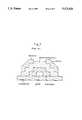
- FIG. 2there is illustrated a general inverted staggered type TFT which is characterized by an insulation layer and a semiconductor layer formed on a gate electrode.
- the overlapcan be extremely reduced by self-aligning the source/drain electrodes with the gate electrode.
- known methodsuse a conventional lift-off process which has no utility for a TFT array.
- a new type of self-aligned TFThas been proposed by S. Nishida et al., Japan NEC corporation.
- Such a self-aligned TFTis manufactured by using a back substrate exposure process as well as an ion doping process and a chromium silicide formation technique.
- the self-aligned TFThas a sufficient utility for the manufacture of TFT-LCDs.
- a gate electrode 2On an insulating transparent substrate 1 is formed a gate electrode 2. Over the entire exposed surface of the transparent substrate 1 and gate electrode 2 are deposited a first insulation layer 3, an amorphous silicon layer 4 as a semiconductor layer, and a second insulation layer 5, in this order. A photoresist 6 is subsequently coated over the second insulation layer 5. Thereafter, the photoresist 6 is subjected to a back substrate exposure which is carried out at the back side of the transparent substrate 1, so as to form a photoresist pattern 6a, as shown in FIG. 3b.
- the second insulation layer 5is subsequently subjected to a dry etch using the photoresist pattern 6a as a mask so that it is removed except for its portion disposed beneath the photoresist pattern 6a, so as to form a second insulation layer pattern 5a, as shown in FIG. 3c. Thereafter, the photoresist pattern 6a is removed.
- N + type impurity ionssuch as phosphorous are implanted to a predetermined depth in the amorphous silicon layer 4, with an energy of 30 Kev. Accordingly, the portions of amorphous silicon layer 4 implanted with N + type impurity ions form N + type conductive layers 7 and 7a which are disposed at opposite sides of the second insulation layer pattern 5a, respectively. At this time, the portion of amorphous silicon layer 4 disposed beneath the second insulation layer pattern 5a is not implanted with the N + type impurity ions such as phosphorous.
- a refractory metal layer 8 having a high meting pointis deposited using a sputtering process, to have a thickness of 100 nm, as shown in FIG. 3d.
- Chromiumis generally used as the material of refractory metal layer 8.
- the portions of N + type conductive layers 7 and 7a being in contact with the refractory metal layer 8are modified to form silicide layers 9 and 9a having a thickness of not more than about 5 nm.
- the silicide layers 9 and 9ahave an etch selectivity different from that of the refractory metal layer 8.
- the second insulation layer pattern 5ais used as a channel passivation layer, whereas the portion of amorphous silicon layer 4 disposed beneath the second insulation layer pattern 5a is used as a channel layer.
- the N + type conductive layers 7 and 7a formed at opposite sides of the second insulation pattern 5aare used as source and drain regions, respectively.
- the silicide layers 9 and 9a formed on the N + type conductive layers 7 and 7aare used as source and drain electrodes, respectively.
- the refractory metal layer 8is subjected to a patterning using an etchant, so as to leave refractory metal layer portions 10 and 10a at opposite side ends of silicide layers 9 and 9a disposed at opposite sides of the second insulation pattern 5a, respectively, as shown in FIG. 3e.
- a channel overlap portion between the gate electrode and the source/drain regionsis reduced so that the generation of parasitic capacitance between the gate electrode and the source/drain regions is considerably reduced, as compared with the technique using the lift-off process. Furthermore, it is possible to improve the signal-to-noise ratio, in that the parasitic capacitance acts as noise. According to the technique by S. Nishida et al., the channel overlap can be reduced to 1 ⁇ m.
- the photoresist pattern 6a which is formed by the back substrate exposure carried out at the back side of the transparent substrate 1should have a width approximately equal to the length of the gate electrode 2.
- This width of photoresist pattern 6amakes it possible to reduce the channel overlap as much as possible.
- the actual width of photoresist pattern 6ais basically narrower than the length of gate electrode 2, as shown in FIG. 3b, due to a diffraction of the light which is used in the exposure process.
- channel overlapoccurs at portions of the gate electrode 2 extending inwardly from its opposite side edges, respectively.
- the reduced widthmay vary slightly depending on the exposure time and the developing time.
- the diffraction angle of the light (for example, g-line) used for the exposureis varied depending on thicknesses of the amorphous silicon layer 4, the first insulation layer 3 and the second insulation layer 5 formed on the transparent substrate 1.
- the widths of the photoresist pattern 6a and the second insulation layer pattern 5aare also varied. Due to these factors, the technique by S. Nishida et al. has a limitation on the reduction of channel overlap.
- the second insulation pattern 5adetermines the extent of channel overlap as well as the widths of source and drain regions, frequent variation in the width of the second insulation layer pattern 5a causes the mass production of TFTs to be wanting in consistency, thereby resulting in several difficulties.
- an object of the inventionis to solve the above-mentioned problems encountered in the prior art and to provide a method of making thin film transistors, capable of reducing the extent of channel overlap between a gate electrode and source/drain regions and thus reducing parasitic capacitance, thereby achieving an improvement in signal-to-noise ratio.
- this objectcan be accomplished by providing a method of making a thin film transistor comprising the steps of: forming a gate electrode having a predetermined length at an insulating transparent substrate; forming, over the resultant entire exposed surface, a first insulating layer, an amorphous silicon layer and a second insulating layer, in this order; coating a photoresist over the second insulating layer and performing a back substrate exposure using the gate electrode as a photo shield mask, to form a photoresist pattern; baking the photoresist pattern to flow outwardly so that it has a width approximately equal to a length of the gate electrode, for preventing a channel overlap; etching the second insulating layer using the baked photoresist pattern as a mask, to form a second insulating layer pattern serving as a channel passivation layer; implanting impurity ions of a predetermined conductivity type in a predetermined depth portion of the exposed amorphous silicon layer under the condition of using the second insulating pattern as
- FIG. 1is a circuit diagram of an equivalent circuit for one pixel in a TFT-LCD
- FIG. 2is a sectional view of a general inverted staggered type TFT
- FIGS. 3a to 3eare sectional views illustrating a conventional method of making an amorphous TFT with a self-aligned structure
- FIGS. 4a to 4fare sectional views illustrating a method of making an amorphous TFT in accordance with the present invention.
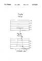
- FIGS. 4a to 4fthere is illustrated a method of making thin film transistors in accordance with the present invention.
- a metal layernamely, a chromium layer for a gate electrode is formed using a chemical vapor deposition (CVD) method.
- CVDchemical vapor deposition
- the chromium layeris then patterned to form a gate electrode 12.
- a-Si:Hamorphous silicon
- SiN xsilicon nitride
- the gate electrodemay be made of polycrystalline silicon doped with aluminum, platinum, titanium, or molybdenum.
- a photoresist 16which is subsequently subjected to a back substrate exposure causing the back side of the glass substrate 11 to be exposed to a light (for example, g-line).
- a lightfor example, g-line
- the photoresist 16is partially removed to form a photoresist pattern 16a, as shown in FIG. 4b.
- the gate electrode 12is used as a photo mask.
- the formed photoresist pattern 16amust have a width equal to the length of the gate electrode 12. However, the actual width of photoresist pattern 16a is shorter than the length of gate electrode 12, as shown in FIG. 4b.
- the width of photoresist pattern 16acan be controlled according to the exposure time and developing time of the photoresist 16. Since the photoresist 16 is exposed to the light at its portions extending inwardly from opposite side edges to positions disposed inwardly of opposite side edges of the gate electrode 12 respectively, due to the diffraction of the exposure light, there is a limitation on a reduction in the channel overlap width.
- the photoresist pattern 16ais subjected to a baking at a temperature of 120° C. to 150° C. for 10 minutes to 30 minutes so that the photoresist pattern 16a flows outwardly to make the width of photoresist pattern 16a correspond approximately to the length of gate electrode 12, as shown in FIG. 4c.
- a bakingat a temperature of 120° C. to 150° C. for 10 minutes to 30 minutes so that the photoresist pattern 16a flows outwardly to make the width of photoresist pattern 16a correspond approximately to the length of gate electrode 12, as shown in FIG. 4c.
- the contact area between the photoresist pattern 16a and the silicon nitride film 15is increased.
- the phantom lineshows the original photoresist pattern 16a and the solid line shows the photoresist pattern 16a after flowing.
- the channel overlap widthcan be reduced to 0.5 ⁇ m or less.
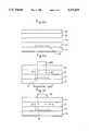
- the silicon nitride film 15 as the channel passivation layeris then etched using the photoresist pattern 16a' as a mask, to form a silicon nitride film pattern 15a. Thereafter, the photoresist pattern 16a is removed.
- the process used for etching the silicon nitride film 15is a dry etch process. As the dry etch process, a reactive ion etch process is used, for avoiding a side etching.
- N type impurity ionsfor example, phosphorous
- aceimplanted in a predetermined depth of the amorphous silicon film 14 at a density of 4 ⁇ 10 15 dose/cm 2 and an acceleration on energy of 25 Kev to 35 Kev, using the silicon nitride pattern 15a as a mask.
- N + type amorphous silicon layers 17 and 17a having a predetermined depthare formed at portions of the amorphous silicon film 14 disposed at opposite sides of the silicon nitride film pattern 15a, respectively.
- the N + type amorphous silicon layers 17 and 17aforms source and drain regions, respectively, whereas the remaining portion of amorphous silicon film 14 doped with no N + impurity ions by virtue of the silicon nitride film pattern 15a forms a channel region.
- a refractory metal layer 8 having a high meting pointis deposited using a sputtering process, to have a thickness of 100 nm, as shown in FIG. 4d.
- Chromiumis used as the material of refractory metal layer 18.
- the portions of N + type conductive layers 17 and 17abeing in contact with the refractory metal layer 18 alloy with the refractory metal layer 18 and form silicide (CrSi x ) layers 19 and 19a having a thickness of about 5 nm or less.
- an annealing processis carried out at a temperature of 250° C. to 300° C. for 30 minutes or less.
- the chromium silicide layers 19 and 19acan have a desired thickness.
- the refractory metal having a high melting pointmay include Platinum, titanium or molybdenum.
- the chromium silicide layers 19 and 19a which are formed at opposite sides of the silicon nitride film pattern 15a serving as the channel passivation layerare used as source and drain electrodes, respectively.
- source and drain regionsare formed in a self-aligned manner with respect to the gate electrode 12.
- a photoresist maskis formed at a part of the chromium layer 18 so that the chromium 18 is partially removed by using a wet etching method using a proper etchant, as shown in FIG. 4f.
- chromium patterns 18a and 18bare formed over the chromium silicide layers 19 and 19a, so as to be used as a second source electrode and a second drain electrode, respectively.
- the chromium silicide layers 19 and 19aare not etched, because of having an etch selectivity different from that of the chromium layer 18.
- a stable removal of the chromium layer 18can be achieved.
- CF 4 gas or CHF 3 gasis generally used. In this case, the gas should not contain oxygen.
- air contained an etching chambershould be sufficiently removed to maintain the etching chamber at a vacuum not more than a range of 10 -6 to 10 -7 torrs.
- the photoresist pattern which has been formed to have a width shorter than the gate length due to the diffraction of exposure lightis subjected to a baking, in accordance with the present invention, so that it flows outwardly to make the silicon nitride pattern serving as the channel passivation layer have a width approximately equal to the length of the gate electrode. Accordingly, the width of channel overlap is reduced. Furthermore, it is possible to decrease the parasitic capacitance and thus to make TFTs exhibiting higher signal-to-noise ratio, as compared with other TFT structures having the same size.
Landscapes
- Engineering & Computer Science (AREA)
- Physics & Mathematics (AREA)
- Condensed Matter Physics & Semiconductors (AREA)
- General Physics & Mathematics (AREA)
- Manufacturing & Machinery (AREA)
- Computer Hardware Design (AREA)
- Microelectronics & Electronic Packaging (AREA)
- Power Engineering (AREA)
- Thin Film Transistor (AREA)
- Liquid Crystal (AREA)
Abstract
Description
Claims (12)
Applications Claiming Priority (2)
| Application Number | Priority Date | Filing Date | Title |
|---|---|---|---|
| KR15599/1991 | 1991-09-06 | ||
| KR1019910015599AKR940007451B1 (en) | 1991-09-06 | 1991-09-06 | Method of manufacturing thin film transistor |
Publications (1)
| Publication Number | Publication Date |
|---|---|
| US5371025Atrue US5371025A (en) | 1994-12-06 |
Family
ID=19319678
Family Applications (1)
| Application Number | Title | Priority Date | Filing Date |
|---|---|---|---|
| US07/940,060Expired - LifetimeUS5371025A (en) | 1991-09-06 | 1992-09-03 | Method of making thin film transistors |
Country Status (3)
| Country | Link |
|---|---|
| US (1) | US5371025A (en) |
| JP (1) | JPH0828523B2 (en) |
| KR (1) | KR940007451B1 (en) |
Cited By (36)
| Publication number | Priority date | Publication date | Assignee | Title |
|---|---|---|---|---|
| US5468662A (en)* | 1992-10-02 | 1995-11-21 | Texas Instruments Incorporated | Method of making thin film transistor and a silicide local interconnect |
| US5477355A (en)* | 1992-01-28 | 1995-12-19 | Hitachi, Ltd. | Process for producing the passivation layer of an active matrix substrate by back exposure |
| US5610082A (en)* | 1992-12-29 | 1997-03-11 | Lg Electronics Inc. | Method for fabricating thin film transistor using back light exposure |
| US5612235A (en)* | 1995-11-01 | 1997-03-18 | Industrial Technology Research Institute | Method of making thin film transistor with light-absorbing layer |
| US5618384A (en)* | 1995-12-27 | 1997-04-08 | Chartered Semiconductor Manufacturing Pte, Ltd. | Method for forming residue free patterned conductor layers upon high step height integrated circuit substrates using reflow of photoresist |
| US5656523A (en)* | 1994-02-16 | 1997-08-12 | Micron Technology, Inc. | Photoresist flow during the formation of a semiconductor device |
| US5656824A (en)* | 1995-06-02 | 1997-08-12 | Ois Optical Imaging Systems, Inc. | TFT with reduced channel length and method of making same |
| EP0780892A3 (en)* | 1995-12-22 | 1997-10-15 | Xerox Corp | Method of manufacturing an inverted thin film transistor |
| US5702960A (en)* | 1994-02-25 | 1997-12-30 | Samsung Electronics Co., Ltd. | Method for manufacturing polysilicon thin film transistor |
| US5719078A (en)* | 1995-02-11 | 1998-02-17 | Samsung Electronics Co., Ltd. | Method for making a thin film transistor panel used in a liquid crystal display having a completely self-aligned thin film transistor |
| US5751381A (en)* | 1993-12-21 | 1998-05-12 | Hitachi, Ltd. | Active matrix LCD device with image signal lines having a multilayered structure |
| EP0766296A3 (en)* | 1995-09-29 | 1998-05-13 | Sony Corporation | Method of manufacturing a thin film transistor |
| US5792708A (en)* | 1996-03-06 | 1998-08-11 | Chartered Semiconductor Manufacturing Pte Ltd. | Method for forming residue free patterned polysilicon layers upon high step height integrated circuit substrates |
| KR100237709B1 (en)* | 1995-08-31 | 2000-01-15 | 니시무로 타이죠 | Manufacturing method of thin-film transistor |
| US20020025591A1 (en)* | 2000-08-11 | 2002-02-28 | Hideto Ohnuma | Method of manufacturing a semiconductor device |
| US6391693B1 (en)* | 1998-06-25 | 2002-05-21 | Hyundai Display Technology Inc. | Method for making polysilicon thin film transistor having multiple gate electrodes |
| WO2002091455A1 (en)* | 2001-05-10 | 2002-11-14 | Koninklijke Philips Electronics N.V. | Thin film transistor self-aligned to a light-shield layer |
| US6562670B2 (en)* | 2001-02-02 | 2003-05-13 | Hannstar Display Corporation | Poly-silicon thin film transistor and method for fabricating thereof |
| US20030141507A1 (en)* | 2002-01-28 | 2003-07-31 | Krames Michael R. | LED efficiency using photonic crystal structure |
| US20040126941A1 (en)* | 2002-05-06 | 2004-07-01 | Teizo Yukawa | Thin film transistor self-aligned to a light-shield layer |
| US20050082545A1 (en)* | 2003-10-21 | 2005-04-21 | Wierer Jonathan J.Jr. | Photonic crystal light emitting device |
| EP1467415A3 (en)* | 2003-04-08 | 2005-06-15 | LumiLeds Lighting U.S., LLC | Improved LED efficiency using photonic crystal structure |
| WO2005071753A1 (en)* | 2004-01-24 | 2005-08-04 | Koninklijke Philips Electronics N.V. | Transistor manufacture |
| US20050205883A1 (en)* | 2004-03-19 | 2005-09-22 | Wierer Jonathan J Jr | Photonic crystal light emitting device |
| US20060027815A1 (en)* | 2004-08-04 | 2006-02-09 | Wierer Jonathan J Jr | Photonic crystal light emitting device with multiple lattices |
| US20060079042A1 (en)* | 2004-09-24 | 2006-04-13 | Lg Philips Lcd Co., Ltd. | Thin film transistor and manufacturing method thereof |
| US20060216872A1 (en)* | 2005-03-24 | 2006-09-28 | Tadashi Arai | Method of manufacturing a semiconductor device having an organic thin film transistor |
| US20060240606A1 (en)* | 2005-04-26 | 2006-10-26 | Nec Lcd Technologies, Ltd. | Method of manufacturing a liquid crystal display device |
| US20060261336A1 (en)* | 2005-05-20 | 2006-11-23 | Semiconductor Energy Laboratory Co., Ltd. | Semiconductor device and manufacturing method thereof |
| US20060278875A1 (en)* | 2005-06-10 | 2006-12-14 | Semiconductor Energy Laboratory Co., Ltd. | Semiconductor device and manufacturing method thereof |
| US20060284187A1 (en)* | 2005-06-17 | 2006-12-21 | Lumileds Lighting U.S, Llc | Grown photonic crystals in semiconductor light emitting devices |
| US20070022852A1 (en)* | 2005-09-09 | 2007-02-01 | Tracy Jack R | Retractor for circular saw lower safety-guard |
| US20070037070A1 (en)* | 2005-08-12 | 2007-02-15 | Semiconductor Energy Laboratory Co., Ltd. | Light exposure mask and method for manufacturing semiconductor device using the same |
| US20070037069A1 (en)* | 2005-08-12 | 2007-02-15 | Semiconductor Energy Laboratory Co., Ltd. | Exposure mask |
| US20080206911A1 (en)* | 2007-02-22 | 2008-08-28 | Samsung Electronics Co., Ltd. | Method of manufacturing liquid crystal display |
| CN105742240A (en)* | 2016-04-05 | 2016-07-06 | 武汉华星光电技术有限公司 | Fabrication method of low temperature poly-silicon (LTPS) array substrate |
Families Citing this family (1)
| Publication number | Priority date | Publication date | Assignee | Title |
|---|---|---|---|---|
| US5943559A (en)* | 1997-06-23 | 1999-08-24 | Nec Corporation | Method for manufacturing liquid crystal display apparatus with drain/source silicide electrodes made by sputtering process |
Citations (2)
| Publication number | Priority date | Publication date | Assignee | Title |
|---|---|---|---|---|
| US5010027A (en)* | 1990-03-21 | 1991-04-23 | General Electric Company | Method for fabricating a self-aligned thin-film transistor utilizing planarization and back-side photoresist exposure |
| US5130263A (en)* | 1990-04-17 | 1992-07-14 | General Electric Company | Method for photolithographically forming a selfaligned mask using back-side exposure and a non-specular reflecting layer |
- 1991
- 1991-09-06KRKR1019910015599Apatent/KR940007451B1/ennot_activeExpired - Fee Related
- 1992
- 1992-09-03USUS07/940,060patent/US5371025A/ennot_activeExpired - Lifetime
- 1992-09-04JPJP26059792Apatent/JPH0828523B2/ennot_activeExpired - Fee Related
Patent Citations (2)
| Publication number | Priority date | Publication date | Assignee | Title |
|---|---|---|---|---|
| US5010027A (en)* | 1990-03-21 | 1991-04-23 | General Electric Company | Method for fabricating a self-aligned thin-film transistor utilizing planarization and back-side photoresist exposure |
| US5130263A (en)* | 1990-04-17 | 1992-07-14 | General Electric Company | Method for photolithographically forming a selfaligned mask using back-side exposure and a non-specular reflecting layer |
Non-Patent Citations (2)
| Title |
|---|
| Nishida et al., A New Self Aligned A Si TFT Using Ion Doping And Chromium Silicide Formation, Material Research Society Symp. Proc., vol. 219, pp. 303 308, 1991 (Exhibit 1).* |
| Nishida et al., A New Self-Aligned A-Si TFT Using Ion Doping And Chromium Silicide Formation, Material Research Society Symp. Proc., vol. 219, pp. 303-308, 1991 (Exhibit 1). |
Cited By (75)
| Publication number | Priority date | Publication date | Assignee | Title |
|---|---|---|---|---|
| US5477355A (en)* | 1992-01-28 | 1995-12-19 | Hitachi, Ltd. | Process for producing the passivation layer of an active matrix substrate by back exposure |
| US5468662A (en)* | 1992-10-02 | 1995-11-21 | Texas Instruments Incorporated | Method of making thin film transistor and a silicide local interconnect |
| US5610082A (en)* | 1992-12-29 | 1997-03-11 | Lg Electronics Inc. | Method for fabricating thin film transistor using back light exposure |
| USRE39798E1 (en)* | 1993-12-21 | 2007-08-28 | Hitachi, Ltd. | Active matrix LCD device with image signal lines having a multilayered structure |
| US5751381A (en)* | 1993-12-21 | 1998-05-12 | Hitachi, Ltd. | Active matrix LCD device with image signal lines having a multilayered structure |
| US5656523A (en)* | 1994-02-16 | 1997-08-12 | Micron Technology, Inc. | Photoresist flow during the formation of a semiconductor device |
| US5702960A (en)* | 1994-02-25 | 1997-12-30 | Samsung Electronics Co., Ltd. | Method for manufacturing polysilicon thin film transistor |
| US5719078A (en)* | 1995-02-11 | 1998-02-17 | Samsung Electronics Co., Ltd. | Method for making a thin film transistor panel used in a liquid crystal display having a completely self-aligned thin film transistor |
| US5656824A (en)* | 1995-06-02 | 1997-08-12 | Ois Optical Imaging Systems, Inc. | TFT with reduced channel length and method of making same |
| KR100237709B1 (en)* | 1995-08-31 | 2000-01-15 | 니시무로 타이죠 | Manufacturing method of thin-film transistor |
| EP0766296A3 (en)* | 1995-09-29 | 1998-05-13 | Sony Corporation | Method of manufacturing a thin film transistor |
| US5612235A (en)* | 1995-11-01 | 1997-03-18 | Industrial Technology Research Institute | Method of making thin film transistor with light-absorbing layer |
| EP0780892A3 (en)* | 1995-12-22 | 1997-10-15 | Xerox Corp | Method of manufacturing an inverted thin film transistor |
| US5618384A (en)* | 1995-12-27 | 1997-04-08 | Chartered Semiconductor Manufacturing Pte, Ltd. | Method for forming residue free patterned conductor layers upon high step height integrated circuit substrates using reflow of photoresist |
| US5792708A (en)* | 1996-03-06 | 1998-08-11 | Chartered Semiconductor Manufacturing Pte Ltd. | Method for forming residue free patterned polysilicon layers upon high step height integrated circuit substrates |
| US6391693B1 (en)* | 1998-06-25 | 2002-05-21 | Hyundai Display Technology Inc. | Method for making polysilicon thin film transistor having multiple gate electrodes |
| US20020025591A1 (en)* | 2000-08-11 | 2002-02-28 | Hideto Ohnuma | Method of manufacturing a semiconductor device |
| US7169656B2 (en) | 2000-08-11 | 2007-01-30 | Semiconductor Energy Laboratory Co., Ltd. | Method of manufacturing a semiconductor device |
| US8324032B2 (en) | 2000-08-11 | 2012-12-04 | Semiconductor Energy Laboratory Co., Ltd. | Method of manufacturing a semiconductor device |
| US7955912B2 (en) | 2000-08-11 | 2011-06-07 | Semiconductor Energy Laboratory Co., Ltd. | Method of manufacturing a semiconductor device |
| US7745271B2 (en) | 2000-08-11 | 2010-06-29 | Semiconductor Energy Laboratory Co., Ltd. | Method of manufacturing a semiconductor device |
| US20100261320A1 (en)* | 2000-08-11 | 2010-10-14 | Semiconductor Energy Laboratory Co., Ltd. | Method of manufacturing a semiconductor device |
| US7223643B2 (en)* | 2000-08-11 | 2007-05-29 | Semiconductor Energy Laboratory Co., Ltd. | Method of manufacturing a semiconductor device |
| US20060014335A1 (en)* | 2000-08-11 | 2006-01-19 | Semiconductor Energy Laboratory Co., Ltd. | Method of manufacturing a semiconductor device |
| US20080119024A1 (en)* | 2000-08-11 | 2008-05-22 | Semiconductor Energy Laboratory Co., Ltd. | Method of manufacturing a semiconductor device |
| US20070218604A1 (en)* | 2000-08-11 | 2007-09-20 | Semiconductor Energy Laboratory Co., Ltd. | Method of manufacturing a semiconductor device |
| US7316946B2 (en) | 2000-08-11 | 2008-01-08 | Semiconductor Energy Laboratory Co., Ltd. | Method of manufacturing a semiconductor device |
| US6562670B2 (en)* | 2001-02-02 | 2003-05-13 | Hannstar Display Corporation | Poly-silicon thin film transistor and method for fabricating thereof |
| WO2002091455A1 (en)* | 2001-05-10 | 2002-11-14 | Koninklijke Philips Electronics N.V. | Thin film transistor self-aligned to a light-shield layer |
| US20030141507A1 (en)* | 2002-01-28 | 2003-07-31 | Krames Michael R. | LED efficiency using photonic crystal structure |
| US7279718B2 (en) | 2002-01-28 | 2007-10-09 | Philips Lumileds Lighting Company, Llc | LED including photonic crystal structure |
| US20080070334A1 (en)* | 2002-01-28 | 2008-03-20 | Philips Lumileds Lighting Company, Llc | LED Including Photonic Crystal Structure |
| US7642108B2 (en) | 2002-01-28 | 2010-01-05 | Philips Lumileds Lighting Company, Llc | LED including photonic crystal structure |
| US6972219B2 (en)* | 2002-05-06 | 2005-12-06 | Koninklijke Philips Electronics N.V. | Thin film transistor self-aligned to a light-shield layer |
| US20040126941A1 (en)* | 2002-05-06 | 2004-07-01 | Teizo Yukawa | Thin film transistor self-aligned to a light-shield layer |
| EP1467415A3 (en)* | 2003-04-08 | 2005-06-15 | LumiLeds Lighting U.S., LLC | Improved LED efficiency using photonic crystal structure |
| US7294862B2 (en) | 2003-10-21 | 2007-11-13 | Philips Lumileds Lighting Company, Llc | Photonic crystal light emitting device |
| US20060151794A1 (en)* | 2003-10-21 | 2006-07-13 | Wierer Jonathan J Jr | Photonic crystal light emitting device |
| US20050082545A1 (en)* | 2003-10-21 | 2005-04-21 | Wierer Jonathan J.Jr. | Photonic crystal light emitting device |
| US7012279B2 (en) | 2003-10-21 | 2006-03-14 | Lumileds Lighting U.S., Llc | Photonic crystal light emitting device |
| WO2005071753A1 (en)* | 2004-01-24 | 2005-08-04 | Koninklijke Philips Electronics N.V. | Transistor manufacture |
| US20060163606A1 (en)* | 2004-03-19 | 2006-07-27 | Wierer Jonathan J Jr | Photonic crystal light emitting device |
| US20050205883A1 (en)* | 2004-03-19 | 2005-09-22 | Wierer Jonathan J Jr | Photonic crystal light emitting device |
| US7675084B2 (en) | 2004-03-19 | 2010-03-09 | Philips Lumileds Lighting Co, LLC | Photonic crystal light emitting device |
| US20090045427A1 (en)* | 2004-03-19 | 2009-02-19 | Philips Lumileds Lighting Company, Llc | Photonic Crystal Light Emitting Device |
| US7442965B2 (en) | 2004-03-19 | 2008-10-28 | Philips Lumileds Lighting Company, Llc | Photonic crystal light emitting device |
| US20060027815A1 (en)* | 2004-08-04 | 2006-02-09 | Wierer Jonathan J Jr | Photonic crystal light emitting device with multiple lattices |
| US7442964B2 (en) | 2004-08-04 | 2008-10-28 | Philips Lumileds Lighting Company, Llc | Photonic crystal light emitting device with multiple lattices |
| US20060079042A1 (en)* | 2004-09-24 | 2006-04-13 | Lg Philips Lcd Co., Ltd. | Thin film transistor and manufacturing method thereof |
| US7332382B2 (en)* | 2004-09-24 | 2008-02-19 | Lg. Philips Lcd. Co., Ltd | Thin film transistor and manufacturing method thereof |
| US20060216872A1 (en)* | 2005-03-24 | 2006-09-28 | Tadashi Arai | Method of manufacturing a semiconductor device having an organic thin film transistor |
| US7300828B2 (en)* | 2005-04-26 | 2007-11-27 | Nec Lcd Technologies. Ltd. | Method of manufacturing a liquid crystal display device |
| US20060240606A1 (en)* | 2005-04-26 | 2006-10-26 | Nec Lcd Technologies, Ltd. | Method of manufacturing a liquid crystal display device |
| US20060261336A1 (en)* | 2005-05-20 | 2006-11-23 | Semiconductor Energy Laboratory Co., Ltd. | Semiconductor device and manufacturing method thereof |
| US7947538B2 (en) | 2005-05-20 | 2011-05-24 | Semiconductor Energy Laboratory Co., Ltd. | Semiconductor device and manufacturing method thereof |
| US7579220B2 (en) | 2005-05-20 | 2009-08-25 | Semiconductor Energy Laboratory Co., Ltd. | Semiconductor device manufacturing method |
| US20090291536A1 (en)* | 2005-05-20 | 2009-11-26 | Semiconductor Energy Laboratory Co., Ltd. | Semiconductor device and manufacturing method thereof |
| US20060278875A1 (en)* | 2005-06-10 | 2006-12-14 | Semiconductor Energy Laboratory Co., Ltd. | Semiconductor device and manufacturing method thereof |
| US7588970B2 (en) | 2005-06-10 | 2009-09-15 | Semiconductor Energy Laboratory Co., Ltd. | Semiconductor device and manufacturing method thereof |
| US8043902B2 (en) | 2005-06-10 | 2011-10-25 | Semiconductor Energy Laboratory Co., Ltd. | Semiconductor device and manufacturing method thereof |
| US20100015764A1 (en)* | 2005-06-10 | 2010-01-21 | Semiconductor Energy Laboratory Co., Ltd. | Semiconductor device and manufacturing method thereof |
| US20060284187A1 (en)* | 2005-06-17 | 2006-12-21 | Lumileds Lighting U.S, Llc | Grown photonic crystals in semiconductor light emitting devices |
| US8163575B2 (en) | 2005-06-17 | 2012-04-24 | Philips Lumileds Lighting Company Llc | Grown photonic crystals in semiconductor light emitting devices |
| US9000450B2 (en) | 2005-06-17 | 2015-04-07 | Philips Lumileds Lighting Company Llc | Grown photonic crystals in semiconductor light emitting devices |
| US20070037070A1 (en)* | 2005-08-12 | 2007-02-15 | Semiconductor Energy Laboratory Co., Ltd. | Light exposure mask and method for manufacturing semiconductor device using the same |
| US20070037069A1 (en)* | 2005-08-12 | 2007-02-15 | Semiconductor Energy Laboratory Co., Ltd. | Exposure mask |
| US20110170084A1 (en)* | 2005-08-12 | 2011-07-14 | Semiconductor Energy Laboratory Co., Ltd. | Light exposure mask and method for manufacturing semiconductor device using the same |
| US20090176073A1 (en)* | 2005-08-12 | 2009-07-09 | Semiconductor Energy Laboratory Co., Ltd. | Exposure mask |
| US7914971B2 (en) | 2005-08-12 | 2011-03-29 | Semiconductor Energy Laboratory Co., Ltd. | Light exposure mask and method for manufacturing semiconductor device using the same |
| US7524593B2 (en) | 2005-08-12 | 2009-04-28 | Semiconductor Energy Laboratory Co., Ltd. | Exposure mask |
| US20070022852A1 (en)* | 2005-09-09 | 2007-02-01 | Tracy Jack R | Retractor for circular saw lower safety-guard |
| US20080206911A1 (en)* | 2007-02-22 | 2008-08-28 | Samsung Electronics Co., Ltd. | Method of manufacturing liquid crystal display |
| CN105742240A (en)* | 2016-04-05 | 2016-07-06 | 武汉华星光电技术有限公司 | Fabrication method of low temperature poly-silicon (LTPS) array substrate |
| US10157940B2 (en) | 2016-04-05 | 2018-12-18 | Wuhan China Star Optoelectronics Technology Co., Ltd. | Method for manufacturing LTPS array substrate |
| CN105742240B (en)* | 2016-04-05 | 2019-09-13 | 武汉华星光电技术有限公司 | A kind of manufacturing method of LTPS array substrate |
Also Published As
| Publication number | Publication date |
|---|---|
| JPH0828523B2 (en) | 1996-03-21 |
| JPH05235034A (en) | 1993-09-10 |
| KR940007451B1 (en) | 1994-08-18 |
Similar Documents
| Publication | Publication Date | Title |
|---|---|---|
| US5371025A (en) | Method of making thin film transistors | |
| US5532180A (en) | Method of fabricating a TFT with reduced channel length | |
| US6504182B2 (en) | Thin-film transistors | |
| US6320224B1 (en) | Method for producing a semiconductor integrated circuit including a thin film transistor and a capacitor | |
| US6537843B2 (en) | Thin film transistor and method of manufacturing the same | |
| KR100229676B1 (en) | Manufacturing method of self-align thin film transistor | |
| JP2011023740A (en) | Method for forming amorphous silicon thin film transistor on surface of substrate | |
| JP3086579B2 (en) | Method for manufacturing thin film transistor | |
| KR20020021546A (en) | Poly-Si Thin Film Transistor Having Back Bias Effects and Fabrication Method Thereof | |
| JP2739642B2 (en) | Thin film transistor and method of manufacturing the same | |
| JP2011023741A (en) | Array | |
| US6124153A (en) | Method for manufacturing a polysilicon TFT with a variable thickness gate oxide | |
| US5920362A (en) | Method of forming thin-film transistor liquid crystal display having a silicon active layer contacting a sidewall of a data line and a storage capacitor electrode | |
| US5384271A (en) | Method for reduction of off-current in thin film transistors | |
| US5306653A (en) | Method of making thin film transistors | |
| US5347146A (en) | Polysilicon thin film transistor of a liquid crystal display | |
| KR20050052475A (en) | Thin film transistor | |
| US6656776B2 (en) | Thin film transistor and fabricating method thereof | |
| JP2621619B2 (en) | Method for manufacturing thin film transistor | |
| KR100370451B1 (en) | Method for manufacturing amorphous silicon thin film transistor and liquid crystal display using simple process | |
| KR100254924B1 (en) | Manufacturing Method of Image Display Device | |
| KR100304911B1 (en) | Thin Film Transistor Manufacturing Method | |
| KR100303710B1 (en) | Amorphous Silicon Thin Film Transistor and Liquid Crystal Display Device Structure and Manufacturing Method | |
| JP2603247B2 (en) | Thin film transistor | |
| JP2002523898A (en) | Thin film transistor and method of manufacturing the same |
Legal Events
| Date | Code | Title | Description |
|---|---|---|---|
| AS | Assignment | Owner name:GOLD STAR CO. LTD., KOREA, REPUBLIC OF Free format text:ASSIGNMENT OF ASSIGNORS INTEREST.;ASSIGNOR:SUNG, KANG H.;REEL/FRAME:006294/0761 Effective date:19920921 | |
| STCF | Information on status: patent grant | Free format text:PATENTED CASE | |
| FEPP | Fee payment procedure | Free format text:PAYOR NUMBER ASSIGNED (ORIGINAL EVENT CODE: ASPN); ENTITY STATUS OF PATENT OWNER: LARGE ENTITY | |
| FPAY | Fee payment | Year of fee payment:4 | |
| AS | Assignment | Owner name:LG. PHILIPS LCD CO., LTD., KOREA, DEMOCRATIC PEOPL Free format text:ASSIGNMENT OF ASSIGNORS INTEREST;ASSIGNOR:LG ELECTRONICS, INC.;REEL/FRAME:010281/0291 Effective date:19990921 | |
| FPAY | Fee payment | Year of fee payment:8 | |
| FPAY | Fee payment | Year of fee payment:12 | |
| AS | Assignment | Owner name:LG.PHILIPS LCD CO., LTD., KOREA, REPUBLIC OF Free format text:ASSIGNMENT OF ASSIGNORS INTEREST;ASSIGNOR:LG ELECTRONICS INC.;REEL/FRAME:020385/0124 Effective date:19990921 | |
| AS | Assignment | Owner name:LG DISPLAY CO., LTD., KOREA, REPUBLIC OF Free format text:CHANGE OF NAME;ASSIGNOR:LG.PHILIPS LCD CO., LTD.;REEL/FRAME:021890/0892 Effective date:20080304 |