US5370765A - Electron cyclotron resonance plasma source and method of operation - Google Patents
Electron cyclotron resonance plasma source and method of operationDownload PDFInfo
- Publication number
- US5370765A US5370765AUS08/048,744US4874493AUS5370765AUS 5370765 AUS5370765 AUS 5370765AUS 4874493 AUS4874493 AUS 4874493AUS 5370765 AUS5370765 AUS 5370765A
- Authority
- US
- United States
- Prior art keywords
- chamber
- plasma
- magnetic field
- specimen
- ecr
- Prior art date
- Legal status (The legal status is an assumption and is not a legal conclusion. Google has not performed a legal analysis and makes no representation as to the accuracy of the status listed.)
- Expired - Lifetime
Links
- 238000000034methodMethods0.000titleclaimsabstractdescription31
- 238000010438heat treatmentMethods0.000claimsabstractdescription15
- 238000004891communicationMethods0.000claimsabstractdescription13
- 238000005229chemical vapour depositionMethods0.000claimsabstractdescription10
- 238000003486chemical etchingMethods0.000claimsabstractdescription9
- 230000003993interactionEffects0.000claimsdescription27
- 238000000429assemblyMethods0.000claimsdescription19
- 230000000712assemblyEffects0.000claimsdescription19
- 239000002245particleSubstances0.000claimsdescription18
- 239000012535impuritySubstances0.000claimsdescription12
- 230000008569processEffects0.000claimsdescription11
- VYPSYNLAJGMNEJ-UHFFFAOYSA-NSilicium dioxideChemical compoundO=[Si]=OVYPSYNLAJGMNEJ-UHFFFAOYSA-N0.000claimsdescription9
- 239000005350fused silica glassSubstances0.000claimsdescription8
- 238000002347injectionMethods0.000claimsdescription7
- 239000007924injectionSubstances0.000claimsdescription7
- 230000005670electromagnetic radiationEffects0.000claimsdescription6
- 238000004381surface treatmentMethods0.000claims3
- 229910000831SteelInorganic materials0.000claims1
- 239000010959steelSubstances0.000claims1
- 238000009826distributionMethods0.000abstractdescription3
- 210000002381plasmaAnatomy0.000description140
- 239000007789gasSubstances0.000description29
- 150000002500ionsChemical class0.000description29
- 230000005495cold plasmaEffects0.000description10
- 230000006870functionEffects0.000description8
- 238000012545processingMethods0.000description8
- 238000000151depositionMethods0.000description6
- 230000004927fusionEffects0.000description6
- 230000007935neutral effectEffects0.000description6
- 239000000376reactantSubstances0.000description6
- 241000894007speciesSpecies0.000description6
- 238000003491arrayMethods0.000description5
- 230000008021depositionEffects0.000description5
- 238000013461designMethods0.000description5
- 239000000463materialSubstances0.000description5
- 229910052751metalInorganic materials0.000description5
- 239000002184metalSubstances0.000description5
- 239000000203mixtureSubstances0.000description5
- 229910001209Low-carbon steelInorganic materials0.000description4
- 230000008901benefitEffects0.000description4
- 230000015556catabolic processEffects0.000description4
- 238000005530etchingMethods0.000description4
- 230000004907fluxEffects0.000description4
- 230000007246mechanismEffects0.000description4
- 239000004065semiconductorSubstances0.000description4
- 230000007723transport mechanismEffects0.000description4
- 235000012431wafersNutrition0.000description4
- 230000015572biosynthetic processEffects0.000description3
- 230000003247decreasing effectEffects0.000description3
- 238000005516engineering processMethods0.000description3
- 238000004519manufacturing processMethods0.000description3
- 239000000758substrateSubstances0.000description3
- PXHVJJICTQNCMI-UHFFFAOYSA-NNickelChemical compound[Ni]PXHVJJICTQNCMI-UHFFFAOYSA-N0.000description2
- 238000013459approachMethods0.000description2
- 238000006243chemical reactionMethods0.000description2
- 238000006073displacement reactionMethods0.000description2
- 238000011156evaluationMethods0.000description2
- 239000012530fluidSubstances0.000description2
- 230000004048modificationEffects0.000description2
- 238000012986modificationMethods0.000description2
- 230000005855radiationEffects0.000description2
- 238000004544sputter depositionMethods0.000description2
- 238000012546transferMethods0.000description2
- 238000007792additionMethods0.000description1
- 229910052782aluminiumInorganic materials0.000description1
- XAGFODPZIPBFFR-UHFFFAOYSA-NaluminiumChemical compound[Al]XAGFODPZIPBFFR-UHFFFAOYSA-N0.000description1
- 230000001668ameliorated effectEffects0.000description1
- 230000009286beneficial effectEffects0.000description1
- 230000008859changeEffects0.000description1
- 238000010276constructionMethods0.000description1
- 230000008878couplingEffects0.000description1
- 238000010168coupling processMethods0.000description1
- 238000005859coupling reactionMethods0.000description1
- 230000007423decreaseEffects0.000description1
- 230000001419dependent effectEffects0.000description1
- 238000011161developmentMethods0.000description1
- 230000018109developmental processEffects0.000description1
- 239000010432diamondSubstances0.000description1
- 229910003460diamondInorganic materials0.000description1
- 239000003989dielectric materialSubstances0.000description1
- 230000000694effectsEffects0.000description1
- 238000001803electron scatteringMethods0.000description1
- 230000003628erosive effectEffects0.000description1
- 238000002474experimental methodMethods0.000description1
- 230000012447hatchingEffects0.000description1
- 239000002784hot electronSubstances0.000description1
- 238000005286illuminationMethods0.000description1
- 239000011261inert gasSubstances0.000description1
- 238000009413insulationMethods0.000description1
- 238000005468ion implantationMethods0.000description1
- 239000000696magnetic materialSubstances0.000description1
- 230000005405multipoleEffects0.000description1
- 229910052759nickelInorganic materials0.000description1
- 230000000149penetrating effectEffects0.000description1
- 230000035515penetrationEffects0.000description1
- 238000001020plasma etchingMethods0.000description1
- 238000000623plasma-assisted chemical vapour depositionMethods0.000description1
- 230000002265preventionEffects0.000description1
- 239000010453quartzSubstances0.000description1
- 230000009467reductionEffects0.000description1
- 230000002040relaxant effectEffects0.000description1
- 229910001220stainless steelInorganic materials0.000description1
- 239000010935stainless steelSubstances0.000description1
- 230000007704transitionEffects0.000description1
- 238000007740vapor depositionMethods0.000description1
Images


Classifications
- H—ELECTRICITY
- H05—ELECTRIC TECHNIQUES NOT OTHERWISE PROVIDED FOR
- H05H—PLASMA TECHNIQUE; PRODUCTION OF ACCELERATED ELECTRICALLY-CHARGED PARTICLES OR OF NEUTRONS; PRODUCTION OR ACCELERATION OF NEUTRAL MOLECULAR OR ATOMIC BEAMS
- H05H1/00—Generating plasma; Handling plasma
- H05H1/02—Arrangements for confining plasma by electric or magnetic fields; Arrangements for heating plasma
- H05H1/16—Arrangements for confining plasma by electric or magnetic fields; Arrangements for heating plasma using externally-applied electric and magnetic fields
- H05H1/18—Arrangements for confining plasma by electric or magnetic fields; Arrangements for heating plasma using externally-applied electric and magnetic fields wherein the fields oscillate at very high frequency, e.g. in the microwave range, e.g. using cyclotron resonance
- H—ELECTRICITY
- H01—ELECTRIC ELEMENTS
- H01J—ELECTRIC DISCHARGE TUBES OR DISCHARGE LAMPS
- H01J37/00—Discharge tubes with provision for introducing objects or material to be exposed to the discharge, e.g. for the purpose of examination or processing thereof
- H01J37/32—Gas-filled discharge tubes
- H01J37/32009—Arrangements for generation of plasma specially adapted for examination or treatment of objects, e.g. plasma sources
- H01J37/32192—Microwave generated discharge
- H01J37/32211—Means for coupling power to the plasma
- H01J37/32229—Waveguides
- H—ELECTRICITY
- H01—ELECTRIC ELEMENTS
- H01J—ELECTRIC DISCHARGE TUBES OR DISCHARGE LAMPS
- H01J37/00—Discharge tubes with provision for introducing objects or material to be exposed to the discharge, e.g. for the purpose of examination or processing thereof
- H01J37/32—Gas-filled discharge tubes
- H01J37/32431—Constructional details of the reactor
- H01J37/3266—Magnetic control means
- H01J37/32678—Electron cyclotron resonance
- H—ELECTRICITY
- H01—ELECTRIC ELEMENTS
- H01J—ELECTRIC DISCHARGE TUBES OR DISCHARGE LAMPS
- H01J2237/00—Discharge tubes exposing object to beam, e.g. for analysis treatment, etching, imaging
- H01J2237/32—Processing objects by plasma generation
- H01J2237/33—Processing objects by plasma generation characterised by the type of processing
- H01J2237/332—Coating
- H01J2237/3322—Problems associated with coating
- H01J2237/3323—Problems associated with coating uniformity
- H—ELECTRICITY
- H01—ELECTRIC ELEMENTS
- H01J—ELECTRIC DISCHARGE TUBES OR DISCHARGE LAMPS
- H01J2237/00—Discharge tubes exposing object to beam, e.g. for analysis treatment, etching, imaging
- H01J2237/32—Processing objects by plasma generation
- H01J2237/33—Processing objects by plasma generation characterised by the type of processing
- H01J2237/334—Etching
- H01J2237/3343—Problems associated with etching
- H01J2237/3345—Problems associated with etching anisotropy
Definitions
- the present inventionrelates to a method and apparatus employing electron cyclotron resonance heating for producing a plasma stream and more particularly to a method and apparatus employing such a plasma source for use in applications such as a negative ion source or the treatment of specimens such as VLSI wafers by applications including chemical vapor deposition and etching carried out by means of the plasma stream.
- the present inventionis based upon generation of cold plasma by electron cyclotron resonance heating in order to develop various desired characteristics within the plasma.
- the present invention and related prior artare based upon criteria where conditions governing steady-state values of plasma density and composition as well as the electron and ion temperatures are determined by microwave power and neutral gas pressure through the conditions for particle and power balances for each of three coupled species; namely electrons, ions and gas atoms.
- plasma sources employing electron cyclotron resonance (ECR) heatingcomprise an emerging or developing technology, for example in the deposition and etching of VLSI films.
- ECRelectron cyclotron resonance
- Such applicationsare typical of other processing technologies requiring the capability of achieving submicron feature dimensions, substantial processing rates and the capability of uniformly processing large specimens such as wafers.
- the general characteristics of these technologiesare believed to be well understood by those skilled in the art and are accordingly not discussed in substantial detail herein.
- ECR plasma source of the present inventionis contemplated for use in vapor deposition or etching applications, the general parameters of those applications are not of themselves a portion of the invention. Certain considerations in such applications are briefly summarized below in order to facilitate a more complete understanding of the invention.
- ECR plasma sourcessuch as those provided by the present invention and the prior art discussed below employ magnetic fields and microwave power to create chemically active plasmas, preferably at very low gas pressures.
- Low pressure operationis desirable in order to permit the formation of highly directional or anisotropic streams of low-temperature ions, radicals and other species of reactants which are uniform over substantial transverse dimensions larger than the sample being processed.
- a reactant gasis introduced into an evacuated chamber which is immersed in a steady magnetic field and exposed to electromagnetic radiation.
- the frequency of the radiation, f.sub. ⁇is selected to resonate with the electron gyrofrequency in a region of the steady magnetic field called the resonant interaction region.
- Electrons in the resonant interaction regiongain kinetic energy from the electromagnetic radiation, and if the radiation power and the gas pressure are suitably adjusted, the heated electrons may ionize the reactant gas molecules to create a plasma.
- the plasma ions and electronsflow out of the resonant interaction region and impinge on the VLSI film where the ions can be used for deposition of new materials or etching of existing films. If the plasma density is sufficiently high, the deposition or etch rates can be rapid, and if the ion and electron energies are sufficiently low, damage to the sample being processed can be prevented.
- it is necessary for the ion trajectoriesit is necessary for the ion trajectories to be highly directional. This is made possible by operating at sufficiently low gas pressures to ensure that the ion mean-free-path for scattering is longer than the distance to the specimens.
- the substratecan be biased electrically, relative to the plasma interior, to potentials of sufficient magnitude to insure highly anisotropic processing without exceeding a threshold ion energy above which excessive damage may occur.
- the stream of plasma from the ECR sourcebe uniform over transverse dimensions larger than 15-20 cm.
- the present inventionaddresses the need for large, uniform streams of low-temperature plasmas with high densities of ions and electrons in low-pressure neutral gas mixtures.
- Sumitomo sourceIn the prior art, one class of ECR plasma sources is generally referred to as the "Sumitomo source".
- the Sumitomo sourceis illustrated for example by the plasma deposition apparatus of Matsuo, et al. U.S. Pat. No. 4,401,054 issued Aug. 30, 1983, and further discussed in S. Matsuo, M. Kiuchi and T. Ono, in Proceedings of the Tenth Symposium on IISIAT 1986, Tokyo, p. 471 and T. Ono, M. Oda, C. Takahashi and S. Matsuo, J. Vac. Sci. Technol. B4, 696 (1986).
- plasma-enhanced processing applicationsrequire that the plasma be enclosed in chambers whose walls are made of particular materials, such as fused quartz, stainless steel, nickel, aluminum, etc., depending on the specific requirements of the process for which the plasma is to be employed.
- a plasma source chamberis formed as a symmetrical cylinder having a longitudinal axis with an outlet at one axial end of the chamber and means for introducing a gaseous medium into the chamber.
- Magnetic field forming magnetsare arranged circumferentially about the chamber for forming continuous, axisymmetric field force lines annularly extending about the chamber and for producing a resonant interaction envelope within the chamber.
- microwave poweris injected into the plasma forming chamber along injection axes extending perpendicularly to the longitudinal chamber axis and preferably in radial relation thereto so that plasma electrons made energetic by interaction with the power source are not permitted line-of-sight communication along magnetic lines of flow to the outlet.
- the microwave poweris injected using a novel microwave applicator which can be adapted to function in each of the different chambers discussed here (fused quartz or all-metal), provided that the magnetic field configuration is also modified properly, as well be described below.
- the microwave applicator disclosed hereincan be used to form large rectilinear arrays for treating very large surface areas, as is described below.
- the microwave poweris injected into the chamber in manners selected so that resulting energetic electrons are caused either to experience multiple collisions with the magnetic field force lines or to precess in annular magnetic mirror regions formed by the circumferentially arranged magnets.
- the precessional motion of charged particles in magnetic mirror configurationswas discussed at length in books such as Plasmas and Controlled Fusion by David J. Rose and Melville Clark, Jr., John Wiley & Sons, N.Y., 1961, particularly pp. 215-221. This configuration greatly enhances the likelihood of collision of the energetic electrons with gas atoms in order to result in a substantial increase in plasma density even with low gas pressure in the plasma forming chamber.
- Gas pressure within the plasma forming chamberis preferably maintained at a low level, for example, below about 10 -5 to above about 10 -4 Torr, in order to assure unidirectionality or anisotropy in the plasma flow and desired concentrations of reactant species as discussed in greater detail below.
- a magnetic field free regionis preferably formed between the plasma forming chamber and the outlet in order to permit the plasma to develop uniformity over substantial transverse dimensions.
- specimens to be coated or etchedare arranged in communication with the outlet so that the substantial transverse dimensions containing plasma with high uniformity are larger than the specimens in order to assure uniform treatment across the entire surface of the specimen.
- the method and apparatus of the present inventionhave been found to produce a plasma stream having a substantial plasma density resulting in an ion flux or current density much greater than has been available in the prior art.
- uniformity of plasma distribution for the plasma streamis achieved within the magnetic field free region referred to above.
- unidirectional or anisotropic flow of suitable non-equilibrium plasmais also maintained in the plasma stream in order to further facilitate applications for achieving submicron feature dimensions as discussed above and for other applications as desired.
- a microwave power sourcepreferably includes one or more pairs of annular sectors of slotted wave guide microwave applicators circumferentially arranged about the chamber for producing more symmetrical and uniform microwave power levels in the resonant interaction region. Furthermore, the microwave power source is located in a region of magnetic intensity that is greater than in the resonant interaction region (64 below) to permit the formation of high plasma density wherein the electron plasma frequency greatly exceeds the electron gyrofrequency, a condition generally referred to as "over-dense operation", as discussed in Quon and Dandl.
- the applicatormay be circumferentially arranged about the chamber as noted above to preferably place it out of line-of-sight communication with a specimen in order to prevent damage to the specimen by energetic particles from the applicator.
- Additional featuresare also preferably employed in the method and apparatus of the invention to further enhance various characteristics of the plasma stream produced at the outlet of the chamber.
- the microwave power sourceis preferably arranged in association with the circumferential magnetic field forming magnet means so that a fraction of the resulting energetic electrons is caused to precess in annular magnetic mirror regions extending continuously about the symmetrical chamber.
- energy in the energetic electrons resulting from interaction with the microwave power sourceis efficiently convened to plasma by interaction of the precessing electrons with gas atoms in order to maximize plasma density even with the preferred relatively low gas pressures in the chamber.
- Annular impurity trapping recessesare also preferably formed adjacent the circumferentially arranged magnet means for receiving energetic electrons leaking from the annular magnetic mirror regions. Additional means are associated with the impurity trapping recesses for preventing the energetic electrons from returning to the chamber, for example, by means of cryogenic surfaces in the recesses either for the reduction of sputtering of impurities from the recess of walls or for causing the energetic electrons to recombine with ions and adhere to the cryogenic surfaces. Resulting gas would also be removed from the impurity trapping regions while preventing it from returning to the chamber, for example, by means of vacuum pumps in communication with the impurity trapping recess or recesses.
- the circumferential magnet meansalso preferably include means tending to close the magnetic field force lines tightly thereabout both for purposes of minimizing leakage of energetic electrons from the annular magnetic mirror regions and also to minimize random field force lines undesirably extending into certain portions of the chamber, particularly the magnetic field free region noted above.
- the method and apparatus of the present inventionare capable of producing a plasma stream with a current density greatly in excess of ten milliamperes per square centimeter (10 mA/cm 2 ) and, more specifically, a current density at least about one hundred milliamperes per square centimeter (100 mA/cm 2 ).
- prior art plasma sourceshave only been capable of generating plasma streams with current densities of no more than ten milliamperes per square centimeter.
- the Sumitomo source described in Matsuo, et al. U.S. Pat. No. 4,401,054 noted abovewas described as being capable of generating or producing a plasma stream with about nine milliamperes per square centimeter. That value is believed to be representative of prior art.
- the present inventioncontemplates generating a plasma stream with a high ion flux or current density but also a plasma stream which is, at the same time, highly uniform in plasma density, because of the magnetic field free region referred to above, and unidirectional or anisotropic even when low gas pressures are maintained within the chamber.
- the ability to produce high current density even at low gas pressuresis made possible in part because of efficiency in the present invention resulting from precessing of energetic electrons about the symmetrical, cylindrical chamber in order to enhance conversion of the microwave power into cold plasma through interaction of the precessing electrons with gas atoms. It results in part from efficient transport of plasma into the field-free region, as discussed in greater detail below.
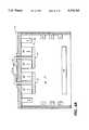
- FIG. 1is an axially sectioned generally schematic representation of a plasma forming chamber constructed in accordance with the present invention and particularly adapted for use in chemical vapor deposition or etching of specimens such as VLSI wafers, sectioning lines being omitted for clarity.
- FIG. 2illustrates an alternate embodiment of the invention including a fused quartz chamber.
- FIG. 3illustrates a separate embodiment including an all-metal chamber.
- FIG. 4Ais a sectioned view in elevation illustrating a large rectilinear array applicator.
- FIG. 4Bis a fragmentary plan view of the rectilinear array applicator.
- FIG. 5is a similar view of another embodiment of the plasma forming apparatus of the present invention adapted for use in other applications such as a negative ion source.
- FIG. 6is a fragmentary representation of a novel applicator and coupler for the invention, the applicator being formed as paired elements.
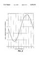
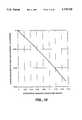
- FIG. 7is a graphical representation illustrating the effects of arbitrary values of the initial gyrophase angle.
- FIG. 8illustrates a numerical evaluation of the gyrophase average from FIG. 7.
- FIG. 9illustrates the gyro-period averaged displacement as a function of the initial gyrophase angle.
- FIG. 10illustrates the average over initial gyrophase for a range of values of ⁇ 0 /L.
- a novel electron cyclotron resonance plasma source constructed according to the present inventionis indicated at 10 and is contemplated for producing or generating a large diameter or cross-sectional stream of uniform, low-temperature plasma, even when low background gas pressures are maintained in the plasma source or chamber.
- the plasma source 10comprises a chamber or enclosure 12 which is preferably a cylinder symmetrical about its longitudinal axis 14 for purposes described in greater detail below.
- Neutral reactant gas mixturesare introduced into the chamber 12 in a generally conventional manner from a source 16.
- the chamber 12is also provided with high-speed vacuum pumps schematically indicated at 18 and adapted for maintaining low background gas pressure within the chamber in a preferred operating range of about 10 -5 -10 -4 Torr.
- the purpose for the preferred low pressure background gasis also discussed in greater detail below.
- FIG. 2An alternative embodiment that employs a fused quartz chamber is shown in FIG. 2.
- FIG. 3A separate embodiment especially suited for use in an all-metal chamber is shown in FIG. 3.
- FIG. 4A large rectilinear array applicator is shown in FIG. 4.
- the generic source shown in FIG. 1is first described below.
- symmetric magnetic field force linesare formed within the chamber 12 by a plurality of cylindrical arrays of permanent magnets generally indicated at 20.
- two ring-shaped cylindrical magnet assemblies 22 and 24are arranged about the circumference of a plasma forming portion 26 for developing magnetic field force lines which are configured as cylindrical lobes.
- lobed magnetic field force linesare indicated at 28, 30 and 32 for the cylindrical magnetic assembly 22.
- lobed magnetic field force lines 34, 36 and 38are illustrated for the other cylindrical magnetic assembly 24.
- magnet assemblies 22 and 24are cylindrical and generally symmetrical about the circumference of the chamber 12 so that each adjacent pair of lobed magnetic field force lines, principally those indicated at 28, 30 and 34, 36 form annular magnetic mirror regions indicated respectively at 40 and 42. Those regions are shown with cross hatching in order to better emphasize the locations of the magnetic mirror regions 40 and 42.
- a microwave power source 44is arranged between the magnet arrays 22 and 24 adjacent the plasma forming portion 26 of the chamber.
- the microwave power source 44is provided with one or more pairs of annular sectors of slotted wave guide microwave applicators 46 through which the microwave power is introduced into the plasma forming portion 26 of the chamber.
- the microwave poweris introduced along multiple injection axes indicated by the arrows 48 which extend perpendicular to the chamber axis 14.
- the slotted wave guide microwave applicators 46novelly causes the microwave power to be uniformly introduced about the entire periphery of the chamber.
- the injection axes 48are all radially arranged relative to the longitudinal axis 14.
- the magnetic intensitydecreases from a local maximum at the location of the slotted wave guide to the resonant value so as to permit over-dense operation as described above.
- each elementis a slotted-waveguide antenna formed in the shape of an arc so that the complete applicator comprises a full circle that circumferentially encloses the plasma.
- a hybrid coupler 47which provides a stable match to the variable impedance of the plasma without the necessity of the usual tuning stubs (not shown). It also reduces the microwave power density passing through each of the windows required for introducing microwave power into the highly evacuated interior of the microwave source.
- the hybrid coupleris well known to those skilled in the art and is novel within the invention only in combination with the paired applicators.
- the first requirement for magnetic-field configurationis that it must permit microwave illumination of the resonant interaction region with the applicator positioned for high-field launch of plasma waves. If the radiating surface of the applicator is at a radial position given by r applicator , and the resonant interaction region is at a radial position given by r resonance , it is required that the magnetic field strength satisfy the equation
- f.sub. ⁇is the frequency of the microwave power
- m and eare the mass and electric charge of the electron
- cis the speed of light in vacuum. Additionally, the magnetic field strength in the evacuated portions of the waveguide must exceed B resonance in order to prevent RF breakdown.
- the magnetic field lines adjacent to the applicatorhave the additional function of confining energetic electrons in magnetic-mirror traps. This magnetic-mirror confinement inhibits the spatial transport of the energetic electrons to minimize the plasma-wall interaction and thereby reduce the rate of wall erosion and impurity generation, while increasing the efficiency with which gas is ionized to form the useful plasma. Specifically, it is required that these magnetic lines of force have the (axisymmetric) lobe-shaped configuration as illustrated. Regions where the field lines converge are regions of high magnetic field strength; i.e., magnetic mirrors.
- the lobe-shaped magnetic field linesprevent some of the electrons from moving directly from the resonant interaction region to the sample being processed. Instead, the geometrical configuration of the magnetic field causes plasma to flow radially inward into the region of low magnetic field strength.
- an outlet 50is formed at one axial end of the chamber 12.
- the other axial end of the chamber 12is closed by a wall 52 and an additional permanent magnet array 54 which assists in developing the magnetic field within the plasma forming portion 26 of the chamber with the desired central field-free region.
- the magnet array 54conventionally forms magnetic insulation for the end wall 52.
- a similar insulating functionis also performed by the cylindrical magnet array 20 and particularly the cylindrical magnet assemblies 22 and 24.
- the microwave power source 44With the microwave power source 44 arranged as described, it is important to note that energetic electrons formed by interaction of the microwave power with background plasma existing in the chamber are prevented from direct line-of-sight communication with the specimens 56. Rather, the energetic electrons formed by the microwave power may be considered in two classes first.
- a first class of the energetic electronstend to enter the central region of the plasma forming chamber portion 26 where they impinge or collide with field force lines such as those indicated at 28-30 as they are transported radially into the central field-free region. Energetic electrons in this first class thus tend to bounce back and forth laterally within the plasma forming chamber portion 26 until they eventually interact or collide with neutral gas atoms and degrade in energy to assist in increasing density of the cold plasma.
- the second class of energetic electronsis dependent upon the arrangement of the microwave power source 44 adjacent and preferably intermediate the two cylindrical magnet assemblies 22 and 24. This second class of energetic electrons is captured within magnetic mirror regions such as those indicated at 40 and 42.
- the symmetrical configuration of the cylindrical chamber 12 together with the interacting arrangement of the cylindrical magnet assemblies 22, 24 and the microwave power source 44produces great efficiency in converting the microwave power into cold plasma while also preventing line-of-sight communication of the energetic electrons with the specimens 56 as noted above.
- a wafer 56is arranged upon a holder 58 in communication with the outlet 50.
- a magnetic field free region 60is formed in the chamber 12 intermediate the plasma forming chamber portion 26 and the outlet 50.
- Insulating magnets 62are also arranged about the circumference of the magnetic field free region 60 in order to prevent plasma in the region 60 from colliding with adjacent wall portions of the chamber as well as to reduce the interior magnetic field strength to sufficiently low values.
- the microwave power source 44 and the magnetsare adapted for producing a resonant interaction region generally indicated as a continuous surface at 64.
- the resonant heating region 64extends substantially into the plasma producing chamber portion 26 while being absent from the magnetic field free region. It is of course to be understood that energy in energetic electrons passing through the resonant region 64 is increased.
- the first class of energetic electrons referred to abovetends to pass through the region 64 only once and thereafter to remain in a central portion of the plasma forming chamber 26 until interacting with gas atoms as described above.
- the second class of energetic electrons which precess in the magnetic mirror regions have their energy levelsfurther increases since they are capable of passing through the resonant region 64 numerous times while precessing about the circumference of the chamber. For that reason, the magnets are designed so that the resonant heating envelope 64 preferably intersects the magnetic mirror regions 40 and 42 in order to achieve elevated energy levels for the energetic electrons therein.
- impurity trapping recesses 66 and 68are annularly formed adjacent the cylindrical magnet assemblies 22 and 24. Thus, any energetic electrons and accompanying ions tending to leak out of the magnetic mirror regions 40 and 42 enter into the recesses 66 and 68.
- energetic electrons in the recess 66are prevented from line-of-sight communication with the outlet 50 by means of an annular deflector 70 generally arranged between the recess 66 and the magnetic field free region 60.
- Wall surfaces in the recesses 66 and 68are preferably formed from a suitable dielectric material in order to minimize sputtering of wall material.
- the inventionalso contemplates providing means either in or in communication with the recesses 66 and 68 to further prevent the energetic electrons or impurities within the recesses 66 and 68 from entering the plasma forming chamber portion 26.
- cryogenic surfaces 72may be formed in the recesses for trapping the energetic electrons and impurities for that region.
- high vacuum sources(not shown) could be arranged in communication with the recesses 66 and 68 for the same purpose.
- each of the cylindrical magnet assemblies 22 and 24is formed with a principle cylindrical magnet 74 or 76 generally facing the plasma forming chamber portion 26. Additional paired magnets 78, 80 and 82, 84 are arranged behind the principle magnets with their polar axes diagonally oriented as illustrated by the arrows so that the magnetic field force lines are closely drawn about the magnet assemblies as illustrated in FIG. 1.
- Alternative combinations of magnetic materialscan be devised to yield magnetic configurations that satisfy all the requirements identified herein. The particular choice shown in FIG. 1 illustrates only one of several practical embodiments. Others are illustrated below.
- the cylindrical magnet assemblies 22 and 24also prevent the magnetic field force lines from extending into the magnetic field free region 60 so that it is better able to accomplish its function.
- energetic electronsare initially formed by interaction of microwave power from the source 44 with background plasma initially present in the plasma forming portion 26 of the chamber.
- Two classes of energetic electronsare formed as described above, both of which are prevented from direct line-of-sight communication with the outlet 50.
- the magnets and the microwave power sourceBecause of the design of the cylindrical chamber 12, the magnets and the microwave power source, high efficiency is accomplished in conversion of energetic electrons to increase the density of the cold plasma. Furthermore, with low pressure being maintained in the chamber, the plasma flow to the substrate is also unidirectional or anisotropic as also discussed above. As cold plasma flows or streams from the plasma forming chamber portion 26 toward the outlet 50, it passes into the magnetic field free region 60. In that region, because of the substantial absence of magnetic field force lines, the cold plasma expands freely in the transverse direction and becomes very uniform in density as it approaches the outlet 50. Thus, as plasma streams through the magnetic field free region 60 toward the outlet 50, it is characterized not only by high current density but also by uniformity of plasma density in order to greatly enhance the uniformity of chemical vapor deposition or etching on the specimen 56.
- the plasma source of the present inventionmay also be used as a negative ion source with substantially all components of the plasma source being similar to those described herein.
- Other related applicationsare also of course possible for the method and apparatus of the invention.
- FIG. 2indicates schematically how the microwave applicator 46' can be used in conjunction with a fused quartz liner 49.
- the applicator 46'can be operated at atmospheric pressure, since fused quartz is an entirely satisfactory material for forming a microwave window needed to separate the partially evacuated plasma region from atmospheric pressure. For the microwave power levels of interest here, breakdown will not occur inside the applicator if it is operated at atmospheric pressure, regardless of the value of the magnetic field strength within the applicator. Thus, the requirements that the magnetic field configuration must satisfy can be substantially relaxed.
- the trough between the main rings of permanent magnets in which the applicator 46' is locatedcan be open around the entire circumference.
- the magnetic configurationcan thereby approximate more nearly the desired axisymmetry; since the symmetry need not be broken by localized penetrations to accommodate the microwave power coupling structures.
- This enhanced degree of azimuthal uniformityis expected to substantially increase the plasma uniformity by avoiding residual non-axisymmetric magnetic field structures that tend to impress a corresponding structure on the plasma itself.
- the magnetic fieldis very efficiently generated by using rings of permanent magnets oriented generally as shown in FIG. 2, in conjunction with rings of mild steel that are indicated there. Structures of the general type shown in the figure meet the several requirements that have been specified earlier.
- mild-steel bands 51are movably inserted at the position of the permanent magnet pole faces to permit final adjustments to the magnetic field configuration after the permanent magnets have been installed, thereby relaxing what would otherwise be excessively stringent magnetic fabrication tolerances.
- These mild-steel bandsare particularly beneficial in that they can be moved small distances along the axis of the cylindrical array to adjust the value of the magnetic field strength on the axis of the chamber to the exact value required to allow the plasma to expand more freely in the radial direction, i.e., in the direction transverse to the axis of the chamber.
- FIG. 3indicates schematically how the applicator 46" is adapted to form plasmas in an all-metallic chamber.
- the evacuated portion of the applicatoris isolated from atmospheric pressure by a suitable internal microwave window (not shown).
- B resThe magnetic intensity everywhere inside the evacuated portion of the applicator must exceed the resonance value, B res , in order to prevent microwave breakdown inside the applicator.
- B res2 ⁇ (m/e)f.sub. ⁇ , where these symbols have been defined previously.
- the applicator formed from narrow-height waveguidebeing slotted on its broad face, it can be located directly in front of the pole face of a ring of permanent magnets, as shown in FIG. 3. In this way, it is possible to meet the requirements for prevention of breakdown in a particularly efficient way and thereby minimize the weight and cost of the permanent magnet system.
- the microwave windowis placed at the end of the applicator adjacent to the waveguide coupler that connects the applicator to the microwave power generator, so that all of the evacuated portions of the applicator are in a magnetic field that exceeds the electron cyclotron resonance value.
- the narrow-height waveguide couplercan be brought out in the axial direction without penetrating any of the permanent magnet rings, thereby preserving the symmetry of the magnetic field.
- FIGS. 4A and 4Billustrate how the microwave applicator or applicators 101 are adapted for use in a large-area rectilinear array 102 for treating specimens 103 with very large surface areas.
- the figuresdisplay a cross-section through rows 104 of permanent magnets 105 magnetized in the directions shown by arrows and mounted on a mild steel shell 106.
- the applicatorsare formed from straight sections of waveguide slotted on the broad face, as was also the case in the all-metal system.
- the embodiment shown schematically in FIGS. 4A and 4Bis suitable for treating large, flat specimens; but the rectilinear array of slotted-waveguide applicators can readily be shaped in cross-section to conform to large curved surfaces. Such a conformal array of applicators could be used to ensure uniform treatment of very large curved surfaces.
- the sample to be treatedis directly opposite the resonant interaction region, and will thus be accessible to energetic electrons generated by the electron cyclotron heating process.
- the generation of bursts of energetic electronsis ameliorated by the distribution of the heating power over a large area, it is intended that this approach be utilized for applications that are not highly sensitive to damage, such as deposition of diamond films, ion implantation or other types of surface modification, etc.
- the first referenceis a paper by B. H. Quon and R. A. Dandl entitled "Preferential electron-cyclotron heating of hot electrons and formation of overdense plasmas", Phys. Fluids B 1 (10), October 1989.
- the second referenceis a paper by G. E. Guest, M. E. Fetzer and R. A. Dandl entitled "Whistler-wave electron cyclotron heating in uniform and nonuniform magnetic fields", Phys. Fluids B 2 (6), June 1990.
- the third referenceis a paper by R. A. Dandl and G. E. Guest entitled “On the low-pressure mode transition in electron cyclotron heated plasmas", J. Vac. Sci. Technol. A 9 (6), November/December 1991.
- the first paperrelates to experimental work leading to the theoretical interpretation of the present invention.
- the experimental work described in that papersupports the disclosed embodiments of the invention.
- the second and third referencesrelate to theoretical interpretation of the invention as developed following the experimental work set forth in the first paper.
- Magnetic bucketsmay need to include the present mechanism to account for plasma flow into the central region of very low magnetic field strength.
- v.sub. ⁇is the component of the particle's velocity perpendicular to B
- L -1B -1 dB/dy
- m and qare the mass and charge of the particle, respectively.
- the particle orbitsare displaced in the direction opposite to the magnetic field gradient, as can readily be seen from the following heuristic argument.
- FIG. 9shows the gyro-period averaged displacement as a function of the initial gyrophase angle; and FIG. 10 shows the average over initial gyrophase for a range of values of ⁇ 0 /L. From this data we find
- n eis the density of the stream of precessing electrons
- pis their pressure, assumed isotropic.
Landscapes
- Physics & Mathematics (AREA)
- Engineering & Computer Science (AREA)
- Plasma & Fusion (AREA)
- Chemical & Material Sciences (AREA)
- Analytical Chemistry (AREA)
- Optics & Photonics (AREA)
- Spectroscopy & Molecular Physics (AREA)
Abstract
Description
B(r.sub.resonance)=2πf.sub.μ m/e=B.sub.resonance
B(r.sub.applicator)>1.5 B.sub.resonance
r.sub.applicator -r.sub.resonance ˜c/f.sub.μ,
v.sub.g =(mv.sub.⊥.sup.2 /2q)[(Bx∇B)/B.sup.3 ]=-mv.sub.⊥.sup.2 /(2qBL)e.sub.x.
y(t)=y.sub.bd +ρ.sub.1 sin (Ω.sub.1 t), 0≦t≦π/Ω.sub.1, where
ρ.sub.1 =v.sub.⊥ /Ω.sub.1 and Ω.sub.1 =eB.sub.1 /m.sub.e.
<y-y.sub.bd >=2(ρ.sub.1 -ρ.sub.2)/π=(2m.sub.e /πe)v.sub.⊥ (B.sub.1.sup.-1 -B.sub.2.sup.-1).
B(y)=B.sub.0 [1+(y-y.sub.0)/L]e.sub.z
<<(y-y.sub.0)/ρ.sub.0 >>=-ρ.sub.0 /3L;
<<(y-y.sub.0)>>=-ρ.sub.0.sup.2 /3L.
<<dy/dt>>=-ρ.sub.0.sup.2 υ.sub.φ /3L.
n.sub.e m.sub.e (dv/dt)=-∇p-en.sub.e E+jxB+F.sub.vis.
F.sub.vis =-v.sub.vis n.sub.e m.sub.e v.sub.x e.sub.x.
0=-∇p-en.sub.e E+jxB-υ.sub.vis n.sub.e m.sub.e v.sub.x e.sub.x.
0=-Bx∇p-en.sub.e BxE+Bx(jxB)-υ.sub.vis n.sub.e m.sub.e BV.sub.x e.sub.y.
j.sub.y =υ.sub.vis n.sub.e m.sub.e v.sub.x /B=υ.sub.vis n.sub.e m.sub.e.sup.2 v.sub.⊥.sup.2 /(2eB.sup.2 L)=-en.sub.e <v.sub.y >.
<v.sub.y >=-υ.sub.vis ρ.sup.2 /2L.
Claims (17)
Priority Applications (1)
| Application Number | Priority Date | Filing Date | Title |
|---|---|---|---|
| US08/048,744US5370765A (en) | 1989-03-09 | 1993-04-16 | Electron cyclotron resonance plasma source and method of operation |
Applications Claiming Priority (3)
| Application Number | Priority Date | Filing Date | Title |
|---|---|---|---|
| US07/320,947US5133826A (en) | 1989-03-09 | 1989-03-09 | Electron cyclotron resonance plasma source |
| US07/875,750US5203960A (en) | 1989-03-09 | 1992-04-29 | Method of operation of electron cyclotron resonance plasma source |
| US08/048,744US5370765A (en) | 1989-03-09 | 1993-04-16 | Electron cyclotron resonance plasma source and method of operation |
Related Parent Applications (1)
| Application Number | Title | Priority Date | Filing Date |
|---|---|---|---|
| US07/875,750Continuation-In-PartUS5203960A (en) | 1989-03-09 | 1992-04-29 | Method of operation of electron cyclotron resonance plasma source |
Publications (1)
| Publication Number | Publication Date |
|---|---|
| US5370765Atrue US5370765A (en) | 1994-12-06 |
Family
ID=46247285
Family Applications (1)
| Application Number | Title | Priority Date | Filing Date |
|---|---|---|---|
| US08/048,744Expired - LifetimeUS5370765A (en) | 1989-03-09 | 1993-04-16 | Electron cyclotron resonance plasma source and method of operation |
Country Status (1)
| Country | Link |
|---|---|
| US (1) | US5370765A (en) |
Cited By (67)
| Publication number | Priority date | Publication date | Assignee | Title |
|---|---|---|---|---|
| US5536914A (en)* | 1993-02-25 | 1996-07-16 | Metal Process (Societe A Responsabilite Limitee) | Device for exciting a plasma to electron cyclotron resonance by means of a wire applicator of a static magnetic field and of a microwave field |
| US5537004A (en)* | 1993-03-06 | 1996-07-16 | Tokyo Electron Limited | Low frequency electron cyclotron resonance plasma processor |
| US5538699A (en)* | 1991-11-05 | 1996-07-23 | Canon Kabushiki Kaisha | Microwave introducing device provided with an endless circular waveguide and plasma treating apparatus provided with said device |
| US5567268A (en)* | 1994-01-31 | 1996-10-22 | Sony Corporation | Plasma processing apparatus and method for carrying out plasma processing by using such plasma processing apparatus |
| US5653811A (en)* | 1995-07-19 | 1997-08-05 | Chan; Chung | System for the plasma treatment of large area substrates |
| EP0764969A3 (en)* | 1995-09-21 | 1997-11-12 | Canon Kabushiki Kaisha | Microwave plasma processing apparatus and microwave plasma processing method |
| US5707452A (en)* | 1996-07-08 | 1998-01-13 | Applied Microwave Plasma Concepts, Inc. | Coaxial microwave applicator for an electron cyclotron resonance plasma source |
| WO1999012184A3 (en)* | 1997-09-05 | 1999-05-27 | Alcad Pro Inc | Microwave power applicator for generating reactive chemical species from gaseous reagent species |
| WO1999035302A1 (en)* | 1998-01-12 | 1999-07-15 | Applied Microwave Plasma Concepts, Inc. | Coaxial resonant multiport microwave applicator for an ecr plasma source |
| US5961773A (en)* | 1996-03-28 | 1999-10-05 | Hitachi, Ltd. | Plasma processing apparatus and plasma processing method using the same |
| US5975855A (en)* | 1996-12-03 | 1999-11-02 | Microwave Plasma Products, Inc. | Method and apparatus for increasing channel plasma density in an MHD vacuum pump |
| US5981955A (en)* | 1995-12-07 | 1999-11-09 | The Regents Of The University Of California | Isotope separation using a high field source and improved collectors |
| US5985742A (en)* | 1997-05-12 | 1999-11-16 | Silicon Genesis Corporation | Controlled cleavage process and device for patterned films |
| US6007878A (en)* | 1993-05-27 | 1999-12-28 | Canon Kabushiki Kaisha | Process for producing an optical recording medium having a protective layer formed using a plasma processing device |
| US6027988A (en)* | 1997-05-28 | 2000-02-22 | The Regents Of The University Of California | Method of separating films from bulk substrates by plasma immersion ion implantation |
| US6051073A (en)* | 1998-02-11 | 2000-04-18 | Silicon Genesis Corporation | Perforated shield for plasma immersion ion implantation |
| US6103599A (en)* | 1997-07-25 | 2000-08-15 | Silicon Genesis Corporation | Planarizing technique for multilayered substrates |
| WO2000037206A3 (en)* | 1998-12-23 | 2000-11-02 | Applied Science & Tech Inc | Permanent magnet ecr plasma source with integrated multipolar magnetic confinement |
| US6213050B1 (en) | 1998-12-01 | 2001-04-10 | Silicon Genesis Corporation | Enhanced plasma mode and computer system for plasma immersion ion implantation |
| US6221740B1 (en) | 1999-08-10 | 2001-04-24 | Silicon Genesis Corporation | Substrate cleaving tool and method |
| US6228176B1 (en) | 1998-02-11 | 2001-05-08 | Silicon Genesis Corporation | Contoured platen design for plasma immerson ion implantation |
| US6263941B1 (en) | 1999-08-10 | 2001-07-24 | Silicon Genesis Corporation | Nozzle for cleaving substrates |
| US20010011525A1 (en)* | 2000-02-07 | 2001-08-09 | Yasuyoshi Yasaka | Microwave plasma processing system |
| US6284631B1 (en) | 1997-05-12 | 2001-09-04 | Silicon Genesis Corporation | Method and device for controlled cleaving process |
| US6291326B1 (en) | 1998-06-23 | 2001-09-18 | Silicon Genesis Corporation | Pre-semiconductor process implant and post-process film separation |
| US6291313B1 (en) | 1997-05-12 | 2001-09-18 | Silicon Genesis Corporation | Method and device for controlled cleaving process |
| US6390019B1 (en)* | 1998-06-11 | 2002-05-21 | Applied Materials, Inc. | Chamber having improved process monitoring window |
| EP1113522A3 (en)* | 1999-12-29 | 2002-05-29 | Lg Electronics Inc. | Coupling structure of waveguide and applicator, and its application to electrodeless lamp |
| US6458723B1 (en) | 1999-06-24 | 2002-10-01 | Silicon Genesis Corporation | High temperature implant apparatus |
| US6500732B1 (en) | 1999-08-10 | 2002-12-31 | Silicon Genesis Corporation | Cleaving process to fabricate multilayered substrates using low implantation doses |
| US6514838B2 (en) | 1998-02-17 | 2003-02-04 | Silicon Genesis Corporation | Method for non mass selected ion implant profile control |
| US6541781B1 (en) | 2000-07-25 | 2003-04-01 | Axcelis Technologies, Inc. | Waveguide for microwave excitation of plasma in an ion beam guide |
| US6548382B1 (en) | 1997-07-18 | 2003-04-15 | Silicon Genesis Corporation | Gettering technique for wafers made using a controlled cleaving process |
| US20030122492A1 (en)* | 2000-04-13 | 2003-07-03 | Dandl Raphael A. | Stand alone plasma vacuum pump |
| US6607633B2 (en) | 2000-01-20 | 2003-08-19 | Y.A.C. Co, Ltd. | Plasma generating device and plasma processing apparatus comprising such a device |
| US6673199B1 (en) | 2001-03-07 | 2004-01-06 | Applied Materials, Inc. | Shaping a plasma with a magnetic field to control etch rate uniformity |
| US20040076837A1 (en)* | 2002-10-22 | 2004-04-22 | Schlage Lock Co. | Corrosion-resistant coatings and methods of manufacturing the same |
| US6729850B2 (en) | 2001-10-31 | 2004-05-04 | Tokyo Electron Limited | Applied plasma duct system |
| US6787200B1 (en)* | 1999-07-01 | 2004-09-07 | Commissariat A L'energie Atomique | Method and device for electronic cyclotronic resonance plasma deposit of carbon nanofibre layers in fabric form and resulting fabric layers |
| US20040226511A1 (en)* | 2001-04-20 | 2004-11-18 | Applied Materials, Inc. | Multi-core transformer plasma source |
| US20040227106A1 (en)* | 2003-05-13 | 2004-11-18 | Halling Alfred M. | System and methods for ion beam containment using localized electrostatic fields in an ion beam passageway |
| US6831742B1 (en) | 2000-10-23 | 2004-12-14 | Applied Materials, Inc | Monitoring substrate processing using reflected radiation |
| US20060011583A1 (en)* | 1999-11-15 | 2006-01-19 | Bailey Andrew D Iii | Materials and gas chemistries for processing systems |
| US7056808B2 (en) | 1999-08-10 | 2006-06-06 | Silicon Genesis Corporation | Cleaving process to fabricate multilayered substrates using low implantation doses |
| US7067034B2 (en)* | 2000-03-27 | 2006-06-27 | Lam Research Corporation | Method and apparatus for plasma forming inner magnetic bucket to control a volume of a plasma |
| US20090034657A1 (en)* | 2007-08-03 | 2009-02-05 | Nikolova Natalia K | Electromagnetic wave-potential communication system |
| US7493869B1 (en) | 2005-12-16 | 2009-02-24 | The United States Of America As Represented By The Administration Of Nasa | Very large area/volume microwave ECR plasma and ion source |
| US20100109532A1 (en)* | 2006-07-12 | 2010-05-06 | Jacques Pelletier | Device and method for producing and/or confining a plasma |
| US7776717B2 (en) | 1997-05-12 | 2010-08-17 | Silicon Genesis Corporation | Controlled process and resulting device |
| US7811900B2 (en) | 2006-09-08 | 2010-10-12 | Silicon Genesis Corporation | Method and structure for fabricating solar cells using a thick layer transfer process |
| US20110215722A1 (en)* | 2008-10-30 | 2011-09-08 | Centre National De La Recherche Scientifique (Cnrs ) | Device and method for producing and/or confining a plasma |
| US8187377B2 (en) | 2002-10-04 | 2012-05-29 | Silicon Genesis Corporation | Non-contact etch annealing of strained layers |
| US8293619B2 (en) | 2008-08-28 | 2012-10-23 | Silicon Genesis Corporation | Layer transfer of films utilizing controlled propagation |
| US8329557B2 (en) | 2009-05-13 | 2012-12-11 | Silicon Genesis Corporation | Techniques for forming thin films by implantation with reduced channeling |
| US8330126B2 (en) | 2008-08-25 | 2012-12-11 | Silicon Genesis Corporation | Race track configuration and method for wafering silicon solar substrates |
| US8993410B2 (en) | 2006-09-08 | 2015-03-31 | Silicon Genesis Corporation | Substrate cleaving under controlled stress conditions |
| US9048518B2 (en) | 2011-06-21 | 2015-06-02 | Applied Materials, Inc. | Transmission line RF applicator for plasma chamber |
| US9362439B2 (en) | 2008-05-07 | 2016-06-07 | Silicon Genesis Corporation | Layer transfer of films utilizing controlled shear region |
| US9397380B2 (en) | 2011-01-28 | 2016-07-19 | Applied Materials, Inc. | Guided wave applicator with non-gaseous dielectric for plasma chamber |
| US20210082670A1 (en)* | 2019-09-16 | 2021-03-18 | The Regents Of The University Of Michigan | Multiple frequency electron cyclotron resonance thruster |
| US11037765B2 (en)* | 2018-07-03 | 2021-06-15 | Tokyo Electron Limited | Resonant structure for electron cyclotron resonant (ECR) plasma ionization |
| US20240071725A1 (en)* | 2022-08-25 | 2024-02-29 | 6K Inc. | Plasma apparatus and methods for processing feed material utiziling a powder ingress preventor (pip) |
| US12176529B2 (en) | 2020-06-25 | 2024-12-24 | 6K Inc. | Microcomposite alloy structure |
| US12195338B2 (en) | 2022-12-15 | 2025-01-14 | 6K Inc. | Systems, methods, and device for pyrolysis of methane in a microwave plasma for hydrogen and structured carbon powder production |
| US12261023B2 (en) | 2022-05-23 | 2025-03-25 | 6K Inc. | Microwave plasma apparatus and methods for processing materials using an interior liner |
| US12279357B1 (en)* | 2023-11-03 | 2025-04-15 | W. Davis Lee | Electron resonance source apparatus and method of use thereof |
| US12406829B2 (en) | 2021-01-11 | 2025-09-02 | 6K Inc. | Methods and systems for reclamation of Li-ion cathode materials using microwave plasma processing |
Citations (3)
| Publication number | Priority date | Publication date | Assignee | Title |
|---|---|---|---|---|
| US4745337A (en)* | 1985-06-07 | 1988-05-17 | Centre National D'etudes Des Telecommunications | Method and device for exciting a plasma using microwaves at the electronic cyclotronic resonance |
| US4776918A (en)* | 1986-10-20 | 1988-10-11 | Hitachi, Ltd. | Plasma processing apparatus |
| US5133826A (en)* | 1989-03-09 | 1992-07-28 | Applied Microwave Plasma Concepts, Inc. | Electron cyclotron resonance plasma source |
- 1993
- 1993-04-16USUS08/048,744patent/US5370765A/ennot_activeExpired - Lifetime
Patent Citations (3)
| Publication number | Priority date | Publication date | Assignee | Title |
|---|---|---|---|---|
| US4745337A (en)* | 1985-06-07 | 1988-05-17 | Centre National D'etudes Des Telecommunications | Method and device for exciting a plasma using microwaves at the electronic cyclotronic resonance |
| US4776918A (en)* | 1986-10-20 | 1988-10-11 | Hitachi, Ltd. | Plasma processing apparatus |
| US5133826A (en)* | 1989-03-09 | 1992-07-28 | Applied Microwave Plasma Concepts, Inc. | Electron cyclotron resonance plasma source |
Cited By (118)
| Publication number | Priority date | Publication date | Assignee | Title |
|---|---|---|---|---|
| US5538699A (en)* | 1991-11-05 | 1996-07-23 | Canon Kabushiki Kaisha | Microwave introducing device provided with an endless circular waveguide and plasma treating apparatus provided with said device |
| US5536914A (en)* | 1993-02-25 | 1996-07-16 | Metal Process (Societe A Responsabilite Limitee) | Device for exciting a plasma to electron cyclotron resonance by means of a wire applicator of a static magnetic field and of a microwave field |
| US5537004A (en)* | 1993-03-06 | 1996-07-16 | Tokyo Electron Limited | Low frequency electron cyclotron resonance plasma processor |
| US6007878A (en)* | 1993-05-27 | 1999-12-28 | Canon Kabushiki Kaisha | Process for producing an optical recording medium having a protective layer formed using a plasma processing device |
| US5567268A (en)* | 1994-01-31 | 1996-10-22 | Sony Corporation | Plasma processing apparatus and method for carrying out plasma processing by using such plasma processing apparatus |
| US5653811A (en)* | 1995-07-19 | 1997-08-05 | Chan; Chung | System for the plasma treatment of large area substrates |
| US6338313B1 (en) | 1995-07-19 | 2002-01-15 | Silison Genesis Corporation | System for the plasma treatment of large area substrates |
| US6632324B2 (en) | 1995-07-19 | 2003-10-14 | Silicon Genesis Corporation | System for the plasma treatment of large area substrates |
| EP0764969A3 (en)* | 1995-09-21 | 1997-11-12 | Canon Kabushiki Kaisha | Microwave plasma processing apparatus and microwave plasma processing method |
| US5985091A (en)* | 1995-09-21 | 1999-11-16 | Canon Kabushiki Kaisha | Microwave plasma processing apparatus and microwave plasma processing method |
| US5981955A (en)* | 1995-12-07 | 1999-11-09 | The Regents Of The University Of California | Isotope separation using a high field source and improved collectors |
| US5961773A (en)* | 1996-03-28 | 1999-10-05 | Hitachi, Ltd. | Plasma processing apparatus and plasma processing method using the same |
| US6332947B1 (en) | 1996-03-28 | 2001-12-25 | Hitachi, Ltd. | Plasma processing apparatus and plasma processing method using the same |
| US5707452A (en)* | 1996-07-08 | 1998-01-13 | Applied Microwave Plasma Concepts, Inc. | Coaxial microwave applicator for an electron cyclotron resonance plasma source |
| WO1998001599A1 (en) | 1996-07-08 | 1998-01-15 | Applied Microwave Plasma Concepts, Inc. | Microwave applicator for an electron cyclotron resonance plasma source |
| US5975014A (en)* | 1996-07-08 | 1999-11-02 | Asm Japan K.K. | Coaxial resonant multi-port microwave applicator for an ECR plasma source |
| JP2000514595A (en)* | 1996-07-08 | 2000-10-31 | アプライド、マイクロウェーブ、プラズマ、コンセプツ、インコーポレーテッド | Coaxial microwave applicator for electron cyclotron resonant plasma source |
| US5975855A (en)* | 1996-12-03 | 1999-11-02 | Microwave Plasma Products, Inc. | Method and apparatus for increasing channel plasma density in an MHD vacuum pump |
| US7410887B2 (en) | 1997-05-12 | 2008-08-12 | Silicon Genesis Corporation | Controlled process and resulting device |
| US7160790B2 (en) | 1997-05-12 | 2007-01-09 | Silicon Genesis Corporation | Controlled cleaving process |
| US6486041B2 (en) | 1997-05-12 | 2002-11-26 | Silicon Genesis Corporation | Method and device for controlled cleaving process |
| US6048411A (en)* | 1997-05-12 | 2000-04-11 | Silicon Genesis Corporation | Silicon-on-silicon hybrid wafer assembly |
| US7759217B2 (en) | 1997-05-12 | 2010-07-20 | Silicon Genesis Corporation | Controlled process and resulting device |
| US6458672B1 (en) | 1997-05-12 | 2002-10-01 | Silicon Genesis Corporation | Controlled cleavage process and resulting device using beta annealing |
| US6010579A (en)* | 1997-05-12 | 2000-01-04 | Silicon Genesis Corporation | Reusable substrate for thin film separation |
| US7371660B2 (en) | 1997-05-12 | 2008-05-13 | Silicon Genesis Corporation | Controlled cleaving process |
| US6146979A (en)* | 1997-05-12 | 2000-11-14 | Silicon Genesis Corporation | Pressurized microbubble thin film separation process using a reusable substrate |
| US6155909A (en)* | 1997-05-12 | 2000-12-05 | Silicon Genesis Corporation | Controlled cleavage system using pressurized fluid |
| US6159825A (en)* | 1997-05-12 | 2000-12-12 | Silicon Genesis Corporation | Controlled cleavage thin film separation process using a reusable substrate |
| US6159824A (en)* | 1997-05-12 | 2000-12-12 | Silicon Genesis Corporation | Silicon-on-silicon wafer bonding process using a thin film blister-separation method |
| US6162705A (en)* | 1997-05-12 | 2000-12-19 | Silicon Genesis Corporation | Controlled cleavage process and resulting device using beta annealing |
| US6187110B1 (en) | 1997-05-12 | 2001-02-13 | Silicon Genesis Corporation | Device for patterned films |
| US7348258B2 (en) | 1997-05-12 | 2008-03-25 | Silicon Genesis Corporation | Method and device for controlled cleaving process |
| US6013563A (en)* | 1997-05-12 | 2000-01-11 | Silicon Genesis Corporation | Controlled cleaning process |
| US6790747B2 (en) | 1997-05-12 | 2004-09-14 | Silicon Genesis Corporation | Method and device for controlled cleaving process |
| US6245161B1 (en) | 1997-05-12 | 2001-06-12 | Silicon Genesis Corporation | Economical silicon-on-silicon hybrid wafer assembly |
| US6632724B2 (en) | 1997-05-12 | 2003-10-14 | Silicon Genesis Corporation | Controlled cleaving process |
| US5994207A (en)* | 1997-05-12 | 1999-11-30 | Silicon Genesis Corporation | Controlled cleavage process using pressurized fluid |
| US6284631B1 (en) | 1997-05-12 | 2001-09-04 | Silicon Genesis Corporation | Method and device for controlled cleaving process |
| US6558802B1 (en) | 1997-05-12 | 2003-05-06 | Silicon Genesis Corporation | Silicon-on-silicon hybrid wafer assembly |
| US6291313B1 (en) | 1997-05-12 | 2001-09-18 | Silicon Genesis Corporation | Method and device for controlled cleaving process |
| US6290804B1 (en) | 1997-05-12 | 2001-09-18 | Silicon Genesis Corporation | Controlled cleavage process using patterning |
| US6294814B1 (en) | 1997-05-12 | 2001-09-25 | Silicon Genesis Corporation | Cleaved silicon thin film with rough surface |
| US5985742A (en)* | 1997-05-12 | 1999-11-16 | Silicon Genesis Corporation | Controlled cleavage process and device for patterned films |
| US7776717B2 (en) | 1997-05-12 | 2010-08-17 | Silicon Genesis Corporation | Controlled process and resulting device |
| US7846818B2 (en) | 1997-05-12 | 2010-12-07 | Silicon Genesis Corporation | Controlled process and resulting device |
| US6391740B1 (en) | 1997-05-12 | 2002-05-21 | Silicon Genesis Corporation | Generic layer transfer methodology by controlled cleavage process |
| US6528391B1 (en) | 1997-05-12 | 2003-03-04 | Silicon Genesis, Corporation | Controlled cleavage process and device for patterned films |
| US6511899B1 (en) | 1997-05-12 | 2003-01-28 | Silicon Genesis Corporation | Controlled cleavage process using pressurized fluid |
| US6027988A (en)* | 1997-05-28 | 2000-02-22 | The Regents Of The University Of California | Method of separating films from bulk substrates by plasma immersion ion implantation |
| US6548382B1 (en) | 1997-07-18 | 2003-04-15 | Silicon Genesis Corporation | Gettering technique for wafers made using a controlled cleaving process |
| US6890838B2 (en) | 1997-07-18 | 2005-05-10 | Silicon Genesis Corporation | Gettering technique for wafers made using a controlled cleaving process |
| US6103599A (en)* | 1997-07-25 | 2000-08-15 | Silicon Genesis Corporation | Planarizing technique for multilayered substrates |
| WO1999012184A3 (en)* | 1997-09-05 | 1999-05-27 | Alcad Pro Inc | Microwave power applicator for generating reactive chemical species from gaseous reagent species |
| WO1999035302A1 (en)* | 1998-01-12 | 1999-07-15 | Applied Microwave Plasma Concepts, Inc. | Coaxial resonant multiport microwave applicator for an ecr plasma source |
| US6051073A (en)* | 1998-02-11 | 2000-04-18 | Silicon Genesis Corporation | Perforated shield for plasma immersion ion implantation |
| US6228176B1 (en) | 1998-02-11 | 2001-05-08 | Silicon Genesis Corporation | Contoured platen design for plasma immerson ion implantation |
| US6514838B2 (en) | 1998-02-17 | 2003-02-04 | Silicon Genesis Corporation | Method for non mass selected ion implant profile control |
| US6835275B1 (en) | 1998-06-11 | 2004-12-28 | Michael N. Grimbergen | Reducing deposition of process residues on a surface in a chamber |
| US6712927B1 (en) | 1998-06-11 | 2004-03-30 | Applied Materials Inc. | Chamber having process monitoring window |
| US6390019B1 (en)* | 1998-06-11 | 2002-05-21 | Applied Materials, Inc. | Chamber having improved process monitoring window |
| US6291326B1 (en) | 1998-06-23 | 2001-09-18 | Silicon Genesis Corporation | Pre-semiconductor process implant and post-process film separation |
| US6213050B1 (en) | 1998-12-01 | 2001-04-10 | Silicon Genesis Corporation | Enhanced plasma mode and computer system for plasma immersion ion implantation |
| WO2000037206A3 (en)* | 1998-12-23 | 2000-11-02 | Applied Science & Tech Inc | Permanent magnet ecr plasma source with integrated multipolar magnetic confinement |
| US6396024B1 (en)* | 1998-12-23 | 2002-05-28 | Nexx Systems Packaging, Llc | Permanent magnet ECR plasma source with integrated multipolar magnetic confinement |
| US6458723B1 (en) | 1999-06-24 | 2002-10-01 | Silicon Genesis Corporation | High temperature implant apparatus |
| US6787200B1 (en)* | 1999-07-01 | 2004-09-07 | Commissariat A L'energie Atomique | Method and device for electronic cyclotronic resonance plasma deposit of carbon nanofibre layers in fabric form and resulting fabric layers |
| US6221740B1 (en) | 1999-08-10 | 2001-04-24 | Silicon Genesis Corporation | Substrate cleaving tool and method |
| US7056808B2 (en) | 1999-08-10 | 2006-06-06 | Silicon Genesis Corporation | Cleaving process to fabricate multilayered substrates using low implantation doses |
| US6263941B1 (en) | 1999-08-10 | 2001-07-24 | Silicon Genesis Corporation | Nozzle for cleaving substrates |
| US6500732B1 (en) | 1999-08-10 | 2002-12-31 | Silicon Genesis Corporation | Cleaving process to fabricate multilayered substrates using low implantation doses |
| US6513564B2 (en) | 1999-08-10 | 2003-02-04 | Silicon Genesis Corporation | Nozzle for cleaving substrates |
| US20060011583A1 (en)* | 1999-11-15 | 2006-01-19 | Bailey Andrew D Iii | Materials and gas chemistries for processing systems |
| US6611104B1 (en) | 1999-12-29 | 2003-08-26 | Lg Electronics Inc. | Coupling structure of waveguide and applicator, and its application to electrodeless lamp |
| EP1113522A3 (en)* | 1999-12-29 | 2002-05-29 | Lg Electronics Inc. | Coupling structure of waveguide and applicator, and its application to electrodeless lamp |
| US6607633B2 (en) | 2000-01-20 | 2003-08-19 | Y.A.C. Co, Ltd. | Plasma generating device and plasma processing apparatus comprising such a device |
| US6796268B2 (en)* | 2000-02-07 | 2004-09-28 | Tokyo Electron Limited | Microwave plasma processing system |
| US20010011525A1 (en)* | 2000-02-07 | 2001-08-09 | Yasuyoshi Yasaka | Microwave plasma processing system |
| US7067034B2 (en)* | 2000-03-27 | 2006-06-27 | Lam Research Corporation | Method and apparatus for plasma forming inner magnetic bucket to control a volume of a plasma |
| US6873113B2 (en) | 2000-04-13 | 2005-03-29 | Tokyo Electron Limited | Stand alone plasma vacuum pump |
| US20030122492A1 (en)* | 2000-04-13 | 2003-07-03 | Dandl Raphael A. | Stand alone plasma vacuum pump |
| US6541781B1 (en) | 2000-07-25 | 2003-04-01 | Axcelis Technologies, Inc. | Waveguide for microwave excitation of plasma in an ion beam guide |
| US6831742B1 (en) | 2000-10-23 | 2004-12-14 | Applied Materials, Inc | Monitoring substrate processing using reflected radiation |
| US6673199B1 (en) | 2001-03-07 | 2004-01-06 | Applied Materials, Inc. | Shaping a plasma with a magnetic field to control etch rate uniformity |
| US20040226511A1 (en)* | 2001-04-20 | 2004-11-18 | Applied Materials, Inc. | Multi-core transformer plasma source |
| US6729850B2 (en) | 2001-10-31 | 2004-05-04 | Tokyo Electron Limited | Applied plasma duct system |
| US8187377B2 (en) | 2002-10-04 | 2012-05-29 | Silicon Genesis Corporation | Non-contact etch annealing of strained layers |
| US6905773B2 (en) | 2002-10-22 | 2005-06-14 | Schlage Lock Company | Corrosion-resistant coatings and methods of manufacturing the same |
| US20040076837A1 (en)* | 2002-10-22 | 2004-04-22 | Schlage Lock Co. | Corrosion-resistant coatings and methods of manufacturing the same |
| US20040227106A1 (en)* | 2003-05-13 | 2004-11-18 | Halling Alfred M. | System and methods for ion beam containment using localized electrostatic fields in an ion beam passageway |
| US7493869B1 (en) | 2005-12-16 | 2009-02-24 | The United States Of America As Represented By The Administration Of Nasa | Very large area/volume microwave ECR plasma and ion source |
| US20100109532A1 (en)* | 2006-07-12 | 2010-05-06 | Jacques Pelletier | Device and method for producing and/or confining a plasma |
| US8324814B2 (en)* | 2006-07-21 | 2012-12-04 | Centre National De La Recherche Scientifique (Cnrs) | Device and method for producing and/or confining a plasma |
| US8993410B2 (en) | 2006-09-08 | 2015-03-31 | Silicon Genesis Corporation | Substrate cleaving under controlled stress conditions |
| US9356181B2 (en) | 2006-09-08 | 2016-05-31 | Silicon Genesis Corporation | Substrate cleaving under controlled stress conditions |
| US9640711B2 (en) | 2006-09-08 | 2017-05-02 | Silicon Genesis Corporation | Substrate cleaving under controlled stress conditions |
| US7811900B2 (en) | 2006-09-08 | 2010-10-12 | Silicon Genesis Corporation | Method and structure for fabricating solar cells using a thick layer transfer process |
| US20090034657A1 (en)* | 2007-08-03 | 2009-02-05 | Nikolova Natalia K | Electromagnetic wave-potential communication system |
| US8165531B2 (en)* | 2007-08-03 | 2012-04-24 | Mcmaster University | Electromagnetic wave-potential communication system |
| US11444221B2 (en) | 2008-05-07 | 2022-09-13 | Silicon Genesis Corporation | Layer transfer of films utilizing controlled shear region |
| US9362439B2 (en) | 2008-05-07 | 2016-06-07 | Silicon Genesis Corporation | Layer transfer of films utilizing controlled shear region |
| US8330126B2 (en) | 2008-08-25 | 2012-12-11 | Silicon Genesis Corporation | Race track configuration and method for wafering silicon solar substrates |
| US8293619B2 (en) | 2008-08-28 | 2012-10-23 | Silicon Genesis Corporation | Layer transfer of films utilizing controlled propagation |
| US8736176B2 (en)* | 2008-10-30 | 2014-05-27 | Centre National De La Recherche Scientifique (Cnrs) | Device and method for producing and/or confining a plasma |
| US20110215722A1 (en)* | 2008-10-30 | 2011-09-08 | Centre National De La Recherche Scientifique (Cnrs ) | Device and method for producing and/or confining a plasma |
| US8329557B2 (en) | 2009-05-13 | 2012-12-11 | Silicon Genesis Corporation | Techniques for forming thin films by implantation with reduced channeling |
| US9397380B2 (en) | 2011-01-28 | 2016-07-19 | Applied Materials, Inc. | Guided wave applicator with non-gaseous dielectric for plasma chamber |
| US9048518B2 (en) | 2011-06-21 | 2015-06-02 | Applied Materials, Inc. | Transmission line RF applicator for plasma chamber |
| US11037765B2 (en)* | 2018-07-03 | 2021-06-15 | Tokyo Electron Limited | Resonant structure for electron cyclotron resonant (ECR) plasma ionization |
| US20210082670A1 (en)* | 2019-09-16 | 2021-03-18 | The Regents Of The University Of Michigan | Multiple frequency electron cyclotron resonance thruster |
| US11699575B2 (en)* | 2019-09-16 | 2023-07-11 | The Regents Of The University Of Michigan | Multiple frequency electron cyclotron resonance thruster |
| US12176529B2 (en) | 2020-06-25 | 2024-12-24 | 6K Inc. | Microcomposite alloy structure |
| US12406829B2 (en) | 2021-01-11 | 2025-09-02 | 6K Inc. | Methods and systems for reclamation of Li-ion cathode materials using microwave plasma processing |
| US12261023B2 (en) | 2022-05-23 | 2025-03-25 | 6K Inc. | Microwave plasma apparatus and methods for processing materials using an interior liner |
| US20240071725A1 (en)* | 2022-08-25 | 2024-02-29 | 6K Inc. | Plasma apparatus and methods for processing feed material utiziling a powder ingress preventor (pip) |
| US12094688B2 (en)* | 2022-08-25 | 2024-09-17 | 6K Inc. | Plasma apparatus and methods for processing feed material utilizing a powder ingress preventor (PIP) |
| US12195338B2 (en) | 2022-12-15 | 2025-01-14 | 6K Inc. | Systems, methods, and device for pyrolysis of methane in a microwave plasma for hydrogen and structured carbon powder production |
| US12279357B1 (en)* | 2023-11-03 | 2025-04-15 | W. Davis Lee | Electron resonance source apparatus and method of use thereof |
Similar Documents
| Publication | Publication Date | Title |
|---|---|---|
| US5370765A (en) | Electron cyclotron resonance plasma source and method of operation | |
| US5203960A (en) | Method of operation of electron cyclotron resonance plasma source | |
| US5133826A (en) | Electron cyclotron resonance plasma source | |
| EP0914496B1 (en) | Microwave applicator for an electron cyclotron resonance plasma source | |
| US5091049A (en) | High density plasma deposition and etching apparatus | |
| US4987346A (en) | Particle source for a reactive ion beam etching or plasma deposition installation | |
| US5767628A (en) | Helicon plasma processing tool utilizing a ferromagnetic induction coil with an internal cooling channel | |
| EP0403418B1 (en) | High density plasma deposition and etching apparatus | |
| US5061838A (en) | Toroidal electron cyclotron resonance reactor | |
| US5975014A (en) | Coaxial resonant multi-port microwave applicator for an ECR plasma source | |
| US5122251A (en) | High density plasma deposition and etching apparatus | |
| US5435886A (en) | Method of plasma etching | |
| US5399830A (en) | Plasma treatment apparatus | |
| US5449920A (en) | Large area ion implantation process and apparatus | |
| US6396024B1 (en) | Permanent magnet ECR plasma source with integrated multipolar magnetic confinement | |
| WO1998001599A9 (en) | Microwave applicator for an electron cyclotron resonance plasma source | |
| US5726412A (en) | Linear microwave source for plasma surface treatment | |
| Pelletier | Distributed ECR plasma sources | |
| EP1006557B1 (en) | Apparatus for generating magnetically neutral line discharge type plasma | |
| RU2246035C1 (en) | Ion engine | |
| US6873113B2 (en) | Stand alone plasma vacuum pump | |
| KR970008650B1 (en) | Here | |
| JP4384295B2 (en) | Plasma processing equipment | |
| RU2771009C1 (en) | Method and device for increasing lateral uniformity and density of low-temperature plasma in wide-aperture microelectronics process reactors | |
| WO2001080281A2 (en) | Stand alone plasma vacuum pump |
Legal Events
| Date | Code | Title | Description |
|---|---|---|---|
| STPP | Information on status: patent application and granting procedure in general | Free format text:APPLICATION UNDERGOING PREEXAM PROCESSING | |
| AS | Assignment | Owner name:APPLIED MICROWAVE PLASMA CONCEPTS, INC., CALIFORNI Free format text:ASSIGNMENT OF ASSIGNORS INTEREST;ASSIGNOR:DANDL, RAPHAEL A.;REEL/FRAME:006867/0585 Effective date:19940213 | |
| REMI | Maintenance fee reminder mailed | ||
| FPAY | Fee payment | Year of fee payment:4 | |
| SULP | Surcharge for late payment | ||
| FP | Lapsed due to failure to pay maintenance fee | Effective date:19981206 | |
| AS | Assignment | Owner name:ASM JAPAN K.K., JAPAN Free format text:;ASSIGNOR:APPLIED MICROWAVE PLASMA CONCEPTS, INC.;REEL/FRAME:010238/0847 Effective date:19990608 | |
| FEPP | Fee payment procedure | Free format text:PAT HOLDER NO LONGER CLAIMS SMALL ENTITY STATUS, ENTITY STATUS SET TO UNDISCOUNTED (ORIGINAL EVENT CODE: STOL); ENTITY STATUS OF PATENT OWNER: LARGE ENTITY | |
| FPAY | Fee payment | Year of fee payment:8 | |
| FEPP | Fee payment procedure | Free format text:ENTITY STATUS SET TO UNDISCOUNTED (ORIGINAL EVENT CODE: BIG.); ENTITY STATUS OF PATENT OWNER: LARGE ENTITY | |
| FEPP | Fee payment procedure | Free format text:PAYOR NUMBER ASSIGNED (ORIGINAL EVENT CODE: ASPN); ENTITY STATUS OF PATENT OWNER: LARGE ENTITY | |
| AS | Assignment | Owner name:ASM INTERNATIONAL N.V., NETHERLANDS Free format text:ASSIGNMENT OF ASSIGNORS INTEREST;ASSIGNOR:ASM JAPAN K.K.;REEL/FRAME:017586/0934 Effective date:20060414 | |
| FPAY | Fee payment | Year of fee payment:12 |