US5370738A - Compound semiconductor vapor phase epitaxial device - Google Patents
Compound semiconductor vapor phase epitaxial deviceDownload PDFInfo
- Publication number
- US5370738A US5370738AUS08/012,780US1278093AUS5370738AUS 5370738 AUS5370738 AUS 5370738AUS 1278093 AUS1278093 AUS 1278093AUS 5370738 AUS5370738 AUS 5370738A
- Authority
- US
- United States
- Prior art keywords
- gas
- flow
- epitaxial device
- crystal substrate
- flow channel
- Prior art date
- Legal status (The legal status is an assumption and is not a legal conclusion. Google has not performed a legal analysis and makes no representation as to the accuracy of the status listed.)
- Expired - Fee Related
Links
Images


Classifications
- C—CHEMISTRY; METALLURGY
- C30—CRYSTAL GROWTH
- C30B—SINGLE-CRYSTAL GROWTH; UNIDIRECTIONAL SOLIDIFICATION OF EUTECTIC MATERIAL OR UNIDIRECTIONAL DEMIXING OF EUTECTOID MATERIAL; REFINING BY ZONE-MELTING OF MATERIAL; PRODUCTION OF A HOMOGENEOUS POLYCRYSTALLINE MATERIAL WITH DEFINED STRUCTURE; SINGLE CRYSTALS OR HOMOGENEOUS POLYCRYSTALLINE MATERIAL WITH DEFINED STRUCTURE; AFTER-TREATMENT OF SINGLE CRYSTALS OR A HOMOGENEOUS POLYCRYSTALLINE MATERIAL WITH DEFINED STRUCTURE; APPARATUS THEREFOR
- C30B25/00—Single-crystal growth by chemical reaction of reactive gases, e.g. chemical vapour-deposition growth
- C30B25/02—Epitaxial-layer growth
- C30B25/14—Feed and outlet means for the gases; Modifying the flow of the reactive gases
- C—CHEMISTRY; METALLURGY
- C23—COATING METALLIC MATERIAL; COATING MATERIAL WITH METALLIC MATERIAL; CHEMICAL SURFACE TREATMENT; DIFFUSION TREATMENT OF METALLIC MATERIAL; COATING BY VACUUM EVAPORATION, BY SPUTTERING, BY ION IMPLANTATION OR BY CHEMICAL VAPOUR DEPOSITION, IN GENERAL; INHIBITING CORROSION OF METALLIC MATERIAL OR INCRUSTATION IN GENERAL
- C23C—COATING METALLIC MATERIAL; COATING MATERIAL WITH METALLIC MATERIAL; SURFACE TREATMENT OF METALLIC MATERIAL BY DIFFUSION INTO THE SURFACE, BY CHEMICAL CONVERSION OR SUBSTITUTION; COATING BY VACUUM EVAPORATION, BY SPUTTERING, BY ION IMPLANTATION OR BY CHEMICAL VAPOUR DEPOSITION, IN GENERAL
- C23C16/00—Chemical coating by decomposition of gaseous compounds, without leaving reaction products of surface material in the coating, i.e. chemical vapour deposition [CVD] processes
- C23C16/44—Chemical coating by decomposition of gaseous compounds, without leaving reaction products of surface material in the coating, i.e. chemical vapour deposition [CVD] processes characterised by the method of coating
- C23C16/455—Chemical coating by decomposition of gaseous compounds, without leaving reaction products of surface material in the coating, i.e. chemical vapour deposition [CVD] processes characterised by the method of coating characterised by the method used for introducing gases into reaction chamber or for modifying gas flows in reaction chamber
Definitions
- This inventionrelates to a compound semiconductor vapor phase epitaxial device for improving uniformity in composition and reproducibility of a compound semiconductor crystal formed on a crystal substrate.
- a metalorganic chemical vapor deposition, methodis well known, which is a typical example of compound semiconductor vapor phase film formation methods capable of controlling thickness and composition of the film and, which is excellent in productivity, and thus, is widely utilized for the crystal growth of GaAs, which is, a typical compound semiconductor of the groups III-V elements.
- the crystal growthis generally performed under an atmosphere in which the group V elements material is excessively supplied, and in such case, the crystal growth rate is in proportion to the supply amount of the group III elements material.
- nitride semiconductorssuch as GaN or AlGaN in the group III-V semiconductors are being studied as short wavelength light emitting elements, and experimental examples of the MOCVD utilizing, as materials, NH 3 , TMG (trimethylgallium) or TMA(trimethylaluminium) have been announced.
- the NH 3 and the TMG, and the NH 3 and the TMAreact respectively at room temperature (particularly, the NH 3 and the TMA are remarkably reacted), and accordingly, when the materials are supplied, these material are preliminarily mixed and the mixture is then guided into a reactor or reaction device.
- the composition of the film formed on the crystal substrateis not uniform and good reproducibility is not obtained.
- the material gasesare independently supplied to reaction areas, i.e. growth areas on the crystal substrate.
- reaction areasi.e. growth areas on the crystal substrate.
- Japanese Patent Laid-open Publication No. 61-186288an angular reaction tube in consideration of the flow of the material gases.
- this angular reaction tubecannot be solved by this angular reaction tube.
- An object of this inventionis to substantially eliminate the defects or drawbacks encountered in the prior art and to provide a compound semiconductor vapor phase epitaxial device capable of forming a crystal, on a crystal substrate, having a uniform composition and improved reproducibility.
- Another object of this inventionis to provide a compound semiconductor vapor phase epitaxial device provided with a plurality of gas flow channels through which material gases composed of NH 3 and TMG and TMA are respectively supplied to achieve the above object.
- a compound semiconductor vapor phase epitaxial devicecomprising:
- a plurality of gas supply meansfor respectively supplying gas containing element of a compound to be grown on the crystal substrate
- the flow channel meanscomprises first and second flow channels each having substantially a rectangular cross section with the first and second rectangular flow channels having a common wall structure through which the first and second flow channels are connected.
- the means for communicating the first and second flow channelsis composed of at least one slit formed in the common wall structure and extending in a direction normal to the direction of the gas flow in the flow channel means.
- the slitmay be replaced with a plurality of fine holes arranged linearly in a direction normal to the direction of the gas flow in the flow channel means.
- the crystal substrateis disposed in the first flow channel
- the gas supply meansincludes first and second gas supply pipes and first and second gas supply sources, an excessive first gas is supplied in the first flow channel through the first gas supply pipe and a second gas for controlling the growth rate of a crystal to be grown on the crystal substrate is supplied in the second flow channel through the second gas supply pipe, and first gas flow rate is made larger than second gas flow rate.
- the first gasincludes an ammonium gas as a first material gas and the second gas includes trimethylgallium gas or a mixture gas of trimethylgallium gas and trimethyl-aluminum gas.
- a plurality of gas flow channel meansare disposed in a reactor vessel to direct the flows of different kinds of material gases, which are mixed together in one of the flow channel means through communicating means at a portion just before the location of the crystal substrate.
- the communicating meansis preferably formed as a slit extending in a direction normal to the gas flow direction. Accordingly, the gases passing the slit produce no turbulent gas flows, thus forming a crystal on the crystal substrate having uniform composition and improved reproducibility.
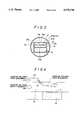
- FIG. 1is a front view, partially in section, of a compound semiconductor vapor phase epitaxial device according to this invention
- FIG. 2is a schematic perspective view, partially broken away, of the epitaxial device of FIG. 1;
- FIG. 3is a sectional view taken along the line III--III in FIG. 1;
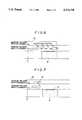
- FIG. 4is a view showing a dispersion of a gas of III group
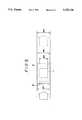
- FIG. 5is a schematic view showing positional relationship of various elements constituting the epitaxial device of FIG. 1;
- FIG. 6is a schematic front view of a modification having a plurality of slits utilized for the device of this invention.
- FIGS. 7 and 8are schematic front views of further modifications in relation to FIG. 6;
- FIG. 9Ais an enlarged perspective view showing a slit in one preferred embodiment
- FIG. 9Bshows a modification of FIG. 9A, in which the slit is replaced with a plurality of fine holes
- FIG. 10shows a modification in which a taper is provided for a first flow channel
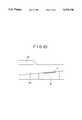
- FIG. 11is a graph showing a positional dependence of the AlGaN alloy composition along the gas flow direction.
- FIGS. 1 to 5A first embodiment of a compound semiconductor vapor phase epitaxial device according to this invention will be first described hereunder with reference to FIGS. 1 to 5.
- a compound semiconductor vapor phase epitaxial device 1called merely an epitaxial device 1 hereinafter, includes a cylindrical reactor vessel 2, first and second flow channels 17 and 27 both accommodated in the reactor vessel 2, and first and second material gas supply pipes 15 and 25 respectively communicated with the first and second flow channels 17 and 27. Both ends of the cylindrical reactor vessel 2 are closed by flanged portions 6 and 16 as end plates. These supply pipes 15 and 25 have first ends inserted into the reactor vessel 2 and communicated with the first and second flow channels 17 and 27, respectively, and have other ends extending outward through the flanged portion 6, and the extended ends of the gas supply pipes 15 and 25 are connected to material gas supply sources 15a and 25a.
- a hydrogen supply pipe 35is further disposed so as to extend into the reactor vessel 2 through the flanged end 6 so as to supply hydrogen gas to outer peripheral areas of the flow channels 17 and 27.
- the hydrogen supply pipe 35is connected to the hydrogen gas supply source 35a.
- To the other flanged end 16is connected a discharge line 30.
- two flow channelsare tightly secured at both longitudinal ends to the end plates 6 and 16 and supported thereby.
- the reactor vessel 2is formed, for example, of quartz material, and an RF coil 3 for heating a susceptor 8 is wound around the outer peripheral portion of the reactor vessel 2.
- the first flow channel 17extends longitudinally in the reactor vessel 2 and has a rectangular cross section defined by four wall structures 17a, 17b, 17c and 17d.
- the upper wall structure 17aforms a lower wall structure of the second flow channel means 27, and the upper wall structure 17a is provided with a slit 10 communicating the first and second flow channels 17 and 27 so that first and second material gases respectively flowing in the first and second channels 17 and 27 are mixed with each other.
- the slit 10has a linearly elongaged hole shape, as shown in FIG.
- the wall structure 17bhas a hollow structure so as to provide a thickness necessary for locating the susceptor 8 on which the crystal substrate 7 is supported.
- the hollow structureis employed, for the purpose of reducing weight and cost, but it may be formed by a solid structure having the required thickness. In both cases, it desired that the surface of the crystal substrate 7 lie at substantially the same level as that of the lower wall structure 17b.
- the lower wall structure 17bhas a ramp portion having an inclination for smoothly guiding the first material gas to the susceptor 8.
- the second channel 27is also defined by four wall structures 27a, 27b, 27c and 27d so as to provide a rectangular cross section and the second channel 27 is disposed above the first flow channel 17, in an installed or operating state, so that the wall structure 27b is commonly formed for the wall structure 17a of the first channel 17.
- the front end, i.e. right-hand end as viewed in FIG. 1, of the second flow channel 27is closed so as to facilitate the gas flow into the first flow channel 17 through the slit 10.
- the first and second flow channels 17 and 27have the same width W3 larger than the width W4 of the susceptor 8 as shown in FIG. 5.
- An excessive amount of the first gasis supplied into the first flow channel 17 and the second gas, which controls the growth rate of the crystal which is formed on the crystal substrate 7, is supplied into the second flow channel 27 positioned adjacent, i.e. above in the installed state, the first flow channel 17.
- the gas supply amounts and the cross sectional areas of the first and second flow channels 17 and 27are determined so that the ratio of flow velocities, that is, flow velocity of the first gas with respect to flow velocity of the second gas, is within 5 to 200, preferably 10 to 100. When this ratio exceeds a value of 200, the switching speed of the second gas is delayed, which results in loss of sharpness of a hetero boundary when a hetero structure is formed and in increased consumption of the first gas.
- the velocity of the first gas flowis generally ranges from 50 to 200 cm/sec.
- NH 3 gas as the first material gas and H 2 gas as a carrier gasare utilized as the first gas excessively supplied into the first flow channel 17, and TMG (trimethylgallium) or a mixed gas of TMG and TMA (trimethylaluminium) as the second material gas and H 2 gas as a carrier gas are utilized as the second gas supplied into the second flow channel 27.
- TMGtrimethylgallium
- TMAtrimethylaluminium
- H 2 S or H 2 Seis preferably utilized as the first material gas supplied into the first flow channel 17 and diethylzinc or dimethylzinc is preferably utilized as the second material gas supplied into the second flow channel 27.
- the H 2 gasis supplied from the hydrogen supply source 35a into the reactor vessel 2 through the hydrogen supply pipe 35, and this H 2 gas performs a sealing function for preventing the material gases from leaking from the first and second flow channels 17 and 27, or it removes the leaking gases if they leak.
- the mixed gas composed of TMG and TMA, being materials of the Group III elements,is also supplied into the second flow channel 27 together with the hydrogen H 2 gas.
- the ratio of concentrationwill be naturally determined as (TMG+TMA concentration) ⁇ (NH 3 concentration), and the flow rate which is determined in consideration of the carrier flow amount and the cross sectional areas of the flow channels, is set to the range in accordance with this invention as described hereinbefore to make the Gas flow rate V1 of the first gas sufficiently large.
- the second gas flowing in the second channel 27can pass the slit 10 formed in the wall section between the first and second channels 17 and 27 as if it were sucked by the first material gas flowing at high velocity in the first channel 17, and thus two-phase flow can be obtained without causing a turbulent flow.
- a laminar flow of the material gasesi.e. a laminar flow rich in the group III material on the side of the slit 10 and a laminar flow rich in the Group V material on the side of the crystal substrate 7 supported by the susceptor 8 is caused on the downstream, right-hand side.
- a laminar gas flow of two or more than two material gasescan be surely formed by suitably utilizing in combination various conditions such as concentrations of the material Gases, Gas flow rate, etc.
- FIG. 6shows a modification in which a plurality of slits 10a are formed, in place of the single slit 10 of FIG. 4, in the wall structure defining the first and second flow channels 17 and 27, and in the illustrated example, four slits 10a are formed extending in a direction normal to the flow direction of the Gases.
- the number of the slits 10amay be determined in consideration of the size of the crystal substrate 7, the working accuracy of the slits 10a and the like.
- FIG. 7shows an alteration in which the downstream end side of the second flow channel 27 is opened, and in this case, a portion of the material Gas flowing in the second flow channel 27 flows downward and into the first flow channel 17 through the slit 10, thus forming the two-phase flow without causing any turbulent flow.
- FIG. 8shows another modification of this invention, in which the second flow channel is divided further into two flow channels 37 and 47, in which slits 30 and 40, each similar to the slit 10, are formed, so as to communicate with the first flow channel 17.
- the Group III TMG and TMAcan be separately fed to the reaction areas through the channels 37 and 47, respectively.
- FIG. 9Bdepicts a further modification of the first embodiment, in which the slit 10 of the first embodiment (FIG. 9A) is replaced with a plurality of fine holes P extending linearly in a direction normal to the flow direction of the gas.
- FIG. 10shows an alteration of the first embodiment, in which the first flow channel 57 has, in an installed state or illustrated state, a lower wall structure which is tapered so as to incline upwardly towards the downstream side of the gas flow to thereby narrow the flow passage of the first channel.
- the composition of the compound semiconductorcan be preferably adjusted uniformly.
- the crystal substratewas first set at a predetermined position in the reactor vessel of the epitaxial device, and thereafter, air in the reactor vessel was vacuum exhausted by means of a rotary vacuum pump, for example, through the discharge line 30 connected to the downstream side of the reactor vessel.
- the NH 3 material gas and the H 2 carrier gaswere supplied into the first flow channel 17 and the TMG and TMA material gases and the H 2 carrier gas were supplied into the second flow channel 27.
- the average flow rate of the gas (NH 3 +H 2 ) passing the first channel 17was set to 110 cm/sec. and the average flow rate of the gas (TMG+TMA+H 2 ) was set to 5.0 cm/sec.
- the temperature of the crystal substrate of 1050° C.was maintained by heating the susceptor 8 by means of the RF coil 3 for one hour to thereby epitaxially grow an AlGaN series compound semiconductor. The positional dependence of the AlGaN alloy composition along the gas flow direction was measured.
- FIG. 11The measured result is shown in FIG. 11, in which the solid line represents the distribution of the experiment according to this invention.
- the distribution of a mixed crystal ratio according to a prior art device in which no flow channel is utilized, a so called normal pressure type MOCVD deviceis also in FIG. 11 by a dotted line.
- the composition of the film-formed crystal formed on the crystal substratecan be made substantially uniform and the reproducibility can be also improved.
Landscapes
- Chemical & Material Sciences (AREA)
- General Chemical & Material Sciences (AREA)
- Chemical Kinetics & Catalysis (AREA)
- Engineering & Computer Science (AREA)
- Materials Engineering (AREA)
- Metallurgy (AREA)
- Organic Chemistry (AREA)
- Mechanical Engineering (AREA)
- Crystallography & Structural Chemistry (AREA)
Abstract
Description
Claims (12)
Applications Claiming Priority (2)
| Application Number | Priority Date | Filing Date | Title |
|---|---|---|---|
| JP04049711AJP3131005B2 (en) | 1992-03-06 | 1992-03-06 | Compound semiconductor vapor deposition equipment |
| JP4-049711 | 1992-03-06 |
Publications (1)
| Publication Number | Publication Date |
|---|---|
| US5370738Atrue US5370738A (en) | 1994-12-06 |
Family
ID=12838776
Family Applications (1)
| Application Number | Title | Priority Date | Filing Date |
|---|---|---|---|
| US08/012,780Expired - Fee RelatedUS5370738A (en) | 1992-03-06 | 1993-02-03 | Compound semiconductor vapor phase epitaxial device |
Country Status (4)
| Country | Link |
|---|---|
| US (1) | US5370738A (en) |
| EP (1) | EP0559326B1 (en) |
| JP (1) | JP3131005B2 (en) |
| DE (1) | DE69310422T2 (en) |
Cited By (43)
| Publication number | Priority date | Publication date | Assignee | Title |
|---|---|---|---|---|
| US5749974A (en)* | 1994-07-15 | 1998-05-12 | Shin-Etsu Handotai Co., Ltd. | Method of chemical vapor deposition and reactor therefor |
| US5821175A (en)* | 1988-07-08 | 1998-10-13 | Cauldron Limited Partnership | Removal of surface contaminants by irradiation using various methods to achieve desired inert gas flow over treated surface |
| US5891251A (en)* | 1996-08-07 | 1999-04-06 | Macleish; Joseph H. | CVD reactor having heated process chamber within isolation chamber |
| US6090211A (en)* | 1996-03-27 | 2000-07-18 | Matsushita Electric Industrial Co., Ltd. | Apparatus and method for forming semiconductor thin layer |
| US6093252A (en)* | 1995-08-03 | 2000-07-25 | Asm America, Inc. | Process chamber with inner support |
| US6113984A (en)* | 1996-08-07 | 2000-09-05 | Concept Systems Design, Inc. | Gas injection system for CVD reactors |
| US6190457B1 (en)* | 1996-03-22 | 2001-02-20 | Nippon Sanso Corporation | CVD system and CVD process |
| US20020041931A1 (en)* | 1994-11-28 | 2002-04-11 | Tuomo Suntola | Method for growing thin films |
| US6383330B1 (en) | 1999-09-10 | 2002-05-07 | Asm America, Inc. | Quartz wafer processing chamber |
| US20030075273A1 (en)* | 2001-08-15 | 2003-04-24 | Olli Kilpela | Atomic layer deposition reactor |
| US20030150560A1 (en)* | 2002-02-08 | 2003-08-14 | Kinnard David William | Reactor assembly and processing method |
| US6666921B2 (en)* | 2001-02-28 | 2003-12-23 | Japan Pionics Co., Ltd. | Chemical vapor deposition apparatus and chemical vapor deposition method |
| US20040009307A1 (en)* | 2000-06-08 | 2004-01-15 | Won-Yong Koh | Thin film forming method |
| US20050221618A1 (en)* | 2004-03-31 | 2005-10-06 | Amrhein Frederick J | System for controlling a plenum output flow geometry |
| US20060057824A1 (en)* | 2004-09-10 | 2006-03-16 | Masahiro Araki | Apparatus for producing nitride semiconductor, method for producing nitride semiconductor, and semiconductor laser device obtained by the method |
| US20060249077A1 (en)* | 2005-05-09 | 2006-11-09 | Kim Daeyoun | Multiple inlet atomic layer deposition reactor |
| US20080110399A1 (en)* | 2006-11-09 | 2008-05-15 | Asm Genitech Korea Ltd. | Atomic layer deposition apparatus |
| US20080131979A1 (en)* | 2006-12-04 | 2008-06-05 | Sumitomo Electric Industries, Ltd. | Vapor-Phase Growth System and Vapor-Phase Growth Method |
| US20080241387A1 (en)* | 2007-03-29 | 2008-10-02 | Asm International N.V. | Atomic layer deposition reactor |
| US20080241384A1 (en)* | 2007-04-02 | 2008-10-02 | Asm Genitech Korea Ltd. | Lateral flow deposition apparatus and method of depositing film by using the apparatus |
| US20080248200A1 (en)* | 2005-06-02 | 2008-10-09 | Asm America, Inc. | Apparatus and methods for isolating chemical vapor reactions at a substrate surface |
| US20090136665A1 (en)* | 2007-11-27 | 2009-05-28 | Asm Genitech Korea Ltd. | Atomic layer deposition apparatus |
| US20090197402A1 (en)* | 2008-01-31 | 2009-08-06 | Hitachi Kokusai Electric, Inc. | Substrate processing apparatus, method for manufacturing semiconductor device, and process tube |
| US20090229519A1 (en)* | 2005-12-21 | 2009-09-17 | Hiroaki Saitoh | Apparatus for manufacturing semiconductor thin film |
| US20100266765A1 (en)* | 2009-04-21 | 2010-10-21 | White Carl L | Method and apparatus for growing a thin film onto a substrate |
| US20100307418A1 (en)* | 2009-06-09 | 2010-12-09 | Japan Pionics., Ltd. | Vapor phase epitaxy apparatus of group iii nitride semiconductor |
| US20110117729A1 (en)* | 2009-11-18 | 2011-05-19 | Rec Silicon Inc | Fluid bed reactor |
| US20120266819A1 (en)* | 2011-04-25 | 2012-10-25 | Applied Materials, Inc. | Semiconductor substrate processing system |
| US20120266821A1 (en)* | 2005-01-18 | 2012-10-25 | Asm America, Inc. | Reaction system for growing a thin film |
| US8383525B2 (en) | 2008-04-25 | 2013-02-26 | Asm America, Inc. | Plasma-enhanced deposition process for forming a metal oxide thin film and related structures |
| TWI480414B (en)* | 2012-11-14 | 2015-04-11 | Ind Tech Res Inst | Gas injection system and vapor phase epitaxial device |
| US20150140791A1 (en)* | 2011-05-31 | 2015-05-21 | Hitachi Metals, Ltd. | Apparatus for producing metal chloride gas and method for producing metal chloride gas, and apparatus for hydride vapor phase epitaxy, nitride semiconductor wafer, nitride semiconductor device, wafer for nitride semiconductor light emitting diode, method for manufacturing nitride semiconductor freestanidng substrate and nitride semiconductor crystal |
| US20150167161A1 (en)* | 2012-06-07 | 2015-06-18 | Soitec | Gas injection components for deposition systems and related methods |
| TWI494461B (en)* | 2011-08-22 | 2015-08-01 | Soitec Silicon On Insulator | Deposition systems including a precursor gas furnace within a reaction chamber, and related methods |
| US20150345046A1 (en)* | 2012-12-27 | 2015-12-03 | Showa Denko K.K. | Film-forming device |
| US20160194753A1 (en)* | 2012-12-27 | 2016-07-07 | Showa Denko K.K. | SiC-FILM FORMATION DEVICE AND METHOD FOR PRODUCING SiC FILM |
| US9644285B2 (en) | 2011-08-22 | 2017-05-09 | Soitec | Direct liquid injection for halide vapor phase epitaxy systems and methods |
| US10358743B2 (en) | 2009-08-12 | 2019-07-23 | Georgia State University Research Foundation, Inc. | High pressure chemical vapor deposition apparatuses, methods, and compositions produced therewith |
| US10619240B2 (en)* | 2017-08-16 | 2020-04-14 | Wuhan China Star Optoelectronics Semiconductor Display Technology Co., Ltd. | Gas diffusion device and film-forming apparatus |
| US10872804B2 (en) | 2017-11-03 | 2020-12-22 | Asm Ip Holding B.V. | Apparatus and methods for isolating a reaction chamber from a loading chamber resulting in reduced contamination |
| US10872803B2 (en) | 2017-11-03 | 2020-12-22 | Asm Ip Holding B.V. | Apparatus and methods for isolating a reaction chamber from a loading chamber resulting in reduced contamination |
| US11032945B2 (en)* | 2019-07-12 | 2021-06-08 | Applied Materials, Inc. | Heat shield assembly for an epitaxy chamber |
| CN118335583A (en)* | 2024-04-09 | 2024-07-12 | 上海谙邦半导体设备有限公司 | Air intake device and semiconductor processing equipment including the same |
Families Citing this family (20)
| Publication number | Priority date | Publication date | Assignee | Title |
|---|---|---|---|---|
| JP3042335B2 (en)* | 1994-10-25 | 2000-05-15 | 信越半導体株式会社 | Vapor phase growth method and apparatus |
| FI97731C (en)* | 1994-11-28 | 1997-02-10 | Mikrokemia Oy | Method and apparatus for making thin films |
| FI97730C (en)* | 1994-11-28 | 1997-02-10 | Mikrokemia Oy | Apparatus for making thin films |
| IL118850A0 (en) | 1996-07-14 | 1996-10-31 | Orziv Ltd | Device and method for laser marking |
| JPH1154442A (en)* | 1997-08-07 | 1999-02-26 | Shin Etsu Handotai Co Ltd | Manufacture of compound semiconductor epitaxial wafer and vapor-phase growth device used for the same |
| AU4596500A (en)* | 1999-05-13 | 2000-12-05 | Emf Ireland Limited | Method and apparatus for epitaxially growing a material on substrate |
| JP4588894B2 (en)* | 2001-01-31 | 2010-12-01 | 信越半導体株式会社 | Vapor phase growth apparatus and epitaxial wafer manufacturing method |
| JP2002371361A (en)* | 2001-06-18 | 2002-12-26 | Japan Pionics Co Ltd | Vapor phase growth apparatus and vapor phase growth method |
| US6800134B2 (en) | 2002-03-26 | 2004-10-05 | Micron Technology, Inc. | Chemical vapor deposition methods and atomic layer deposition methods |
| DE10320597A1 (en)* | 2003-04-30 | 2004-12-02 | Aixtron Ag | Method and device for depositing semiconductor layers with two process gases, one of which is preconditioned |
| JP4598568B2 (en)* | 2005-03-09 | 2010-12-15 | 大陽日酸株式会社 | Vapor growth equipment |
| JP4193883B2 (en) | 2006-07-05 | 2008-12-10 | 住友電気工業株式会社 | Metalorganic vapor phase epitaxy system |
| JP2008034780A (en)* | 2006-07-07 | 2008-02-14 | Fuji Electric Holdings Co Ltd | Manufacturing method of semiconductor SiC substrate with epitaxial SiC film and epitaxial SiC film forming apparatus thereof |
| JP5064132B2 (en)* | 2007-07-25 | 2012-10-31 | シャープ株式会社 | Vapor growth apparatus and method for manufacturing semiconductor device |
| JP4466723B2 (en) | 2007-11-21 | 2010-05-26 | 住友電気工業株式会社 | Metalorganic vapor phase epitaxy system |
| CN101849042B (en)* | 2007-12-20 | 2014-06-18 | 硅绝缘体技术有限公司 | Apparatus for delivering precursor gases to an epitaxial growth substrate |
| WO2012127305A1 (en)* | 2011-03-21 | 2012-09-27 | Centrotherm Photovoltaics Ag | Gas supply for a processing furnace |
| DE102016101003A1 (en) | 2016-01-21 | 2017-07-27 | Aixtron Se | CVD apparatus with a process chamber housing which can be removed from the reactor housing as an assembly |
| KR102564228B1 (en)* | 2021-04-29 | 2023-08-09 | 주식회사 테스 | Metal organic chemical vapor deposition apparatus |
| JPWO2023175826A1 (en)* | 2022-03-17 | 2023-09-21 |
Citations (13)
| Publication number | Priority date | Publication date | Assignee | Title |
|---|---|---|---|---|
| US4533410A (en)* | 1982-10-19 | 1985-08-06 | Matsushita Electric Industrial Co., Ltd. | Process of vapor phase epitaxy of compound semiconductors |
| JPS61186288A (en)* | 1985-02-14 | 1986-08-19 | Nec Corp | Apparatus for vapor-phase epitaxial growth of silicon carbide compound semiconductor |
| US4731255A (en)* | 1984-09-26 | 1988-03-15 | Applied Materials Japan, Inc. | Gas-phase growth process and an apparatus for the same |
| EP0282075A2 (en)* | 1987-03-12 | 1988-09-14 | Sumitomo Electric Industries Limited | Thin film single crystal substrate |
| US4808551A (en)* | 1986-02-14 | 1989-02-28 | Nippon Telegraph & Telephone Corporation | Method for halide VPE of III-V compound semiconductors |
| JPH01136971A (en)* | 1987-11-20 | 1989-05-30 | Fujitsu Ltd | Vapor phase growth equipment |
| GB2220957A (en)* | 1988-07-15 | 1990-01-24 | Mitsubishi Electric Corp | Thin film forming apparatus |
| FR2661554A1 (en)* | 1990-04-30 | 1991-10-31 | Philips Electronique Lab | Device for introducing gases into the chamber of an epitaxy reactor, reactor chamber including such a gas-introduction device, and use of such a chamber for producing semiconducting layers |
| JPH03250623A (en)* | 1990-02-28 | 1991-11-08 | Nec Corp | Vapor growing method for iii-v compound semiconductor |
| US5070814A (en)* | 1987-12-22 | 1991-12-10 | U.S. Philips Corporation | Cvd reactor vessel for forming a solid state electronic device |
| EP0505249A1 (en)* | 1991-03-18 | 1992-09-23 | Fujitsu Limited | Apparatus for growing mixed compound semiconductor and growth method using the same |
| US5183510A (en)* | 1988-11-30 | 1993-02-02 | Fujitsu Limited | Apparatus and process for chemical vapor deposition |
| US5254210A (en)* | 1992-04-27 | 1993-10-19 | The United States Of America As Represented By The Secretary Of The Army | Method and apparatus for growing semiconductor heterostructures |
- 1992
- 1992-03-06JPJP04049711Apatent/JP3131005B2/ennot_activeExpired - Fee Related
- 1993
- 1993-02-01EPEP93300724Apatent/EP0559326B1/ennot_activeExpired - Lifetime
- 1993-02-01DEDE69310422Tpatent/DE69310422T2/ennot_activeExpired - Fee Related
- 1993-02-03USUS08/012,780patent/US5370738A/ennot_activeExpired - Fee Related
Patent Citations (13)
| Publication number | Priority date | Publication date | Assignee | Title |
|---|---|---|---|---|
| US4533410A (en)* | 1982-10-19 | 1985-08-06 | Matsushita Electric Industrial Co., Ltd. | Process of vapor phase epitaxy of compound semiconductors |
| US4731255A (en)* | 1984-09-26 | 1988-03-15 | Applied Materials Japan, Inc. | Gas-phase growth process and an apparatus for the same |
| JPS61186288A (en)* | 1985-02-14 | 1986-08-19 | Nec Corp | Apparatus for vapor-phase epitaxial growth of silicon carbide compound semiconductor |
| US4808551A (en)* | 1986-02-14 | 1989-02-28 | Nippon Telegraph & Telephone Corporation | Method for halide VPE of III-V compound semiconductors |
| EP0282075A2 (en)* | 1987-03-12 | 1988-09-14 | Sumitomo Electric Industries Limited | Thin film single crystal substrate |
| JPH01136971A (en)* | 1987-11-20 | 1989-05-30 | Fujitsu Ltd | Vapor phase growth equipment |
| US5070814A (en)* | 1987-12-22 | 1991-12-10 | U.S. Philips Corporation | Cvd reactor vessel for forming a solid state electronic device |
| GB2220957A (en)* | 1988-07-15 | 1990-01-24 | Mitsubishi Electric Corp | Thin film forming apparatus |
| US5183510A (en)* | 1988-11-30 | 1993-02-02 | Fujitsu Limited | Apparatus and process for chemical vapor deposition |
| JPH03250623A (en)* | 1990-02-28 | 1991-11-08 | Nec Corp | Vapor growing method for iii-v compound semiconductor |
| FR2661554A1 (en)* | 1990-04-30 | 1991-10-31 | Philips Electronique Lab | Device for introducing gases into the chamber of an epitaxy reactor, reactor chamber including such a gas-introduction device, and use of such a chamber for producing semiconducting layers |
| EP0505249A1 (en)* | 1991-03-18 | 1992-09-23 | Fujitsu Limited | Apparatus for growing mixed compound semiconductor and growth method using the same |
| US5254210A (en)* | 1992-04-27 | 1993-10-19 | The United States Of America As Represented By The Secretary Of The Army | Method and apparatus for growing semiconductor heterostructures |
Cited By (70)
| Publication number | Priority date | Publication date | Assignee | Title |
|---|---|---|---|---|
| US5821175A (en)* | 1988-07-08 | 1998-10-13 | Cauldron Limited Partnership | Removal of surface contaminants by irradiation using various methods to achieve desired inert gas flow over treated surface |
| US5749974A (en)* | 1994-07-15 | 1998-05-12 | Shin-Etsu Handotai Co., Ltd. | Method of chemical vapor deposition and reactor therefor |
| US6254933B1 (en) | 1994-07-15 | 2001-07-03 | Shin-Etsu Handotai, Ltd. | Method of chemical vapor deposition |
| US8507039B2 (en) | 1994-11-28 | 2013-08-13 | Asm America, Inc. | Method for growing thin films |
| US20080138518A1 (en)* | 1994-11-28 | 2008-06-12 | Tuomo Suntola | Method for growing thin films |
| US7404984B2 (en) | 1994-11-28 | 2008-07-29 | Asm America, Inc. | Method for growing thin films |
| US7498059B2 (en) | 1994-11-28 | 2009-03-03 | Asm America, Inc. | Method for growing thin films |
| US20090181169A1 (en)* | 1994-11-28 | 2009-07-16 | Asm America, Inc. | Method for growing thin films |
| US20020041931A1 (en)* | 1994-11-28 | 2002-04-11 | Tuomo Suntola | Method for growing thin films |
| US6572705B1 (en)* | 1994-11-28 | 2003-06-03 | Asm America, Inc. | Method and apparatus for growing thin films |
| US6608287B2 (en) | 1995-08-03 | 2003-08-19 | Asm America, Inc. | Process chamber with rectangular temperature compensation ring |
| US6464792B1 (en) | 1995-08-03 | 2002-10-15 | Asm America, Inc. | Process chamber with downstream getter plate |
| US6093252A (en)* | 1995-08-03 | 2000-07-25 | Asm America, Inc. | Process chamber with inner support |
| US6190457B1 (en)* | 1996-03-22 | 2001-02-20 | Nippon Sanso Corporation | CVD system and CVD process |
| US6090211A (en)* | 1996-03-27 | 2000-07-18 | Matsushita Electric Industrial Co., Ltd. | Apparatus and method for forming semiconductor thin layer |
| US6113984A (en)* | 1996-08-07 | 2000-09-05 | Concept Systems Design, Inc. | Gas injection system for CVD reactors |
| US5891251A (en)* | 1996-08-07 | 1999-04-06 | Macleish; Joseph H. | CVD reactor having heated process chamber within isolation chamber |
| US6540837B2 (en) | 1999-09-10 | 2003-04-01 | Asm America, Inc. | Quartz wafer processing chamber |
| US6383330B1 (en) | 1999-09-10 | 2002-05-07 | Asm America, Inc. | Quartz wafer processing chamber |
| US7141278B2 (en) | 2000-06-08 | 2006-11-28 | Asm Genitech Korea Ltd. | Thin film forming method |
| US20040009307A1 (en)* | 2000-06-08 | 2004-01-15 | Won-Yong Koh | Thin film forming method |
| US7485349B2 (en) | 2000-06-08 | 2009-02-03 | Asm Genitech Korea Ltd. | Thin film forming method |
| US20070048455A1 (en)* | 2000-06-08 | 2007-03-01 | Asm Genitech Korea Ltd. | Thin film forming method |
| US6666921B2 (en)* | 2001-02-28 | 2003-12-23 | Japan Pionics Co., Ltd. | Chemical vapor deposition apparatus and chemical vapor deposition method |
| US20050092249A1 (en)* | 2001-08-15 | 2005-05-05 | Olli Kilpela | Atomic layer deposition reactor |
| US20030075273A1 (en)* | 2001-08-15 | 2003-04-24 | Olli Kilpela | Atomic layer deposition reactor |
| US6820570B2 (en)* | 2001-08-15 | 2004-11-23 | Nobel Biocare Services Ag | Atomic layer deposition reactor |
| US20030150560A1 (en)* | 2002-02-08 | 2003-08-14 | Kinnard David William | Reactor assembly and processing method |
| US7163587B2 (en)* | 2002-02-08 | 2007-01-16 | Axcelis Technologies, Inc. | Reactor assembly and processing method |
| US20050221618A1 (en)* | 2004-03-31 | 2005-10-06 | Amrhein Frederick J | System for controlling a plenum output flow geometry |
| US20060057824A1 (en)* | 2004-09-10 | 2006-03-16 | Masahiro Araki | Apparatus for producing nitride semiconductor, method for producing nitride semiconductor, and semiconductor laser device obtained by the method |
| US20120266821A1 (en)* | 2005-01-18 | 2012-10-25 | Asm America, Inc. | Reaction system for growing a thin film |
| US10468291B2 (en) | 2005-01-18 | 2019-11-05 | Asm America, Inc. | Reaction system for growing a thin film |
| US9359672B2 (en)* | 2005-01-18 | 2016-06-07 | Asm America, Inc. | Reaction system for growing a thin film |
| US20060249077A1 (en)* | 2005-05-09 | 2006-11-09 | Kim Daeyoun | Multiple inlet atomic layer deposition reactor |
| KR101272321B1 (en)* | 2005-05-09 | 2013-06-07 | 한국에이에스엠지니텍 주식회사 | Multiple inlet atomic layer deposition reactor |
| US20080248200A1 (en)* | 2005-06-02 | 2008-10-09 | Asm America, Inc. | Apparatus and methods for isolating chemical vapor reactions at a substrate surface |
| US20090229519A1 (en)* | 2005-12-21 | 2009-09-17 | Hiroaki Saitoh | Apparatus for manufacturing semiconductor thin film |
| US20080110399A1 (en)* | 2006-11-09 | 2008-05-15 | Asm Genitech Korea Ltd. | Atomic layer deposition apparatus |
| US20080131979A1 (en)* | 2006-12-04 | 2008-06-05 | Sumitomo Electric Industries, Ltd. | Vapor-Phase Growth System and Vapor-Phase Growth Method |
| US20080241387A1 (en)* | 2007-03-29 | 2008-10-02 | Asm International N.V. | Atomic layer deposition reactor |
| US20080241384A1 (en)* | 2007-04-02 | 2008-10-02 | Asm Genitech Korea Ltd. | Lateral flow deposition apparatus and method of depositing film by using the apparatus |
| US20090136665A1 (en)* | 2007-11-27 | 2009-05-28 | Asm Genitech Korea Ltd. | Atomic layer deposition apparatus |
| US8282735B2 (en)* | 2007-11-27 | 2012-10-09 | Asm Genitech Korea Ltd. | Atomic layer deposition apparatus |
| US8545940B2 (en) | 2007-11-27 | 2013-10-01 | Asm Genitech Korea Ltd. | Atomic layer deposition apparatus |
| US20090197402A1 (en)* | 2008-01-31 | 2009-08-06 | Hitachi Kokusai Electric, Inc. | Substrate processing apparatus, method for manufacturing semiconductor device, and process tube |
| US8303712B2 (en)* | 2008-01-31 | 2012-11-06 | Hitachi Kokusai Electric Inc. | Substrate processing apparatus, method for manufacturing semiconductor device, and process tube |
| US8383525B2 (en) | 2008-04-25 | 2013-02-26 | Asm America, Inc. | Plasma-enhanced deposition process for forming a metal oxide thin film and related structures |
| US20100266765A1 (en)* | 2009-04-21 | 2010-10-21 | White Carl L | Method and apparatus for growing a thin film onto a substrate |
| CN101924023A (en)* | 2009-06-09 | 2010-12-22 | 日本派欧尼株式会社 | Vapor Phase Growth Apparatus for Group III Nitride Semiconductors |
| US20100307418A1 (en)* | 2009-06-09 | 2010-12-09 | Japan Pionics., Ltd. | Vapor phase epitaxy apparatus of group iii nitride semiconductor |
| US10358743B2 (en) | 2009-08-12 | 2019-07-23 | Georgia State University Research Foundation, Inc. | High pressure chemical vapor deposition apparatuses, methods, and compositions produced therewith |
| US20110117729A1 (en)* | 2009-11-18 | 2011-05-19 | Rec Silicon Inc | Fluid bed reactor |
| US9023425B2 (en) | 2009-11-18 | 2015-05-05 | Rec Silicon Inc | Fluid bed reactor |
| US8075692B2 (en)* | 2009-11-18 | 2011-12-13 | Rec Silicon Inc | Fluid bed reactor |
| US20120266819A1 (en)* | 2011-04-25 | 2012-10-25 | Applied Materials, Inc. | Semiconductor substrate processing system |
| US9512520B2 (en)* | 2011-04-25 | 2016-12-06 | Applied Materials, Inc. | Semiconductor substrate processing system |
| US20150140791A1 (en)* | 2011-05-31 | 2015-05-21 | Hitachi Metals, Ltd. | Apparatus for producing metal chloride gas and method for producing metal chloride gas, and apparatus for hydride vapor phase epitaxy, nitride semiconductor wafer, nitride semiconductor device, wafer for nitride semiconductor light emitting diode, method for manufacturing nitride semiconductor freestanidng substrate and nitride semiconductor crystal |
| US9644285B2 (en) | 2011-08-22 | 2017-05-09 | Soitec | Direct liquid injection for halide vapor phase epitaxy systems and methods |
| TWI494461B (en)* | 2011-08-22 | 2015-08-01 | Soitec Silicon On Insulator | Deposition systems including a precursor gas furnace within a reaction chamber, and related methods |
| US20150167161A1 (en)* | 2012-06-07 | 2015-06-18 | Soitec | Gas injection components for deposition systems and related methods |
| TWI480414B (en)* | 2012-11-14 | 2015-04-11 | Ind Tech Res Inst | Gas injection system and vapor phase epitaxial device |
| US20160194753A1 (en)* | 2012-12-27 | 2016-07-07 | Showa Denko K.K. | SiC-FILM FORMATION DEVICE AND METHOD FOR PRODUCING SiC FILM |
| US20150345046A1 (en)* | 2012-12-27 | 2015-12-03 | Showa Denko K.K. | Film-forming device |
| US10619240B2 (en)* | 2017-08-16 | 2020-04-14 | Wuhan China Star Optoelectronics Semiconductor Display Technology Co., Ltd. | Gas diffusion device and film-forming apparatus |
| US10872804B2 (en) | 2017-11-03 | 2020-12-22 | Asm Ip Holding B.V. | Apparatus and methods for isolating a reaction chamber from a loading chamber resulting in reduced contamination |
| US10872803B2 (en) | 2017-11-03 | 2020-12-22 | Asm Ip Holding B.V. | Apparatus and methods for isolating a reaction chamber from a loading chamber resulting in reduced contamination |
| US11626313B2 (en) | 2017-11-03 | 2023-04-11 | Asm Ip Holding B.V. | Apparatus and methods for isolating a reaction chamber from a loading chamber resulting in reduced contamination |
| US11032945B2 (en)* | 2019-07-12 | 2021-06-08 | Applied Materials, Inc. | Heat shield assembly for an epitaxy chamber |
| CN118335583A (en)* | 2024-04-09 | 2024-07-12 | 上海谙邦半导体设备有限公司 | Air intake device and semiconductor processing equipment including the same |
Also Published As
| Publication number | Publication date |
|---|---|
| EP0559326B1 (en) | 1997-05-07 |
| JPH06216030A (en) | 1994-08-05 |
| EP0559326A1 (en) | 1993-09-08 |
| DE69310422T2 (en) | 1997-11-06 |
| DE69310422D1 (en) | 1997-06-12 |
| JP3131005B2 (en) | 2001-01-31 |
Similar Documents
| Publication | Publication Date | Title |
|---|---|---|
| US5370738A (en) | Compound semiconductor vapor phase epitaxial device | |
| US4980204A (en) | Metal organic chemical vapor deposition method with controlled gas flow rate | |
| US10364509B2 (en) | Alkyl push flow for vertical flow rotating disk reactors | |
| EP1432844B1 (en) | Apparatus for inverted cvd | |
| EP0837495B1 (en) | Vapor phase growth apparatus | |
| JP4193883B2 (en) | Metalorganic vapor phase epitaxy system | |
| US5254210A (en) | Method and apparatus for growing semiconductor heterostructures | |
| TW389940B (en) | Manufacturing method of compound semiconductor epitaxial wafer and vapor-phase growth device | |
| JP2976972B1 (en) | Gas rectifier | |
| US20020195054A1 (en) | Method and apparatus for depositing semiconductor film and method for fabricating semiconductor device | |
| US5229319A (en) | Method for producing compound semiconductors and apparatus therefor | |
| CN101535523B (en) | Density Matched Alkyl Extrusion Flow for Vertical Flow Rotating Disk Reactors | |
| JP2988949B2 (en) | Metalorganic vapor phase epitaxy | |
| JP3472976B2 (en) | Method and apparatus for forming group III nitride semiconductor | |
| Blaauw et al. | A gas mixing device for MOCVD | |
| JPH11329980A (en) | Metal organic chemical vapor deposition apparatus and metal organic chemical vapor deposition method using the same | |
| JP3112445B2 (en) | Gallium nitride based compound semiconductor vapor phase growth equipment | |
| JPH02126632A (en) | Vapor phase epitaxy for compound semiconductor crystal layer and reaction tube therefor | |
| EP0171242A2 (en) | Methods of making semiconductor light-emitting devices and vapour phase growth apparatus used for carrying out the methods | |
| JPH08130187A (en) | Semiconductor vapor phase growth apparatus and semiconductor vapor phase growth method | |
| JPH10256166A (en) | Vapor phase growth apparatus and vapor phase growth method | |
| JPS60176992A (en) | Device for gaseous phase epitaxial growth of organometallic compound | |
| JPH01283918A (en) | Optical vapor growth apparatus | |
| JPH0551559B2 (en) |
Legal Events
| Date | Code | Title | Description |
|---|---|---|---|
| AS | Assignment | Owner name:AKASAKI, ISAMU, JAPAN Free format text:ASSIGNMENT OF ASSIGNORS INTEREST.;ASSIGNORS:WATANABE, ATSUSHI;HIRAMATSU, KAZUMASA;REEL/FRAME:006463/0896 Effective date:19921124 Owner name:AMANO, HIROSHI, JAPAN Free format text:ASSIGNMENT OF ASSIGNORS INTEREST.;ASSIGNORS:WATANABE, ATSUSHI;HIRAMATSU, KAZUMASA;REEL/FRAME:006463/0896 Effective date:19921124 Owner name:PIONEER ELECTRONIC CORPORATION, JAPAN Free format text:ASSIGNMENT OF ASSIGNORS INTEREST.;ASSIGNORS:WATANABE, ATSUSHI;HIRAMATSU, KAZUMASA;REEL/FRAME:006463/0896 Effective date:19921124 | |
| FEPP | Fee payment procedure | Free format text:PAYOR NUMBER ASSIGNED (ORIGINAL EVENT CODE: ASPN); ENTITY STATUS OF PATENT OWNER: LARGE ENTITY | |
| FPAY | Fee payment | Year of fee payment:4 | |
| FPAY | Fee payment | Year of fee payment:8 | |
| REMI | Maintenance fee reminder mailed | ||
| FEPP | Fee payment procedure | Free format text:PAYER NUMBER DE-ASSIGNED (ORIGINAL EVENT CODE: RMPN); ENTITY STATUS OF PATENT OWNER: LARGE ENTITY | |
| REMI | Maintenance fee reminder mailed | ||
| LAPS | Lapse for failure to pay maintenance fees | ||
| STCH | Information on status: patent discontinuation | Free format text:PATENT EXPIRED DUE TO NONPAYMENT OF MAINTENANCE FEES UNDER 37 CFR 1.362 | |
| FP | Lapsed due to failure to pay maintenance fee | Effective date:20061206 |