US5364803A - Method of preventing fluorine-induced gate oxide degradation in WSix polycide structure - Google Patents
Method of preventing fluorine-induced gate oxide degradation in WSix polycide structureDownload PDFInfo
- Publication number
- US5364803A US5364803AUS08/080,304US8030493AUS5364803AUS 5364803 AUS5364803 AUS 5364803AUS 8030493 AUS8030493 AUS 8030493AUS 5364803 AUS5364803 AUS 5364803A
- Authority
- US
- United States
- Prior art keywords
- layer
- diffusion barrier
- gate
- thin conducting
- tungsten silicide
- Prior art date
- Legal status (The legal status is an assumption and is not a legal conclusion. Google has not performed a legal analysis and makes no representation as to the accuracy of the status listed.)
- Expired - Lifetime
Links
- 230000015556catabolic processEffects0.000titleclaimsabstractdescription8
- 238000006731degradation reactionMethods0.000titleclaimsabstractdescription8
- 238000000034methodMethods0.000titleclaimsdescription19
- 229910052731fluorineInorganic materials0.000titleclaimsdescription10
- YCKRFDGAMUMZLT-UHFFFAOYSA-NFluorine atomChemical compound[F]YCKRFDGAMUMZLT-UHFFFAOYSA-N0.000titleclaimsdescription9
- 239000011737fluorineSubstances0.000titleclaimsdescription9
- 238000009792diffusion processMethods0.000claimsabstractdescription32
- WQJQOUPTWCFRMM-UHFFFAOYSA-Ntungsten disilicideChemical compound[Si]#[W]#[Si]WQJQOUPTWCFRMM-UHFFFAOYSA-N0.000claimsabstractdescription30
- 229910021342tungsten silicideInorganic materials0.000claimsabstractdescription30
- 230000004888barrier functionEffects0.000claimsabstractdescription29
- 229910021420polycrystalline siliconInorganic materials0.000claimsabstractdescription26
- 229920005591polysiliconPolymers0.000claimsabstractdescription25
- 125000001153fluoro groupChemical groupF*0.000claimsabstractdescription22
- 239000000758substrateSubstances0.000claimsabstractdescription9
- 238000004519manufacturing processMethods0.000claimsabstractdescription8
- 239000004065semiconductorSubstances0.000claimsabstractdescription6
- 230000015572biosynthetic processEffects0.000claimsabstractdescription5
- 230000008021depositionEffects0.000claimsabstractdescription5
- 239000012495reaction gasSubstances0.000claimsabstractdescription4
- 238000000151depositionMethods0.000claimsdescription9
- VYPSYNLAJGMNEJ-UHFFFAOYSA-NSilicium dioxideChemical compoundO=[Si]=OVYPSYNLAJGMNEJ-UHFFFAOYSA-N0.000claimsdescription6
- 229910052814silicon oxideInorganic materials0.000claimsdescription6
- NRTOMJZYCJJWKI-UHFFFAOYSA-NTitanium nitrideChemical compound[Ti]#NNRTOMJZYCJJWKI-UHFFFAOYSA-N0.000claimsdescription5
- 238000000137annealingMethods0.000claimsdescription5
- RTAQQCXQSZGOHL-UHFFFAOYSA-NTitaniumChemical compound[Ti]RTAQQCXQSZGOHL-UHFFFAOYSA-N0.000claimsdescription4
- MZLGASXMSKOWSE-UHFFFAOYSA-Ntantalum nitrideChemical compound[Ta]#NMZLGASXMSKOWSE-UHFFFAOYSA-N0.000claimsdescription3
- 239000010936titaniumSubstances0.000claimsdescription3
- 229910052719titaniumInorganic materials0.000claimsdescription3
- WFKWXMTUELFFGS-UHFFFAOYSA-NtungstenChemical compound[W]WFKWXMTUELFFGS-UHFFFAOYSA-N0.000claimsdescription3
- 229910052721tungstenInorganic materials0.000claimsdescription3
- 239000010937tungstenSubstances0.000claimsdescription3
- 238000005137deposition processMethods0.000claimsdescription2
- 238000000059patterningMethods0.000claims2
- KRHYYFGTRYWZRS-UHFFFAOYSA-MFluoride anionChemical compound[F-]KRHYYFGTRYWZRS-UHFFFAOYSA-M0.000claims1
- 229910010421TiNxInorganic materials0.000description5
- QVGXLLKOCUKJST-UHFFFAOYSA-Natomic oxygenChemical compound[O]QVGXLLKOCUKJST-UHFFFAOYSA-N0.000description3
- 229910052760oxygenInorganic materials0.000description3
- 239000001301oxygenSubstances0.000description3
- OAICVXFJPJFONN-UHFFFAOYSA-NPhosphorusChemical compound[P]OAICVXFJPJFONN-UHFFFAOYSA-N0.000description2
- BLRPTPMANUNPDV-UHFFFAOYSA-NSilaneChemical compound[SiH4]BLRPTPMANUNPDV-UHFFFAOYSA-N0.000description2
- XUIMIQQOPSSXEZ-UHFFFAOYSA-NSiliconChemical compound[Si]XUIMIQQOPSSXEZ-UHFFFAOYSA-N0.000description2
- 229910052785arsenicInorganic materials0.000description2
- -1arsenic ionsChemical class0.000description2
- 238000006243chemical reactionMethods0.000description2
- 238000005530etchingMethods0.000description2
- 239000007789gasSubstances0.000description2
- 239000012535impuritySubstances0.000description2
- 238000005468ion implantationMethods0.000description2
- 238000004518low pressure chemical vapour depositionMethods0.000description2
- 239000000463materialSubstances0.000description2
- 229910052698phosphorusInorganic materials0.000description2
- 239000011574phosphorusSubstances0.000description2
- 238000000206photolithographyMethods0.000description2
- 229910052710siliconInorganic materials0.000description2
- 239000010703siliconSubstances0.000description2
- 229910018557Si OInorganic materials0.000description1
- 238000004458analytical methodMethods0.000description1
- 125000004429atomChemical group0.000description1
- 229910021421monocrystalline siliconInorganic materials0.000description1
- LIVNPJMFVYWSIS-UHFFFAOYSA-Nsilicon monoxideInorganic materials[Si-]#[O+]LIVNPJMFVYWSIS-UHFFFAOYSA-N0.000description1
- 239000000126substanceSubstances0.000description1
- MAKDTFFYCIMFQP-UHFFFAOYSA-Ntitanium tungstenChemical compound[Ti].[W]MAKDTFFYCIMFQP-UHFFFAOYSA-N0.000description1
- 238000004627transmission electron microscopyMethods0.000description1
Images

Classifications
- H—ELECTRICITY
- H10—SEMICONDUCTOR DEVICES; ELECTRIC SOLID-STATE DEVICES NOT OTHERWISE PROVIDED FOR
- H10D—INORGANIC ELECTRIC SEMICONDUCTOR DEVICES
- H10D64/00—Electrodes of devices having potential barriers
- H10D64/60—Electrodes characterised by their materials
- H10D64/66—Electrodes having a conductor capacitively coupled to a semiconductor by an insulator, e.g. MIS electrodes
- H10D64/661—Electrodes having a conductor capacitively coupled to a semiconductor by an insulator, e.g. MIS electrodes the conductor comprising a layer of silicon contacting the insulator, e.g. polysilicon having vertical doping variation
- H10D64/662—Electrodes having a conductor capacitively coupled to a semiconductor by an insulator, e.g. MIS electrodes the conductor comprising a layer of silicon contacting the insulator, e.g. polysilicon having vertical doping variation the conductor further comprising additional layers, e.g. multiple silicon layers having different crystal structures
- H10D64/664—Electrodes having a conductor capacitively coupled to a semiconductor by an insulator, e.g. MIS electrodes the conductor comprising a layer of silicon contacting the insulator, e.g. polysilicon having vertical doping variation the conductor further comprising additional layers, e.g. multiple silicon layers having different crystal structures the additional layers comprising a barrier layer between the layer of silicon and an upper metal or metal silicide layer
- H—ELECTRICITY
- H01—ELECTRIC ELEMENTS
- H01L—SEMICONDUCTOR DEVICES NOT COVERED BY CLASS H10
- H01L21/00—Processes or apparatus adapted for the manufacture or treatment of semiconductor or solid state devices or of parts thereof
- H01L21/02—Manufacture or treatment of semiconductor devices or of parts thereof
- H01L21/04—Manufacture or treatment of semiconductor devices or of parts thereof the devices having potential barriers, e.g. a PN junction, depletion layer or carrier concentration layer
- H01L21/18—Manufacture or treatment of semiconductor devices or of parts thereof the devices having potential barriers, e.g. a PN junction, depletion layer or carrier concentration layer the devices having semiconductor bodies comprising elements of Group IV of the Periodic Table or AIIIBV compounds with or without impurities, e.g. doping materials
- H01L21/28—Manufacture of electrodes on semiconductor bodies using processes or apparatus not provided for in groups H01L21/20 - H01L21/268
- H01L21/28008—Making conductor-insulator-semiconductor electrodes
- H01L21/28017—Making conductor-insulator-semiconductor electrodes the insulator being formed after the semiconductor body, the semiconductor being silicon
- H01L21/28026—Making conductor-insulator-semiconductor electrodes the insulator being formed after the semiconductor body, the semiconductor being silicon characterised by the conductor
- H01L21/28035—Making conductor-insulator-semiconductor electrodes the insulator being formed after the semiconductor body, the semiconductor being silicon characterised by the conductor the final conductor layer next to the insulator being silicon, e.g. polysilicon, with or without impurities
- H01L21/28044—Making conductor-insulator-semiconductor electrodes the insulator being formed after the semiconductor body, the semiconductor being silicon characterised by the conductor the final conductor layer next to the insulator being silicon, e.g. polysilicon, with or without impurities the conductor comprising at least another non-silicon conductive layer
- H01L21/28061—Making conductor-insulator-semiconductor electrodes the insulator being formed after the semiconductor body, the semiconductor being silicon characterised by the conductor the final conductor layer next to the insulator being silicon, e.g. polysilicon, with or without impurities the conductor comprising at least another non-silicon conductive layer the conductor comprising a metal or metal silicide formed by deposition, e.g. sputter deposition, i.e. without a silicidation reaction
- Y—GENERAL TAGGING OF NEW TECHNOLOGICAL DEVELOPMENTS; GENERAL TAGGING OF CROSS-SECTIONAL TECHNOLOGIES SPANNING OVER SEVERAL SECTIONS OF THE IPC; TECHNICAL SUBJECTS COVERED BY FORMER USPC CROSS-REFERENCE ART COLLECTIONS [XRACs] AND DIGESTS
- Y10—TECHNICAL SUBJECTS COVERED BY FORMER USPC
- Y10S—TECHNICAL SUBJECTS COVERED BY FORMER USPC CROSS-REFERENCE ART COLLECTIONS [XRACs] AND DIGESTS
- Y10S257/00—Active solid-state devices, e.g. transistors, solid-state diodes
- Y10S257/915—Active solid-state devices, e.g. transistors, solid-state diodes with titanium nitride portion or region
Definitions
- the inventionrelates to a method of fabricating a polycide gate structure, and more particularly, to a method of fabricating a polycide gate structure while preventing fluorine-induced gate oxide degradation in the manufacture of integrated circuits.
- a principal object of the present inventionis to provide an effective and very manufacturable method of preventing fluorine-induced gate oxide degradation in The fabrication of a polycide gate structure.
- a new method of fabricating a polycide gate structureis achieved.
- a gate polysilicon layeris provided overlying a gate oxide layer on the surface of a semiconductor substrate.
- a thin conducting diffusion barrier layeris deposited overlying the gate polysilicon layer,
- a layer of tungsten silicideis deposited overlying the thin conducting diffusion barrier layer wherein a reaction gas used in the deposition contains fluorine atoms and wherein the fluorine atoms are incorporated into the tungsten silicide layer.
- the gate polysilicon, thin conducting diffusion barrier, and tungsten silicide layersare patterned to form the polycide gate structures.
- the waferis annealed to complete formation of the polycide gate structures wherein the number of fluorine atoms from the tungsten silicide layer diffusing into the gate polysilicon layer are minimized by the presence of the thin conducting diffusion barrier layer and wherein because the diffusion of the fluorine atoms is minimized, the thickness of the gate oxide layer does not increase. This prevents the device from degradation such as threshold voltage shift and saturation current descrease.
- FIG. 1schematically illustrates in cross-sectional representation an embodiment of the prior art.
- FIG. 2schematically illustrates in cross-sectional representation one preferred embodiment of the present invention.
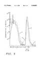
- FIG. 3illustrates in graphical representation the fluorine atom concentration at increasing depths of the polycide gate structure.
- FIG. 1there is illustrated a portion of a partially complete integrated circuit.
- a semiconductor substrate 10preferably composed of monocrystalline silicon.
- Source/drain regions 11are formed as is understood in the art either before or after formation of the gate structure.
- Gate silicon oxide layer 12is deposited over the surface of the substrate 10. Typically, the gate oxide thickness between about 40 to 400 Angstroms.
- the gate polysilicon layer 14is deposited over the gate oxide layer. The thickness of the polysilicon layer is between about 800 to 4000 Angstroms.
- a layer of tungsten silicide 18is deposited by low pressure chemical vapor deposition (LPCVD) to a thickness of between about 800 to 4000 Angstroms.
- LPCVDlow pressure chemical vapor deposition
- the layers 14 and 18are patterned to form the desired polycide gate electrodes.
- the source/drain regions 11are formed by ion implantation of, for example N+ impurities, such as phosphorus or arsenic ions. After the source/drain regions and gate electrode patterns have been defined, the wafer is annealed.
- WF 6 and SiH 4are the main reaction gases in the deposition of tungsten silicide layer 18.
- a large number of fluorine atomsare incorporated into the tungsten silicide layer.
- fluorine atomsdiffuse from the tungsten silicide through the polysilicon 14 to the gate oxide 12.
- the fluorine atomsreact with the oxide and break the Si-O bonds by replacing oxygen at those sites.
- the released oxygendiffuses to the interface and oxidizes the sillcon and polysilicon resulting in additional oxide thickness 20.
- Gate oxide layer 12is deposited on the surface of the monocrystalline semiconductor substrate 10.
- the gate oxide thicknessis between about 40 to 400 Angstroms.
- the gate polysilicon layer 14is deposited over the gate oxide layer, The thickness of the polysilicon layer is between about 800 to 4000 Angstroms.
- a thin conducting diffusion barrier layer 16is introduced between the polysilicon and tungsten silicide layers to minimize the diffusion of fluorine atoms from the tungsten silicide to the gate oxide layer.
- Reactive sputtered titanium nitrideTiN x
- TiN xis the preferred barrier material. It has a preferred thickness of between about 150 to 1500 Angstroms.
- N 2is fed into the sputter chamber with a titanium target. The sputtered titanium atoms react with the N 2 to form TiN x on the silicon wafer.
- Other conductive barrier layers for the diffusion barrier layerare titanium tungsten (TiW) or tantalum nitride (TAN) which are sputtered in the similar way as the titanium nitride.
- tungsten silicide 18is deposited by low pressure chemical vapor deposition (LPCVD) to a thickness of between about 800 to 4000 Angstroms.
- LPCVDlow pressure chemical vapor deposition
- the layers 14, 16, and 18are patterned to form the desired polycide gate electrodes.
- the source/drain regions 11are formed by ion implantation of, for example N+ impurities, such as phosphorus or arsenic ions.
- the waferis annealed, normally at a temperature of between about 800° to 1050° C. in the ambient of N 2 and O 2 for about 10 to 60 minutes.
- the barrier diffusion layer 16minimizes the diffusion of fluorine atoms from the tungsten silicide layer into the polysilicon and gate oxide layers.
- the gate silicon oxide thicknessis not increased after annealing as in the prior art. Low resistance and low stress are maintained and high temperature stability is achieved by the process of the present invention along with no degradation of the device.
- Table Ishows the gate structure and resulting gate oxide thickness for example 1, as deposited, and for examples 2, 3, and 4 after annealing at 1000° C. for 40 minutes in an oxygen atmosphere of 10 standard liters per minute.
- Example 1shows the as-deposited thicknesses of the polycide gate structure and the gate oxide.
- Example 2used the conventional process of the prior art. After annealing, the gate oxide thickness had increased by 10 Angstroms. (Note that transmission electron microscopy (TEM) was used to measure thicknesses. There is an error of +/-3 Angstroms).
- Examples 3 and 4used the process of the invention wherein a diffusion barrier of titanium nitride was used with a thickness of 600 Angstroms. Where a rapid thermal process (RTP) was used for the TiNx layer, the gate oxide thickness was unchanged from the as-deposited thickness in Example 1.
- RTPrapid thermal process
- FIG. 3there is shown the SIMS analysis of the fluorine concentration in atoms per cubic centimeter at increasing depths of the gate electrode structure for the three examples 2, 3, and 4 from Table I above.
- the layers of the gate structureare identified on the x-axis of the graph. It can be seen that the highest and most broad fluorine peak in the gate oxide was observed in example 2, as shown by solid line 2. No local fluorine peak was observed at the interface of the tungsten silicide iWSi x ) and the polysilicon layers for example 2.
- the fluorine concentration in the gate oxideis lowest for example 4 shown by dashed line 4.
- Example 3is illustrated by the dotted line 3.
Landscapes
- Engineering & Computer Science (AREA)
- Chemical & Material Sciences (AREA)
- Chemical Kinetics & Catalysis (AREA)
- Physics & Mathematics (AREA)
- Condensed Matter Physics & Semiconductors (AREA)
- General Physics & Mathematics (AREA)
- Manufacturing & Machinery (AREA)
- Computer Hardware Design (AREA)
- Microelectronics & Electronic Packaging (AREA)
- Power Engineering (AREA)
- Insulated Gate Type Field-Effect Transistor (AREA)
- Electrodes Of Semiconductors (AREA)
Abstract
Description
1. Field of the Invention
The invention relates to a method of fabricating a polycide gate structure, and more particularly, to a method of fabricating a polycide gate structure while preventing fluorine-induced gate oxide degradation in the manufacture of integrated circuits.
2. Description of the Prior Art
Low pressure chemical vapor deposited (LPCVD) tungsten silicide (WSix) has been widely used in the polycide gate structure. WFe and SiH4 are the main reaction gases. A large number of fluorine atoms are incorporated into the tungsten silicide layer during the deposition process. The paper, "Direct Evidence of Gate Oxide Thickness Increase In Tungsten Polycide Processes" by S. L. Hsu et al, IEEE Electron Device Letters, Vol. 12, No. 11, November 1991, pp. 623-625, shows that the fluorine atoms "diffused from tungsten silicide films to gate oxides causes additional growth." This additional gate oxide will cause device degradation such as a shift in threshold voltage and a descrease in saturation current.
A principal object of the present invention is to provide an effective and very manufacturable method of preventing fluorine-induced gate oxide degradation in The fabrication of a polycide gate structure.
In accordance with the object of this invention a new method of fabricating a polycide gate structure is achieved. A gate polysilicon layer is provided overlying a gate oxide layer on the surface of a semiconductor substrate. A thin conducting diffusion barrier layer is deposited overlying the gate polysilicon layer, A layer of tungsten silicide is deposited overlying the thin conducting diffusion barrier layer wherein a reaction gas used in the deposition contains fluorine atoms and wherein the fluorine atoms are incorporated into the tungsten silicide layer. The gate polysilicon, thin conducting diffusion barrier, and tungsten silicide layers are patterned to form the polycide gate structures. The wafer is annealed to complete formation of the polycide gate structures wherein the number of fluorine atoms from the tungsten silicide layer diffusing into the gate polysilicon layer are minimized by the presence of the thin conducting diffusion barrier layer and wherein because the diffusion of the fluorine atoms is minimized, the thickness of the gate oxide layer does not increase. This prevents the device from degradation such as threshold voltage shift and saturation current descrease.
In the accompanying drawings forming a material part of this description, there is shown:
FIG. 1 schematically illustrates in cross-sectional representation an embodiment of the prior art.
FIG. 2 schematically illustrates in cross-sectional representation one preferred embodiment of the present invention.
FIG. 3 illustrates in graphical representation the fluorine atom concentration at increasing depths of the polycide gate structure.
Referring now more particularly to FIG. 1, there is illustrated a portion of a partially complete integrated circuit. There is shown asemiconductor substrate 10, preferably composed of monocrystalline silicon. Source/drain regions 11 are formed as is understood in the art either before or after formation of the gate structure. Gatesilicon oxide layer 12 is deposited over the surface of thesubstrate 10. Typically, the gate oxide thickness between about 40 to 400 Angstroms. Next, thegate polysilicon layer 14 is deposited over the gate oxide layer. The thickness of the polysilicon layer is between about 800 to 4000 Angstroms.
To complete the polycide gate structure, a layer oftungsten silicide 18 is deposited by low pressure chemical vapor deposition (LPCVD) to a thickness of between about 800 to 4000 Angstroms. Using conventional photolithography and etching techniques, thelayers drain regions 11 are formed by ion implantation of, for example N+ impurities, such as phosphorus or arsenic ions. After the source/drain regions and gate electrode patterns have been defined, the wafer is annealed.
WF6 and SiH4 are the main reaction gases in the deposition oftungsten silicide layer 18. A large number of fluorine atoms are incorporated into the tungsten silicide layer. When the polycide structure is annealed at high temperatures, fluorine atoms diffuse from the tungsten silicide through thepolysilicon 14 to thegate oxide 12. The fluorine atoms react with the oxide and break the Si-O bonds by replacing oxygen at those sites. The released oxygen diffuses to the interface and oxidizes the sillcon and polysilicon resulting inadditional oxide thickness 20.
Referring now to FIG. 2, the process of the present invention will be described. Processing begins as described above in the prior art process.Gate oxide layer 12 is deposited on the surface of themonocrystalline semiconductor substrate 10. The gate oxide thickness is between about 40 to 400 Angstroms. Next, thegate polysilicon layer 14 is deposited over the gate oxide layer, The thickness of the polysilicon layer is between about 800 to 4000 Angstroms.
A thin conductingdiffusion barrier layer 16 is introduced between the polysilicon and tungsten silicide layers to minimize the diffusion of fluorine atoms from the tungsten silicide to the gate oxide layer. Reactive sputtered titanium nitride (TiNx) is the preferred barrier material. It has a preferred thickness of between about 150 to 1500 Angstroms. N2 is fed into the sputter chamber with a titanium target. The sputtered titanium atoms react with the N2 to form TiNx on the silicon wafer. Other conductive barrier layers for the diffusion barrier layer are titanium tungsten (TiW) or tantalum nitride (TAN) which are sputtered in the similar way as the titanium nitride.
After deposition of thediffusion barrier layer 16, a layer oftungsten silicide 18 is deposited by low pressure chemical vapor deposition (LPCVD) to a thickness of between about 800 to 4000 Angstroms. Using conventional photolithography and etching techniques, thelayers drain regions 11 are formed by ion implantation of, for example N+ impurities, such as phosphorus or arsenic ions. The wafer is annealed, normally at a temperature of between about 800° to 1050° C. in the ambient of N2 and O2 for about 10 to 60 minutes.
Thebarrier diffusion layer 16 minimizes the diffusion of fluorine atoms from the tungsten silicide layer into the polysilicon and gate oxide layers. The gate silicon oxide thickness is not increased after annealing as in the prior art. Low resistance and low stress are maintained and high temperature stability is achieved by the process of the present invention along with no degradation of the device.
The integrated circuit is completed as is conventional in the art.
The following Examples are given to show the important features of the invention and to aid in the understanding thereof and variations may be made by one skilled in the art without departing from the spirit and scope of the invention.
Table I shows the gate structure and resulting gate oxide thickness for example 1, as deposited, and for examples 2, 3, and 4 after annealing at 1000° C. for 40 minutes in an oxygen atmosphere of 10 standard liters per minute.
TABLE I ______________________________________ structure RTP of TiNx gate oxide EXAMPLE WSix/TiNx/Poly-Si 750° C., 20 sec thickness ______________________________________ 1 2000/0/2000 A -- 212A 2 2000/0/2000 A -- 222A 3 1400/600/2000 A No 217A 4 1400/600/2000 A Yes 212 A ______________________________________
Example 1 shows the as-deposited thicknesses of the polycide gate structure and the gate oxide. Example 2 used the conventional process of the prior art. After annealing, the gate oxide thickness had increased by 10 Angstroms. (Note that transmission electron microscopy (TEM) was used to measure thicknesses. There is an error of +/-3 Angstroms). Examples 3 and 4 used the process of the invention wherein a diffusion barrier of titanium nitride was used with a thickness of 600 Angstroms. Where a rapid thermal process (RTP) was used for the TiNx layer, the gate oxide thickness was unchanged from the as-deposited thickness in Example 1.
Referring now to FIG. 3, there is shown the SIMS analysis of the fluorine concentration in atoms per cubic centimeter at increasing depths of the gate electrode structure for the three examples 2, 3, and 4 from Table I above. The layers of the gate structure are identified on the x-axis of the graph. It can be seen that the highest and most broad fluorine peak in the gate oxide was observed in example 2, as shown bysolid line 2. No local fluorine peak was observed at the interface of the tungsten silicide iWSix) and the polysilicon layers for example 2. The fluorine concentration in the gate oxide is lowest for example 4 shown by dashedline 4. Example 3 is illustrated by the dottedline 3.
While the invention has been particularly shown and described with reference to the preferred embodiments thereof it will be understood by those skilled in the art that various changes in form and details may be made without departing from the spirit and scope of the invention.
Claims (9)
1. The method of fabricating polycide gate structures without fluorine-induced degradation of the gate silicon oxide layer comprising:
providing a gate polysilicon layer overlying said gate silicon oxide layer on the surface of a semiconductor substrate;
depositing a thin conducting diffusion barrier layer having a thickness of between about 150 to 1500 Angstroms overlying said gate polysilicon layer;
depositing a layer of tungsten silicide overlying said thin conducting diffusion barrier layer wherein a reaction gas used in said depositing of tungsten silicide contains fluorine atoms and wherein said fluorine atoms are incorporated into said layer of tungsten silicide;
patterning said gate polysilicon, thin conducting diffusion barrier, and tungsten silicide layers to form said polycide gate structures; and
annealing said substrate at a temperature of between about 800° to 1050° C. for between about 10 to 60 minutes to complete formation of said polycide gate structures wherein the number of said fluorine atoms from said tungsten silicide layer diffusing into said gate polysilicon layer are minimized by the presence of said thin conducting diffusion barrier layer and thereby said gate silicon oxide layer thickness is not increased.
2. The method of claim 1 wherein said thin conducting diffusion barrier layer is composed of titanium nitride.
3. The method of claim 1 wherein said thin conducting diffusion barrier layer is composed of tantalum nitride.
4. The method of claim 1 wherein said thin conducting diffusion barrier layer is composed of titanium/tungsten.
5. The method of fabricating polycide gate structures comprising:
providing a gate polysilicon layer overlying a gate silicon oxide layer on the surface of a semiconductor substrate;
depositing a thin conducting diffusion barrier layer having a thickness of between about 150 to 1500 Angstroms overlying said gate polysilicon layer;
depositing a layer of tungsten silicide using a fluoride based deposition process overlying said thin conducting diffusion barrier layer;
patterning said gate polysilicon, thin conducting diffusion barrier, and tungsten silicide layers to form said polycide gate structures; and
annealing said substrate at a temperature of between about 800° to 1050° C. for between about 10 to 60 minutes to complete formation of said polycide gate structures.
6. The method of claim 5, wherein said thin conducting diffusion barrier layer is composed of titanium nitride.
7. The method of claim 5 wherein a fluorine-containing reaction gas used in said deposition of said tungsten silicide layer contains fluorine atoms which are incorporated into said tungsten silicide layer and wherein the number of said fluorine atoms from said tungsten silicide layer diffusing into said gate polysilicon layer are minimized by the presence of said thin conducting diffusion barrier layer and wherein because said diffusion of said fluorine atoms is minimized, said gate oxide layer thickness is not increased.
8. The method of claim 5 wherein said thin conducting diffusion barrier layer is composed of tantalum nitride.
9. The method of claim 5 wherein said thin conducting diffusion barrier layer is composed of titanium/tungsten.
Priority Applications (2)
| Application Number | Priority Date | Filing Date | Title |
|---|---|---|---|
| US08/080,304US5364803A (en) | 1993-06-24 | 1993-06-24 | Method of preventing fluorine-induced gate oxide degradation in WSix polycide structure |
| US08/582,599US5668394A (en) | 1993-06-24 | 1996-01-03 | Prevention of fluorine-induced gate oxide degradation in WSi polycide structure |
Applications Claiming Priority (1)
| Application Number | Priority Date | Filing Date | Title |
|---|---|---|---|
| US08/080,304US5364803A (en) | 1993-06-24 | 1993-06-24 | Method of preventing fluorine-induced gate oxide degradation in WSix polycide structure |
Related Child Applications (1)
| Application Number | Title | Priority Date | Filing Date |
|---|---|---|---|
| US33639794ADivision | 1993-06-24 | 1994-11-09 |
Publications (1)
| Publication Number | Publication Date |
|---|---|
| US5364803Atrue US5364803A (en) | 1994-11-15 |
Family
ID=22156531
Family Applications (2)
| Application Number | Title | Priority Date | Filing Date |
|---|---|---|---|
| US08/080,304Expired - LifetimeUS5364803A (en) | 1993-06-24 | 1993-06-24 | Method of preventing fluorine-induced gate oxide degradation in WSix polycide structure |
| US08/582,599Expired - LifetimeUS5668394A (en) | 1993-06-24 | 1996-01-03 | Prevention of fluorine-induced gate oxide degradation in WSi polycide structure |
Family Applications After (1)
| Application Number | Title | Priority Date | Filing Date |
|---|---|---|---|
| US08/582,599Expired - LifetimeUS5668394A (en) | 1993-06-24 | 1996-01-03 | Prevention of fluorine-induced gate oxide degradation in WSi polycide structure |
Country Status (1)
| Country | Link |
|---|---|
| US (2) | US5364803A (en) |
Cited By (49)
| Publication number | Priority date | Publication date | Assignee | Title |
|---|---|---|---|---|
| US5518958A (en)* | 1994-07-29 | 1996-05-21 | International Business Machines Corporation | Prevention of agglomeration and inversion in a semiconductor polycide process |
| US5527718A (en)* | 1993-12-28 | 1996-06-18 | Sony Corporation | Process for removing impurities from polycide electrode and insulating film using heat |
| US5559047A (en)* | 1994-06-29 | 1996-09-24 | Nec Corporation | Method of reliably manufacturing a semiconductor device having a titanium silicide nitride |
| US5614428A (en)* | 1995-10-23 | 1997-03-25 | Lsi Logic Corporation | Process and structure for reduction of channeling during implantation of source and drain regions in formation of MOS integrated circuit structures |
| US5652156A (en)* | 1995-04-10 | 1997-07-29 | Taiwan Semiconductor Manufacturing Company Ltd. | Layered polysilicon deposition method |
| US5712181A (en)* | 1993-07-20 | 1998-01-27 | Lg Semicon Co., Ltd. | Method for the formation of polycide gate in semiconductor device |
| US5712208A (en)* | 1994-06-09 | 1998-01-27 | Motorola, Inc. | Methods of formation of semiconductor composite gate dielectric having multiple incorporated atomic dopants |
| US5726096A (en)* | 1993-12-17 | 1998-03-10 | Hyundai Electronics Industries Co., Ltd. | Method for forming a tungsten silicide layer in a semiconductor device |
| US5733816A (en)* | 1995-12-13 | 1998-03-31 | Micron Technology, Inc. | Method for depositing a tungsten layer on silicon |
| US5736455A (en)* | 1995-12-22 | 1998-04-07 | Micron Technology, Inc. | Method for passivating the sidewalls of a tungsten word line |
| US5756392A (en)* | 1997-01-22 | 1998-05-26 | Taiwan Semiconductor Manuacturing Company, Ltd. | Method of formation of polycide in a semiconductor IC device |
| US5767558A (en)* | 1996-05-10 | 1998-06-16 | Integrated Device Technology, Inc. | Structures for preventing gate oxide degradation |
| US5776823A (en)* | 1995-01-12 | 1998-07-07 | Ibm Corporation | Tasin oxygen diffusion barrier in multilayer structures |
| US5795817A (en)* | 1995-03-30 | 1998-08-18 | Samsung Electronics Co., Ltd. | MOS transistor adopting titanium-carbon-nitride gate electrode and manufacturing method thereof |
| US5798296A (en)* | 1996-05-17 | 1998-08-25 | Micron Technology, Inc. | Method of fabricating a gate having a barrier of titanium silicide |
| US5804488A (en)* | 1995-08-24 | 1998-09-08 | Taiwan Semiconductor Manufacturing Company, Ltd. | Method of forming a tungsten silicide capacitor having a high breakdown voltage |
| US5830802A (en)* | 1995-08-31 | 1998-11-03 | Motorola Inc. | Process for reducing halogen concentration in a material layer during semiconductor device fabrication |
| US5888588A (en)* | 1997-03-31 | 1999-03-30 | Motorola, Inc. | Process for forming a semiconductor device |
| US5923999A (en)* | 1996-10-29 | 1999-07-13 | International Business Machines Corporation | Method of controlling dopant diffusion and metal contamination in thin polycide gate conductor of mosfet device |
| US5946599A (en)* | 1997-07-24 | 1999-08-31 | Taiwan Semiconductor Manufacturing Company, Ltd. | Method of manufacturing a semiconductor IC device |
| US5958508A (en)* | 1997-03-31 | 1999-09-28 | Motorlola, Inc. | Process for forming a semiconductor device |
| US6001718A (en)* | 1997-09-30 | 1999-12-14 | Kabushiki Kaisha Toshiba | Semiconductor device having a ternary compound low resistive electrode |
| US6001675A (en)* | 1996-01-31 | 1999-12-14 | Micron Technology, Inc. | Method of forming a thin film transistor |
| US6043138A (en)* | 1996-09-16 | 2000-03-28 | Advanced Micro Devices, Inc. | Multi-step polysilicon deposition process for boron penetration inhibition |
| US6084279A (en)* | 1997-03-31 | 2000-07-04 | Motorola Inc. | Semiconductor device having a metal containing layer overlying a gate dielectric |
| US6087214A (en)* | 1998-04-29 | 2000-07-11 | Vlsi Technology, Inc. | Arrangement and method for DRAM cell using shallow trench isolation |
| US6100171A (en)* | 1998-03-03 | 2000-08-08 | Advanced Micro Devices, Inc. | Reduction of boron penetration by laser anneal removal of fluorine |
| US6143618A (en)* | 1998-09-18 | 2000-11-07 | Taiwan Semiconductor Manufacturing Company | Procedure for elimating flourine degradation of WSix /oxide/polysilicon capacitors |
| US6146742A (en)* | 1997-11-24 | 2000-11-14 | United Microelectronics Corp. | Barrier/glue layer on polysilicon layer |
| US6153519A (en)* | 1997-03-31 | 2000-11-28 | Motorola, Inc. | Method of forming a barrier layer |
| US6165884A (en)* | 1998-12-22 | 2000-12-26 | Hyundai Electronics Industries Co., Ltd. | Method of forming gate electrode in semiconductor device |
| KR20010008442A (en)* | 1998-12-31 | 2001-02-05 | 김영환 | Transistor Formation Method of Semiconductor Device |
| US6187664B1 (en) | 1995-06-05 | 2001-02-13 | Taiwan Semiconductor Manufacturing Company | Method for forming a barrier metallization layer |
| US6294435B1 (en) | 1999-10-08 | 2001-09-25 | Vanguard International Semiconductor Corporation | Method of reducing word line resistance and contact resistance |
| US6329670B1 (en) | 1999-04-06 | 2001-12-11 | Micron Technology, Inc. | Conductive material for integrated circuit fabrication |
| CN1076865C (en)* | 1995-04-28 | 2001-12-26 | 现代电子产业株式会社 | Method of forming two-layered polysilicon gate electrode in semiconductor device using grain boundaries |
| US6373114B1 (en)* | 1998-10-23 | 2002-04-16 | Micron Technology, Inc. | Barrier in gate stack for improved gate dielectric integrity |
| US6420275B1 (en) | 1999-08-30 | 2002-07-16 | Micron Technology, Inc. | System and method for analyzing a semiconductor surface |
| US6423632B1 (en)* | 2000-07-21 | 2002-07-23 | Motorola, Inc. | Semiconductor device and a process for forming the same |
| KR100332124B1 (en)* | 1995-03-07 | 2002-09-04 | 주식회사 하이닉스반도체 | Method for forming gate electrode in semiconductor device |
| US6511900B2 (en) | 1999-08-24 | 2003-01-28 | Micron Technology, Inc. | Boron incorporated diffusion barrier material |
| US6514818B1 (en)* | 1997-12-12 | 2003-02-04 | Hyundai Electronics Industries Co., Ltd. | Nonvolatile ferroelectric memory without a separate cell plate line and method of manufacturing the same |
| DE19652070C2 (en)* | 1995-12-15 | 2003-02-20 | Hyundai Electronics Ind | Gate electrode and method of making the same |
| US6611032B2 (en) | 1999-06-15 | 2003-08-26 | Micron Technology, Inc. | Methods for forming wordlines, transistor gates, and conductive interconnects, and wordline, transistor gate, and conductive interconnect structures |
| US6613654B1 (en) | 1999-01-29 | 2003-09-02 | Micron Technology Inc | Fabrication of semiconductor devices with transition metal boride films as diffusion barriers |
| US20030189253A1 (en)* | 1999-06-11 | 2003-10-09 | Schuegraf Klaus Florian | Methods for forming wordlines, transistor gates, and conductive interonnects, and wordline, transistor gate, and conductive interconnect structures |
| KR100800647B1 (en)* | 2006-08-29 | 2008-02-01 | 동부일렉트로닉스 주식회사 | Gate electrode formation method of semiconductor device |
| US9960118B2 (en) | 2016-01-20 | 2018-05-01 | Globalfoundries Inc. | Contact using multilayer liner |
| US20180374922A1 (en)* | 2017-06-22 | 2018-12-27 | United Microelectronics Corp. | Semiconductor structure and manufacturing method thereof |
Families Citing this family (23)
| Publication number | Priority date | Publication date | Assignee | Title |
|---|---|---|---|---|
| KR0179677B1 (en)* | 1993-12-28 | 1999-04-15 | 사토 후미오 | Semiconductor device wiring or electrode |
| KR100207472B1 (en) | 1996-06-07 | 1999-07-15 | 윤종용 | Semiconductor device for gate electrode having & manufacturing method of the same |
| KR100325383B1 (en)* | 1996-07-12 | 2002-04-17 | 니시무로 타이죠 | Semiconductor device and method of manufacturing the same |
| US6080645A (en) | 1996-10-29 | 2000-06-27 | Micron Technology, Inc. | Method of making a doped silicon diffusion barrier region |
| US6015997A (en)* | 1997-02-19 | 2000-01-18 | Micron Technology, Inc. | Semiconductor structure having a doped conductive layer |
| US6262458B1 (en) | 1997-02-19 | 2001-07-17 | Micron Technology, Inc. | Low resistivity titanium silicide structures |
| US5926730A (en) | 1997-02-19 | 1999-07-20 | Micron Technology, Inc. | Conductor layer nitridation |
| US5925918A (en)* | 1997-07-30 | 1999-07-20 | Micron, Technology, Inc. | Gate stack with improved sidewall integrity |
| US7009264B1 (en) | 1997-07-30 | 2006-03-07 | Micron Technology, Inc. | Selective spacer to prevent metal oxide formation during polycide reoxidation |
| KR100425147B1 (en)* | 1997-09-29 | 2004-05-17 | 주식회사 하이닉스반도체 | Method for manufacturing semiconductor device |
| KR100475897B1 (en)* | 1997-12-29 | 2005-06-21 | 주식회사 하이닉스반도체 | Manufacturing method of semiconductor device |
| US6110788A (en) | 1998-09-16 | 2000-08-29 | Micron Technology, Inc. | Surface channel MOS transistors, methods for making the same, and semiconductor devices containing the same |
| US6060741A (en)* | 1998-09-16 | 2000-05-09 | Advanced Micro Devices, Inc. | Stacked gate structure for flash memory application |
| KR100318459B1 (en) | 1998-12-22 | 2002-02-19 | 박종섭 | A method for forming titanium polycide gate electrode |
| KR20000042876A (en) | 1998-12-28 | 2000-07-15 | 김영환 | Method for forming gate electrode of semiconductor device |
| JP3988342B2 (en) | 1998-12-29 | 2007-10-10 | 株式会社ハイニックスセミコンダクター | Method for forming gate electrode of semiconductor element |
| EP1205980A1 (en)* | 2000-11-07 | 2002-05-15 | Infineon Technologies AG | A method for forming a field effect transistor in a semiconductor substrate |
| US6537909B1 (en)* | 2002-01-03 | 2003-03-25 | United Microelectronics Corp. | Method of preventing silicide spiking |
| KR100654002B1 (en)* | 2005-11-22 | 2006-12-06 | 주식회사 하이닉스반도체 | Method for manufacturing semiconductor device having tungsten-polyside gate and recess channel |
| KR100654001B1 (en) | 2005-11-22 | 2006-12-06 | 주식회사 하이닉스반도체 | Method of manufacturing semiconductor device having recess channel |
| US7510956B2 (en)* | 2006-01-30 | 2009-03-31 | Fressscale Semiconductor, Inc. | MOS device with multi-layer gate stack |
| US8432000B2 (en) | 2010-06-18 | 2013-04-30 | Fairchild Semiconductor Corporation | Trench MOS barrier schottky rectifier with a planar surface using CMP techniques |
| US20210126103A1 (en)* | 2019-10-29 | 2021-04-29 | Micron Technology, Inc. | Apparatus comprising wordlines comprising multiple metal materials, and related methods and electronic systems |
Citations (2)
| Publication number | Priority date | Publication date | Assignee | Title |
|---|---|---|---|---|
| US4640004A (en)* | 1984-04-13 | 1987-02-03 | Fairchild Camera & Instrument Corp. | Method and structure for inhibiting dopant out-diffusion |
| US4962414A (en)* | 1988-02-11 | 1990-10-09 | Sgs-Thomson Microelectronics, Inc. | Method for forming a contact VIA |
Family Cites Families (5)
| Publication number | Priority date | Publication date | Assignee | Title |
|---|---|---|---|---|
| EP0077813B1 (en)* | 1981-05-04 | 1986-02-05 | Motorola, Inc. | Low resistivity composite metallization for semiconductor devices and method therefor |
| JPS6213075A (en)* | 1985-07-10 | 1987-01-21 | Nec Corp | Semiconductor device |
| US4782380A (en)* | 1987-01-22 | 1988-11-01 | Advanced Micro Devices, Inc. | Multilayer interconnection for integrated circuit structure having two or more conductive metal layers |
| JPH02155273A (en)* | 1988-12-07 | 1990-06-14 | Nec Corp | Mos field-effect transistor |
| JPH0350770A (en)* | 1989-07-18 | 1991-03-05 | Seiko Epson Corp | MOS type semiconductor integrated circuit device |
- 1993
- 1993-06-24USUS08/080,304patent/US5364803A/ennot_activeExpired - Lifetime
- 1996
- 1996-01-03USUS08/582,599patent/US5668394A/ennot_activeExpired - Lifetime
Patent Citations (2)
| Publication number | Priority date | Publication date | Assignee | Title |
|---|---|---|---|---|
| US4640004A (en)* | 1984-04-13 | 1987-02-03 | Fairchild Camera & Instrument Corp. | Method and structure for inhibiting dopant out-diffusion |
| US4962414A (en)* | 1988-02-11 | 1990-10-09 | Sgs-Thomson Microelectronics, Inc. | Method for forming a contact VIA |
Non-Patent Citations (2)
| Title |
|---|
| Hsu et al., "Direct Evidence of Gate Oxide Thickness Increase in Tungsten Polycide Processes", IEEE Elec. Dev. Lett., vol. 12, No. 11, Nov. 1991, pp. 623-625. |
| Hsu et al., Direct Evidence of Gate Oxide Thickness Increase in Tungsten Polycide Processes , IEEE Elec. Dev. Lett., vol. 12, No. 11, Nov. 1991, pp. 623 625.* |
Cited By (116)
| Publication number | Priority date | Publication date | Assignee | Title |
|---|---|---|---|---|
| US5712181A (en)* | 1993-07-20 | 1998-01-27 | Lg Semicon Co., Ltd. | Method for the formation of polycide gate in semiconductor device |
| US5726096A (en)* | 1993-12-17 | 1998-03-10 | Hyundai Electronics Industries Co., Ltd. | Method for forming a tungsten silicide layer in a semiconductor device |
| US5527718A (en)* | 1993-12-28 | 1996-06-18 | Sony Corporation | Process for removing impurities from polycide electrode and insulating film using heat |
| US5712208A (en)* | 1994-06-09 | 1998-01-27 | Motorola, Inc. | Methods of formation of semiconductor composite gate dielectric having multiple incorporated atomic dopants |
| US5559047A (en)* | 1994-06-29 | 1996-09-24 | Nec Corporation | Method of reliably manufacturing a semiconductor device having a titanium silicide nitride |
| US5518958A (en)* | 1994-07-29 | 1996-05-21 | International Business Machines Corporation | Prevention of agglomeration and inversion in a semiconductor polycide process |
| US5776823A (en)* | 1995-01-12 | 1998-07-07 | Ibm Corporation | Tasin oxygen diffusion barrier in multilayer structures |
| KR100332124B1 (en)* | 1995-03-07 | 2002-09-04 | 주식회사 하이닉스반도체 | Method for forming gate electrode in semiconductor device |
| US5965911A (en)* | 1995-03-30 | 1999-10-12 | Samsung Electronics Co., Ltd. | Mos transistor adopting titanium-carbon-nitride gate electrode and manufacturing method thereof |
| US5795817A (en)* | 1995-03-30 | 1998-08-18 | Samsung Electronics Co., Ltd. | MOS transistor adopting titanium-carbon-nitride gate electrode and manufacturing method thereof |
| US5652156A (en)* | 1995-04-10 | 1997-07-29 | Taiwan Semiconductor Manufacturing Company Ltd. | Layered polysilicon deposition method |
| CN1076865C (en)* | 1995-04-28 | 2001-12-26 | 现代电子产业株式会社 | Method of forming two-layered polysilicon gate electrode in semiconductor device using grain boundaries |
| US6187664B1 (en) | 1995-06-05 | 2001-02-13 | Taiwan Semiconductor Manufacturing Company | Method for forming a barrier metallization layer |
| US5804488A (en)* | 1995-08-24 | 1998-09-08 | Taiwan Semiconductor Manufacturing Company, Ltd. | Method of forming a tungsten silicide capacitor having a high breakdown voltage |
| US5830802A (en)* | 1995-08-31 | 1998-11-03 | Motorola Inc. | Process for reducing halogen concentration in a material layer during semiconductor device fabrication |
| US5614428A (en)* | 1995-10-23 | 1997-03-25 | Lsi Logic Corporation | Process and structure for reduction of channeling during implantation of source and drain regions in formation of MOS integrated circuit structures |
| US5733816A (en)* | 1995-12-13 | 1998-03-31 | Micron Technology, Inc. | Method for depositing a tungsten layer on silicon |
| DE19652070C2 (en)* | 1995-12-15 | 2003-02-20 | Hyundai Electronics Ind | Gate electrode and method of making the same |
| US5736455A (en)* | 1995-12-22 | 1998-04-07 | Micron Technology, Inc. | Method for passivating the sidewalls of a tungsten word line |
| US20090047776A1 (en)* | 1996-01-31 | 2009-02-19 | Micron Technology, Inc. | Method of Forming a Thin Film Transistor |
| US7385222B2 (en)* | 1996-01-31 | 2008-06-10 | Micron Technology, Inc. | Thin film transistors and semiconductor constructions |
| US20050156240A1 (en)* | 1996-01-31 | 2005-07-21 | Sandhu Gurtej S. | Thin film transistors and semiconductor constructions |
| US20070102705A1 (en)* | 1996-01-31 | 2007-05-10 | Sandhu Gurtej S | Thin film transistors and semiconductor constructions |
| US6001675A (en)* | 1996-01-31 | 1999-12-14 | Micron Technology, Inc. | Method of forming a thin film transistor |
| US20080237601A1 (en)* | 1996-01-31 | 2008-10-02 | Sandhu Gurtej S | Transistors and semiconductor constructions |
| US7452760B2 (en) | 1996-01-31 | 2008-11-18 | Micron Technology, Inc. | Thin film transistors and semiconductor constructions |
| US6344376B2 (en) | 1996-01-31 | 2002-02-05 | Micron Technology, Inc. | Method of forming a thin film transistor |
| US6890842B2 (en)* | 1996-01-31 | 2005-05-10 | Micron Technology, Inc. | Method of forming a thin film transistor |
| US20010044173A1 (en)* | 1996-01-31 | 2001-11-22 | Sandhu Gurtej S. | Method of forming a thin film transistor |
| US7566907B2 (en) | 1996-01-31 | 2009-07-28 | Micron Technology, Inc. | Thin film transistors and semiconductor constructions |
| US6238957B1 (en) | 1996-01-31 | 2001-05-29 | Micron Technology, Inc. | Method of forming a thin film transistor |
| US20090302322A1 (en)* | 1996-01-31 | 2009-12-10 | Micron Technology, Inc. | Method of Forming a Thin Film Transistor |
| US7825414B2 (en) | 1996-01-31 | 2010-11-02 | Micron Technology, Inc. | Method of forming a thin film transistor |
| US6093589A (en)* | 1996-05-10 | 2000-07-25 | Integrated Device Technology, Inc. | Methods for preventing gate oxide degradation |
| US5767558A (en)* | 1996-05-10 | 1998-06-16 | Integrated Device Technology, Inc. | Structures for preventing gate oxide degradation |
| US5798296A (en)* | 1996-05-17 | 1998-08-25 | Micron Technology, Inc. | Method of fabricating a gate having a barrier of titanium silicide |
| US6087700A (en)* | 1996-05-17 | 2000-07-11 | Micron Technology, Inc. | Gate having a barrier of titanium silicide |
| US6107176A (en)* | 1996-05-17 | 2000-08-22 | Micron Technology, Inc. | Method of fabricating a gate having a barrier of titanium silicide |
| US6043138A (en)* | 1996-09-16 | 2000-03-28 | Advanced Micro Devices, Inc. | Multi-step polysilicon deposition process for boron penetration inhibition |
| US5923999A (en)* | 1996-10-29 | 1999-07-13 | International Business Machines Corporation | Method of controlling dopant diffusion and metal contamination in thin polycide gate conductor of mosfet device |
| US6114736A (en)* | 1996-10-29 | 2000-09-05 | International Business Machines Corporation | Controlled dopant diffusion and metal contamination in thin polycide gate conductor of MOSFET device |
| US5756392A (en)* | 1997-01-22 | 1998-05-26 | Taiwan Semiconductor Manuacturing Company, Ltd. | Method of formation of polycide in a semiconductor IC device |
| US5888588A (en)* | 1997-03-31 | 1999-03-30 | Motorola, Inc. | Process for forming a semiconductor device |
| US6084279A (en)* | 1997-03-31 | 2000-07-04 | Motorola Inc. | Semiconductor device having a metal containing layer overlying a gate dielectric |
| US6376371B1 (en) | 1997-03-31 | 2002-04-23 | Motorola, Inc. | Method of forming a semiconductor device |
| US5958508A (en)* | 1997-03-31 | 1999-09-28 | Motorlola, Inc. | Process for forming a semiconductor device |
| US6153519A (en)* | 1997-03-31 | 2000-11-28 | Motorola, Inc. | Method of forming a barrier layer |
| US5946599A (en)* | 1997-07-24 | 1999-08-31 | Taiwan Semiconductor Manufacturing Company, Ltd. | Method of manufacturing a semiconductor IC device |
| US6001718A (en)* | 1997-09-30 | 1999-12-14 | Kabushiki Kaisha Toshiba | Semiconductor device having a ternary compound low resistive electrode |
| US6146742A (en)* | 1997-11-24 | 2000-11-14 | United Microelectronics Corp. | Barrier/glue layer on polysilicon layer |
| US7053434B2 (en) | 1997-12-12 | 2006-05-30 | Hyundai Electronics Industries Co., Ltd. | Ferroelectric memory device and method of making the same |
| US6514818B1 (en)* | 1997-12-12 | 2003-02-04 | Hyundai Electronics Industries Co., Ltd. | Nonvolatile ferroelectric memory without a separate cell plate line and method of manufacturing the same |
| US20060028892A1 (en)* | 1997-12-12 | 2006-02-09 | Hyundai Electronics Industries Co., Ltd. | Ferroelectric memory device and method of making the same |
| US20030087480A1 (en)* | 1997-12-12 | 2003-05-08 | Hyundai Electronics Industries Co., Ltd. | Ferroelectric memory device and method of making the same |
| US20050265067A1 (en)* | 1997-12-12 | 2005-12-01 | Hyundai Electronics Industries Co., Ltd. | Ferroelectric memory device and method of making the same |
| US6949441B2 (en) | 1997-12-12 | 2005-09-27 | Hyundai Electronics Industries Co., Ltd. | Ferroelectric memory device and method of making the same |
| US6100171A (en)* | 1998-03-03 | 2000-08-08 | Advanced Micro Devices, Inc. | Reduction of boron penetration by laser anneal removal of fluorine |
| US6087214A (en)* | 1998-04-29 | 2000-07-11 | Vlsi Technology, Inc. | Arrangement and method for DRAM cell using shallow trench isolation |
| US6143618A (en)* | 1998-09-18 | 2000-11-07 | Taiwan Semiconductor Manufacturing Company | Procedure for elimating flourine degradation of WSix /oxide/polysilicon capacitors |
| US6930363B2 (en) | 1998-10-23 | 2005-08-16 | Micron Technology, Inc. | Barrier in gate stack for improved gate dielectric integrity |
| US20030139061A1 (en)* | 1998-10-23 | 2003-07-24 | Nanseng Jeng | Barrier in gate stack for improved gate dielectric integrity |
| US20050017312A1 (en)* | 1998-10-23 | 2005-01-27 | Nanseng Jeng | Barrier in gate stack for improved gate dielectric integrity |
| US6562730B2 (en) | 1998-10-23 | 2003-05-13 | Micron Technology, Inc. | Barrier in gate stack for improved gate dielectric integrity |
| US6770571B2 (en) | 1998-10-23 | 2004-08-03 | Micron Technology, Inc. | Barrier in gate stack for improved gate dielectric integrity |
| US6373114B1 (en)* | 1998-10-23 | 2002-04-16 | Micron Technology, Inc. | Barrier in gate stack for improved gate dielectric integrity |
| US6165884A (en)* | 1998-12-22 | 2000-12-26 | Hyundai Electronics Industries Co., Ltd. | Method of forming gate electrode in semiconductor device |
| KR20010008442A (en)* | 1998-12-31 | 2001-02-05 | 김영환 | Transistor Formation Method of Semiconductor Device |
| US6614082B1 (en)* | 1999-01-29 | 2003-09-02 | Micron Technology, Inc. | Fabrication of semiconductor devices with transition metal boride films as diffusion barriers |
| US6613654B1 (en) | 1999-01-29 | 2003-09-02 | Micron Technology Inc | Fabrication of semiconductor devices with transition metal boride films as diffusion barriers |
| US6872639B2 (en) | 1999-01-29 | 2005-03-29 | Micron Technology, Inc. | Fabrication of semiconductor devices with transition metal boride films as diffusion barriers |
| US20030203608A1 (en)* | 1999-01-29 | 2003-10-30 | Deboer Scott J. | Fabrication of semiconductor devices with transition metal boride films as diffusion barriers |
| US6518181B2 (en) | 1999-04-06 | 2003-02-11 | Micron Technology, Inc. | Conductive material for integrated circuit fabrication |
| US20040201398A1 (en)* | 1999-04-06 | 2004-10-14 | Hu Yungjun Jeff | Conductive material for integrated circuit fabrication |
| US6765398B2 (en) | 1999-04-06 | 2004-07-20 | Micron Technology Inc. | Conductive material for integrated circuit fabrication |
| US6329670B1 (en) | 1999-04-06 | 2001-12-11 | Micron Technology, Inc. | Conductive material for integrated circuit fabrication |
| US6781365B2 (en) | 1999-04-06 | 2004-08-24 | Micron Technology, Inc. | Conductive material for integrated circuit fabrication |
| US6699781B2 (en) | 1999-04-06 | 2004-03-02 | Micron Technology Inc. | Conductive material for integrated circuit fabrication |
| US20030183949A1 (en)* | 1999-04-06 | 2003-10-02 | Hu Yungjun Jeff | Conductive material for integrated circuit fabrication |
| US7046029B2 (en) | 1999-04-06 | 2006-05-16 | Micron Technology, Inc. | Conductive material for integrated circuit fabrication |
| US20050225340A1 (en)* | 1999-04-06 | 2005-10-13 | Hu Yungjun J | Conductive material for integrated circuit fabrication |
| US6646456B2 (en) | 1999-04-06 | 2003-11-11 | Micron Technology Inc. | Conductive material for integrated circuit fabrication |
| US6870380B2 (en) | 1999-04-06 | 2005-03-22 | Micron Technology Inc | Conductive material for integrated circuit fabrication |
| US6906547B2 (en) | 1999-04-06 | 2005-06-14 | Micron Technology Inc. | Conductive material for integrated circuit fabrication |
| US20030183521A1 (en)* | 1999-04-06 | 2003-10-02 | Hu Yungjun Jeff | Conductive material for integrated circuit fabrication |
| US20030189253A1 (en)* | 1999-06-11 | 2003-10-09 | Schuegraf Klaus Florian | Methods for forming wordlines, transistor gates, and conductive interonnects, and wordline, transistor gate, and conductive interconnect structures |
| US6812530B2 (en) | 1999-06-11 | 2004-11-02 | Micron Technology, Inc. | Methods for forming wordlines, transistor gates, and conductive interconnects, and wordline, transistor gate, and conductive interconnect structures |
| US6797601B2 (en) | 1999-06-11 | 2004-09-28 | Micron Technology, Inc. | Methods for forming wordlines, transistor gates, and conductive interconnects |
| US6611032B2 (en) | 1999-06-15 | 2003-08-26 | Micron Technology, Inc. | Methods for forming wordlines, transistor gates, and conductive interconnects, and wordline, transistor gate, and conductive interconnect structures |
| US20040178437A1 (en)* | 1999-06-15 | 2004-09-16 | Schuegraf Klaus Florian | Methods for forming wordlines, transistor gates, and conductive interconnects, and wordline, transistor gate, and conductive interconnect structures |
| US6730584B2 (en)* | 1999-06-15 | 2004-05-04 | Micron Technology, Inc. | Methods for forming wordlines, transistor gates, and conductive interconnects, and wordline, transistor gate, and conductive interconnect structures |
| US6908803B2 (en) | 1999-06-15 | 2005-06-21 | Micron Technology, Inc. | Methods for forming wordlines, transistor gates, and conductive interconnects, and wordline, transistor gate, and conductive interconnect structures |
| US7084504B2 (en) | 1999-08-24 | 2006-08-01 | Micron Technology, Inc. | Boron incorporated diffusion barrier material |
| US6635939B2 (en) | 1999-08-24 | 2003-10-21 | Micron Technology, Inc. | Boron incorporated diffusion barrier material |
| US20040080002A1 (en)* | 1999-08-24 | 2004-04-29 | Agarwal Vishnu K. | Boron incorporated diffusion barrier material |
| US6911381B2 (en) | 1999-08-24 | 2005-06-28 | Micron Technology Inc. | Boron incorporated diffusion barrier material |
| US20040082156A1 (en)* | 1999-08-24 | 2004-04-29 | Agarwal Vishnu K. | Boron incorporated diffusion barrier material |
| US20050266624A1 (en)* | 1999-08-24 | 2005-12-01 | Agarwal Vishnu K | Boron incorporated diffusion barrier material |
| US20060261421A1 (en)* | 1999-08-24 | 2006-11-23 | Agarwal Vishnu K | Boron incorporated diffusion barrier material |
| US6511900B2 (en) | 1999-08-24 | 2003-01-28 | Micron Technology, Inc. | Boron incorporated diffusion barrier material |
| US7271092B2 (en) | 1999-08-24 | 2007-09-18 | Micron Technology, Inc. | Boron incorporated diffusion barrier material |
| US6630391B2 (en) | 1999-08-24 | 2003-10-07 | Micron Technology, Inc. | Boron incorporated diffusion barrier material |
| US6602795B2 (en) | 1999-08-30 | 2003-08-05 | Micron Technology, Inc. | System and method for analyzing a semiconductor surface |
| US6420275B1 (en) | 1999-08-30 | 2002-07-16 | Micron Technology, Inc. | System and method for analyzing a semiconductor surface |
| US6519031B2 (en) | 1999-08-30 | 2003-02-11 | Micron Technology, Inc. | Method for analyzing a semiconductor surface |
| US6749715B2 (en) | 1999-08-30 | 2004-06-15 | Micron Technology, Inc. | System and method for analyzing a semiconductor surface |
| US6294435B1 (en) | 1999-10-08 | 2001-09-25 | Vanguard International Semiconductor Corporation | Method of reducing word line resistance and contact resistance |
| US6423632B1 (en)* | 2000-07-21 | 2002-07-23 | Motorola, Inc. | Semiconductor device and a process for forming the same |
| US20080054381A1 (en)* | 2006-08-29 | 2008-03-06 | Dong-Ki Jeon | Gate electrode of semiconductor device and method of forming same |
| KR100800647B1 (en)* | 2006-08-29 | 2008-02-01 | 동부일렉트로닉스 주식회사 | Gate electrode formation method of semiconductor device |
| US9960118B2 (en) | 2016-01-20 | 2018-05-01 | Globalfoundries Inc. | Contact using multilayer liner |
| US10483205B2 (en) | 2016-01-20 | 2019-11-19 | Globalfoundries Inc. | Contact using multilayer liner |
| US20180374922A1 (en)* | 2017-06-22 | 2018-12-27 | United Microelectronics Corp. | Semiconductor structure and manufacturing method thereof |
| CN109119326A (en)* | 2017-06-22 | 2019-01-01 | 联华电子股份有限公司 | Semiconductor structure and manufacturing method thereof |
| US10411100B2 (en)* | 2017-06-22 | 2019-09-10 | United Microelectronics Corp. | Semiconductor structure and manufacturing method thereof |
| US10879361B2 (en) | 2017-06-22 | 2020-12-29 | United Microelectronics Corp. | Method for manufacturing semiconductor structure |
| CN109119326B (en)* | 2017-06-22 | 2022-04-19 | 联华电子股份有限公司 | Semiconductor structure and manufacturing method thereof |
Also Published As
| Publication number | Publication date |
|---|---|
| US5668394A (en) | 1997-09-16 |
Similar Documents
| Publication | Publication Date | Title |
|---|---|---|
| US5364803A (en) | Method of preventing fluorine-induced gate oxide degradation in WSix polycide structure | |
| US6511900B2 (en) | Boron incorporated diffusion barrier material | |
| US7078777B2 (en) | Semiconductor device having a low-resistance gate electrode | |
| US5767004A (en) | Method for forming a low impurity diffusion polysilicon layer | |
| US5132756A (en) | Method of manufacturing semiconductor devices | |
| US5652156A (en) | Layered polysilicon deposition method | |
| US6303483B1 (en) | Method of manufacturing semiconductor device | |
| US6872639B2 (en) | Fabrication of semiconductor devices with transition metal boride films as diffusion barriers | |
| US6879043B2 (en) | Electrode structure and method for fabricating the same | |
| US6103607A (en) | Manufacture of MOSFET devices | |
| US6635938B1 (en) | Semiconductor device and manufacturing method thereof | |
| JPH0794731A (en) | Semiconductor device and manufacturing method thereof | |
| US6146742A (en) | Barrier/glue layer on polysilicon layer | |
| US6339246B1 (en) | Tungsten silicide nitride as an electrode for tantalum pentoxide devices | |
| JPH03147328A (en) | Manufacturing method of semiconductor device | |
| US6531394B1 (en) | Method for forming gate electrode of semiconductor device | |
| JPH08130305A (en) | Manufacture of semiconductor device | |
| KR100304688B1 (en) | Method for manufacturing semiconductor device | |
| JP3184042B2 (en) | Method for manufacturing semiconductor device | |
| KR100500935B1 (en) | Method for manufacturing semiconductor device using tungsten film formed by physical vapor deposition as diffusion barrier | |
| JPH04290425A (en) | Formation of heat-resisting wiring | |
| KR19980040125A (en) | Method of forming polyside electrode of semiconductor device | |
| JP2000022149A (en) | Semiconductor device and manufacturing method thereof | |
| KR19990008624A (en) | Polycrystalline silicon gate having refractory conductive layer and method of forming the same | |
| JPH04373163A (en) | Semiconductor device and its manufacturing method |
Legal Events
| Date | Code | Title | Description |
|---|---|---|---|
| STPP | Information on status: patent application and granting procedure in general | Free format text:APPLICATION UNDERGOING PREEXAM PROCESSING | |
| FPAY | Fee payment | Year of fee payment:4 | |
| FEPP | Fee payment procedure | Free format text:PAYOR NUMBER ASSIGNED (ORIGINAL EVENT CODE: ASPN); ENTITY STATUS OF PATENT OWNER: LARGE ENTITY | |
| FPAY | Fee payment | Year of fee payment:8 | |
| FPAY | Fee payment | Year of fee payment:12 |