US5364222A - Apparatus for processing wafer-shaped substrates - Google Patents
Apparatus for processing wafer-shaped substratesDownload PDFInfo
- Publication number
- US5364222A US5364222AUS08/014,161US1416193AUS5364222AUS 5364222 AUS5364222 AUS 5364222AUS 1416193 AUS1416193 AUS 1416193AUS 5364222 AUS5364222 AUS 5364222A
- Authority
- US
- United States
- Prior art keywords
- handler
- substrate
- container
- advance
- processing unit
- Prior art date
- Legal status (The legal status is an assumption and is not a legal conclusion. Google has not performed a legal analysis and makes no representation as to the accuracy of the status listed.)
- Expired - Lifetime
Links
Images


Classifications
- H—ELECTRICITY
- H01—ELECTRIC ELEMENTS
- H01L—SEMICONDUCTOR DEVICES NOT COVERED BY CLASS H10
- H01L21/00—Processes or apparatus adapted for the manufacture or treatment of semiconductor or solid state devices or of parts thereof
- H01L21/67—Apparatus specially adapted for handling semiconductor or electric solid state devices during manufacture or treatment thereof; Apparatus specially adapted for handling wafers during manufacture or treatment of semiconductor or electric solid state devices or components ; Apparatus not specifically provided for elsewhere
- H01L21/68—Apparatus specially adapted for handling semiconductor or electric solid state devices during manufacture or treatment thereof; Apparatus specially adapted for handling wafers during manufacture or treatment of semiconductor or electric solid state devices or components ; Apparatus not specifically provided for elsewhere for positioning, orientation or alignment
- H—ELECTRICITY
- H01—ELECTRIC ELEMENTS
- H01L—SEMICONDUCTOR DEVICES NOT COVERED BY CLASS H10
- H01L21/00—Processes or apparatus adapted for the manufacture or treatment of semiconductor or solid state devices or of parts thereof
- H01L21/67—Apparatus specially adapted for handling semiconductor or electric solid state devices during manufacture or treatment thereof; Apparatus specially adapted for handling wafers during manufacture or treatment of semiconductor or electric solid state devices or components ; Apparatus not specifically provided for elsewhere
- H01L21/677—Apparatus specially adapted for handling semiconductor or electric solid state devices during manufacture or treatment thereof; Apparatus specially adapted for handling wafers during manufacture or treatment of semiconductor or electric solid state devices or components ; Apparatus not specifically provided for elsewhere for conveying, e.g. between different workstations
- H01L21/67763—Apparatus specially adapted for handling semiconductor or electric solid state devices during manufacture or treatment thereof; Apparatus specially adapted for handling wafers during manufacture or treatment of semiconductor or electric solid state devices or components ; Apparatus not specifically provided for elsewhere for conveying, e.g. between different workstations the wafers being stored in a carrier, involving loading and unloading
- H01L21/67778—Apparatus specially adapted for handling semiconductor or electric solid state devices during manufacture or treatment thereof; Apparatus specially adapted for handling wafers during manufacture or treatment of semiconductor or electric solid state devices or components ; Apparatus not specifically provided for elsewhere for conveying, e.g. between different workstations the wafers being stored in a carrier, involving loading and unloading involving loading and unloading of wafers
- H01L21/67781—Batch transfer of wafers
- H—ELECTRICITY
- H01—ELECTRIC ELEMENTS
- H01L—SEMICONDUCTOR DEVICES NOT COVERED BY CLASS H10
- H01L21/00—Processes or apparatus adapted for the manufacture or treatment of semiconductor or solid state devices or of parts thereof
- H01L21/67—Apparatus specially adapted for handling semiconductor or electric solid state devices during manufacture or treatment thereof; Apparatus specially adapted for handling wafers during manufacture or treatment of semiconductor or electric solid state devices or components ; Apparatus not specifically provided for elsewhere
- H01L21/683—Apparatus specially adapted for handling semiconductor or electric solid state devices during manufacture or treatment thereof; Apparatus specially adapted for handling wafers during manufacture or treatment of semiconductor or electric solid state devices or components ; Apparatus not specifically provided for elsewhere for supporting or gripping
- H01L21/6838—Apparatus specially adapted for handling semiconductor or electric solid state devices during manufacture or treatment thereof; Apparatus specially adapted for handling wafers during manufacture or treatment of semiconductor or electric solid state devices or components ; Apparatus not specifically provided for elsewhere for supporting or gripping with gripping and holding devices using a vacuum; Bernoulli devices
- Y—GENERAL TAGGING OF NEW TECHNOLOGICAL DEVELOPMENTS; GENERAL TAGGING OF CROSS-SECTIONAL TECHNOLOGIES SPANNING OVER SEVERAL SECTIONS OF THE IPC; TECHNICAL SUBJECTS COVERED BY FORMER USPC CROSS-REFERENCE ART COLLECTIONS [XRACs] AND DIGESTS
- Y10—TECHNICAL SUBJECTS COVERED BY FORMER USPC
- Y10S—TECHNICAL SUBJECTS COVERED BY FORMER USPC CROSS-REFERENCE ART COLLECTIONS [XRACs] AND DIGESTS
- Y10S414/00—Material or article handling
- Y10S414/135—Associated with semiconductor wafer handling
- Y10S414/137—Associated with semiconductor wafer handling including means for charging or discharging wafer cassette
- Y—GENERAL TAGGING OF NEW TECHNOLOGICAL DEVELOPMENTS; GENERAL TAGGING OF CROSS-SECTIONAL TECHNOLOGIES SPANNING OVER SEVERAL SECTIONS OF THE IPC; TECHNICAL SUBJECTS COVERED BY FORMER USPC CROSS-REFERENCE ART COLLECTIONS [XRACs] AND DIGESTS
- Y10—TECHNICAL SUBJECTS COVERED BY FORMER USPC
- Y10S—TECHNICAL SUBJECTS COVERED BY FORMER USPC CROSS-REFERENCE ART COLLECTIONS [XRACs] AND DIGESTS
- Y10S414/00—Material or article handling
- Y10S414/135—Associated with semiconductor wafer handling
- Y10S414/141—Associated with semiconductor wafer handling includes means for gripping wafer
Definitions
- the present inventionrelates to an apparatus for processing wafer-shaped substrates.
- the present inventionhas been devised in consideration of the above circumstances, and its object is to provide a processing apparatus whose size is decreased to effectively use the space for installation and whose throughput is increased.
- an apparatus for processing a wafer-shaped substratecomprising:
- a first handlerfor transferring the substrate between the container and the transfer table, the first handler being able to advance and retreat in a horizontal direction, and the first handler having a such a width that the first handler can advance into the container,
- a second handlerfor transferring the substrate between the processing unit and the transfer table, the second handler being able to advance and retreat in a horizontal direction, and the second handler being designed such that the second handler holds the substrate with the bottom surface of the substrate being substantially exposed, and
- a robot bodyfor supporting the first and second handlers, the robot body being movable such that the first and second handlers face the container, the processing unit and the transfer table.
- an apparatus for processing a wafer-shaped substratecomprising:
- a first handlerfor transferring the substrate into and from the container, the first handler being able to advance and retreat in a horizontal direction, and the first handler having a such a width that the first handler can advance into the container,
- a second handlerfor transferring the substrate into and from the processing unit, the second handler being able to advance and retreat in a horizontal direction, the second handler being designed such that the second handler holds the substrate with the bottom surface of the substrate being substantially exposed, and the second handler having an opening through which to pass the first handler vertically,
- a robot bodyfor supporting the first and second handlers, the robot body being movable such that the first and second handlers face the container, the processing unit and the transfer table, and
- vertical movement meansfor vertically moving the first and second handlers relative to each other between a first position at which the first handler is situated above the second handler and a second position at which the second handler is situated above the first handler, the first and second handlers being vertically moved relative to each other, thereby transferring the substrate between the first and second handlers.
- the carrier station and the processing sectionmay be situated in an opposed arrangement, an in-line arrangement, or a combination of opposed arrangement and in-line arrangement.
- all substratescan be transferred by a single transfer robot.
- the size of the apparatuscan be reduced, the space for installation can be effectively used, and the throughput can be increased.
- substratescan be transferred between the first and second handlers by the transfer robot itself.
- the transfer tablecan be omitted, the space for installation can be effectively used, and the throughput can be increased.
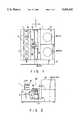
- FIG. 1is a schematic plan view showing a coating/developing apparatus according to an embodiment of the present invention
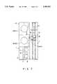
- FIG. 2is a schematic side view of the apparatus shown in FIG. 1;
- FIG. 3is a perspective view showing in detail a transfer robot according to the present invention.
- FIG. 4is a schematic front view showing the positional relationship between an arm and forks of the robot shown in FIG. 3;
- FIG. 5is a perspective view showing in detail a modification of the transfer robot according to the invention.
- FIG. 6is a schematic front view showing the positional relationship between an arm and forks of the robot shown in FIG. 5;
- FIG. 7is a schematic plan view showing a coating/developing apparatus according to another embodiment of the present invention.
- FIG. 8is a schematic plan view showing a coating/developing apparatus according to still another embodiment of the present invention.
- FIG. 9is a schematic plan view showing a coating/developing apparatus according to still another embodiment of the present invention.
- the apparatus shown in FIG. 1has a carrier station 1 provided with wafer carriers 2 and 3 for receiving semiconductor wafers w, or objects to be processed.
- the apparatusalso has a processing section 10 having two processing units 20 for processing wafers W, i.e. a resist liquid coating unit 21 and a developing liquid coating unit 22.
- the carrier station 1 and processing section 10face each other, and a transfer section 7 is interposed therebetween.
- An operation section 4is provided on the side of these sections 1, 7 and 10.
- the carrier station 1is provided with two wafer carrier 2 for receiving non-processed wafers W and two wafer carriers 3 for receiving processed wafers w.
- four transfer tables 5are situated just under the corresponding carriers 2 and 3.
- Each table 5is provided with fixed wafer support pins 6.
- the support pins 6are situated so as not to interfere with an arm 35 and forks 36 and 37 of a robot 30 (described later) and the pins 6 receive the wafers W from the arm 35 and forks 36 and 37.
- the transfer section 7comprises the robot 30 which is movable along a transfer path 31 provided between the carrier station 1 and processing section 10.
- the robot 30comprises a carriage table 32.
- the table 32is driven by a ball-screw mechanism (not shown) and it is moved along the transfer path 31.
- a shaft 33stands on the upper surface of the carriage table 32. The shaft 33 can be moved vertically and rotated horizontally by a ball-screw mechanism or a stepping motor built in the carriage table 32.
- a driving block 34is fixed on the top portion of the shaft 33.
- the block 34is provided with an arm 35 and two forks 36 and 37.
- the arm 35 and forks 36 and 37are coupled to driving means in the block 34 via associated support frames 35a, 36a and 37a.
- the arm 35 and forks 36 and 37are independently movable in a horizontal direction (indicated by arrow A in FIG. 3).
- a portion of the support frame 35a for the arm 35is put in the block 34 through an elongated opening 35b (see FIG. 3) formed in a lower portion of the right side plate (in FIG. 4) of the block 34.
- a portion of the support frame 36a of the fork 36is put in the block 34 through an elongated opening (not shown) formed at a substantially center portion of the left side plate (in FIG. 4) of the block 34.
- a portion of the support frame 37a of the fork 37is put in the block 34 through an elongated opening 37b (see FIG. 3) formed in the top plate of the block 34.
- the arm 35is used to load/unload wafers on/from the carriers 2 and 3.
- the width of a rectangular plate 41which is a main part of the arm 35, is determined so that the plate 41 can be inserted in the carrier 2, 3.
- Three suction holes 42 connected to a vacuum mechanismare formed in the plate 41, thereby drawing and holding wafers.
- the plate 41can be moved relative to a rear alignment frame 44 by a driving unit 43 provided at a rear part of the arm 35. Accordingly, when the plate 41 receives a wafer, the plate 41 is moved backward so that the wafer is clamped and aligned between a forward projection 45 of the plate 41 and the alignment frame 44.
- a wafer position sensor 46of, e.g. photoelectric type is provided on the alignment frame 44 of the arm 35.
- the forks 36 and 37are used to load/unload wafers on/from the processing units 20 (21, 22).
- each fork 36, 37is formed in a horseshoe shape, with an opened front portion.
- Each fork 36, 37has three claws 38 projecting from its inner peripheral surface at predetermined intervals. A lower edge portion of the wafer is held by the claws 38.
- a mapping sensor 39 for sensing the presence/absence of wafers in the carriers 2 and 3is attached at a front portion of the driving block 34.
- the sensor 39is constituted by a photosensor comprising a light-emitting portion 39a and a light-receiving portion 39b.
- the sensor 39is connected to driving means in the block 34 and it is movable horizontally (in the direction of arrow A in FIG. 3).
- the sensor 39can enter the wafer carrier 2, 3 from the state in which it faces the carrier 2, 3.
- the robot 30moves along the transfer path 31 to the position in front of the wafer carrier 2.
- the arm 35is moved vertically and also moved forward and backward by the driving mechanisms in the carriage table 32 and block 34, thereby taking out a non-processed wafer W from the carrier 2.
- the arm 35 holding the wafer Wis moved to the transfer table 5 below the carrier 2, and the arm 35 loads the wafer W on the table 5.
- the fork 36 or 37is moved and holds the wafer W on the table 5. Subsequently, the robot 30 is moved to the processing unit 20 (i.e. the resist liquid coating unit 21 or developing liquid coating unit 22). The fork 36, 37 is moved vertically and moved forward and backward by the driving mechanisms in the carriage table 32 and block 34, thereby transferring the wafer W to the processing unit 20.
- the processing unit 20i.e. the resist liquid coating unit 21 or developing liquid coating unit 22.
- the arm 35takes up another (second) non-processed wafer W and loads it on the transfer table 5.
- the fork 36, 37receives the wafer W from the table 5 and waits at the position facing the processing unit 20.
- the fork 36 or 37which does not hold the non-processed wafer w enters the processing unit 20 and holds the processed wafer w.
- the second wafer Wis loaded in the processing unit 20 by the other fork.
- the processed wafer W taken out from the processing unit 20is placed on the transfer table 5 below the carrier 3.
- the arm 35receives the wafer W from the table 5 and transfers it to the carrier 3.
- FIGS. 5 and 6show a modification of the transfer robot.
- a robot 30mcan transfer a wafer between the arm and fork, without using the transfer table 5.
- the parts common to those shown in FIGS. 3 and 4are denoted by like reference numerals and a description thereof is omitted.
- an arm 55 and forks 37 and 51are connected to driving means in the block 34 via associated support frames, in the same manner with the arm and forks shown in FIGS. 3 and 4.
- the arm 55 and forks 37, 51are independently movable horizontally (in the direction of arrow A in FIG. 5).
- the lower fork 37is the same as is employed in the preceding embodiment, but the upper fork 51 differs from the fork 36 in some respects.
- a portion of a support frame 51a of the fork 51is put in the block 34 through an elongated opening 51b (see FIG. 5) formed at a substantially center portion of the right side plate (in FIG. 6) of the block 34.
- a large notch 52 continuous with a center openingis formed at a proximal portion of the fork 51.
- the frame 51ais also provided with a notch matching with the notch 52. Since the notch 52 is provided, the fork 51 is provided with four claws 38 at four locations for supporting a wafer.
- the arm 55is connected to a left side portion (in FIG. 6) of the block 34 via support frames 56a and 56b including an extension actuator 57.
- the length and width of the arm 55are determined such that the arm 55 can pass through the center opening and notch 52 of the fork 51.
- the length of a rear alignment frame 59is set to be substantially equal to the width of the plate 41.
- the plate 41 of the arm 55can be moved relative to the alignment frame 59 by a driving unit 58.
- the wafercan be clamped and aligned between a front projection 45 of the plate 41 and the alignment frame 59.
- the arm 55receives the wafer W in the state in which the arm 55 is situated at the upper position and then the arm 55 is lowered by the actuator 57.
- the wafer wis transferred from the arm 55 on the fork 51.
- the fork 51receives the wafer W in the state in which the arm 55 is situated at the lower position and then the arm 55 is raised by the actuator 57.
- the wafer Wcan be transferred from the fork 51 to the arm 55.
- the transfer table 5is not required, and the space for installing the processing apparatus can be effectively used and the throughput can be enhanced.
- the fork 51can be made to be vertically movable. Further, both the fork 51 and arm 55 can be made to be vertically movable. Furthermore, the support frame of the lower fork 37 may be provided on the side portion of the block 34 and the fork 37 may be provided with a notch similar to that of the fork 51. Thereby, the arm 55 can be made to vertically movable through both forks 37 and 51.
- FIGS. 7 to 9show a modification of arrangement of the carrier station 1, processing section 10 and transfer section 7.
- the parts common to those of the embodiment of FIG. 1are denoted by the same reference numerals, and description thereof is omitted.
- the carrier station 1 and processing section 10are arranged along the same line.
- the transfer path 31 of the transfer section 7is parallel to the line of the carrier station 1 and processing section 10.
- the transfer tables 5are situated below the carriers 2 and 3, as shown in FIG. 2. By this arrangement, the transfer robot 30 does not need to rotate horizontally ( ⁇ -directional movement). Thus, the structure of the transfer section 7 is simplified, and the throughput is increased.
- the processing section 10comprises units 21 to 23, which are opposed to the carrier station 1 with the transfer section 7 interposed therebetween, and a unit 24 situated in line with the carrier station 1.
- the transfer tables 5are situated below the carriers 2 and 3, as shown in FIG. 2.
- the apparatuscan comprise many units 20, e.g. a plurality of units 21, 22 and 23 for coating a resist liquid or a developing liquid and the heat treatment unit 24.
- the carriers 2 and 3 of the carrier station 1 and the processing units 21 and 22 of the processing section 10are arranged along the rotational orbit of the transfer robot 30.
- the transfer tables 5are situated below the carriers 2 and 3, as shown in FIG. 2.
- the transfer table 5may be situated along the rotational orbit and at the same height as the carriers 2 and 3. According to the arrangement shown in FIG. 9, the transfer path of the transfer section 7 can be omitted, and the structure of the transfer section 7 can be simplified. In addition, the throughput can be increased.
- FIGS. 7 to 9show the case where the transfer robot 30 shown in FIGS. 3 and 4 is used.
- the transfer robot 30m shown in FIGS. 5 and 6may be used instead.
- the transfer table 5may be omitted, as stated above.
- the present inventionis applied to the coating/developing apparatus for semiconductor wafers.
- this inventionis applicable to processing apparatuses other than the coating/developing apparatus.
- this inventionis applicable to apparatuses for processing wafer-shaped objects, other than semiconductor wafers, such as LCD substrates, printed boards, photo marks, etc.
Landscapes
- Engineering & Computer Science (AREA)
- Physics & Mathematics (AREA)
- Condensed Matter Physics & Semiconductors (AREA)
- General Physics & Mathematics (AREA)
- Manufacturing & Machinery (AREA)
- Computer Hardware Design (AREA)
- Microelectronics & Electronic Packaging (AREA)
- Power Engineering (AREA)
- Container, Conveyance, Adherence, Positioning, Of Wafer (AREA)
- Warehouses Or Storage Devices (AREA)
Abstract
Description
Claims (21)
Priority Applications (1)
| Application Number | Priority Date | Filing Date | Title |
|---|---|---|---|
| US08/403,138US5460478A (en) | 1992-02-05 | 1995-03-13 | Method for processing wafer-shaped substrates |
Applications Claiming Priority (2)
| Application Number | Priority Date | Filing Date | Title |
|---|---|---|---|
| JP4047738AJP2867194B2 (en) | 1992-02-05 | 1992-02-05 | Processing device and processing method |
| JP4-047738 | 1992-02-05 |
Related Child Applications (1)
| Application Number | Title | Priority Date | Filing Date |
|---|---|---|---|
| US30245594ADivision | 1992-02-05 | 1994-09-09 |
Publications (1)
| Publication Number | Publication Date |
|---|---|
| US5364222Atrue US5364222A (en) | 1994-11-15 |
Family
ID=12783690
Family Applications (2)
| Application Number | Title | Priority Date | Filing Date |
|---|---|---|---|
| US08/014,161Expired - LifetimeUS5364222A (en) | 1992-02-05 | 1993-02-05 | Apparatus for processing wafer-shaped substrates |
| US08/403,138Expired - LifetimeUS5460478A (en) | 1992-02-05 | 1995-03-13 | Method for processing wafer-shaped substrates |
Family Applications After (1)
| Application Number | Title | Priority Date | Filing Date |
|---|---|---|---|
| US08/403,138Expired - LifetimeUS5460478A (en) | 1992-02-05 | 1995-03-13 | Method for processing wafer-shaped substrates |
Country Status (3)
| Country | Link |
|---|---|
| US (2) | US5364222A (en) |
| JP (1) | JP2867194B2 (en) |
| KR (1) | KR0177591B1 (en) |
Cited By (65)
| Publication number | Priority date | Publication date | Assignee | Title |
|---|---|---|---|---|
| US5562387A (en)* | 1993-10-04 | 1996-10-08 | Tokyo Electron Limited | Device for transferring plate-like objects |
| US5564889A (en)* | 1993-06-18 | 1996-10-15 | Tokyo Electron Limited | Semiconductor treatment system and method for exchanging and treating substrate |
| US5565034A (en)* | 1993-10-29 | 1996-10-15 | Tokyo Electron Limited | Apparatus for processing substrates having a film formed on a surface of the substrate |
| US5607276A (en)* | 1995-07-06 | 1997-03-04 | Brooks Automation, Inc. | Batchloader for substrate carrier on load lock |
| US5611655A (en)* | 1993-04-23 | 1997-03-18 | Tokyo Electron Limited | Vacuum process apparatus and vacuum processing method |
| US5613821A (en)* | 1995-07-06 | 1997-03-25 | Brooks Automation, Inc. | Cluster tool batchloader of substrate carrier |
| US5626675A (en)* | 1993-11-18 | 1997-05-06 | Tokyo Electron Limited | Resist processing apparatus, substrate processing apparatus and method of transferring a processed article |
| US5629044A (en)* | 1995-01-31 | 1997-05-13 | Nobler Technologies, Inc. | Compact disc coating and handling system |
| US5651823A (en)* | 1993-07-16 | 1997-07-29 | Semiconductor Systems, Inc. | Clustered photolithography system |
| US5664254A (en)* | 1995-02-02 | 1997-09-02 | Tokyo Electron Limited | Substrate processing apparatus and substrate processing method |
| US5841515A (en)* | 1995-09-27 | 1998-11-24 | Dainippon Screen Mfg. Co., Ltd. | Substrate container cassette, interface mechanism, and substrate processing |
| US5937223A (en)* | 1996-11-08 | 1999-08-10 | Tokyo Electron Limited | Processing apparatus |
| US5963753A (en)* | 1997-01-24 | 1999-10-05 | Dainippon Screen Mfg. Co., Ltd. | Substrate processing apparatus |
| US6036426A (en)* | 1996-01-26 | 2000-03-14 | Creative Design Corporation | Wafer handling method and apparatus |
| US6120229A (en)* | 1999-02-01 | 2000-09-19 | Brooks Automation Inc. | Substrate carrier as batchloader |
| US6132165A (en)* | 1998-02-23 | 2000-10-17 | Applied Materials, Inc. | Single drive, dual plane robot |
| US6176667B1 (en)* | 1996-04-30 | 2001-01-23 | Applied Materials, Inc. | Multideck wafer processing system |
| US6213708B1 (en)* | 1997-03-12 | 2001-04-10 | Advanced Micro Devices, Inc. | System for sorting multiple semiconductor wafers |
| EP0793262A3 (en)* | 1996-02-28 | 2001-08-16 | Applied Materials, Inc. | Multiple independent robot assembly and apparatus for processing and transferring semiconductor wafers |
| US20020033136A1 (en)* | 1999-04-02 | 2002-03-21 | Silicon Valley Group, Thermal Systems Llc. | Semiconductor wafer processing system with vertically-stacked process chambers and single-axis dual-wafer transfer system |
| US6450755B1 (en)* | 1998-07-10 | 2002-09-17 | Equipe Technologies | Dual arm substrate handling robot with a batch loader |
| US6473157B2 (en)* | 1992-02-07 | 2002-10-29 | Nikon Corporation | Method of manufacturing exposure apparatus and method for exposing a pattern on a mask onto a substrate |
| US6494666B2 (en)* | 2001-01-26 | 2002-12-17 | Fortrend Engineering Corporation | Simplified and enhanced SCARA arm |
| US6533531B1 (en) | 1998-12-29 | 2003-03-18 | Asml Us, Inc. | Device for handling wafers in microelectronic manufacturing |
| US20030086775A1 (en)* | 2001-11-08 | 2003-05-08 | Farhad Farassat | Mechanism for exchanging chip-carrier plates for use in a hybrid chip-bonding machine |
| EP1143488A3 (en)* | 1995-07-19 | 2003-10-29 | Hitachi, Ltd. | Vacuum processing apparatus and semiconductor manufacturing line using the same |
| US6652216B1 (en)* | 1998-05-05 | 2003-11-25 | Recif, S.A. | Method and device for changing a semiconductor wafer position |
| US20030219914A1 (en)* | 2002-01-29 | 2003-11-27 | Recif, S. A. | Apparatus and process for identification of characters inscribed on a semiconductor wafer containing an orientation mark |
| US20040005211A1 (en)* | 1996-02-28 | 2004-01-08 | Lowrance Robert B. | Multiple independent robot assembly and apparatus and control system for processing and transferring semiconductor wafers |
| US6707528B1 (en)* | 1994-03-02 | 2004-03-16 | Nikon Corporation | Exposure apparatus having independent chambers and methods of making the same |
| US6722834B1 (en)* | 1997-10-08 | 2004-04-20 | Applied Materials, Inc. | Robot blade with dual offset wafer supports |
| US6752585B2 (en) | 2001-06-13 | 2004-06-22 | Applied Materials Inc | Method and apparatus for transferring a semiconductor substrate |
| US20040213648A1 (en)* | 2003-04-14 | 2004-10-28 | Hofmeister Christopher A | Substrate cassette mapper |
| US20050006916A1 (en)* | 2003-06-27 | 2005-01-13 | Mattson Technology, Inc. | Endeffectors for handling semiconductor wafers |
| US20060251817A1 (en)* | 2005-05-06 | 2006-11-09 | Tokyo Electron Limited | Coating method and coating apparatus |
| US20060280586A1 (en)* | 2005-05-27 | 2006-12-14 | Innolux Display Corp. | Substrate conveyance apparatus |
| US20070114686A1 (en)* | 2002-11-13 | 2007-05-24 | Molecular Imprints, Inc. | Method for expelling gas positioned between a substrate and a mold |
| US20070228609A1 (en)* | 2006-04-03 | 2007-10-04 | Molecular Imprints, Inc. | Imprinting of Partial Fields at the Edge of the Wafer |
| US20070269302A1 (en)* | 2006-05-22 | 2007-11-22 | Naontech Co., Ltd. | Semiconductor material handling system |
| US20080260500A1 (en)* | 2007-02-27 | 2008-10-23 | Meulen Peter Van Der | Batch substrate handling |
| US7547398B2 (en) | 2006-04-18 | 2009-06-16 | Molecular Imprints, Inc. | Self-aligned process for fabricating imprint templates containing variously etched features |
| US20090156082A1 (en)* | 2007-12-14 | 2009-06-18 | Prime View International Co., Ltd. | Apparatus for Transferring Substrate |
| USD602882S1 (en) | 2006-03-30 | 2009-10-27 | Tokyo Electron Limited | Wafer carrying-in/out apparatus |
| US20090290967A1 (en)* | 2008-03-13 | 2009-11-26 | Jon Jamieson | End Effector |
| US7635263B2 (en) | 2005-01-31 | 2009-12-22 | Molecular Imprints, Inc. | Chucking system comprising an array of fluid chambers |
| US7635445B2 (en) | 2005-01-31 | 2009-12-22 | Molecular Imprints, Inc. | Method of separating a mold from a solidified layer disposed on a substrate |
| US7636999B2 (en) | 2005-01-31 | 2009-12-29 | Molecular Imprints, Inc. | Method of retaining a substrate to a wafer chuck |
| US7641840B2 (en)* | 2002-11-13 | 2010-01-05 | Molecular Imprints, Inc. | Method for expelling gas positioned between a substrate and a mold |
| US7670530B2 (en) | 2006-01-20 | 2010-03-02 | Molecular Imprints, Inc. | Patterning substrates employing multiple chucks |
| US7670529B2 (en) | 2005-12-08 | 2010-03-02 | Molecular Imprints, Inc. | Method and system for double-sided patterning of substrates |
| US7727453B2 (en) | 2002-07-11 | 2010-06-01 | Molecular Imprints, Inc. | Step and repeat imprint lithography processes |
| US7780893B2 (en) | 2006-04-03 | 2010-08-24 | Molecular Imprints, Inc. | Method of concurrently patterning a substrate having a plurality of fields and a plurality of alignment marks |
| US7803308B2 (en) | 2005-12-01 | 2010-09-28 | Molecular Imprints, Inc. | Technique for separating a mold from solidified imprinting material |
| US7906058B2 (en) | 2005-12-01 | 2011-03-15 | Molecular Imprints, Inc. | Bifurcated contact printing technique |
| US20110183411A1 (en)* | 2010-01-22 | 2011-07-28 | Highres Biosolutions | Self-sterilizing automated incubator |
| US8012395B2 (en) | 2006-04-18 | 2011-09-06 | Molecular Imprints, Inc. | Template having alignment marks formed of contrast material |
| US20110311340A1 (en)* | 2010-06-16 | 2011-12-22 | Tokyo Electron Limted | Substrate processing apparatus, substrate processing method and storage medium storing substrate processing program |
| US8142850B2 (en) | 2006-04-03 | 2012-03-27 | Molecular Imprints, Inc. | Patterning a plurality of fields on a substrate to compensate for differing evaporation times |
| US8215946B2 (en) | 2006-05-18 | 2012-07-10 | Molecular Imprints, Inc. | Imprint lithography system and method |
| EP2099061A3 (en)* | 1997-11-28 | 2013-06-12 | Mattson Technology, Inc. | Systems and methods for low contamination, high throughput handling of workpieces for vacuum processing |
| US8500388B2 (en) | 2003-11-10 | 2013-08-06 | Brooks Automation, Inc. | Semiconductor wafer handling and transport |
| US20160336212A1 (en)* | 2015-05-15 | 2016-11-17 | Suss Microtec Lithography Gmbh | Apparatus, system, and method for handling aligned wafer pairs |
| US10086511B2 (en) | 2003-11-10 | 2018-10-02 | Brooks Automation, Inc. | Semiconductor manufacturing systems |
| US10403528B2 (en)* | 2015-03-25 | 2019-09-03 | Kokusai Electric Corporation | Substrate-processing apparatus and method of manufacturing semiconductor device |
| US11183401B2 (en) | 2015-05-15 | 2021-11-23 | Suss Microtec Lithography Gmbh | System and related techniques for handling aligned substrate pairs |
Families Citing this family (87)
| Publication number | Priority date | Publication date | Assignee | Title |
|---|---|---|---|---|
| EP0843640A4 (en)* | 1995-07-07 | 2001-06-27 | Pri Automation Inc | Straight line wafer transfer system |
| US5741109A (en)* | 1995-07-07 | 1998-04-21 | Pri Automation, Inc. | Wafer transfer system having vertical lifting capability |
| US5647718A (en)* | 1995-07-07 | 1997-07-15 | Pri Automation, Inc. | Straight line wafer transfer system |
| US5615988A (en)* | 1995-07-07 | 1997-04-01 | Pri Automation, Inc. | Wafer transfer system having rotational capability |
| KR100244041B1 (en)* | 1995-08-05 | 2000-02-01 | 엔도 마코토 | Substrate processing apparatus |
| JP2747269B2 (en)* | 1996-02-21 | 1998-05-06 | 山形日本電気株式会社 | Box transport device |
| US5870488A (en)* | 1996-05-07 | 1999-02-09 | Fortrend Engineering Corporation | Method and apparatus for prealigning wafers in a wafer sorting system |
| US6752584B2 (en)* | 1996-07-15 | 2004-06-22 | Semitool, Inc. | Transfer devices for handling microelectronic workpieces within an environment of a processing machine and methods of manufacturing and using such devices in the processing of microelectronic workpieces |
| US6749390B2 (en)* | 1997-12-15 | 2004-06-15 | Semitool, Inc. | Integrated tools with transfer devices for handling microelectronic workpieces |
| US6672820B1 (en)* | 1996-07-15 | 2004-01-06 | Semitool, Inc. | Semiconductor processing apparatus having linear conveyer system |
| US6921467B2 (en)* | 1996-07-15 | 2005-07-26 | Semitool, Inc. | Processing tools, components of processing tools, and method of making and using same for electrochemical processing of microelectronic workpieces |
| US6203582B1 (en)* | 1996-07-15 | 2001-03-20 | Semitool, Inc. | Modular semiconductor workpiece processing tool |
| US6322119B1 (en) | 1999-07-09 | 2001-11-27 | Semitool, Inc. | Robots for microelectronic workpiece handling |
| US6749391B2 (en) | 1996-07-15 | 2004-06-15 | Semitool, Inc. | Microelectronic workpiece transfer devices and methods of using such devices in the processing of microelectronic workpieces |
| US6318951B1 (en) | 1999-07-09 | 2001-11-20 | Semitool, Inc. | Robots for microelectronic workpiece handling |
| JP3202929B2 (en)* | 1996-09-13 | 2001-08-27 | 東京エレクトロン株式会社 | Processing system |
| US6572320B2 (en)* | 1997-05-05 | 2003-06-03 | Semitool, Inc. | Robot for handling workpieces in an automated processing system |
| JPH1111663A (en)* | 1997-06-27 | 1999-01-19 | Tokyo Electron Ltd | Substrate conveying device |
| US6062961A (en)* | 1997-11-05 | 2000-05-16 | Aplex, Inc. | Wafer polishing head drive |
| US5957764A (en)* | 1997-11-05 | 1999-09-28 | Aplex, Inc. | Modular wafer polishing apparatus and method |
| US5947802A (en)* | 1997-11-05 | 1999-09-07 | Aplex, Inc. | Wafer shuttle system |
| US6257827B1 (en)* | 1997-12-01 | 2001-07-10 | Brooks Automation Inc. | Apparatus and method for transporting substrates |
| JP4178534B2 (en)* | 1997-12-24 | 2008-11-12 | 株式会社安川電機 | Substrate transfer robot |
| US6565729B2 (en) | 1998-03-20 | 2003-05-20 | Semitool, Inc. | Method for electrochemically depositing metal on a semiconductor workpiece |
| US6497801B1 (en) | 1998-07-10 | 2002-12-24 | Semitool Inc | Electroplating apparatus with segmented anode array |
| JP4035901B2 (en)* | 1998-10-09 | 2008-01-23 | 村田機械株式会社 | Plate material transfer device |
| US6358128B1 (en)* | 1999-03-05 | 2002-03-19 | Ebara Corporation | Polishing apparatus |
| US7438788B2 (en) | 1999-04-13 | 2008-10-21 | Semitool, Inc. | Apparatus and methods for electrochemical processing of microelectronic workpieces |
| US7189318B2 (en) | 1999-04-13 | 2007-03-13 | Semitool, Inc. | Tuning electrodes used in a reactor for electrochemically processing a microelectronic workpiece |
| US7020537B2 (en) | 1999-04-13 | 2006-03-28 | Semitool, Inc. | Tuning electrodes used in a reactor for electrochemically processing a microelectronic workpiece |
| US7585398B2 (en) | 1999-04-13 | 2009-09-08 | Semitool, Inc. | Chambers, systems, and methods for electrochemically processing microfeature workpieces |
| TWI226387B (en) | 1999-04-13 | 2005-01-11 | Semitool Inc | Workpiece processor having processing chamber with improved processing fluid flow |
| US6916412B2 (en) | 1999-04-13 | 2005-07-12 | Semitool, Inc. | Adaptable electrochemical processing chamber |
| US7264698B2 (en) | 1999-04-13 | 2007-09-04 | Semitool, Inc. | Apparatus and methods for electrochemical processing of microelectronic workpieces |
| US7351314B2 (en) | 2003-12-05 | 2008-04-01 | Semitool, Inc. | Chambers, systems, and methods for electrochemically processing microfeature workpieces |
| US7351315B2 (en) | 2003-12-05 | 2008-04-01 | Semitool, Inc. | Chambers, systems, and methods for electrochemically processing microfeature workpieces |
| US7160421B2 (en) | 1999-04-13 | 2007-01-09 | Semitool, Inc. | Turning electrodes used in a reactor for electrochemically processing a microelectronic workpiece |
| US6481951B1 (en) | 1999-09-16 | 2002-11-19 | Applied Materials, Inc. | Multiple sided robot blade for semiconductor processing equipment |
| US6364592B1 (en)* | 1999-12-01 | 2002-04-02 | Brooks Automation, Inc. | Small footprint carrier front end loader |
| EP1401617A1 (en) | 2000-09-01 | 2004-03-31 | Asyst Technologies, Inc. | Edge grip aligner with buffering capabilities |
| KR20020032057A (en)* | 2000-10-25 | 2002-05-03 | 고석태 | An apparatus for transferring/reversing a substrate, a system for transferring/reversing a substrate using the apparatus, and a method for transferring/reversing a substrate |
| US7334826B2 (en)* | 2001-07-13 | 2008-02-26 | Semitool, Inc. | End-effectors for handling microelectronic wafers |
| US7281741B2 (en)* | 2001-07-13 | 2007-10-16 | Semitool, Inc. | End-effectors for handling microelectronic workpieces |
| US7090751B2 (en) | 2001-08-31 | 2006-08-15 | Semitool, Inc. | Apparatus and methods for electrochemical processing of microelectronic workpieces |
| CN1996553A (en) | 2001-08-31 | 2007-07-11 | 阿赛斯特技术公司 | Unified frame for semiconductor material handling system |
| US7217076B2 (en) | 2001-08-31 | 2007-05-15 | Asyst Technologies, Inc. | Semiconductor material handling system |
| US7066707B1 (en) | 2001-08-31 | 2006-06-27 | Asyst Technologies, Inc. | Wafer engine |
| US20030159921A1 (en)* | 2002-02-22 | 2003-08-28 | Randy Harris | Apparatus with processing stations for manually and automatically processing microelectronic workpieces |
| US6991710B2 (en) | 2002-02-22 | 2006-01-31 | Semitool, Inc. | Apparatus for manually and automatically processing microelectronic workpieces |
| JP2003293134A (en)* | 2002-04-09 | 2003-10-15 | Tdk Corp | System and method for depositing thin film, and method for manufacturing electronic component using the system |
| US20060043750A1 (en)* | 2004-07-09 | 2006-03-02 | Paul Wirth | End-effectors for handling microfeature workpieces |
| US20070014656A1 (en)* | 2002-07-11 | 2007-01-18 | Harris Randy A | End-effectors and associated control and guidance systems and methods |
| US7114903B2 (en)* | 2002-07-16 | 2006-10-03 | Semitool, Inc. | Apparatuses and method for transferring and/or pre-processing microelectronic workpieces |
| US6976822B2 (en) | 2002-07-16 | 2005-12-20 | Semitool, Inc. | End-effectors and transfer devices for handling microelectronic workpieces |
| US7930061B2 (en) | 2002-08-31 | 2011-04-19 | Applied Materials, Inc. | Methods and apparatus for loading and unloading substrate carriers on moving conveyors using feedback |
| US7506746B2 (en) | 2002-08-31 | 2009-03-24 | Applied Materials, Inc. | System for transporting substrate carriers |
| US7684895B2 (en)* | 2002-08-31 | 2010-03-23 | Applied Materials, Inc. | Wafer loading station that automatically retracts from a moving conveyor in response to an unscheduled event |
| US7234584B2 (en) | 2002-08-31 | 2007-06-26 | Applied Materials, Inc. | System for transporting substrate carriers |
| US20040081546A1 (en) | 2002-08-31 | 2004-04-29 | Applied Materials, Inc. | Method and apparatus for supplying substrates to a processing tool |
| US7243003B2 (en) | 2002-08-31 | 2007-07-10 | Applied Materials, Inc. | Substrate carrier handler that unloads substrate carriers directly from a moving conveyor |
| KR20050038134A (en)* | 2003-10-21 | 2005-04-27 | 삼성전자주식회사 | Glass substrate stocking system |
| KR101106869B1 (en)* | 2003-11-13 | 2012-01-19 | 어플라이드 머티어리얼스, 인코포레이티드 | Wafer loading station automatically withdraws from moving conveyors in response to unscheduled events |
| US20070020080A1 (en)* | 2004-07-09 | 2007-01-25 | Paul Wirth | Transfer devices and methods for handling microfeature workpieces within an environment of a processing machine |
| US20070059153A1 (en)* | 2005-09-14 | 2007-03-15 | Applied Materials, Inc. | Methods and apparatus for a transport lift assembly |
| US20090099688A1 (en)* | 2005-11-10 | 2009-04-16 | Hugo Salamanca | Integral robot system and method for the dislodging process and/or anode handling from casting wheels |
| US20100057254A1 (en)* | 2006-11-13 | 2010-03-04 | Salamanca Hugo P | Methods for using robotics in mining and post-mining processing |
| US20070299556A1 (en)* | 2005-11-10 | 2007-12-27 | Hugo Salamanca | Robot system and method for scrap bundling in metal smelting and refining processes |
| US20070180678A1 (en)* | 2005-11-10 | 2007-08-09 | Hugo Salamanca | Robot system and method for bolt removal from SAG and/or ball mills in ore concentration processes |
| US7746018B2 (en)* | 2005-11-10 | 2010-06-29 | MI Robotic Solutions | Robot system and method for reposition and/or removal of base plates from cathode stripping machines in electrometallurgical processes |
| US20070152616A1 (en)* | 2005-11-10 | 2007-07-05 | Hugo Salamanca | Robot system and method for cathode selection and handling procedures after the harvest |
| US20070185610A1 (en)* | 2005-11-10 | 2007-08-09 | Hugo Salamanca | Robot system and method for the application of dislodging material and pin positioning in casting wheels |
| US20070267043A1 (en)* | 2005-11-10 | 2007-11-22 | Hugo Salamanca | Robot system and method for washing and unclogging procedures of machines under maintenance |
| US8418830B2 (en)* | 2005-11-10 | 2013-04-16 | Mi Robotic Solutions (Mirs) | Robot system and method for removing sticks and/or foreign elements from conveyor belts |
| US20070144894A1 (en)* | 2005-11-10 | 2007-06-28 | Hugo Salamanca | Robot system and method for cathode stripping in electrometallurgical and industrial processes |
| US20090177324A1 (en)* | 2005-11-10 | 2009-07-09 | Hugo Salamanca | Robot system and method for maxibags sampling in ore concentration processes |
| US20090101179A1 (en)* | 2005-11-10 | 2009-04-23 | Hugo Salamanca | Robot system and method for molybdenum roasting furnaces cleaning procedures |
| US20090121061A1 (en)* | 2005-11-10 | 2009-05-14 | Hugo Salamanca | Robot system and method for unblocking the primary crusher |
| US20070144006A1 (en)* | 2005-11-10 | 2007-06-28 | Hugo Salamanca | Robotic system and method for a transfer station for cathodes and/or base plates |
| US20080073569A1 (en)* | 2006-09-23 | 2008-03-27 | Varian Semiconductor Equipment Associates, Inc. | Mask position detection |
| US8277165B2 (en)* | 2007-09-22 | 2012-10-02 | Dynamic Micro System Semiconductor Equipment GmbH | Transfer mechanism with multiple wafer handling capability |
| US8430620B1 (en) | 2008-03-24 | 2013-04-30 | Novellus Systems, Inc. | Dedicated hot and cold end effectors for improved throughput |
| US20120136472A1 (en)* | 2010-11-25 | 2012-05-31 | Li Yan-Ze | Dual-arm type robotic arm and its method of transporting panels |
| US9570311B2 (en)* | 2012-02-10 | 2017-02-14 | Taiwan Semiconductor Manufacturing Company, Ltd. | Modular grinding apparatuses and methods for wafer thinning |
| US9245783B2 (en) | 2013-05-24 | 2016-01-26 | Novellus Systems, Inc. | Vacuum robot with linear translation carriage |
| US11421321B2 (en) | 2015-07-28 | 2022-08-23 | Asm Ip Holding B.V. | Apparatuses for thin film deposition |
| US10204790B2 (en) | 2015-07-28 | 2019-02-12 | Asm Ip Holding B.V. | Methods for thin film deposition |
| TWI889919B (en) | 2020-10-21 | 2025-07-11 | 荷蘭商Asm Ip私人控股有限公司 | Methods and aparatuses for flowable gap-fill |
Citations (14)
| Publication number | Priority date | Publication date | Assignee | Title |
|---|---|---|---|---|
| US4465416A (en)* | 1982-05-17 | 1984-08-14 | The Perkin-Elmer Corporation | Wafer handling mechanism |
| JPS62139341A (en)* | 1985-12-13 | 1987-06-23 | Plasma Syst:Kk | Treating device for substrate and wafer surface |
| JPS6464231A (en)* | 1987-09-03 | 1989-03-10 | Toshiba Corp | Conveyor |
| US4846623A (en)* | 1986-10-08 | 1989-07-11 | Dainippon Screen Mfg. Co., Ltd. | Wafer transferring device |
| JPH01305533A (en)* | 1988-06-03 | 1989-12-08 | Toshiba Corp | Conveyance device |
| JPH0271643A (en)* | 1988-09-07 | 1990-03-12 | Mitsubishi Electric Corp | Local area network |
| JPH02196414A (en)* | 1989-01-25 | 1990-08-03 | Fujitsu Ltd | Resist processing equipment |
| JPH034345A (en)* | 1989-05-31 | 1991-01-10 | Nec Corp | Hard disk device having id part backup function |
| US4985722A (en)* | 1988-02-12 | 1991-01-15 | Tokyo Electron Limited | Apparatus for coating a photo-resist film and/or developing it after being exposed |
| US5083896A (en)* | 1988-09-16 | 1992-01-28 | Tokyo Ohka Kogyo Co., Ltd. | Object handling device |
| EP0468409A1 (en)* | 1990-07-23 | 1992-01-29 | Dainippon Screen Mfg. Co., Ltd. | Interface apparatus for transporting substrates between substrate processing apparatus |
| US5133635A (en)* | 1990-03-05 | 1992-07-28 | Tet Techno Investment Trust Settlement | Method and apparatus for holding and conveying platelike substrates |
| US5183370A (en)* | 1989-12-29 | 1993-02-02 | Commissariat A L'energie Atomique | Apparatus for placing or storing flat articles in a cassette with intermediate racks |
| US5217340A (en)* | 1989-01-28 | 1993-06-08 | Kokusai Electric Co., Ltd. | Wafer transfer mechanism in vertical CVD diffusion apparatus |
Family Cites Families (7)
| Publication number | Priority date | Publication date | Assignee | Title |
|---|---|---|---|---|
| US3832836A (en)* | 1973-11-28 | 1974-09-03 | Deere & Co | Harvester roll structure |
| DE3219502C2 (en)* | 1982-05-25 | 1990-04-19 | Ernst Leitz Wetzlar Gmbh, 6330 Wetzlar | Device for the automatic transport of disc-shaped objects |
| JPH0622258B2 (en)* | 1987-07-24 | 1994-03-23 | 日立電子エンジニアリング株式会社 | Wafer surface inspection device |
| JPS6440739A (en)* | 1987-08-05 | 1989-02-13 | Tochigi Fuji Sangyo Kk | Power transmitter |
| JP2659384B2 (en)* | 1988-02-16 | 1997-09-30 | オリンパス光学工業株式会社 | Wafer inspection equipment |
| JPH03289132A (en)* | 1990-04-06 | 1991-12-19 | Hitachi Ltd | surface treatment equipment |
| US5256204A (en)* | 1991-12-13 | 1993-10-26 | United Microelectronics Corporation | Single semiconductor water transfer method and manufacturing system |
- 1992
- 1992-02-05JPJP4047738Apatent/JP2867194B2/ennot_activeExpired - Lifetime
- 1993
- 1993-02-05KRKR1019930001597Apatent/KR0177591B1/ennot_activeExpired - Lifetime
- 1993-02-05USUS08/014,161patent/US5364222A/ennot_activeExpired - Lifetime
- 1995
- 1995-03-13USUS08/403,138patent/US5460478A/ennot_activeExpired - Lifetime
Patent Citations (14)
| Publication number | Priority date | Publication date | Assignee | Title |
|---|---|---|---|---|
| US4465416A (en)* | 1982-05-17 | 1984-08-14 | The Perkin-Elmer Corporation | Wafer handling mechanism |
| JPS62139341A (en)* | 1985-12-13 | 1987-06-23 | Plasma Syst:Kk | Treating device for substrate and wafer surface |
| US4846623A (en)* | 1986-10-08 | 1989-07-11 | Dainippon Screen Mfg. Co., Ltd. | Wafer transferring device |
| JPS6464231A (en)* | 1987-09-03 | 1989-03-10 | Toshiba Corp | Conveyor |
| US4985722A (en)* | 1988-02-12 | 1991-01-15 | Tokyo Electron Limited | Apparatus for coating a photo-resist film and/or developing it after being exposed |
| JPH01305533A (en)* | 1988-06-03 | 1989-12-08 | Toshiba Corp | Conveyance device |
| JPH0271643A (en)* | 1988-09-07 | 1990-03-12 | Mitsubishi Electric Corp | Local area network |
| US5083896A (en)* | 1988-09-16 | 1992-01-28 | Tokyo Ohka Kogyo Co., Ltd. | Object handling device |
| JPH02196414A (en)* | 1989-01-25 | 1990-08-03 | Fujitsu Ltd | Resist processing equipment |
| US5217340A (en)* | 1989-01-28 | 1993-06-08 | Kokusai Electric Co., Ltd. | Wafer transfer mechanism in vertical CVD diffusion apparatus |
| JPH034345A (en)* | 1989-05-31 | 1991-01-10 | Nec Corp | Hard disk device having id part backup function |
| US5183370A (en)* | 1989-12-29 | 1993-02-02 | Commissariat A L'energie Atomique | Apparatus for placing or storing flat articles in a cassette with intermediate racks |
| US5133635A (en)* | 1990-03-05 | 1992-07-28 | Tet Techno Investment Trust Settlement | Method and apparatus for holding and conveying platelike substrates |
| EP0468409A1 (en)* | 1990-07-23 | 1992-01-29 | Dainippon Screen Mfg. Co., Ltd. | Interface apparatus for transporting substrates between substrate processing apparatus |
Cited By (107)
| Publication number | Priority date | Publication date | Assignee | Title |
|---|---|---|---|---|
| US6473157B2 (en)* | 1992-02-07 | 2002-10-29 | Nikon Corporation | Method of manufacturing exposure apparatus and method for exposing a pattern on a mask onto a substrate |
| US5611655A (en)* | 1993-04-23 | 1997-03-18 | Tokyo Electron Limited | Vacuum process apparatus and vacuum processing method |
| US5564889A (en)* | 1993-06-18 | 1996-10-15 | Tokyo Electron Limited | Semiconductor treatment system and method for exchanging and treating substrate |
| US5651823A (en)* | 1993-07-16 | 1997-07-29 | Semiconductor Systems, Inc. | Clustered photolithography system |
| US5655871A (en)* | 1993-10-04 | 1997-08-12 | Tokyo Electron Limited | Device for transferring plate-like objects |
| US5562387A (en)* | 1993-10-04 | 1996-10-08 | Tokyo Electron Limited | Device for transferring plate-like objects |
| US5565034A (en)* | 1993-10-29 | 1996-10-15 | Tokyo Electron Limited | Apparatus for processing substrates having a film formed on a surface of the substrate |
| US5626675A (en)* | 1993-11-18 | 1997-05-06 | Tokyo Electron Limited | Resist processing apparatus, substrate processing apparatus and method of transferring a processed article |
| US6707528B1 (en)* | 1994-03-02 | 2004-03-16 | Nikon Corporation | Exposure apparatus having independent chambers and methods of making the same |
| US5629044A (en)* | 1995-01-31 | 1997-05-13 | Nobler Technologies, Inc. | Compact disc coating and handling system |
| US5698030A (en)* | 1995-01-31 | 1997-12-16 | Nobler Technologies, Inc. | Compact disc coating and handling system |
| US5664254A (en)* | 1995-02-02 | 1997-09-02 | Tokyo Electron Limited | Substrate processing apparatus and substrate processing method |
| USRE37470E1 (en)* | 1995-02-02 | 2001-12-18 | Tokyo Electron Limited | Substrate processing apparatus and substrate processing method |
| US5613821A (en)* | 1995-07-06 | 1997-03-25 | Brooks Automation, Inc. | Cluster tool batchloader of substrate carrier |
| US5607276A (en)* | 1995-07-06 | 1997-03-04 | Brooks Automation, Inc. | Batchloader for substrate carrier on load lock |
| EP1143488A3 (en)* | 1995-07-19 | 2003-10-29 | Hitachi, Ltd. | Vacuum processing apparatus and semiconductor manufacturing line using the same |
| US20080138180A1 (en)* | 1995-07-19 | 2008-06-12 | Minoru Soraoka | Vacuum processing apparatus and semiconductor manufacturing line using the same |
| US20090220322A1 (en)* | 1995-07-19 | 2009-09-03 | Minoru Soraoka | Vacuum Processing Apparatus And Semiconductor Manufacturing Line Using The Same |
| US6752580B2 (en) | 1995-07-19 | 2004-06-22 | Hitachi, Ltd. | Vacuum processing apparatus and semiconductor manufacturing line using the same |
| US20050175435A1 (en)* | 1995-07-19 | 2005-08-11 | Minoru Soraoka | Vacuum processing apparatus and semiconductor manufacturing line using the same |
| US6752579B2 (en) | 1995-07-19 | 2004-06-22 | Hitachi, Ltd. | Vacuum processing apparatus and semiconductor manufacturing line using the same |
| US7347656B2 (en) | 1995-07-19 | 2008-03-25 | Hitachi, Ltd. | Vacuum processing apparatus and semiconductor manufacturing line using the same |
| US6895685B2 (en) | 1995-07-19 | 2005-05-24 | Hitachi, Ltd. | Vacuum processing apparatus and semiconductor manufacturing line using the same |
| US20040197169A1 (en)* | 1995-07-19 | 2004-10-07 | Minoru Soraoka | Vacuum processing apparatus and semiconductor manufacturing line using the same |
| US20040118005A1 (en)* | 1995-07-19 | 2004-06-24 | Minoru Soraoka | Vacuum processing apparatus and semiconductor manufacturing line using the same |
| US5841515A (en)* | 1995-09-27 | 1998-11-24 | Dainippon Screen Mfg. Co., Ltd. | Substrate container cassette, interface mechanism, and substrate processing |
| US6036426A (en)* | 1996-01-26 | 2000-03-14 | Creative Design Corporation | Wafer handling method and apparatus |
| EP0793262A3 (en)* | 1996-02-28 | 2001-08-16 | Applied Materials, Inc. | Multiple independent robot assembly and apparatus for processing and transferring semiconductor wafers |
| US20040005211A1 (en)* | 1996-02-28 | 2004-01-08 | Lowrance Robert B. | Multiple independent robot assembly and apparatus and control system for processing and transferring semiconductor wafers |
| US6176667B1 (en)* | 1996-04-30 | 2001-01-23 | Applied Materials, Inc. | Multideck wafer processing system |
| US5937223A (en)* | 1996-11-08 | 1999-08-10 | Tokyo Electron Limited | Processing apparatus |
| US5963753A (en)* | 1997-01-24 | 1999-10-05 | Dainippon Screen Mfg. Co., Ltd. | Substrate processing apparatus |
| US6213708B1 (en)* | 1997-03-12 | 2001-04-10 | Advanced Micro Devices, Inc. | System for sorting multiple semiconductor wafers |
| US6722834B1 (en)* | 1997-10-08 | 2004-04-20 | Applied Materials, Inc. | Robot blade with dual offset wafer supports |
| EP2099061A3 (en)* | 1997-11-28 | 2013-06-12 | Mattson Technology, Inc. | Systems and methods for low contamination, high throughput handling of workpieces for vacuum processing |
| US6132165A (en)* | 1998-02-23 | 2000-10-17 | Applied Materials, Inc. | Single drive, dual plane robot |
| US7108476B2 (en) | 1998-05-05 | 2006-09-19 | Recif Technologies Sas | Method and device for changing a semiconductor wafer position |
| US6652216B1 (en)* | 1998-05-05 | 2003-11-25 | Recif, S.A. | Method and device for changing a semiconductor wafer position |
| US20040091343A1 (en)* | 1998-05-05 | 2004-05-13 | Recif, Inc. | Method and device for changing a semiconductor wafer position |
| US6450755B1 (en)* | 1998-07-10 | 2002-09-17 | Equipe Technologies | Dual arm substrate handling robot with a batch loader |
| US6632065B1 (en) | 1998-07-10 | 2003-10-14 | Equipe Technologies | Substrate handling robot with a batch loader and individual vacuum control at batch loader paddles |
| US6533531B1 (en) | 1998-12-29 | 2003-03-18 | Asml Us, Inc. | Device for handling wafers in microelectronic manufacturing |
| US6120229A (en)* | 1999-02-01 | 2000-09-19 | Brooks Automation Inc. | Substrate carrier as batchloader |
| US6846149B2 (en)* | 1999-04-02 | 2005-01-25 | Aviza Technology, Inc. | Semiconductor wafer processing system with vertically-stacked process chambers and single-axis dual-wafer transfer system |
| US20020033136A1 (en)* | 1999-04-02 | 2002-03-21 | Silicon Valley Group, Thermal Systems Llc. | Semiconductor wafer processing system with vertically-stacked process chambers and single-axis dual-wafer transfer system |
| US6494666B2 (en)* | 2001-01-26 | 2002-12-17 | Fortrend Engineering Corporation | Simplified and enhanced SCARA arm |
| US6752585B2 (en) | 2001-06-13 | 2004-06-22 | Applied Materials Inc | Method and apparatus for transferring a semiconductor substrate |
| US7153088B2 (en) | 2001-06-13 | 2006-12-26 | Applied Materials, Inc. | Method and apparatus for transferring a semiconductor substrate |
| US20030086775A1 (en)* | 2001-11-08 | 2003-05-08 | Farhad Farassat | Mechanism for exchanging chip-carrier plates for use in a hybrid chip-bonding machine |
| US7156602B2 (en)* | 2001-11-08 | 2007-01-02 | F & K Delvotec Bondtechnick Gmbh | Mechanism for exchanging chip-carrier plates for use in a hybrid chip-bonding machine |
| US6961639B2 (en) | 2002-01-29 | 2005-11-01 | Recif, Societe Anonyme | Apparatus and process for identification of characters inscribed on a semiconductor wafer containing an orientation mark |
| US20030219914A1 (en)* | 2002-01-29 | 2003-11-27 | Recif, S. A. | Apparatus and process for identification of characters inscribed on a semiconductor wafer containing an orientation mark |
| US7727453B2 (en) | 2002-07-11 | 2010-06-01 | Molecular Imprints, Inc. | Step and repeat imprint lithography processes |
| US20070114686A1 (en)* | 2002-11-13 | 2007-05-24 | Molecular Imprints, Inc. | Method for expelling gas positioned between a substrate and a mold |
| US8282383B2 (en)* | 2002-11-13 | 2012-10-09 | Molecular Imprints, Inc. | Method for expelling gas positioned between a substrate and a mold |
| US7641840B2 (en)* | 2002-11-13 | 2010-01-05 | Molecular Imprints, Inc. | Method for expelling gas positioned between a substrate and a mold |
| US7691313B2 (en)* | 2002-11-13 | 2010-04-06 | Molecular Imprints, Inc. | Method for expelling gas positioned between a substrate and a mold |
| US20040213648A1 (en)* | 2003-04-14 | 2004-10-28 | Hofmeister Christopher A | Substrate cassette mapper |
| US7255524B2 (en)* | 2003-04-14 | 2007-08-14 | Brooks Automation, Inc. | Substrate cassette mapper |
| US8109549B2 (en) | 2003-06-27 | 2012-02-07 | Mattson Technology, Inc. | Endeffectors for handling semiconductor wafers |
| US20050006916A1 (en)* | 2003-06-27 | 2005-01-13 | Mattson Technology, Inc. | Endeffectors for handling semiconductor wafers |
| US20100096869A1 (en)* | 2003-06-27 | 2010-04-22 | Mattson Thermal Products Gmbh | Endeffectors for handling semiconductor wafers |
| US8622451B2 (en) | 2003-06-27 | 2014-01-07 | Mattson Technology, Inc. | Endeffectors for handling semiconductor wafers |
| US7654596B2 (en) | 2003-06-27 | 2010-02-02 | Mattson Technology, Inc. | Endeffectors for handling semiconductor wafers |
| US8500388B2 (en) | 2003-11-10 | 2013-08-06 | Brooks Automation, Inc. | Semiconductor wafer handling and transport |
| US8672605B2 (en) | 2003-11-10 | 2014-03-18 | Brooks Automation, Inc. | Semiconductor wafer handling and transport |
| US10086511B2 (en) | 2003-11-10 | 2018-10-02 | Brooks Automation, Inc. | Semiconductor manufacturing systems |
| US7636999B2 (en) | 2005-01-31 | 2009-12-29 | Molecular Imprints, Inc. | Method of retaining a substrate to a wafer chuck |
| US7635445B2 (en) | 2005-01-31 | 2009-12-22 | Molecular Imprints, Inc. | Method of separating a mold from a solidified layer disposed on a substrate |
| US7635263B2 (en) | 2005-01-31 | 2009-12-22 | Molecular Imprints, Inc. | Chucking system comprising an array of fluid chambers |
| US7678417B2 (en) | 2005-05-06 | 2010-03-16 | Tokyo Electron Limited | Coating method and coating apparatus |
| US20060251817A1 (en)* | 2005-05-06 | 2006-11-09 | Tokyo Electron Limited | Coating method and coating apparatus |
| US20060280586A1 (en)* | 2005-05-27 | 2006-12-14 | Innolux Display Corp. | Substrate conveyance apparatus |
| US7906058B2 (en) | 2005-12-01 | 2011-03-15 | Molecular Imprints, Inc. | Bifurcated contact printing technique |
| US7803308B2 (en) | 2005-12-01 | 2010-09-28 | Molecular Imprints, Inc. | Technique for separating a mold from solidified imprinting material |
| US7670529B2 (en) | 2005-12-08 | 2010-03-02 | Molecular Imprints, Inc. | Method and system for double-sided patterning of substrates |
| US7670530B2 (en) | 2006-01-20 | 2010-03-02 | Molecular Imprints, Inc. | Patterning substrates employing multiple chucks |
| USD607424S1 (en)* | 2006-03-30 | 2010-01-05 | Tokyo Electron Limited | Wafer carrying-in/out apparatus |
| USD602882S1 (en) | 2006-03-30 | 2009-10-27 | Tokyo Electron Limited | Wafer carrying-in/out apparatus |
| US7802978B2 (en) | 2006-04-03 | 2010-09-28 | Molecular Imprints, Inc. | Imprinting of partial fields at the edge of the wafer |
| US7780893B2 (en) | 2006-04-03 | 2010-08-24 | Molecular Imprints, Inc. | Method of concurrently patterning a substrate having a plurality of fields and a plurality of alignment marks |
| US8142850B2 (en) | 2006-04-03 | 2012-03-27 | Molecular Imprints, Inc. | Patterning a plurality of fields on a substrate to compensate for differing evaporation times |
| US20070228609A1 (en)* | 2006-04-03 | 2007-10-04 | Molecular Imprints, Inc. | Imprinting of Partial Fields at the Edge of the Wafer |
| US7547398B2 (en) | 2006-04-18 | 2009-06-16 | Molecular Imprints, Inc. | Self-aligned process for fabricating imprint templates containing variously etched features |
| US8012395B2 (en) | 2006-04-18 | 2011-09-06 | Molecular Imprints, Inc. | Template having alignment marks formed of contrast material |
| US8215946B2 (en) | 2006-05-18 | 2012-07-10 | Molecular Imprints, Inc. | Imprint lithography system and method |
| US20070269302A1 (en)* | 2006-05-22 | 2007-11-22 | Naontech Co., Ltd. | Semiconductor material handling system |
| US7661921B2 (en)* | 2006-05-22 | 2010-02-16 | Naontech Co., Ltd. | Semiconductor material handling system |
| US8950998B2 (en)* | 2007-02-27 | 2015-02-10 | Brooks Automation, Inc. | Batch substrate handling |
| US20080260500A1 (en)* | 2007-02-27 | 2008-10-23 | Meulen Peter Van Der | Batch substrate handling |
| US20090156082A1 (en)* | 2007-12-14 | 2009-06-18 | Prime View International Co., Ltd. | Apparatus for Transferring Substrate |
| US8182009B2 (en)* | 2008-03-13 | 2012-05-22 | Xyratex Technology, Ltd. | End effector |
| US20090290967A1 (en)* | 2008-03-13 | 2009-11-26 | Jon Jamieson | End Effector |
| US8759084B2 (en) | 2010-01-22 | 2014-06-24 | Michael J. Nichols | Self-sterilizing automated incubator |
| US20110183411A1 (en)* | 2010-01-22 | 2011-07-28 | Highres Biosolutions | Self-sterilizing automated incubator |
| US8845262B2 (en)* | 2010-06-16 | 2014-09-30 | Tokyo Electron Limited | Substrate processing apparatus, substrate processing method and storage medium storing substrate processing program |
| US20110311340A1 (en)* | 2010-06-16 | 2011-12-22 | Tokyo Electron Limted | Substrate processing apparatus, substrate processing method and storage medium storing substrate processing program |
| US10403528B2 (en)* | 2015-03-25 | 2019-09-03 | Kokusai Electric Corporation | Substrate-processing apparatus and method of manufacturing semiconductor device |
| CN106158706A (en)* | 2015-05-15 | 2016-11-23 | 苏斯微技术光刻有限公司 | For the method operating alignment wafer pair |
| CN106158714A (en)* | 2015-05-15 | 2016-11-23 | 苏斯微技术光刻有限公司 | For operating the device of alignment wafer pair |
| US20160336212A1 (en)* | 2015-05-15 | 2016-11-17 | Suss Microtec Lithography Gmbh | Apparatus, system, and method for handling aligned wafer pairs |
| US10825705B2 (en)* | 2015-05-15 | 2020-11-03 | Suss Microtec Lithography Gmbh | Apparatus, system, and method for handling aligned wafer pairs |
| CN106158706B (en)* | 2015-05-15 | 2020-11-13 | 苏斯微技术光刻有限公司 | Method for handling aligned wafer pairs |
| CN106158714B (en)* | 2015-05-15 | 2020-12-11 | 苏斯微技术光刻有限公司 | Apparatus for handling aligned wafer pairs |
| TWI718149B (en)* | 2015-05-15 | 2021-02-11 | 德商蘇士微科技印刷術股份有限公司 | Apparatus and system for handling aligned wafer pairs |
| US11183401B2 (en) | 2015-05-15 | 2021-11-23 | Suss Microtec Lithography Gmbh | System and related techniques for handling aligned substrate pairs |
| US11651983B2 (en) | 2015-05-15 | 2023-05-16 | Suss Microtec Lithography Gmbh | Apparatus, system, and method for handling aligned wafer pairs |
Also Published As
| Publication number | Publication date |
|---|---|
| JP2867194B2 (en) | 1999-03-08 |
| US5460478A (en) | 1995-10-24 |
| KR930018700A (en) | 1993-09-22 |
| KR0177591B1 (en) | 1999-04-15 |
| JPH06127609A (en) | 1994-05-10 |
Similar Documents
| Publication | Publication Date | Title |
|---|---|---|
| US5364222A (en) | Apparatus for processing wafer-shaped substrates | |
| KR101139180B1 (en) | Substrate transportation method and substrate transportation device | |
| KR102157427B1 (en) | Substrate transfer robot and substrate processing system | |
| KR101515247B1 (en) | Substrate processing apparatus | |
| JP3566475B2 (en) | Processing equipment | |
| KR940005974A (en) | Vacuum processing equipment | |
| KR20000023251A (en) | Substrate processing apparatus and substrate processing method | |
| JP2004241702A (en) | Device and method for substrate processing | |
| US6264705B1 (en) | Processing system | |
| JPH06246658A (en) | Substrate conveyer | |
| KR102396204B1 (en) | Substrate processing apparatus and substrate transporting method | |
| JP3446158B2 (en) | Substrate transfer processing equipment | |
| JPH05129417A (en) | Processing equipment of tabular body | |
| JP3912478B2 (en) | Substrate transfer device | |
| JP2743274B2 (en) | Substrate processing device and substrate transfer device | |
| KR20100094361A (en) | Substrate processing system | |
| JP2926592B2 (en) | Substrate processing equipment | |
| JP3246659B2 (en) | Resist processing apparatus, liquid processing apparatus, and substrate processing apparatus | |
| JP3205525B2 (en) | Substrate unloading device, loading device and unloading and loading device | |
| JP2926213B2 (en) | Substrate processing equipment | |
| JPH053241A (en) | Conveyer for plate-shaped object | |
| JPH0826413A (en) | Conveying mechanism and conveying method of platelike object | |
| US6854948B1 (en) | Stage with two substrate buffer station | |
| KR100572318B1 (en) | Transfer device for unloading semiconductor substrate from container | |
| JPH08264621A (en) | Processing method and processing device |
Legal Events
| Date | Code | Title | Description |
|---|---|---|---|
| AS | Assignment | Owner name:TOKYO ELECTRON KYUSHU LIMITED Free format text:ASSIGNMENT OF ASSIGNORS INTEREST;ASSIGNORS:AKIMOTO, MASAMI;YOSHIOKA, KAZUTOSHI;IIDA, NARUAKI;REEL/FRAME:006586/0228 Effective date:19930210 Owner name:TOKYO ELECTRON LIMITED Free format text:ASSIGNMENT OF ASSIGNORS INTEREST;ASSIGNORS:AKIMOTO, MASAMI;YOSHIOKA, KAZUTOSHI;IIDA, NARUAKI;REEL/FRAME:006586/0228 Effective date:19930210 | |
| STCF | Information on status: patent grant | Free format text:PATENTED CASE | |
| FEPP | Fee payment procedure | Free format text:PAYOR NUMBER ASSIGNED (ORIGINAL EVENT CODE: ASPN); ENTITY STATUS OF PATENT OWNER: LARGE ENTITY | |
| FPAY | Fee payment | Year of fee payment:4 | |
| AS | Assignment | Owner name:TOKYO ELECTRON LIMITED, JAPAN Free format text:ASSIGNMENT OF ASSIGNORS INTEREST;ASSIGNOR:TOKYO ELECTRON KYUSHU LIMITED;REEL/FRAME:009453/0220 Effective date:19980513 | |
| FEPP | Fee payment procedure | Free format text:PAYER NUMBER DE-ASSIGNED (ORIGINAL EVENT CODE: RMPN); ENTITY STATUS OF PATENT OWNER: LARGE ENTITY Free format text:PAYOR NUMBER ASSIGNED (ORIGINAL EVENT CODE: ASPN); ENTITY STATUS OF PATENT OWNER: LARGE ENTITY | |
| FPAY | Fee payment | Year of fee payment:8 | |
| FPAY | Fee payment | Year of fee payment:12 |