US5360981A - Amorphous silicon memory - Google Patents
Amorphous silicon memoryDownload PDFInfo
- Publication number
- US5360981A US5360981AUS08/194,628US19462894AUS5360981AUS 5360981 AUS5360981 AUS 5360981AUS 19462894 AUS19462894 AUS 19462894AUS 5360981 AUS5360981 AUS 5360981A
- Authority
- US
- United States
- Prior art keywords
- layer
- resistance
- voltage
- amorphous silicon
- analog memory
- Prior art date
- Legal status (The legal status is an assumption and is not a legal conclusion. Google has not performed a legal analysis and makes no representation as to the accuracy of the status listed.)
- Expired - Lifetime
Links
Images


Classifications
- H—ELECTRICITY
- H10—SEMICONDUCTOR DEVICES; ELECTRIC SOLID-STATE DEVICES NOT OTHERWISE PROVIDED FOR
- H10N—ELECTRIC SOLID-STATE DEVICES NOT OTHERWISE PROVIDED FOR
- H10N70/00—Solid-state devices having no potential barriers, and specially adapted for rectifying, amplifying, oscillating or switching
- H10N70/20—Multistable switching devices, e.g. memristors
- H10N70/25—Multistable switching devices, e.g. memristors based on bulk electronic defects, e.g. trapping of electrons
- H—ELECTRICITY
- H10—SEMICONDUCTOR DEVICES; ELECTRIC SOLID-STATE DEVICES NOT OTHERWISE PROVIDED FOR
- H10N—ELECTRIC SOLID-STATE DEVICES NOT OTHERWISE PROVIDED FOR
- H10N70/00—Solid-state devices having no potential barriers, and specially adapted for rectifying, amplifying, oscillating or switching
- H10N70/011—Manufacture or treatment of multistable switching devices
- H10N70/021—Formation of switching materials, e.g. deposition of layers
- H10N70/023—Formation of switching materials, e.g. deposition of layers by chemical vapor deposition, e.g. MOCVD, ALD
- H—ELECTRICITY
- H10—SEMICONDUCTOR DEVICES; ELECTRIC SOLID-STATE DEVICES NOT OTHERWISE PROVIDED FOR
- H10N—ELECTRIC SOLID-STATE DEVICES NOT OTHERWISE PROVIDED FOR
- H10N70/00—Solid-state devices having no potential barriers, and specially adapted for rectifying, amplifying, oscillating or switching
- H10N70/801—Constructional details of multistable switching devices
- H10N70/821—Device geometry
- H10N70/826—Device geometry adapted for essentially vertical current flow, e.g. sandwich or pillar type devices
- H—ELECTRICITY
- H10—SEMICONDUCTOR DEVICES; ELECTRIC SOLID-STATE DEVICES NOT OTHERWISE PROVIDED FOR
- H10N—ELECTRIC SOLID-STATE DEVICES NOT OTHERWISE PROVIDED FOR
- H10N70/00—Solid-state devices having no potential barriers, and specially adapted for rectifying, amplifying, oscillating or switching
- H10N70/801—Constructional details of multistable switching devices
- H10N70/881—Switching materials
- H10N70/884—Switching materials based on at least one element of group IIIA, IVA or VA, e.g. elemental or compound semiconductors
- Y—GENERAL TAGGING OF NEW TECHNOLOGICAL DEVELOPMENTS; GENERAL TAGGING OF CROSS-SECTIONAL TECHNOLOGIES SPANNING OVER SEVERAL SECTIONS OF THE IPC; TECHNICAL SUBJECTS COVERED BY FORMER USPC CROSS-REFERENCE ART COLLECTIONS [XRACs] AND DIGESTS
- Y10—TECHNICAL SUBJECTS COVERED BY FORMER USPC
- Y10S—TECHNICAL SUBJECTS COVERED BY FORMER USPC CROSS-REFERENCE ART COLLECTIONS [XRACs] AND DIGESTS
- Y10S438/00—Semiconductor device manufacturing: process
- Y10S438/90—Bulk effect device making
Definitions
- the present inventionrelates to novel semiconductor devices capable of being set and reset to a plurality of different conductance states.
- analogue memory devicecapable of being set and reset into a resistance which is a measure of a voltage applied to it and which comprises
- a metal top contact deposited on s aid amorphous silicon layerthe metal being one of V, Co, Ni, Pd, Fe or Mn;
- the nature of the first conducting layeris not critical as long as it is possible to grow the required amorphous silicon (a-Si) layer upon it.
- suitable materialsare Cr or V.
- unsuitable materialsare gold (which diffuses into the a-Si layer and mercury (which is liquid).
- the first conducting layerneed not extend on the whole area of the amorphous silicon overlying it. Reference to the amorphous silicon layer being above the first conducting layer do not carry any implication about the orientation of the device in use but are intended to indicate only that the silicon is deposited after the first conducting layer.
- the amorphous siliconmust be dopable i.e. it must be possible to increase its conductivity by incorporating elements having higher or lower valency than silicon.
- Some techniques of depositing amorphous siliconmay give silicon containing high levels of defects which cannot be doped e.g. Argon sputtering of a Si target in the absence silicon are well known to those skilled in the art.
- Argon sputtering of a Si target in the absence siliconare well known to those skilled in the art.
- low pressure plasma decomposition of silanes(optionally in the presence of hydrogen or fluorine onto a heated substrate may be used).
- the amorphous siliconis doped.
- the siliconmay be doped to produce n-type conductivity by incorporating an element with a higher valency e.g. P, or may be doped to give p-type conductivity as a result of introducing element of lower valency e.g.B.
- the amorphous siliconis, preferably, doped so as to have a conductivity in the bulk state of at least 10 -6 (ohms cm) -1 .
- the degree of dopingis more preferably such as to correspond to p + or n + -silicon e.g. to conductivities greater than 10 -4 (ohms cm) -1 .
- the siliconis preferably p + silicon.
- the thickness of the doped amorphous siliconis preferably in the range 200 Angstroms to 0.35 micrometers (20 to 350nm).
- the amorphous silicon layermay be pure hydrogenated amorphous silicon (apart from any doping) or may be a hydrogenated silicon alloy, e.g. a silicon germanium alloy.
- the dopable silicon or silicon alloymay contain fluorine.
- top contactis important in obtaining analogue memory properties.
- semiconductor layersare often deposited on a conducting substrate and a metal layer is deposited in a final step after the semiconductor layers have been deposited.
- This metal layeris the top contact of the device.
- the metal layermay, of course, be covered by encapsulating layers or by an additional metal layer which is used to obtain better contact with the metal layer in direct contact with he silicon. It is common in the semiconductor industry to stack devices one above the other in integrated circuits. It may be possible to stack other semiconducting and conducting layers above the device of the present invention to form other devices within a single integrated circuit.
- the top contact metalis V, Co, Ni or Pd.
- the metalmay be deposited for example by thermal evaporation or by sputtering.
- the thickness of the metalis not believed to be critical. Those skilled in the art will understand that the normal-requirements for producing metal contacts will imply certain limits. Thus there may be problems of electrical continuity if the layer is too thin and there may be problems of mechanical strain if the layer is too thick.
- the thickness of the layermay for example be 50 Angstroms (5nm) to 50 micrometers, preferably 100 Angstroms (10 nm) to 1 micrometer, more preferably 20 nm to 50 nm.
- the deviceis a two terminal device. It is preferably in the form of a layer of amorphous silicon of a single conductivity type deposited on a conductive substrate as bottom contact.
- the nature of the bottom contactis not believed to be critical. Thus the bottom contact may be Cr even though Cr does not give useful analogue memory properties when used as a top contact.
- the top contactis preferably in contact only with a relatively small area of the amorphous silicon layer for each device, as this allows large numbers of devices to be fabricated in a small area, so giving compact integrated circuits.
- a typical contacthas an area of 10 -6 cm 2 . This can be readily achieved by the well-known process of photolithography.
- a step of applying a voltage across the device to change the electrical characteristicsis required.
- Such permanent electrical modification of semiconductor devicesis often known as "forming" to those skilled in the art.
- the device as initially produced, before being subjected to the "forming" stephas a relatively high resistance.
- the resistancemay be of the order of 10 9 ohms.
- references to forward or backward biasare meaningless and in principle it does not matter whether the top contact is positive or negative in relation to the bottom contact during the forming process.
- the top contactis positive in relation to the bottom contact during the forming process.
- the forming stepis preferably divided into two stages, a "soft" forming step and a “hard” forming step.
- the "hard” forming stepis a step which converts the a-Si structure into a device having the desired and analogue memory properties. It is possible to "hard” form the device in a single step by applying a voltage which is sufficiently large to convert the structure to a memory device having a resistance less than the full OFF state. However, as indicated above, it is preferred to carry out a "soft" forming step initially. This involves applying a voltage which is sufficiently high (for example 13-14 volts) to permanently change the characteristics of the device and to reduce its resistance (for example, by two orders of magnitude) without transforming it to a device having analogue memory properties.
- the final “hard” forming stepmay be carried out by applying a further, slightly higher voltage (for example the order of 1 to 2 volts above the soft-forming voltage).
- a further, slightly higher voltagefor example the order of 1 to 2 volts above the soft-forming voltage.
- the initial “soft” forming eventscan be used to judge the voltage required for hard forming, resulting in a more controlled process.
- the resistance of the analogue memory devicewill be lower than that of the "soft” formed structure (for example an order of magnitude or more lower). It will then be below the maximum resistance (the fully OFF stage) to which it can be reset in use.
- the magnitude cf the forming voltagedepends on the thickness of the amorphous silicon layer. It is preferably in the range 6 to 16 volts.
- the energycan be controlled by placing a resistance in circuit and by using short voltage pulses.
- Example of pulse lengths which may be usedare 50 ns to 1 microsecond.
- the devices of the present inventioncan be set and reset to a resistance which is a measure of an applied voltage.
- setwe mean that the device will retain this resistance even when the voltage which caused it to take this resistance has been removed.
- resetwe mean that the resistance can be changed to a new set value and is not permanently fixed in the original set value.
- the devices of the present inventionare thus distinguished from threshold devices which only retain a given stage as long as a holding voltage is applied to them. They are different from the known binary memory devices in which the resistance may depend on the applied voltage but all voltages below a certain value correspond to one resistance and all voltages above another value correspond to another resistance.
- the devices of the present inventiondo not show analogue memory properties over the whole range of voltages which can be applied to them.
- the device after "forming”will normally be in a resistance state between the ON and OFF states.
- the deviceBy applying a positive voltage pulse of sufficient voltage to the top contact, the device can be set into its highest (or OFF) resistance state. It can then be placed in a lower resistance state by making the bottom contact positive with respect to the top contact. If the voltage is sufficiently high the device will be switched to its minimum resistance (the fully ON state). Lesser voltages, providing they are within the appropriate voltage range will switch the device to an intermediate resistance which is related to the voltage applied.
- An alternative method of setting the deviceis to apply a sufficient voltage to switch the "formed" device back to the fully ON state. It may then be switched to a lower resistance intermediate between the fully OFF and the full ON states, by the application of a positive voltage to the top contact.
- the switching in the "formed" analogue memory deviceis preferably carried out with short voltage pulses for example pulses of length in the range 10 ns to 500 nsec.
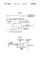
- FIG. 1is a plan view (not to scale) of a memory element in accordance with the present invention
- FIG. 2is a diagrammatic representation of a circuit used in testing a memory element made in accordance with the invention
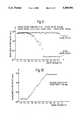
- FIG. 3is a graphical representation of the change in resistance during the forming process
- FIGS. 4 and 5are graphical representation of the change in resistance of a formed device with changing ERASE voltage:
- FIGS. 6 and 7are graphical representations of the variation of resistance with number of constant voltage ERASE and WRITE pulses applied to a device according to the invention, the constant ERASE pulse being of a greater magnitude in FIG. 7 than in FIG. 6.
- FIG. 8is a graphical representation of the change in resistance of a device according to the invention as WRITE Pulses of increasing magnitude are applied to it;
- FIG. 9is a graphical representation of the change in resistance of a device according to the invention alternatively subjected to an ERASE pulse of constant magnitude and a WRITE Pulse of increasing magnitude;
- FIG. 10is a graphical representation of the change in resistance of a device according to the invention initially in its ON stage and subjected to ERASE pulses of increasing magnitude;
- FIG. 11is a graphical representation of the change in resistance of a device according to the invention which is initially in its ON stage and which is alternatively subjected to ERASE pulses of varying magnitude and WRITE Pulses of constant magnitude;
- FIG. 12is a graphical representation of the change in resistance of a device according to the invention which is initially in the OFF state and which is subjected to WRITE Pulses which increase in magnitude:;
- FIG. 13is a graphical representation of the change in resistance of a device according to the invention subjected to alternatively WRITE and ERASE Pulses, with the ERASE Pulse held constant and the WRITE Pulse increasing in magnitude;
- FIG. 14is a graphical representation of the change in resistance of a device not according to the present invention which is initially in a high resistance state and which is subjected to voltage pulses of increasing magnitude, showing the rapid transition from a very high resistance state to a high resistance state when a critical voltage threshold is exceeded;
- FIG. 15is a graphical representation cf the change in resistance of a device not according to the invention Which is initially in an ON state and is subjected to ERASE voltage pulses of increasing magnitude;
- FIG. 16is a graphical representation of the change in resistance of a device not according to the invention which is initially in the OFF state and which is subjected to WRITE Pulses of increasing magnitude.
- a WRITE pulsecan be considered as one which sets the device to a state corresponding to either binary 0 or 1 while an ERASE pulse can be considered as a pulse which always resets the device to to an opposite state (binary 1 or 0).
- a WRITE pulseis a pulse which tends to reduce the resistance of the device and an ERASE pulse is a pulse which tends to increase it.
- a STORE Pulse which stores analogue information in the device about the magnitude of the voltage applied to itmay be a WRITE or an ERASE pulse.
- a RESET Pulse which turns the device fully ON or OFFmay thus be a WRITE or ERASE pulse provided it is of sufficient magnitude to change the device to the fully ON or OFF state.
- a structurecomprising a glass substrate, chromium first conducting layer, a layer cf hydrogenated amorphous silicon doped with doborane, (B 2 H 6 ), and a top contact layer was fabricated as follows:
- the glass structurewas "Corning 7059” glass ("Corning” is a trademark) of thickness about 0.75 mm and length and width 45 mm and 20 mm respectively.
- a chromium layer of thickness about 150 nmwas deposited on this substrate by standard thermal evaporation of chromium granules from an electrically heated tungsten filament in vacuum and subsequently patterned by conventional photolithography.
- the amorphous siliconwas deposited on this substrate in a single layer by the radio frequency glow discharge decomposition of a mixture of SiN 4 and about 10 4 vppm of B 2 H 6 , obtained by admitting silane gas and a gas mixture of 5 ⁇ doborane in hydrogen to the vacuum system via flow controllers.
- the glass substratewas mounted on a substrate holder contained within a vacuum pumped glass tube enclosure and heated to 310° C. (via a heater element contained within the substrate holder) at a vacuum of less than 10 -6 torr. Nitrogen gas was then admitted to the system to raise the vacuum to 0.1 torr and a gas plasma discharge induced (as defined below) for a period of 4 minutes (power input 8W).
- the dischargewas then extinguished, the N 2 flow stopped and the system pumped below 10 -6 torr.
- the silane/doborane/hydrogen gaseswere then admitted to the chamber, flow conditions being set to achieve both silane/doborane ratio and a constant gas pressure of 0.1 torr, resulting from the balance of incoming gas flow and outgoing pumped gas.
- a gas plasma dischargewas then induced using a radio frequency generator running at 40MHz and capacitively coupled to the gas via the substrate holder and tow external secondary electrodes 6cm away from the substrate. Power input from the generator was 8 watts corresponding to a power density of 20mW/cm 2 at the substrate.
- the RF dischargewas maintained for 5.5 minutes and then extinguished.
- the resulting samplewas cooled under vacuum and removed from the deposition system.
- the a-Si film resulting from thiswas measured to be 900 Angstrom thick ⁇ 50 Angstrom (90 nm ⁇ 5nm).
- the level of conductivity due to the B 2 H 6 dopingwas measured to be between 10 -3 and 10 -2 (ohms.cm) -1 in separate experiments using the same deposition conditions, corresponding to p + a-Si:H.
- the amorphous silicon layerwas then patterned using conventional lithography into a number of discrete elements of dimensions 900 ⁇ 500 micrometers, overlying regions of the chromium first conducting layer.
- An insulator layerwas then provided over all but a very small area of the amorphous silicon, (itself overlying the first conducting layer), in order to define the area to be contacted by the final metal. This was done using a 1.2 micrometers thick insulator of photoresist (Shipley Microposit S1818) which was patterned, baked and cured at 200° to delineate the device area of 10 -6 cm 2 .
- FIG. 1shows a plan view of the device made by this technique
- the finished samplewas designated 779/1.
- the electrical characteristics of an individual element on this samplewere measured as follows.
- the elementwas contacted using two electrical probe needles contacting the top and bottom metallisations. These probes were connected to a switching network, such that with the switch in either one of two positions one probe was connected to the pulse generator and the other probe was connected to one side of a resistor (R S ) and the input to an oscillioscope, the other side of the resistor being connected to earth. With the switch in the opposite position, these connections were reversed.
- the circuitis shown in FIG. 2.
- application of a voltage pulse to the deviceusing the pulse generator, induced a current in both the device and resistor R S , thereby inducing a voltage proportional to this current at the oscillioscope .input. Measurement of this voltage allowed calculation of the device resistance.
- R Sneeds to be sufficiently low to permit most of the applied voltage to appear across the device, yet large enough to give a detectable signal on the oscillioscope.
- R S valuesof from 1M ohms (for forming an initial informed measurement) and 100 ohms (for switching measurement) were used.
- a positive pulse(100 nsec, 3.4V) was first applied to the element first contact (Cr), resulting in an ON state of 2 ⁇ 10 3 ohms; (this is defined as a WRITE pulse).
- An opposite polarity pulse, positive to the top contact (V),(defined as an ERASE pulse), was then applied at successively higher voltages and the element resistance determined after each.
- FIG. 4It can be seen that at a threshold voltage of about 1.6V, the element resistance is gradually increased with each successively higher voltage until, at about 3.0V, a final resistance state of about 4 ⁇ 10 5 ohms is achieved. It should be noted that all the states attained were non-volatile and stable, i.e. in the absence of any attempt to switch the element (e.g. with zero bias or when disconnected), it retained the conductivity state it had last been set to.
- the element resistanceis primarily a function of applied voltage pulse, not of the number of pulses applied as might be deduced from FIG. 4.
- the elementcan controllably be set on an intermediate resistance between an upper and lower bound.
- the elementwas first set to its high resistivity state (8 ⁇ 10 5 ohms) using an ERASE pulse of +3.4V, 100 nsec (applied to top contact (V)).
- a series of WRITE Pulses of 100 nsec durationwere then applied to the element, starting at 1.2. V and incrementing each successive pulse of 0.05V up to 3.3V.
- the element resistancewas measured after each pulse and the results are shown in FIG. 8. As before, intermediate resistance states are obtained for WRITE pulses between a lower threshold voltage and upper threshold voltage (of about 1.6V and 2.7V respectively), though there is far more scatter in the curve than for the case of incremental ERASE (FIG. 4).
- Example 1A sample was made as in Example 1, but with a first metal layer of 50 nm vanadium deposited by thermal evaporation as defined in Example 1. a-Si deposition was done simultaneously with Example 1 and the finished sample (V-p - -V) designated 779/2.
- FIG. 10shows the results of experiment (a), (in which after initial WRITE Pulse (100 nsec, 3.4V to bottom contact), a sequence of 100 nsec ERASE pulses are applied from 1.2V to 3.2V in 0.05V steps).
- FIG. 11shows the results of an experiment (b) (a sequence of alternating 3.4V, 100 nsec WRITE Pulses, each followed by an incremented 100 nsec ERASE pulse from experiment.
- FIG. 12shows the results from experiment (c) (initial ERASE pulse of 3.4 kV, 100 nsec, followed by incrementally increasing WRITE pulses of 100 nsec, 1.2V to 3.4V in 0.05V steps).
- FIG. 13shows the results from experiment (d) (alternative 3.4.V, 100 nsec ERASE Pulses followed by 100 nsec WRITE Pulses, incremented from 1.2V to 3.4V in 0.05V steps).
- Example 2A sample was made as in Example 1, but with a final (top) metal layer of about 50 nm Cr, deposited as for the first bottom metal layer. a-Si deposition was done simultaneously with Example 1 and the finished sample (Cr-p + -Cr) designated 779/3.
- Example 2An element of this sample was tested as in Example 1. Initially a series of 250 nsec positive voltage pulses were applied to the top contact, each successive pulse being higher than the last, until the "forming" event took place. The results of this test are shown in FIG. 14; note that resistance changes take place over a much narrower voltage range than in the corresponding test on examples 1 and 2 (FIG. 3).
- FIG. 15shows the results for method (1)
- FIG. 16the results for method (c). Note that although similar resistance limits are seen in this element compared to those of examples 1 and 2, (i.e. from 2 ⁇ 10 3 ohms to 3.5 ⁇ 10 5 ), and some intermediate states do exist, the voltage range over which these intermediate states can be obtained is far narrower than the range of examples 1 and 2. This makes it extremely difficult to obtain reliable programming of the intermediate states and the element is only suitable for digital use, (i.e. from the 2 ⁇ 10 3 ) ohms state to the 3.5 ⁇ 10 5 ohms state), and is corresponding classified as a digital device.
- a number of sampleswere made essentially as for example 1, (i.e. glass Cr first conducting layer, circa 900 Angstrom a-Si:H doped with H 2 H 6 ), but a number of different top contact metal films were deposited in place of the V film of example 1.
- Each samplewas then tested as in example 1 and the range of switching voltages over which intermediate states could be obtained was determined. Devices were accordingly classified as digital (switching ranges ⁇ 0.5V ) or analogue (switching range ⁇ 0.5V); preferred analogue devices were defined as those exhibiting a switching range of 2.0V or more. Table 1 lists the results of this test.
Landscapes
- Engineering & Computer Science (AREA)
- Manufacturing & Machinery (AREA)
- Semiconductor Memories (AREA)
- Mechanical Treatment Of Semiconductor (AREA)
- Bipolar Transistors (AREA)
- Noodles (AREA)
- Non-Volatile Memory (AREA)
- Secondary Cells (AREA)
- Crystals, And After-Treatments Of Crystals (AREA)
- Table Devices Or Equipment (AREA)
- Design And Manufacture Of Integrated Circuits (AREA)
Abstract
Description
This is a continuation of application Ser. No. 07/761,907, filed Sep. 25, 1991, now abandoned.
The present invention relates to novel semiconductor devices capable of being set and reset to a plurality of different conductance states.
Most semiconductor devices are used in binary digital systems in which the device is in one of two states (e.g. a high and low resistance) which can be used to represent binary 0 and binary 1. However there is increasing interest in devices which can be in more than two states. Devices which can be set and reset into more than two conductance states (as opposed to the two states of digital devices) are potentially useful in structures known as neural networks which attempt to reproduce some of the arrangements of the human brain.
According to the present invention there is provided an analogue memory device capable of being set and reset into a resistance which is a measure of a voltage applied to it and which comprises
(a) a first conducting layer;
(b) a thin layer of a doped amorphous silicon above the first conducting layer;
(c) a metal top contact deposited on s aid amorphous silicon layer, the metal being one of V, Co, Ni, Pd, Fe or Mn; and
(d) the thin layer having been subjected to a voltage sufficiently high to convert it into an analogue memory device.
The nature of the first conducting layer is not critical as long as it is possible to grow the required amorphous silicon (a-Si) layer upon it. Examples of suitable materials are Cr or V. Examples of unsuitable materials are gold (which diffuses into the a-Si layer and mercury (which is liquid). The first conducting layer need not extend on the whole area of the amorphous silicon overlying it. Reference to the amorphous silicon layer being above the first conducting layer do not carry any implication about the orientation of the device in use but are intended to indicate only that the silicon is deposited after the first conducting layer.
The amorphous silicon must be dopable i.e. it must be possible to increase its conductivity by incorporating elements having higher or lower valency than silicon. Some techniques of depositing amorphous silicon may give silicon containing high levels of defects which cannot be doped e.g. Argon sputtering of a Si target in the absence silicon are well known to those skilled in the art. Thus low pressure plasma decomposition of silanes (optionally in the presence of hydrogen or fluorine onto a heated substrate may be used).
The deposition of amorphous silicon is discussed in W E Spear and P G LeComber, Topics in Applied Physics, Vol 55, (The Physics of Hydrogenated Amorphous silicon I) 1984 pages 65-71.
The amorphous silicon is doped. The silicon may be doped to produce n-type conductivity by incorporating an element with a higher valency e.g. P, or may be doped to give p-type conductivity as a result of introducing element of lower valency e.g.B.
The amorphous silicon is, preferably, doped so as to have a conductivity in the bulk state of at least 10-6 (ohms cm)-1. The degree of doping is more preferably such as to correspond to p+ or n+ -silicon e.g. to conductivities greater than 10-4 (ohms cm)-1.
Methods of producing doped amorphous silicon are well known to those skilled in the art. The silicon is preferably p+ silicon.
The thickness of the doped amorphous silicon is preferably in the range 200 Angstroms to 0.35 micrometers (20 to 350nm). The amorphous silicon layer may be pure hydrogenated amorphous silicon (apart from any doping) or may be a hydrogenated silicon alloy, e.g. a silicon germanium alloy.
The dopable silicon or silicon alloy may contain fluorine.
The identity of the top contact is important in obtaining analogue memory properties. In the production of semiconductor devices semiconductor layers are often deposited on a conducting substrate and a metal layer is deposited in a final step after the semiconductor layers have been deposited. This metal layer is the top contact of the device. The metal layer may, of course, be covered by encapsulating layers or by an additional metal layer which is used to obtain better contact with the metal layer in direct contact with he silicon. It is common in the semiconductor industry to stack devices one above the other in integrated circuits. It may be possible to stack other semiconducting and conducting layers above the device of the present invention to form other devices within a single integrated circuit.
Preferably the top contact metal is V, Co, Ni or Pd.
The metal may be deposited for example by thermal evaporation or by sputtering.
The thickness of the metal is not believed to be critical. Those skilled in the art will understand that the normal-requirements for producing metal contacts will imply certain limits. Thus there may be problems of electrical continuity if the layer is too thin and there may be problems of mechanical strain if the layer is too thick. The thickness of the layer may for example be 50 Angstroms (5nm) to 50 micrometers, preferably 100 Angstroms (10 nm) to 1 micrometer, more preferably 20 nm to 50 nm.
The device is a two terminal device. It is preferably in the form of a layer of amorphous silicon of a single conductivity type deposited on a conductive substrate as bottom contact. The nature of the bottom contact is not believed to be critical. Thus the bottom contact may be Cr even though Cr does not give useful analogue memory properties when used as a top contact.
The top contact is preferably in contact only with a relatively small area of the amorphous silicon layer for each device, as this allows large numbers of devices to be fabricated in a small area, so giving compact integrated circuits. A typical contact has an area of 10-6 cm2. This can be readily achieved by the well-known process of photolithography.
A step of applying a voltage across the device to change the electrical characteristics is required. Such permanent electrical modification of semiconductor devices is often known as "forming" to those skilled in the art. The device as initially produced, before being subjected to the "forming" step has a relatively high resistance. Thus the resistance may be of the order of 109 ohms.
For the preferred device containing only silicon of a single conductivity type references to forward or backward bias are meaningless and in principle it does not matter whether the top contact is positive or negative in relation to the bottom contact during the forming process.
Preferably, however, the top contact is positive in relation to the bottom contact during the forming process.
The forming step is preferably divided into two stages, a "soft" forming step and a "hard" forming step. The "hard" forming step is a step which converts the a-Si structure into a device having the desired and analogue memory properties. It is possible to "hard" form the device in a single step by applying a voltage which is sufficiently large to convert the structure to a memory device having a resistance less than the full OFF state. However, as indicated above, it is preferred to carry out a "soft" forming step initially. This involves applying a voltage which is sufficiently high (for example 13-14 volts) to permanently change the characteristics of the device and to reduce its resistance (for example, by two orders of magnitude) without transforming it to a device having analogue memory properties. The final "hard" forming step may be carried out by applying a further, slightly higher voltage (for example the order of 1 to 2 volts above the soft-forming voltage). Thus the initial "soft" forming events can be used to judge the voltage required for hard forming, resulting in a more controlled process. After "hard" forming the resistance of the analogue memory device will be lower than that of the "soft" formed structure (for example an order of magnitude or more lower). It will then be below the maximum resistance (the fully OFF stage) to which it can be reset in use.
The magnitude cf the forming voltage depends on the thickness of the amorphous silicon layer. It is preferably in therange 6 to 16 volts.
It is necessary to control the energy applied to the structure, as excessive energy can produce damage which prevents a satisfactory device being produced. The energy can be controlled by placing a resistance in circuit and by using short voltage pulses. Example of pulse lengths which may be used are 50 ns to 1 microsecond.
The devices of the present invention can be set and reset to a resistance which is a measure of an applied voltage. By "set" we mean that the device will retain this resistance even when the voltage which caused it to take this resistance has been removed. By "reset" we mean that the resistance can be changed to a new set value and is not permanently fixed in the original set value. The devices of the present invention are thus distinguished from threshold devices which only retain a given stage as long as a holding voltage is applied to them. They are different from the known binary memory devices in which the resistance may depend on the applied voltage but all voltages below a certain value correspond to one resistance and all voltages above another value correspond to another resistance. The devices of the present invention do not show analogue memory properties over the whole range of voltages which can be applied to them. It will be appreciated that a device which shows analogue memory properties over a voltage range of say 10 millivolts is not in practice a useful device. It is preferred therefore to select metal contacts which give analogue memory properties over a voltage range of at least 0.5V, and preferably over at least one V, more preferably over more than 2V.
The device after "forming" will normally be in a resistance state between the ON and OFF states. By applying a positive voltage pulse of sufficient voltage to the top contact, the device can be set into its highest (or OFF) resistance state. It can then be placed in a lower resistance state by making the bottom contact positive with respect to the top contact. If the voltage is sufficiently high the device will be switched to its minimum resistance (the fully ON state). Lesser voltages, providing they are within the appropriate voltage range will switch the device to an intermediate resistance which is related to the voltage applied.
An alternative method of setting the device is to apply a sufficient voltage to switch the "formed" device back to the fully ON state. It may then be switched to a lower resistance intermediate between the fully OFF and the full ON states, by the application of a positive voltage to the top contact.
The switching in the "formed" analogue memory device is preferably carried out with short voltage pulses for example pulses of length in therange 10 ns to 500 nsec.
The invention will now be described with reference to the accompanying drawings in which:
FIG. 1 is a plan view (not to scale) of a memory element in accordance with the present invention;
FIG. 2 is a diagrammatic representation of a circuit used in testing a memory element made in accordance with the invention;
FIG. 3 is a graphical representation of the change in resistance during the forming process;
FIGS. 4 and 5 are graphical representation of the change in resistance of a formed device with changing ERASE voltage:
FIGS. 6 and 7 are graphical representations of the variation of resistance with number of constant voltage ERASE and WRITE pulses applied to a device according to the invention, the constant ERASE pulse being of a greater magnitude in FIG. 7 than in FIG. 6.
FIG. 8 is a graphical representation of the change in resistance of a device according to the invention as WRITE Pulses of increasing magnitude are applied to it;
FIG. 9 is a graphical representation of the change in resistance of a device according to the invention alternatively subjected to an ERASE pulse of constant magnitude and a WRITE Pulse of increasing magnitude;
FIG. 10 is a graphical representation of the change in resistance of a device according to the invention initially in its ON stage and subjected to ERASE pulses of increasing magnitude;
FIG. 11 is a graphical representation of the change in resistance of a device according to the invention which is initially in its ON stage and which is alternatively subjected to ERASE pulses of varying magnitude and WRITE Pulses of constant magnitude;
FIG. 12 is a graphical representation of the change in resistance of a device according to the invention which is initially in the OFF state and which is subjected to WRITE Pulses which increase in magnitude:;
FIG. 13 is a graphical representation of the change in resistance of a device according to the invention subjected to alternatively WRITE and ERASE Pulses, with the ERASE Pulse held constant and the WRITE Pulse increasing in magnitude;
FIG. 14 is a graphical representation of the change in resistance of a device not according to the present invention which is initially in a high resistance state and which is subjected to voltage pulses of increasing magnitude, showing the rapid transition from a very high resistance state to a high resistance state when a critical voltage threshold is exceeded;
FIG. 15 is a graphical representation cf the change in resistance of a device not according to the invention Which is initially in an ON state and is subjected to ERASE voltage pulses of increasing magnitude; and
FIG. 16 is a graphical representation of the change in resistance of a device not according to the invention which is initially in the OFF state and which is subjected to WRITE Pulses of increasing magnitude.
It should be noted that in a digital device a WRITE pulse can be considered as one which sets the device to a state corresponding to either binary 0 or 1 while an ERASE pulse can be considered as a pulse which always resets the device to to an opposite state (binary 1 or 0). In the present specification a WRITE pulse is a pulse which tends to reduce the resistance of the device and an ERASE pulse is a pulse which tends to increase it. Thus a STORE Pulse which stores analogue information in the device about the magnitude of the voltage applied to it may be a WRITE or an ERASE pulse. A RESET Pulse which turns the device fully ON or OFF may thus be a WRITE or ERASE pulse provided it is of sufficient magnitude to change the device to the fully ON or OFF state.
A structure comprising a glass substrate, chromium first conducting layer, a layer cf hydrogenated amorphous silicon doped with doborane, (B2 H6), and a top contact layer was fabricated as follows:
The glass structure was "Corning 7059" glass ("Corning" is a trademark) of thickness about 0.75 mm and length and width 45 mm and 20 mm respectively. A chromium layer of thickness about 150 nm was deposited on this substrate by standard thermal evaporation of chromium granules from an electrically heated tungsten filament in vacuum and subsequently patterned by conventional photolithography.
The amorphous silicon was deposited on this substrate in a single layer by the radio frequency glow discharge decomposition of a mixture of SiN4 and about 104 vppm of B2 H6, obtained by admitting silane gas and a gas mixture of 5Δ doborane in hydrogen to the vacuum system via flow controllers. The glass substrate was mounted on a substrate holder contained within a vacuum pumped glass tube enclosure and heated to 310° C. (via a heater element contained within the substrate holder) at a vacuum of less than 10-6 torr. Nitrogen gas was then admitted to the system to raise the vacuum to 0.1 torr and a gas plasma discharge induced (as defined below) for a period of 4 minutes (power input 8W). The discharge was then extinguished, the N2 flow stopped and the system pumped below 10-6 torr. The silane/doborane/hydrogen gases were then admitted to the chamber, flow conditions being set to achieve both silane/doborane ratio and a constant gas pressure of 0.1 torr, resulting from the balance of incoming gas flow and outgoing pumped gas. A gas plasma discharge was then induced using a radio frequency generator running at 40MHz and capacitively coupled to the gas via the substrate holder and tow external secondary electrodes 6cm away from the substrate. Power input from the generator was 8 watts corresponding to a power density of 20mW/cm2 at the substrate. The RF discharge was maintained for 5.5 minutes and then extinguished. The resulting sample was cooled under vacuum and removed from the deposition system. The a-Si film resulting from this was measured to be 900 Angstrom thick ±50 Angstrom (90 nm ±5nm). The level of conductivity due to the B2 H6 doping was measured to be between 10-3 and 10-2 (ohms.cm)-1 in separate experiments using the same deposition conditions, corresponding to p+ a-Si:H.
The amorphous silicon layer was then patterned using conventional lithography into a number of discrete elements of dimensions 900×500 micrometers, overlying regions of the chromium first conducting layer. An insulator layer was then provided over all but a very small area of the amorphous silicon, (itself overlying the first conducting layer), in order to define the area to be contacted by the final metal. This was done using a 1.2 micrometers thick insulator of photoresist (Shipley Microposit S1818) which was patterned, baked and cured at 200° to delineate the device area of 10-6 cm2.
A top contact of vanadium was deposited over the device by the thermal evaporation of vanadium foil from an electrically heated tungsten filament in vacuum, to a thickness of 60 nm. This was patterned using conventional lithography techniques to provide individual contacts to each of the previously defined a-Si elements; this patterning also provided probing pads of the vanadium to one side of the devices, isolated from both chromium first layer and the a-Si layer except in the previously defined contact area. FIG. 1 shows a plan view of the device made by this technique
The finished sample was designated 779/1. The electrical characteristics of an individual element on this sample were measured as follows.
The element was contacted using two electrical probe needles contacting the top and bottom metallisations. These probes were connected to a switching network, such that with the switch in either one of two positions one probe was connected to the pulse generator and the other probe was connected to one side of a resistor (RS) and the input to an oscillioscope, the other side of the resistor being connected to earth. With the switch in the opposite position, these connections were reversed. The circuit is shown in FIG. 2. Hence, application of a voltage pulse to the device, using the pulse generator, induced a current in both the device and resistor RS, thereby inducing a voltage proportional to this current at the oscillioscope .input. Measurement of this voltage allowed calculation of the device resistance. It will be appreciated that the value of RS needs to be sufficiently low to permit most of the applied voltage to appear across the device, yet large enough to give a detectable signal on the oscillioscope. Typically, RS values of from 1M ohms (for forming an initial informed measurement) and 100 ohms (for switching measurement) were used.
In order to measure device resistance, a low voltage of 0.5V was output from the pulse generator as continuous DC level; pulses for forming and switching were superimposed on this. Initially, the resistance of the element as made above was measured to be greater than 108 ohms. The element was then subjected to a procedure in which its electrical properties were modified by the application of voltage pulses. A succession of 250 nsec. voltage pulses of progressively increasing voltage were applied across the a-Si film, with top (V) contact being at positive potential with respect to the first (Cr) contact. After each pulse the element resistance was determined as described above. FIG. 3curve 1 shows the device resistance against previous voltage pulse as successive pulses are applied. (Note that the device resistance is stable until a further voltage pulse is applied and never returns to its original value once modified). At a voltage of between 13.5 and 14 volts, the resistance fell abruptly to a value of 7×10⁵ ohms, within the expected switching range of this element. It was then possible to obtain an even lower resistance in the device using far smaller negative voltage pulses (3.4V, 100 nsec), testifying to the permanent and dramatic change in device properties of the formed element that were then studied.
A positive pulse (100 nsec, 3.4V) was first applied to the element first contact (Cr), resulting in an ON state of 2×10³ ohms; (this is defined as a WRITE pulse). An opposite polarity pulse, positive to the top contact (V), (defined as an ERASE pulse), was then applied at successively higher voltages and the element resistance determined after each. The results of this test are shown in FIG. 4. It can be seen that at a threshold voltage of about 1.6V, the element resistance is gradually increased with each successively higher voltage until, at about 3.0V, a final resistance state of about 4×10⁵ ohms is achieved. It should be noted that all the states attained were non-volatile and stable, i.e. in the absence of any attempt to switch the element (e.g. with zero bias or when disconnected), it retained the conductivity state it had last been set to.
In order to fully demonstrate the voltage programmability of the device an alternative method of use was tested. In this example a positive, 100 nsec WRITE pulse of 3.4V was applied to the element first or bottom contact (Cr) to set the element to its low resistance state and the resistance measured (2×10³) ohms; a positive, 100 nsec ERASE Pulse of, initially 1.2V was then applied to the element top contact (V) and the device resistance remeasured. This procedure was repeated with the ERASE pulse being increased by 0.05V on each successive occasion. The results of this test are shown in FIG. 5; as expected, the application of the WRITE Pulse resulted in a constant resistance value whilst increasing ERASE Pulse amplitude gave rise to a range of resistance values between 2×10³ ohms and 4×10⁵ ohms. This demonstrates that, between the upper and lower switching thresholds, the element resistance is primarily a function of applied voltage pulse, not of the number of pulses applied as might be deduced from FIG. 4. Thus the element can controllably be set on an intermediate resistance between an upper and lower bound. The reproducibility of the switching to these intermediate resistance states was tested by repeatedly applying fixed ERASE and WRITE Pulses of 100 nsec, 3.4 v and ERASE Pulses of 100 nsec 2.1V and 100 nsec 2.4V are shown in FIGS. 6 and 7 respectively. Over the duration of the test, the application of fixed pulses results in constant resistance values. (The scatter in the value after ERASE is to be expected due to small fluctuations in the value of applied voltage from the equipment; it is because of this that a wide voltage threshold range is desirable, in order to provide as many usable intermediate states as possible).
A further method of using the element was tested. The element was first set to its high resistivity state (8×10⁵ ohms) using an ERASE pulse of +3.4V, 100 nsec (applied to top contact (V)). A series of WRITE Pulses of 100 nsec duration were then applied to the element, starting at 1.2. V and incrementing each successive pulse of 0.05V up to 3.3V. The element resistance was measured after each pulse and the results are shown in FIG. 8. As before, intermediate resistance states are obtained for WRITE pulses between a lower threshold voltage and upper threshold voltage (of about 1.6V and 2.7V respectively), though there is far more scatter in the curve than for the case of incremental ERASE (FIG. 4).
A further test was made in which a constant ERASE pulse of 3.4V, 100 nsec was applied to the element to reset it to its highest resistance state, followed by a WRITE Pulse of 100 nsec, voltage being incremented by 0.05V from 1.2V to 3.4V on successive repeats. Resistance was measured after each pulse and the results are shown in FIG. 9; as was the case for constant WRITE, incremental ERASE (FIG. 5), the intermediate resistance states are seen to be primarily a function of previously applied voltage pulse.
A sample was made as in Example 1, but with a first metal layer of 50 nm vanadium deposited by thermal evaporation as defined in Example 1. a-Si deposition was done simultaneously with Example 1 and the finished sample (V-p- -V) designated 779/2.
An element of this sample was tested as in Example 1. Initially a series of 250 nsec positive voltage pulses were applied to the top contact, each successive pulse being of higher voltage than the last; element resistance was measured after each pulse. The test was stopped once the "forming" event was seen to take place (i.e. an abrupt change in resistance to 6×10⁵ ohms). The results of this test are shown incurve 2 in FIG. 3.
A further 4 experiments ((a)-(d) defined in Example 1) were then applied to the element to determine the dependence of the element resistance on previously applied voltage pulse.
FIG. 10 shows the results of experiment (a), (in which after initial WRITE Pulse (100 nsec, 3.4V to bottom contact), a sequence of 100 nsec ERASE pulses are applied from 1.2V to 3.2V in 0.05V steps).
FIG. 11 shows the results of an experiment (b) (a sequence of alternating 3.4V, 100 nsec WRITE Pulses, each followed by an incremented 100 nsec ERASE pulse from experiment.
FIG. 12 shows the results from experiment (c) (initial ERASE pulse of 3.4 kV, 100 nsec, followed by incrementally increasing WRITE pulses of 100 nsec, 1.2V to 3.4V in 0.05V steps).
FIG. 13 shows the results from experiment (d) (alternative 3.4.V, 100 nsec ERASE Pulses followed by 100 nsec WRITE Pulses, incremented from 1.2V to 3.4V in 0.05V steps).
These tests show that the V-p+ -V sample behaves similarly to the V-p+ -Cr sample of Example 1; most importantly, there is no indication that replacing the first Cr metal layer with V induces further (opposite polarity) switching in the structure.
A sample was made as in Example 1, but with a final (top) metal layer of about 50 nm Cr, deposited as for the first bottom metal layer. a-Si deposition was done simultaneously with Example 1 and the finished sample (Cr-p+ -Cr) designated 779/3.
An element of this sample was tested as in Example 1. Initially a series of 250 nsec positive voltage pulses were applied to the top contact, each successive pulse being higher than the last, until the "forming" event took place. The results of this test are shown in FIG. 14; note that resistance changes take place over a much narrower voltage range than in the corresponding test on examples 1 and 2 (FIG. 3).
After "forming" , the element was tested using method (a) and method (c) previously defined to determine the presence of intermediate resistance states.
FIG. 15 shows the results for method (1)
FIG. 16 the results for method (c). Note that although similar resistance limits are seen in this element compared to those of examples 1 and 2, (i.e. from 2×10³ ohms to 3.5×10⁵), and some intermediate states do exist, the voltage range over which these intermediate states can be obtained is far narrower than the range of examples 1 and 2. This makes it extremely difficult to obtain reliable programming of the intermediate states and the element is only suitable for digital use, (i.e. from the 2×10³) ohms state to the 3.5×10⁵ ohms state), and is corresponding classified as a digital device.
A number of samples were made essentially as for example 1, (i.e. glass Cr first conducting layer, circa 900 Angstrom a-Si:H doped with H2 H6), but a number of different top contact metal films were deposited in place of the V film of example 1. Each sample was then tested as in example 1 and the range of switching voltages over which intermediate states could be obtained was determined. Devices were accordingly classified as digital (switching ranges <0.5V ) or analogue (switching range <0.5V); preferred analogue devices were defined as those exhibiting a switching range of 2.0V or more. Table 1 lists the results of this test.
TABLE 1 ______________________________________ Survey of p.sup.+ -switching with different top metals all the bottom contacts are chromium. T.E. = thermal evaporation of top metal. S = sputtered top metal. Exam- ple Metal or top Meth- Switching Switching test contact od Type Range Comments ______________________________________ B Cr T.E. Digital <0.5 V Intermediate states exist 3 V T.E. Analogue >2.0 V Preferred 4 Fe T.E. Analogue 0.5-1.0 V -- 5 Ni T.E. Analogue 2.0 V Preferred C Au T.E. No -- -- switching D Cu T.E. No -- -- switching 6 Co T.E. Analogue >2.0 V Preferred E Ti T.E. Unstable -- -- F Mo S Unstable -- -- 7 Pd S Analogue 2.0 V Preferred G W S Digital -- -- 8 Mn -- Analogue 0.5-1.0 V -- H Ag -- Digital <0.5 V No intermediate states obtained I Al -- No -- -- switching ______________________________________
Claims (11)
1. An analog memory device capable of being set and reset to a resistance value over a continuous range of resistance values which is a measure of a voltage applied to it over a corresponding range of voltage values, said analog memory device comprising:
a first conducting layer (a);
a single thin layer (b) in direct electrical contact with layer (a);
a metal top contact (c) in electrical contact with layer (b) without interposition of an intermediate conductive layer, the metal being one of V, Co, Ni, Pd, Fe or Mn;
wherein layer (b) exhibits said range of resistance values and is located between layer (a) and layer (c), said layer (b) being formed by one of (i) pure or doped amorphous silicon, (ii) pure or doped amorphous hydrogenated silicon or (iii) a hydrogenated silicon alloy; and
wherein layer (b) has been subjected to a voltage sufficiently high to convert it into an analog memory device exhibiting said range of settable resistance values.
2. An analog memory device as in claim 1, wherein layer (b) is formed of doped amorphous silicon.
3. An analog memory device as in claim 1, wherein the metal of the top contact is V, Co, Ni or Pd.
4. A method of making an analog memory device capable of being set and rest into a resistance over a continuous range of more than two resistance values which is a measure of a voltage applied to it over a corresponding range of voltage values, said method comprising the steps of:
(i) depositing a first conducting layer (a) directly on an insulating substrate;
(ii) depositing a thin layer (b) of one of (i) pure or doped amorphous silicon, (ii) pure or doped amorphous hydrogenated silicon or (iii) a hydrogenated silicon alloy on layer (a);
(iii) depositing a contact layer (c) of V, Co, Ni, Pd, Fe or Mn on layer (b) without interposition of an intermediate conductive layer;
(iv) applying a first forming voltage to the device, said voltage being sufficient to permanently reduce the resistance of the device; and
(v) applying a second voltage to further reduce the resistance of the element.
5. A method as in claim 4 wherein the first forming voltage is 13-14 volts, the second forming voltage is 1-2 volts higher than the first forming voltage and layer (b) is 20-350 nm thick.
6. A neural network structure including a plurality of analog memory devices as in claim 1 wherein said neural network structure comprises an insulating substrate having deposited thereon a plurality of said analog memory devices wherein each layer (a) is in contact with said insulating substrate.
7. An analog memory device for use in a neural network as a variable resistance element that can be set and reset to any resistance within a continuous range of resistance values as a function of voltage applied thereto, said analog memory device comprising:
a single layer of amorphous silicon grown directly over a first electrical contact layer;
a second electrical contact layer of V, Co, Ni, Pd, Fe or Mn grown over said single layer of amorphous silicon without interposition of an intermediate conductive layer;
said single layer of amorphous silicon being altered after growth thereof by application of a forming voltage sufficient to convert this layer into a variable resistance element that can thereafter be reliably set and reset to retain any resistance within a continuous range of resistance values as a function of voltage applied thereto until subsequently again set or reset to a different value of resistance.
8. An analog memory device as in claim 7 wherein said amorphous silicon, except for dopant, is hydrogenated amorphous silicon.
9. An analog memory device as in claim 7 wherein said amorphous silicon is a hydrogenated silicon alloy.
10. An analog memory device as in claim 7 wherein said amorphous silicon is a silicon germanium alloy.
11. An analog memory device as in claim 7 wherein said amorphous silicon contains fluorine.
Priority Applications (1)
| Application Number | Priority Date | Filing Date | Title |
|---|---|---|---|
| US08/194,628US5360981A (en) | 1989-05-11 | 1990-05-04 | Amorphous silicon memory |
Applications Claiming Priority (5)
| Application Number | Priority Date | Filing Date | Title |
|---|---|---|---|
| GB898910854AGB8910854D0 (en) | 1989-05-11 | 1989-05-11 | Semiconductor device |
| GB8910854 | 1989-05-11 | ||
| PCT/GB1990/000692WO1990013921A1 (en) | 1989-05-11 | 1990-05-04 | Semiconductor device |
| US08/194,628US5360981A (en) | 1989-05-11 | 1990-05-04 | Amorphous silicon memory |
| US76190791A | 1991-09-25 | 1991-09-25 |
Related Parent Applications (1)
| Application Number | Title | Priority Date | Filing Date |
|---|---|---|---|
| US76190791AContinuation | 1989-05-11 | 1991-09-25 |
Publications (1)
| Publication Number | Publication Date |
|---|---|
| US5360981Atrue US5360981A (en) | 1994-11-01 |
Family
ID=10656585
Family Applications (1)
| Application Number | Title | Priority Date | Filing Date |
|---|---|---|---|
| US08/194,628Expired - LifetimeUS5360981A (en) | 1989-05-11 | 1990-05-04 | Amorphous silicon memory |
Country Status (10)
| Country | Link |
|---|---|
| US (1) | US5360981A (en) |
| EP (1) | EP0471737B1 (en) |
| JP (1) | JPH0758813B2 (en) |
| AT (1) | ATE115773T1 (en) |
| AU (1) | AU628562B2 (en) |
| CA (1) | CA2051112C (en) |
| DE (1) | DE69015177T2 (en) |
| GB (1) | GB8910854D0 (en) |
| HK (1) | HK138296A (en) |
| WO (1) | WO1990013921A1 (en) |
Cited By (159)
| Publication number | Priority date | Publication date | Assignee | Title |
|---|---|---|---|---|
| US5787042A (en)* | 1997-03-18 | 1998-07-28 | Micron Technology, Inc. | Method and apparatus for reading out a programmable resistor memory |
| US20030045054A1 (en)* | 2001-08-29 | 2003-03-06 | Campbell Kristy A. | Method of forming non-volatile resistance variable devices, method of forming a programmable memory cell of memory circuitry, and a non-volatile resistance variable device |
| US20030068861A1 (en)* | 2001-08-30 | 2003-04-10 | Jiutao Li | Integrated circuit device and fabrication using metal-doped chalcogenide materials |
| US20030095426A1 (en)* | 2001-11-20 | 2003-05-22 | Glen Hush | Complementary bit PCRAM sense amplifier and method of operation |
| US20030185036A1 (en)* | 2002-03-28 | 2003-10-02 | Micron Technology, Inc. | Method for programming a memory cell |
| US6638820B2 (en) | 2001-02-08 | 2003-10-28 | Micron Technology, Inc. | Method of forming chalcogenide comprising devices, method of precluding diffusion of a metal into adjacent chalcogenide material, and chalcogenide comprising devices |
| US20030206433A1 (en)* | 2002-05-03 | 2003-11-06 | Glen Hush | Dual write cycle programmable conductor memory system and method of operation |
| US6646902B2 (en) | 2001-08-30 | 2003-11-11 | Micron Technology, Inc. | Method of retaining memory state in a programmable conductor RAM |
| US6653193B2 (en) | 2000-12-08 | 2003-11-25 | Micron Technology, Inc. | Resistance variable device |
| US6660136B2 (en) | 2002-03-27 | 2003-12-09 | Micron Technology, Inc. | Method of forming a non-volatile resistance variable device and method of forming a metal layer comprising silver and tungsten |
| US20030228717A1 (en)* | 2002-06-06 | 2003-12-11 | Jiutao Li | Co-sputter deposition of metal-doped chalcogenides |
| US20040038432A1 (en)* | 2002-04-10 | 2004-02-26 | Micron Technology, Inc. | Programmable conductor memory cell structure and method therefor |
| US20040042259A1 (en)* | 2002-08-29 | 2004-03-04 | Campbell Kristy A. | Single polarity programming of a pcram structure |
| US6710423B2 (en) | 2001-03-01 | 2004-03-23 | Micron Technology, Inc. | Chalcogenide comprising device |
| US6734455B2 (en) | 2001-03-15 | 2004-05-11 | Micron Technology, Inc. | Agglomeration elimination for metal sputter deposition of chalcogenides |
| US6737312B2 (en) | 2001-08-27 | 2004-05-18 | Micron Technology, Inc. | Method of fabricating dual PCRAM cells sharing a common electrode |
| US6784018B2 (en) | 2001-08-29 | 2004-08-31 | Micron Technology, Inc. | Method of forming chalcogenide comprising devices and method of forming a programmable memory cell of memory circuitry |
| US6791885B2 (en) | 2002-02-19 | 2004-09-14 | Micron Technology, Inc. | Programmable conductor random access memory and method for sensing same |
| US20040179390A1 (en)* | 2003-03-12 | 2004-09-16 | Campbell Kristy A. | Chalcogenide glass constant current device, and its method of fabrication and operation |
| US6809362B2 (en) | 2002-02-20 | 2004-10-26 | Micron Technology, Inc. | Multiple data state memory cell |
| US6812087B2 (en) | 2002-01-31 | 2004-11-02 | Micron Technology, Inc. | Methods of forming non-volatile resistance variable devices and methods of forming silver selenide comprising structures |
| US6815818B2 (en) | 2001-11-19 | 2004-11-09 | Micron Technology, Inc. | Electrode structure for use in an integrated circuit |
| US6818481B2 (en) | 2001-03-07 | 2004-11-16 | Micron Technology, Inc. | Method to manufacture a buried electrode PCRAM cell |
| US6825135B2 (en) | 2002-06-06 | 2004-11-30 | Micron Technology, Inc. | Elimination of dendrite formation during metal/chalcogenide glass deposition |
| US6831019B1 (en) | 2002-08-29 | 2004-12-14 | Micron Technology, Inc. | Plasma etching methods and methods of forming memory devices comprising a chalcogenide comprising layer received operably proximate conductive electrodes |
| US6847535B2 (en) | 2002-02-20 | 2005-01-25 | Micron Technology, Inc. | Removable programmable conductor memory card and associated read/write device and method of operation |
| US6849868B2 (en) | 2002-03-14 | 2005-02-01 | Micron Technology, Inc. | Methods and apparatus for resistance variable material cells |
| US6855975B2 (en) | 2002-04-10 | 2005-02-15 | Micron Technology, Inc. | Thin film diode integrated with chalcogenide memory cell |
| US6858482B2 (en) | 2002-04-10 | 2005-02-22 | Micron Technology, Inc. | Method of manufacture of programmable switching circuits and memory cells employing a glass layer |
| US6864529B2 (en) | 2001-08-23 | 2005-03-08 | Hewlett-Packard Development Company, L.P. | Thin film transistor memory device |
| US6867114B2 (en) | 2002-08-29 | 2005-03-15 | Micron Technology Inc. | Methods to form a memory cell with metal-rich metal chalcogenide |
| US6867064B2 (en) | 2002-02-15 | 2005-03-15 | Micron Technology, Inc. | Method to alter chalcogenide glass for improved switching characteristics |
| US6873538B2 (en) | 2001-12-20 | 2005-03-29 | Micron Technology, Inc. | Programmable conductor random access memory and a method for writing thereto |
| US6882578B2 (en) | 2002-01-04 | 2005-04-19 | Micron Technology, Inc. | PCRAM rewrite prevention |
| US6891749B2 (en) | 2002-02-20 | 2005-05-10 | Micron Technology, Inc. | Resistance variable ‘on ’ memory |
| US6903361B2 (en) | 2003-09-17 | 2005-06-07 | Micron Technology, Inc. | Non-volatile memory structure |
| US6930909B2 (en) | 2003-06-25 | 2005-08-16 | Micron Technology, Inc. | Memory device and methods of controlling resistance variation and resistance profile drift |
| US6937528B2 (en) | 2002-03-05 | 2005-08-30 | Micron Technology, Inc. | Variable resistance memory and method for sensing same |
| US20050201146A1 (en)* | 2003-07-08 | 2005-09-15 | Moore John T. | Method of refreshing a PCRAM memory device |
| US6951805B2 (en) | 2001-08-01 | 2005-10-04 | Micron Technology, Inc. | Method of forming integrated circuitry, method of forming memory circuitry, and method of forming random access memory circuitry |
| US6955940B2 (en) | 2001-08-29 | 2005-10-18 | Micron Technology, Inc. | Method of forming chalcogenide comprising devices |
| US20050248062A1 (en)* | 2004-05-10 | 2005-11-10 | Alexandr Shkolnik | Process for the production of a three-dimensional object with resolution improvement by "pixel-shift" |
| US20060028895A1 (en)* | 2004-08-09 | 2006-02-09 | Carl Taussig | Silver island anti-fuse |
| US7010644B2 (en) | 2002-08-29 | 2006-03-07 | Micron Technology, Inc. | Software refreshed memory device and method |
| US7015494B2 (en) | 2002-07-10 | 2006-03-21 | Micron Technology, Inc. | Assemblies displaying differential negative resistance |
| US7018863B2 (en) | 2002-08-22 | 2006-03-28 | Micron Technology, Inc. | Method of manufacture of a resistance variable memory cell |
| US7022579B2 (en) | 2003-03-14 | 2006-04-04 | Micron Technology, Inc. | Method for filling via with metal |
| US7050327B2 (en) | 2003-04-10 | 2006-05-23 | Micron Technology, Inc. | Differential negative resistance memory |
| US7049009B2 (en) | 2002-08-29 | 2006-05-23 | Micron Technology, Inc. | Silver selenide film stoichiometry and morphology control in sputter deposition |
| US7061004B2 (en) | 2003-07-21 | 2006-06-13 | Micron Technology, Inc. | Resistance variable memory elements and methods of formation |
| US7071021B2 (en) | 2001-05-11 | 2006-07-04 | Micron Technology, Inc. | PCRAM memory cell and method of making same |
| US7087919B2 (en) | 2002-02-20 | 2006-08-08 | Micron Technology, Inc. | Layered resistance variable memory device and method of fabrication |
| US7098068B2 (en) | 2004-03-10 | 2006-08-29 | Micron Technology, Inc. | Method of forming a chalcogenide material containing device |
| US7151688B2 (en) | 2004-09-01 | 2006-12-19 | Micron Technology, Inc. | Sensing of resistance variable memory devices |
| US7151273B2 (en) | 2002-02-20 | 2006-12-19 | Micron Technology, Inc. | Silver-selenide/chalcogenide glass stack for resistance variable memory |
| US7163837B2 (en) | 2002-08-29 | 2007-01-16 | Micron Technology, Inc. | Method of forming a resistance variable memory element |
| US7190048B2 (en) | 2004-07-19 | 2007-03-13 | Micron Technology, Inc. | Resistance variable memory device and method of fabrication |
| US7209378B2 (en) | 2002-08-08 | 2007-04-24 | Micron Technology, Inc. | Columnar 1T-N memory cell structure |
| US7233520B2 (en) | 2005-07-08 | 2007-06-19 | Micron Technology, Inc. | Process for erasing chalcogenide variable resistance memory bits |
| US7251154B2 (en) | 2005-08-15 | 2007-07-31 | Micron Technology, Inc. | Method and apparatus providing a cross-point memory array using a variable resistance memory cell and capacitance |
| US7269044B2 (en) | 2005-04-22 | 2007-09-11 | Micron Technology, Inc. | Method and apparatus for accessing a memory array |
| US7269079B2 (en) | 2005-05-16 | 2007-09-11 | Micron Technology, Inc. | Power circuits for reducing a number of power supply voltage taps required for sensing a resistive memory |
| US7274034B2 (en) | 2005-08-01 | 2007-09-25 | Micron Technology, Inc. | Resistance variable memory device with sputtered metal-chalcogenide region and method of fabrication |
| US7277313B2 (en) | 2005-08-31 | 2007-10-02 | Micron Technology, Inc. | Resistance variable memory element with threshold device and method of forming the same |
| US7294527B2 (en) | 2002-08-29 | 2007-11-13 | Micron Technology Inc. | Method of forming a memory cell |
| US7304368B2 (en) | 2005-08-11 | 2007-12-04 | Micron Technology, Inc. | Chalcogenide-based electrokinetic memory element and method of forming the same |
| US7317200B2 (en) | 2005-02-23 | 2008-01-08 | Micron Technology, Inc. | SnSe-based limited reprogrammable cell |
| US7317567B2 (en) | 2005-08-02 | 2008-01-08 | Micron Technology, Inc. | Method and apparatus for providing color changing thin film material |
| US20080021586A1 (en)* | 2006-07-19 | 2008-01-24 | Volker Schillen | Method and device for producing a three-dimensional object, and computer and data carrier useful therefor |
| US7326950B2 (en) | 2004-07-19 | 2008-02-05 | Micron Technology, Inc. | Memory device with switching glass layer |
| US7332735B2 (en) | 2005-08-02 | 2008-02-19 | Micron Technology, Inc. | Phase change memory cell and method of formation |
| US7354793B2 (en) | 2004-08-12 | 2008-04-08 | Micron Technology, Inc. | Method of forming a PCRAM device incorporating a resistance-variable chalocogenide element |
| US7365411B2 (en) | 2004-08-12 | 2008-04-29 | Micron Technology, Inc. | Resistance variable memory with temperature tolerant materials |
| US7374174B2 (en) | 2004-12-22 | 2008-05-20 | Micron Technology, Inc. | Small electrode for resistance variable devices |
| US20080116540A1 (en)* | 2001-10-16 | 2008-05-22 | Qi Wang | Stacked Switchable Element and Diode Combination With a Low Breakdown Switchable Element |
| US7427770B2 (en) | 2005-04-22 | 2008-09-23 | Micron Technology, Inc. | Memory array for increased bit density |
| US20090014707A1 (en)* | 2006-10-20 | 2009-01-15 | Wei Lu | Non-volatile solid state resistive switching devices |
| US20090091968A1 (en)* | 2007-10-08 | 2009-04-09 | Stefan Dietrich | Integrated circuit including a memory having a data inversion circuit |
| US20090130449A1 (en)* | 2007-10-26 | 2009-05-21 | Envisiontec Gmbh | Process and freeform fabrication system for producing a three-dimensional object |
| US7579615B2 (en) | 2005-08-09 | 2009-08-25 | Micron Technology, Inc. | Access transistor for memory device |
| US7583551B2 (en) | 2004-03-10 | 2009-09-01 | Micron Technology, Inc. | Power management control and controlling memory refresh operations |
| US20090283740A1 (en)* | 2000-02-11 | 2009-11-19 | Axon Technologies Corporation | Optimized solid electrolyte for programmable metallization cell devices and structures |
| US7663133B2 (en) | 2005-04-22 | 2010-02-16 | Micron Technology, Inc. | Memory elements having patterned electrodes and method of forming the same |
| US7692177B2 (en) | 2002-08-29 | 2010-04-06 | Micron Technology, Inc. | Resistance variable memory element and its method of formation |
| US20100092656A1 (en)* | 2008-10-10 | 2010-04-15 | Axon Technologies Corporation | Printable ionic structure and method of formation |
| US20100135071A1 (en)* | 2000-07-27 | 2010-06-03 | Axon Technologies Corporation | Microelectronic programmable device and methods of forming and programming the same |
| US7783371B2 (en) | 2006-04-28 | 2010-08-24 | Envisiontec Gmbh | Device and method for producing a three-dimensional object by means of mask exposure |
| US7791058B2 (en) | 2006-08-29 | 2010-09-07 | Micron Technology, Inc. | Enhanced memory density resistance variable memory cells, arrays, devices and systems including the same, and methods of fabrication |
| US7845930B2 (en) | 2004-05-07 | 2010-12-07 | Envisiontec Gmbh | Process for the production of a three-dimensional object with an improved separation of hardened material layers from a construction plane |
| US7892474B2 (en) | 2006-11-15 | 2011-02-22 | Envisiontec Gmbh | Continuous generative process for producing a three-dimensional object |
| US7894921B2 (en) | 2006-04-28 | 2011-02-22 | Envisiontec Gmbh | Device and method for producing a three-dimensional object by means of mask exposure |
| US20110062408A1 (en)* | 2000-02-11 | 2011-03-17 | Kozicki Michael N | Programmable metallization cell structure including an integrated diode, device including the structure, and method of forming same |
| US20110089610A1 (en)* | 2009-10-19 | 2011-04-21 | Global Filtration Systems | Resin Solidification Substrate and Assembly |
| US20120064666A1 (en)* | 2009-02-20 | 2012-03-15 | Sumitomo Metal Mining Co., Ltd. | Manufacturing method of substrate for a semiconductor package, manufacturing method of semiconductor package, substrate for a semiconductor package and semiconductor package |
| US20120074507A1 (en)* | 2010-09-29 | 2012-03-29 | Crossbar, Inc. | Integration of an amorphous silicon resistive switching device |
| USRE43955E1 (en) | 2004-05-10 | 2013-02-05 | Envisiontec Gmbh | Process for the production of a three-dimensional object with resolution improvement by pixel-shift |
| US8374018B2 (en) | 2010-07-09 | 2013-02-12 | Crossbar, Inc. | Resistive memory using SiGe material |
| US8391049B2 (en) | 2010-09-29 | 2013-03-05 | Crossbar, Inc. | Resistor structure for a non-volatile memory device and method |
| US8394670B2 (en) | 2011-05-31 | 2013-03-12 | Crossbar, Inc. | Vertical diodes for non-volatile memory device |
| US8404553B2 (en) | 2010-08-23 | 2013-03-26 | Crossbar, Inc. | Disturb-resistant non-volatile memory device and method |
| US8441835B2 (en) | 2010-06-11 | 2013-05-14 | Crossbar, Inc. | Interface control for improved switching in RRAM |
| US8450209B2 (en) | 2010-11-05 | 2013-05-28 | Crossbar, Inc. | p+ Polysilicon material on aluminum for non-volatile memory device and method |
| US8450710B2 (en) | 2011-05-27 | 2013-05-28 | Crossbar, Inc. | Low temperature p+ silicon junction material for a non-volatile memory device |
| US8465689B2 (en) | 2007-01-17 | 2013-06-18 | 3D Systems, Inc. | Elevator and method for tilting solid image build platform for reducing air entrainment and for build release |
| US8467227B1 (en) | 2010-11-04 | 2013-06-18 | Crossbar, Inc. | Hetero resistive switching material layer in RRAM device and method |
| US8467236B2 (en) | 2008-08-01 | 2013-06-18 | Boise State University | Continuously variable resistor |
| US8492195B2 (en) | 2010-08-23 | 2013-07-23 | Crossbar, Inc. | Method for forming stackable non-volatile resistive switching memory devices |
| US8519485B2 (en) | 2010-06-11 | 2013-08-27 | Crossbar, Inc. | Pillar structure for memory device and method |
| US8558212B2 (en) | 2010-09-29 | 2013-10-15 | Crossbar, Inc. | Conductive path in switching material in a resistive random access memory device and control |
| US8658476B1 (en) | 2012-04-20 | 2014-02-25 | Crossbar, Inc. | Low temperature P+ polycrystalline silicon material for non-volatile memory device |
| US8659929B2 (en) | 2011-06-30 | 2014-02-25 | Crossbar, Inc. | Amorphous silicon RRAM with non-linear device and operation |
| US8716098B1 (en) | 2012-03-09 | 2014-05-06 | Crossbar, Inc. | Selective removal method and structure of silver in resistive switching device for a non-volatile memory device |
| US8765566B2 (en) | 2012-05-10 | 2014-07-01 | Crossbar, Inc. | Line and space architecture for a non-volatile memory device |
| US8791010B1 (en) | 2010-12-31 | 2014-07-29 | Crossbar, Inc. | Silver interconnects for stacked non-volatile memory device and method |
| US8796658B1 (en) | 2012-05-07 | 2014-08-05 | Crossbar, Inc. | Filamentary based non-volatile resistive memory device and method |
| US8809831B2 (en) | 2010-07-13 | 2014-08-19 | Crossbar, Inc. | On/off ratio for non-volatile memory device and method |
| US8815696B1 (en) | 2010-12-31 | 2014-08-26 | Crossbar, Inc. | Disturb-resistant non-volatile memory device using via-fill and etchback technique |
| US8845316B2 (en) | 2007-07-04 | 2014-09-30 | Envisiontec Gmbh | Process and device for producing a three-dimensional object |
| US8884261B2 (en) | 2010-08-23 | 2014-11-11 | Crossbar, Inc. | Device switching using layered device structure |
| US8889521B1 (en) | 2012-09-14 | 2014-11-18 | Crossbar, Inc. | Method for silver deposition for a non-volatile memory device |
| US8930174B2 (en) | 2010-12-28 | 2015-01-06 | Crossbar, Inc. | Modeling technique for resistive random access memory (RRAM) cells |
| US8934280B1 (en) | 2013-02-06 | 2015-01-13 | Crossbar, Inc. | Capacitive discharge programming for two-terminal memory cells |
| US8946673B1 (en) | 2012-08-24 | 2015-02-03 | Crossbar, Inc. | Resistive switching device structure with improved data retention for non-volatile memory device and method |
| US8947908B2 (en) | 2010-11-04 | 2015-02-03 | Crossbar, Inc. | Hetero-switching layer in a RRAM device and method |
| US8946046B1 (en) | 2012-05-02 | 2015-02-03 | Crossbar, Inc. | Guided path for forming a conductive filament in RRAM |
| US8946669B1 (en) | 2012-04-05 | 2015-02-03 | Crossbar, Inc. | Resistive memory device and fabrication methods |
| US8982647B2 (en) | 2012-11-14 | 2015-03-17 | Crossbar, Inc. | Resistive random access memory equalization and sensing |
| US9012307B2 (en) | 2010-07-13 | 2015-04-21 | Crossbar, Inc. | Two terminal resistive switching device structure and method of fabricating |
| US9087576B1 (en) | 2012-03-29 | 2015-07-21 | Crossbar, Inc. | Low temperature fabrication method for a three-dimensional memory device and structure |
| US9112145B1 (en) | 2013-01-31 | 2015-08-18 | Crossbar, Inc. | Rectified switching of two-terminal memory via real time filament formation |
| US9153623B1 (en) | 2010-12-31 | 2015-10-06 | Crossbar, Inc. | Thin film transistor steering element for a non-volatile memory device |
| US9191000B2 (en) | 2011-07-29 | 2015-11-17 | Crossbar, Inc. | Field programmable gate array utilizing two-terminal non-volatile memory |
| US9252191B2 (en) | 2011-07-22 | 2016-02-02 | Crossbar, Inc. | Seed layer for a p+ silicon germanium material for a non-volatile memory device and method |
| US9312483B2 (en) | 2012-09-24 | 2016-04-12 | Crossbar, Inc. | Electrode structure for a non-volatile memory device and method |
| US9324942B1 (en) | 2013-01-31 | 2016-04-26 | Crossbar, Inc. | Resistive memory cell with solid state diode |
| US9401475B1 (en) | 2010-08-23 | 2016-07-26 | Crossbar, Inc. | Method for silver deposition for a non-volatile memory device |
| US9406379B2 (en) | 2013-01-03 | 2016-08-02 | Crossbar, Inc. | Resistive random access memory with non-linear current-voltage relationship |
| US9412790B1 (en) | 2012-12-04 | 2016-08-09 | Crossbar, Inc. | Scalable RRAM device architecture for a non-volatile memory device and method |
| US9520557B2 (en) | 2008-10-20 | 2016-12-13 | The Regents Of The University Of Michigan | Silicon based nanoscale crossbar memory |
| US9527244B2 (en) | 2014-02-10 | 2016-12-27 | Global Filtration Systems | Apparatus and method for forming three-dimensional objects from solidifiable paste |
| US9543359B2 (en) | 2011-05-31 | 2017-01-10 | Crossbar, Inc. | Switching device having a non-linear element |
| US9564587B1 (en) | 2011-06-30 | 2017-02-07 | Crossbar, Inc. | Three-dimensional two-terminal memory with enhanced electric field and segmented interconnects |
| US9570678B1 (en) | 2010-06-08 | 2017-02-14 | Crossbar, Inc. | Resistive RAM with preferental filament formation region and methods |
| US9576616B2 (en) | 2012-10-10 | 2017-02-21 | Crossbar, Inc. | Non-volatile memory with overwrite capability and low write amplification |
| US9583701B1 (en) | 2012-08-14 | 2017-02-28 | Crossbar, Inc. | Methods for fabricating resistive memory device switching material using ion implantation |
| USRE46335E1 (en) | 2010-11-04 | 2017-03-07 | Crossbar, Inc. | Switching device having a non-linear element |
| US9601692B1 (en) | 2010-07-13 | 2017-03-21 | Crossbar, Inc. | Hetero-switching layer in a RRAM device and method |
| US9601690B1 (en) | 2011-06-30 | 2017-03-21 | Crossbar, Inc. | Sub-oxide interface layer for two-terminal memory |
| US9620206B2 (en) | 2011-05-31 | 2017-04-11 | Crossbar, Inc. | Memory array architecture with two-terminal memory cells |
| US9627443B2 (en) | 2011-06-30 | 2017-04-18 | Crossbar, Inc. | Three-dimensional oblique two-terminal memory with enhanced electric field |
| US9633723B2 (en) | 2011-06-23 | 2017-04-25 | Crossbar, Inc. | High operating speed resistive random access memory |
| US9685608B2 (en) | 2012-04-13 | 2017-06-20 | Crossbar, Inc. | Reduced diffusion in metal electrode for two-terminal memory |
| US9729155B2 (en) | 2011-07-29 | 2017-08-08 | Crossbar, Inc. | Field programmable gate array utilizing two-terminal non-volatile memory |
| US9735358B2 (en) | 2012-08-14 | 2017-08-15 | Crossbar, Inc. | Noble metal / non-noble metal electrode for RRAM applications |
| US9741765B1 (en) | 2012-08-14 | 2017-08-22 | Crossbar, Inc. | Monolithically integrated resistive memory using integrated-circuit foundry compatible processes |
| US10056907B1 (en) | 2011-07-29 | 2018-08-21 | Crossbar, Inc. | Field programmable gate array utilizing two-terminal non-volatile memory |
| US10290801B2 (en) | 2014-02-07 | 2019-05-14 | Crossbar, Inc. | Scalable silicon based resistive memory device |
| US10737479B2 (en) | 2017-01-12 | 2020-08-11 | Global Filtration Systems | Method of making three-dimensional objects using both continuous and discontinuous solidification |
| US11068620B2 (en) | 2012-11-09 | 2021-07-20 | Crossbar, Inc. | Secure circuit integrated with memory layer |
Families Citing this family (3)
| Publication number | Priority date | Publication date | Assignee | Title |
|---|---|---|---|---|
| DE69510337T2 (en)* | 1994-12-22 | 1999-12-16 | Koninklijke Philips Electronics N.V., Eindhoven | SEMICONDUCTOR MEMORY ARRANGEMENTS AND PRODUCTION METHOD |
| EP0842537B1 (en)* | 1996-06-05 | 2005-08-24 | Koninklijke Philips Electronics N.V. | Programmable, non-volatile memory device, and method of manufacturing such a device |
| TWI233204B (en) | 2002-07-26 | 2005-05-21 | Infineon Technologies Ag | Nonvolatile memory element and associated production methods and memory element arrangements |
Citations (9)
| Publication number | Priority date | Publication date | Assignee | Title |
|---|---|---|---|---|
| US4228524A (en)* | 1979-01-24 | 1980-10-14 | Harris Corporation | Multilevel sequence of erase pulses for amorphous memory devices |
| FR2463508A1 (en)* | 1979-08-16 | 1981-02-20 | Anvar | Ohmic contact mfr. on hydrogenated amorphous silicon - using intermediate layer starved of hydrogen |
| EP0095283A2 (en)* | 1982-05-15 | 1983-11-30 | The British Petroleum Company p.l.c. | Memory device |
| US4446168A (en)* | 1981-04-03 | 1984-05-01 | Stanley Electric Co., Ltd. | Method of forming amorphous silicon |
| EP0115124A1 (en)* | 1982-11-26 | 1984-08-08 | The British Petroleum Company p.l.c. | Memory device incorporating an amorphous or microcrystalline alloy |
| GB2144911A (en)* | 1983-08-06 | 1985-03-13 | British Petroleum Co Plc | Memory devices |
| EP0152689A2 (en)* | 1983-12-10 | 1985-08-28 | The British Petroleum Company p.l.c. | Memory device |
| EP0162529A1 (en)* | 1984-01-13 | 1985-11-27 | The British Petroleum Company p.l.c. | Amorphous or microcrystalline semiconductor memory device |
| WO1990000817A1 (en)* | 1988-07-13 | 1990-01-25 | Raychem Limited | Electrical device |
Family Cites Families (2)
| Publication number | Priority date | Publication date | Assignee | Title |
|---|---|---|---|---|
| US4115872A (en)* | 1977-05-31 | 1978-09-19 | Burroughs Corporation | Amorphous semiconductor memory device for employment in an electrically alterable read-only memory |
| JPS57113296A (en)* | 1980-12-29 | 1982-07-14 | Seiko Epson Corp | Switching element |
- 1989
- 1989-05-11GBGB898910854Apatent/GB8910854D0/enactivePending
- 1990
- 1990-05-04WOPCT/GB1990/000692patent/WO1990013921A1/enactiveIP Right Grant
- 1990-05-04EPEP90907320Apatent/EP0471737B1/ennot_activeExpired - Lifetime
- 1990-05-04DEDE69015177Tpatent/DE69015177T2/ennot_activeExpired - Fee Related
- 1990-05-04JPJP2506995Apatent/JPH0758813B2/ennot_activeExpired - Fee Related
- 1990-05-04USUS08/194,628patent/US5360981A/ennot_activeExpired - Lifetime
- 1990-05-04AUAU55655/90Apatent/AU628562B2/ennot_activeCeased
- 1990-05-04CACA002051112Apatent/CA2051112C/ennot_activeExpired - Fee Related
- 1990-05-04ATAT90907320Tpatent/ATE115773T1/ennot_activeIP Right Cessation
- 1996
- 1996-07-25HKHK138296Apatent/HK138296A/ennot_activeIP Right Cessation
Patent Citations (10)
| Publication number | Priority date | Publication date | Assignee | Title |
|---|---|---|---|---|
| US4228524A (en)* | 1979-01-24 | 1980-10-14 | Harris Corporation | Multilevel sequence of erase pulses for amorphous memory devices |
| FR2463508A1 (en)* | 1979-08-16 | 1981-02-20 | Anvar | Ohmic contact mfr. on hydrogenated amorphous silicon - using intermediate layer starved of hydrogen |
| US4446168A (en)* | 1981-04-03 | 1984-05-01 | Stanley Electric Co., Ltd. | Method of forming amorphous silicon |
| EP0095283A2 (en)* | 1982-05-15 | 1983-11-30 | The British Petroleum Company p.l.c. | Memory device |
| EP0115124A1 (en)* | 1982-11-26 | 1984-08-08 | The British Petroleum Company p.l.c. | Memory device incorporating an amorphous or microcrystalline alloy |
| GB2144911A (en)* | 1983-08-06 | 1985-03-13 | British Petroleum Co Plc | Memory devices |
| EP0152689A2 (en)* | 1983-12-10 | 1985-08-28 | The British Petroleum Company p.l.c. | Memory device |
| EP0162529A1 (en)* | 1984-01-13 | 1985-11-27 | The British Petroleum Company p.l.c. | Amorphous or microcrystalline semiconductor memory device |
| US4665428A (en)* | 1984-01-13 | 1987-05-12 | The British Petroleum Company P.L.C. | Semiconductor device |
| WO1990000817A1 (en)* | 1988-07-13 | 1990-01-25 | Raychem Limited | Electrical device |
Non-Patent Citations (2)
| Title |
|---|
| Applied Physics Letters, vol. 40, No. 9, 1 May 1982, New York US, pp. 812 813, den Boer: Threshold switching in hydrogenated amorphous silicon .* |
| Applied Physics Letters, vol. 40, No. 9, 1 May 1982, New York US, pp. 812-813, den Boer: "Threshold switching in hydrogenated amorphous silicon". |
Cited By (338)
| Publication number | Priority date | Publication date | Assignee | Title |
|---|---|---|---|---|
| US5787042A (en)* | 1997-03-18 | 1998-07-28 | Micron Technology, Inc. | Method and apparatus for reading out a programmable resistor memory |
| US20090283740A1 (en)* | 2000-02-11 | 2009-11-19 | Axon Technologies Corporation | Optimized solid electrolyte for programmable metallization cell devices and structures |
| US20110062408A1 (en)* | 2000-02-11 | 2011-03-17 | Kozicki Michael N | Programmable metallization cell structure including an integrated diode, device including the structure, and method of forming same |
| US8022384B2 (en) | 2000-02-11 | 2011-09-20 | Axon Technologies Corporation | Optimized solid electrolyte for programmable metallization cell devices and structures |
| US8134140B2 (en) | 2000-02-11 | 2012-03-13 | Axon Technologies Corporation | Programmable metallization cell structure including an integrated diode, device including the structure, and method of forming same |
| US20100135071A1 (en)* | 2000-07-27 | 2010-06-03 | Axon Technologies Corporation | Microelectronic programmable device and methods of forming and programming the same |
| US7929331B2 (en) | 2000-07-27 | 2011-04-19 | Axon Technologies Corporation | Microelectronic programmable device and methods of forming and programming the same |
| US7061071B2 (en) | 2000-12-08 | 2006-06-13 | Micron Technology, Inc. | Non-volatile resistance variable devices and method of forming same, analog memory devices and method of forming same, programmable memory cell and method of forming same, and method of structurally changing a non-volatile device |
| US6737726B2 (en) | 2000-12-08 | 2004-05-18 | Micron Technology, Inc. | Resistance variable device, analog memory device, and programmable memory cell |
| US6653193B2 (en) | 2000-12-08 | 2003-11-25 | Micron Technology, Inc. | Resistance variable device |
| US20040161894A1 (en)* | 2000-12-08 | 2004-08-19 | Gilton Terry L. | Non-volatile resistance variable devices and method of forming same, analog memory devices and method of forming same, programmable memory cell and method of forming same, and method of structurally changing a non-volatile device |
| US6638820B2 (en) | 2001-02-08 | 2003-10-28 | Micron Technology, Inc. | Method of forming chalcogenide comprising devices, method of precluding diffusion of a metal into adjacent chalcogenide material, and chalcogenide comprising devices |
| US20040051157A1 (en)* | 2001-02-08 | 2004-03-18 | Moore John T. | Non-volatile resistance variable device |
| US7030410B2 (en) | 2001-02-08 | 2006-04-18 | Micron Technology, Inc. | Resistance variable device |
| US6833559B2 (en) | 2001-02-08 | 2004-12-21 | Micron Technology, Inc. | Non-volatile resistance variable device |
| US6710423B2 (en) | 2001-03-01 | 2004-03-23 | Micron Technology, Inc. | Chalcogenide comprising device |
| US6709887B2 (en) | 2001-03-01 | 2004-03-23 | Micron Technology, Inc. | Method of forming a chalcogenide comprising device |
| US7022555B2 (en) | 2001-03-01 | 2006-04-04 | Micron Technology, Inc. | Methods of forming a semiconductor memory device |
| US6727192B2 (en) | 2001-03-01 | 2004-04-27 | Micron Technology, Inc. | Methods of metal doping a chalcogenide material |
| US7199444B2 (en) | 2001-03-01 | 2007-04-03 | Micron Technology, Inc. | Memory device, programmable resistance memory cell and memory array |
| US6949402B2 (en) | 2001-03-01 | 2005-09-27 | Micron Technology, Inc. | Method of forming a non-volatile resistance variable device |
| US6818481B2 (en) | 2001-03-07 | 2004-11-16 | Micron Technology, Inc. | Method to manufacture a buried electrode PCRAM cell |
| US6974965B2 (en) | 2001-03-15 | 2005-12-13 | Micron Technology, Inc. | Agglomeration elimination for metal sputter deposition of chalcogenides |
| US6878569B2 (en) | 2001-03-15 | 2005-04-12 | Micron Technology, Inc. | Agglomeration elimination for metal sputter deposition of chalcogenides |
| US6734455B2 (en) | 2001-03-15 | 2004-05-11 | Micron Technology, Inc. | Agglomeration elimination for metal sputter deposition of chalcogenides |
| US6949453B2 (en) | 2001-03-15 | 2005-09-27 | Micron Technology, Inc. | Agglomeration elimination for metal sputter deposition of chalcogenides |
| US7528401B2 (en) | 2001-03-15 | 2009-05-05 | Micron Technology, Inc. | Agglomeration elimination for metal sputter deposition of chalcogenides |
| US7687793B2 (en) | 2001-05-11 | 2010-03-30 | Micron Technology, Inc. | Resistance variable memory cells |
| US7102150B2 (en) | 2001-05-11 | 2006-09-05 | Harshfield Steven T | PCRAM memory cell and method of making same |
| US7071021B2 (en) | 2001-05-11 | 2006-07-04 | Micron Technology, Inc. | PCRAM memory cell and method of making same |
| US7235419B2 (en) | 2001-05-11 | 2007-06-26 | Micron Technology, Inc. | Method of making a memory cell |
| US6951805B2 (en) | 2001-08-01 | 2005-10-04 | Micron Technology, Inc. | Method of forming integrated circuitry, method of forming memory circuitry, and method of forming random access memory circuitry |
| US20050157547A1 (en)* | 2001-08-23 | 2005-07-21 | Ping Mei | Thin film transistor memory device |
| US7161838B2 (en) | 2001-08-23 | 2007-01-09 | Hewlett-Packard Development Company, L.P. | Thin film transistor memory device |
| US6864529B2 (en) | 2001-08-23 | 2005-03-08 | Hewlett-Packard Development Company, L.P. | Thin film transistor memory device |
| US6894304B2 (en) | 2001-08-27 | 2005-05-17 | Micron Technology, Inc. | Apparatus and method for dual cell common electrode PCRAM memory device |
| US6737312B2 (en) | 2001-08-27 | 2004-05-18 | Micron Technology, Inc. | Method of fabricating dual PCRAM cells sharing a common electrode |
| US7396699B2 (en) | 2001-08-29 | 2008-07-08 | Micron Technology, Inc. | Method of forming non-volatile resistance variable devices and method of forming a programmable memory cell of memory circuitry |
| US6998697B2 (en) | 2001-08-29 | 2006-02-14 | Micron Technology, Inc. | Non-volatile resistance variable devices |
| US7863597B2 (en) | 2001-08-29 | 2011-01-04 | Micron Technology, Inc. | Resistance variable memory devices with passivating material |
| US20030045054A1 (en)* | 2001-08-29 | 2003-03-06 | Campbell Kristy A. | Method of forming non-volatile resistance variable devices, method of forming a programmable memory cell of memory circuitry, and a non-volatile resistance variable device |
| US6881623B2 (en) | 2001-08-29 | 2005-04-19 | Micron Technology, Inc. | Method of forming chalcogenide comprising devices, method of forming a programmable memory cell of memory circuitry, and a chalcogenide comprising device |
| US6955940B2 (en) | 2001-08-29 | 2005-10-18 | Micron Technology, Inc. | Method of forming chalcogenide comprising devices |
| US6784018B2 (en) | 2001-08-29 | 2004-08-31 | Micron Technology, Inc. | Method of forming chalcogenide comprising devices and method of forming a programmable memory cell of memory circuitry |
| US6730547B2 (en) | 2001-08-30 | 2004-05-04 | Micron Technology, Inc. | Integrated circuit device and fabrication using metal-doped chalcogenide materials |
| US6646902B2 (en) | 2001-08-30 | 2003-11-11 | Micron Technology, Inc. | Method of retaining memory state in a programmable conductor RAM |
| US6709958B2 (en) | 2001-08-30 | 2004-03-23 | Micron Technology, Inc. | Integrated circuit device and fabrication using metal-doped chalcogenide materials |
| US20030068861A1 (en)* | 2001-08-30 | 2003-04-10 | Jiutao Li | Integrated circuit device and fabrication using metal-doped chalcogenide materials |
| US6813176B2 (en) | 2001-08-30 | 2004-11-02 | Micron Technology, Inc. | Method of retaining memory state in a programmable conductor RAM |
| US6800504B2 (en) | 2001-08-30 | 2004-10-05 | Micron Technology, Inc. | Integrated circuit device and fabrication using metal-doped chalcogenide materials |
| US8203154B2 (en) | 2001-10-16 | 2012-06-19 | Alliance For Sustainable Energy, Llc | Stacked switchable element and diode combination with a low breakdown switchable element |
| US20080116540A1 (en)* | 2001-10-16 | 2008-05-22 | Qi Wang | Stacked Switchable Element and Diode Combination With a Low Breakdown Switchable Element |
| US7115992B2 (en) | 2001-11-19 | 2006-10-03 | Micron Technology, Inc. | Electrode structure for use in an integrated circuit |
| US7115504B2 (en) | 2001-11-19 | 2006-10-03 | Micron Technology, Inc. | Method of forming electrode structure for use in an integrated circuit |
| US7332401B2 (en) | 2001-11-19 | 2008-02-19 | Micron Technology, Ing. | Method of fabricating an electrode structure for use in an integrated circuit |
| US6815818B2 (en) | 2001-11-19 | 2004-11-09 | Micron Technology, Inc. | Electrode structure for use in an integrated circuit |
| US7869249B2 (en) | 2001-11-20 | 2011-01-11 | Micron Technology, Inc. | Complementary bit PCRAM sense amplifier and method of operation |
| US20030095426A1 (en)* | 2001-11-20 | 2003-05-22 | Glen Hush | Complementary bit PCRAM sense amplifier and method of operation |
| US6791859B2 (en) | 2001-11-20 | 2004-09-14 | Micron Technology, Inc. | Complementary bit PCRAM sense amplifier and method of operation |
| US7002833B2 (en) | 2001-11-20 | 2006-02-21 | Micron Technology, Inc. | Complementary bit resistance memory sensor and method of operation |
| US7242603B2 (en) | 2001-11-20 | 2007-07-10 | Micron Technology, Inc. | Method of operating a complementary bit resistance memory sensor |
| US7366003B2 (en) | 2001-11-20 | 2008-04-29 | Micron Technology, Inc. | Method of operating a complementary bit resistance memory sensor and method of operation |
| US6873538B2 (en) | 2001-12-20 | 2005-03-29 | Micron Technology, Inc. | Programmable conductor random access memory and a method for writing thereto |
| US6882578B2 (en) | 2002-01-04 | 2005-04-19 | Micron Technology, Inc. | PCRAM rewrite prevention |
| US6909656B2 (en) | 2002-01-04 | 2005-06-21 | Micron Technology, Inc. | PCRAM rewrite prevention |
| US7224632B2 (en) | 2002-01-04 | 2007-05-29 | Micron Technology, Inc. | Rewrite prevention in a variable resistance memory |
| US6812087B2 (en) | 2002-01-31 | 2004-11-02 | Micron Technology, Inc. | Methods of forming non-volatile resistance variable devices and methods of forming silver selenide comprising structures |
| US6867064B2 (en) | 2002-02-15 | 2005-03-15 | Micron Technology, Inc. | Method to alter chalcogenide glass for improved switching characteristics |
| US6791885B2 (en) | 2002-02-19 | 2004-09-14 | Micron Technology, Inc. | Programmable conductor random access memory and method for sensing same |
| US6954385B2 (en) | 2002-02-19 | 2005-10-11 | Micron Technology, Inc. | Method and apparatus for sensing resistive memory state |
| US7723713B2 (en) | 2002-02-20 | 2010-05-25 | Micron Technology, Inc. | Layered resistance variable memory device and method of fabrication |
| US7202520B2 (en) | 2002-02-20 | 2007-04-10 | Micron Technology, Inc. | Multiple data state memory cell |
| US7646007B2 (en) | 2002-02-20 | 2010-01-12 | Micron Technology, Inc. | Silver-selenide/chalcogenide glass stack for resistance variable memory |
| US20070102691A1 (en)* | 2002-02-20 | 2007-05-10 | Campbell Kristy A | Silver-selenide/chalcogenide glass stack for resistance variable memory |
| US8080816B2 (en) | 2002-02-20 | 2011-12-20 | Micron Technology, Inc. | Silver-selenide/chalcogenide glass stack for resistance variable memory |
| US6847535B2 (en) | 2002-02-20 | 2005-01-25 | Micron Technology, Inc. | Removable programmable conductor memory card and associated read/write device and method of operation |
| US6891749B2 (en) | 2002-02-20 | 2005-05-10 | Micron Technology, Inc. | Resistance variable ‘on ’ memory |
| US7087919B2 (en) | 2002-02-20 | 2006-08-08 | Micron Technology, Inc. | Layered resistance variable memory device and method of fabrication |
| US6908808B2 (en) | 2002-02-20 | 2005-06-21 | Micron Technology, Inc. | Method of forming and storing data in a multiple state memory cell |
| US7498231B2 (en) | 2002-02-20 | 2009-03-03 | Micron Technology, Inc. | Multiple data state memory cell |
| US7151273B2 (en) | 2002-02-20 | 2006-12-19 | Micron Technology, Inc. | Silver-selenide/chalcogenide glass stack for resistance variable memory |
| US8466445B2 (en) | 2002-02-20 | 2013-06-18 | Micron Technology, Inc. | Silver-selenide/chalcogenide glass stack for resistance variable memory and manufacturing method thereof |
| US20100140579A1 (en)* | 2002-02-20 | 2010-06-10 | Campbell Kristy A | Silver-selenide/chalcogenide glass stack for resistance variable memory |
| US8263958B2 (en) | 2002-02-20 | 2012-09-11 | Micron Technology, Inc. | Layered resistance variable memory device and method of fabrication |
| US6809362B2 (en) | 2002-02-20 | 2004-10-26 | Micron Technology, Inc. | Multiple data state memory cell |
| US6937528B2 (en) | 2002-03-05 | 2005-08-30 | Micron Technology, Inc. | Variable resistance memory and method for sensing same |
| US7030405B2 (en) | 2002-03-14 | 2006-04-18 | Micron Technology, Inc. | Method and apparatus for resistance variable material cells |
| US6849868B2 (en) | 2002-03-14 | 2005-02-01 | Micron Technology, Inc. | Methods and apparatus for resistance variable material cells |
| US6660136B2 (en) | 2002-03-27 | 2003-12-09 | Micron Technology, Inc. | Method of forming a non-volatile resistance variable device and method of forming a metal layer comprising silver and tungsten |
| US6751114B2 (en) | 2002-03-28 | 2004-06-15 | Micron Technology, Inc. | Method for programming a memory cell |
| US20030185036A1 (en)* | 2002-03-28 | 2003-10-02 | Micron Technology, Inc. | Method for programming a memory cell |
| US6855975B2 (en) | 2002-04-10 | 2005-02-15 | Micron Technology, Inc. | Thin film diode integrated with chalcogenide memory cell |
| US6864500B2 (en) | 2002-04-10 | 2005-03-08 | Micron Technology, Inc. | Programmable conductor memory cell structure |
| US7547905B2 (en) | 2002-04-10 | 2009-06-16 | Micron Technology, Inc. | Programmable conductor memory cell structure and method therefor |
| US20040038432A1 (en)* | 2002-04-10 | 2004-02-26 | Micron Technology, Inc. | Programmable conductor memory cell structure and method therefor |
| US6858482B2 (en) | 2002-04-10 | 2005-02-22 | Micron Technology, Inc. | Method of manufacture of programmable switching circuits and memory cells employing a glass layer |
| US7132675B2 (en) | 2002-04-10 | 2006-11-07 | Micron Technology, Inc. | Programmable conductor memory cell structure and method therefor |
| US7112484B2 (en) | 2002-04-10 | 2006-09-26 | Micron Technology, Inc. | Thin film diode integrated with chalcogenide memory cell |
| US7479650B2 (en) | 2002-04-10 | 2009-01-20 | Micron Technology, Inc. | Method of manufacture of programmable conductor memory |
| US6838307B2 (en) | 2002-04-10 | 2005-01-04 | Micron Technology, Inc. | Programmable conductor memory cell structure and method therefor |
| US20030206433A1 (en)* | 2002-05-03 | 2003-11-06 | Glen Hush | Dual write cycle programmable conductor memory system and method of operation |
| US6731528B2 (en) | 2002-05-03 | 2004-05-04 | Micron Technology, Inc. | Dual write cycle programmable conductor memory system and method of operation |
| US20030228717A1 (en)* | 2002-06-06 | 2003-12-11 | Jiutao Li | Co-sputter deposition of metal-doped chalcogenides |
| US6858465B2 (en) | 2002-06-06 | 2005-02-22 | Micron Technology, Inc. | Elimination of dendrite formation during metal/chalcogenide glass deposition |
| US6825135B2 (en) | 2002-06-06 | 2004-11-30 | Micron Technology, Inc. | Elimination of dendrite formation during metal/chalcogenide glass deposition |
| US7446393B2 (en) | 2002-06-06 | 2008-11-04 | Micron Technology, Inc. | Co-sputter deposition of metal-doped chalcogenides |
| US7964436B2 (en) | 2002-06-06 | 2011-06-21 | Round Rock Research, Llc | Co-sputter deposition of metal-doped chalcogenides |
| US6890790B2 (en) | 2002-06-06 | 2005-05-10 | Micron Technology, Inc. | Co-sputter deposition of metal-doped chalcogenides |
| US7202104B2 (en) | 2002-06-06 | 2007-04-10 | Micron Technology, Inc. | Co-sputter deposition of metal-doped chalcogenides |
| US7387909B2 (en) | 2002-07-10 | 2008-06-17 | Micron Technology, Inc. | Methods of forming assemblies displaying differential negative resistance |
| US7879646B2 (en) | 2002-07-10 | 2011-02-01 | Micron Technology, Inc. | Assemblies displaying differential negative resistance, semiconductor constructions, and methods of forming assemblies displaying differential negative resistance |
| US7015494B2 (en) | 2002-07-10 | 2006-03-21 | Micron Technology, Inc. | Assemblies displaying differential negative resistance |
| US7209378B2 (en) | 2002-08-08 | 2007-04-24 | Micron Technology, Inc. | Columnar 1T-N memory cell structure |
| US7018863B2 (en) | 2002-08-22 | 2006-03-28 | Micron Technology, Inc. | Method of manufacture of a resistance variable memory cell |
| US7550818B2 (en) | 2002-08-22 | 2009-06-23 | Micron Technology, Inc. | Method of manufacture of a PCRAM memory cell |
| US7459764B2 (en) | 2002-08-22 | 2008-12-02 | Micron Technology, Inc. | Method of manufacture of a PCRAM memory cell |
| US9552986B2 (en) | 2002-08-29 | 2017-01-24 | Micron Technology, Inc. | Forming a memory device using sputtering to deposit silver-selenide film |
| US6867996B2 (en) | 2002-08-29 | 2005-03-15 | Micron Technology, Inc. | Single-polarity programmable resistance-variable memory element |
| US7094700B2 (en) | 2002-08-29 | 2006-08-22 | Micron Technology, Inc. | Plasma etching methods and methods of forming memory devices comprising a chalcogenide comprising layer received operably proximate conductive electrodes |
| US7056762B2 (en) | 2002-08-29 | 2006-06-06 | Micron Technology, Inc. | Methods to form a memory cell with metal-rich metal chalcogenide |
| US6831019B1 (en) | 2002-08-29 | 2004-12-14 | Micron Technology, Inc. | Plasma etching methods and methods of forming memory devices comprising a chalcogenide comprising layer received operably proximate conductive electrodes |
| US6867114B2 (en) | 2002-08-29 | 2005-03-15 | Micron Technology Inc. | Methods to form a memory cell with metal-rich metal chalcogenide |
| US7692177B2 (en) | 2002-08-29 | 2010-04-06 | Micron Technology, Inc. | Resistance variable memory element and its method of formation |
| US7364644B2 (en) | 2002-08-29 | 2008-04-29 | Micron Technology, Inc. | Silver selenide film stoichiometry and morphology control in sputter deposition |
| US7049009B2 (en) | 2002-08-29 | 2006-05-23 | Micron Technology, Inc. | Silver selenide film stoichiometry and morphology control in sputter deposition |
| US7010644B2 (en) | 2002-08-29 | 2006-03-07 | Micron Technology, Inc. | Software refreshed memory device and method |
| US7163837B2 (en) | 2002-08-29 | 2007-01-16 | Micron Technology, Inc. | Method of forming a resistance variable memory element |
| US7294527B2 (en) | 2002-08-29 | 2007-11-13 | Micron Technology Inc. | Method of forming a memory cell |
| US7087454B2 (en) | 2002-08-29 | 2006-08-08 | Micron Technology, Inc. | Fabrication of single polarity programmable resistance structure |
| US20040042259A1 (en)* | 2002-08-29 | 2004-03-04 | Campbell Kristy A. | Single polarity programming of a pcram structure |
| US6813178B2 (en) | 2003-03-12 | 2004-11-02 | Micron Technology, Inc. | Chalcogenide glass constant current device, and its method of fabrication and operation |
| US7315465B2 (en) | 2003-03-12 | 2008-01-01 | Micro Technology, Inc. | Methods of operating and forming chalcogenide glass constant current devices |
| US7542319B2 (en) | 2003-03-12 | 2009-06-02 | Micron Technology, Inc. | Chalcogenide glass constant current device, and its method of fabrication and operation |
| US6912147B2 (en) | 2003-03-12 | 2005-06-28 | Micron Technology, Inc. | Chalcogenide glass constant current device, and its method of fabrication and operation |
| US20050133778A1 (en)* | 2003-03-12 | 2005-06-23 | Campbell Kristy A. | Chalcogenide glass constant current device, and its method of fabrication and operation |
| US20070201255A1 (en)* | 2003-03-12 | 2007-08-30 | Micron Technology, Inc. | Chalcogenide glass constant current device, and its method of fabrication and operation |
| US20040233728A1 (en)* | 2003-03-12 | 2004-11-25 | Campbell Kristy A. | Chalcogenide glass constant current device, and its method of fabrication and operation |
| US20040179390A1 (en)* | 2003-03-12 | 2004-09-16 | Campbell Kristy A. | Chalcogenide glass constant current device, and its method of fabrication and operation |
| US7022579B2 (en) | 2003-03-14 | 2006-04-04 | Micron Technology, Inc. | Method for filling via with metal |
| US7126179B2 (en) | 2003-03-14 | 2006-10-24 | Micron Technology, Inc. | Memory cell intermediate structure |
| US20070035041A1 (en)* | 2003-03-14 | 2007-02-15 | Li Li | Methods of forming and using memory cell structures |
| US7410863B2 (en) | 2003-03-14 | 2008-08-12 | Micron Technology, Inc. | Methods of forming and using memory cell structures |
| US7745808B2 (en) | 2003-04-10 | 2010-06-29 | Micron Technology, Inc. | Differential negative resistance memory |
| US7050327B2 (en) | 2003-04-10 | 2006-05-23 | Micron Technology, Inc. | Differential negative resistance memory |
| US7329558B2 (en) | 2003-04-10 | 2008-02-12 | Micron Technology, Inc. | Differential negative resistance memory |
| US6930909B2 (en) | 2003-06-25 | 2005-08-16 | Micron Technology, Inc. | Memory device and methods of controlling resistance variation and resistance profile drift |
| US7385868B2 (en) | 2003-07-08 | 2008-06-10 | Micron Technology, Inc. | Method of refreshing a PCRAM memory device |
| US20050201146A1 (en)* | 2003-07-08 | 2005-09-15 | Moore John T. | Method of refreshing a PCRAM memory device |
| US7061004B2 (en) | 2003-07-21 | 2006-06-13 | Micron Technology, Inc. | Resistance variable memory elements and methods of formation |
| US7276722B2 (en) | 2003-09-17 | 2007-10-02 | Micron Technology, Inc. | Non-volatile memory structure |
| US7491963B2 (en) | 2003-09-17 | 2009-02-17 | Micron Technology, Inc. | Non-volatile memory structure |
| US20050219901A1 (en)* | 2003-09-17 | 2005-10-06 | Gilton Terry L | Non-volatile memory structure |
| US6903361B2 (en) | 2003-09-17 | 2005-06-07 | Micron Technology, Inc. | Non-volatile memory structure |
| US6946347B2 (en) | 2003-09-17 | 2005-09-20 | Micron Technology, Inc. | Non-volatile memory structure |
| US7583551B2 (en) | 2004-03-10 | 2009-09-01 | Micron Technology, Inc. | Power management control and controlling memory refresh operations |
| US8619485B2 (en) | 2004-03-10 | 2013-12-31 | Round Rock Research, Llc | Power management control and controlling memory refresh operations |
| US7459336B2 (en) | 2004-03-10 | 2008-12-02 | Micron Technology, Inc. | Method of forming a chalcogenide material containing device |
| US9142263B2 (en) | 2004-03-10 | 2015-09-22 | Round Rock Research, Llc | Power management control and controlling memory refresh operations |
| US7098068B2 (en) | 2004-03-10 | 2006-08-29 | Micron Technology, Inc. | Method of forming a chalcogenide material containing device |
| US8394313B2 (en) | 2004-05-07 | 2013-03-12 | Envisiontec Gmbh | Process for the production of a three-dimensional object with an improved separation of hardened material layers from a construction plane |
| US7845930B2 (en) | 2004-05-07 | 2010-12-07 | Envisiontec Gmbh | Process for the production of a three-dimensional object with an improved separation of hardened material layers from a construction plane |
| US20110062633A1 (en)* | 2004-05-07 | 2011-03-17 | Envisiontec Gmbh | Process for the production of a three-dimensional object with an improved separation of hardened material layers from a construction plane |
| USRE43955E1 (en) | 2004-05-10 | 2013-02-05 | Envisiontec Gmbh | Process for the production of a three-dimensional object with resolution improvement by pixel-shift |
| US20050248062A1 (en)* | 2004-05-10 | 2005-11-10 | Alexandr Shkolnik | Process for the production of a three-dimensional object with resolution improvement by "pixel-shift" |
| US8862260B2 (en) | 2004-05-10 | 2014-10-14 | Envisiontec Gmbh | Process for the production of a three-dimensional object with resolution improvement by “pixel shift” |
| US7790093B2 (en) | 2004-05-10 | 2010-09-07 | Envisiontec Gmbh | Process for the production of a three-dimensional object with resolution improvement by “pixel-shift” |
| US7326950B2 (en) | 2004-07-19 | 2008-02-05 | Micron Technology, Inc. | Memory device with switching glass layer |
| US7749853B2 (en) | 2004-07-19 | 2010-07-06 | Microntechnology, Inc. | Method of forming a variable resistance memory device comprising tin selenide |
| US7759665B2 (en) | 2004-07-19 | 2010-07-20 | Micron Technology, Inc. | PCRAM device with switching glass layer |
| US7348209B2 (en) | 2004-07-19 | 2008-03-25 | Micron Technology, Inc. | Resistance variable memory device and method of fabrication |
| US7190048B2 (en) | 2004-07-19 | 2007-03-13 | Micron Technology, Inc. | Resistance variable memory device and method of fabrication |
| US7282783B2 (en) | 2004-07-19 | 2007-10-16 | Micron Technology, Inc. | Resistance variable memory device and method of fabrication |
| US20060028895A1 (en)* | 2004-08-09 | 2006-02-09 | Carl Taussig | Silver island anti-fuse |
| US8487288B2 (en) | 2004-08-12 | 2013-07-16 | Micron Technology, Inc. | Memory device incorporating a resistance variable chalcogenide element |
| US7994491B2 (en) | 2004-08-12 | 2011-08-09 | Micron Technology, Inc. | PCRAM device with switching glass layer |
| US7586777B2 (en) | 2004-08-12 | 2009-09-08 | Micron Technology, Inc. | Resistance variable memory with temperature tolerant materials |
| US7924603B2 (en) | 2004-08-12 | 2011-04-12 | Micron Technology, Inc. | Resistance variable memory with temperature tolerant materials |
| US7682992B2 (en) | 2004-08-12 | 2010-03-23 | Micron Technology, Inc. | Resistance variable memory with temperature tolerant materials |
| US7365411B2 (en) | 2004-08-12 | 2008-04-29 | Micron Technology, Inc. | Resistance variable memory with temperature tolerant materials |
| US7354793B2 (en) | 2004-08-12 | 2008-04-08 | Micron Technology, Inc. | Method of forming a PCRAM device incorporating a resistance-variable chalocogenide element |
| US8334186B2 (en) | 2004-08-12 | 2012-12-18 | Micron Technology, Inc. | Method of forming a memory device incorporating a resistance variable chalcogenide element |
| US7785976B2 (en) | 2004-08-12 | 2010-08-31 | Micron Technology, Inc. | Method of forming a memory device incorporating a resistance-variable chalcogenide element |
| US8895401B2 (en) | 2004-08-12 | 2014-11-25 | Micron Technology, Inc. | Method of forming a memory device incorporating a resistance variable chalcogenide element |
| US7393798B2 (en) | 2004-08-12 | 2008-07-01 | Micron Technology, Inc. | Resistance variable memory with temperature tolerant materials |
| US7190608B2 (en) | 2004-09-01 | 2007-03-13 | Micron Technology, Inc. | Sensing of resistance variable memory devices |
| US7151688B2 (en) | 2004-09-01 | 2006-12-19 | Micron Technology, Inc. | Sensing of resistance variable memory devices |
| US7910397B2 (en) | 2004-12-22 | 2011-03-22 | Micron Technology, Inc. | Small electrode for resistance variable devices |
| US7374174B2 (en) | 2004-12-22 | 2008-05-20 | Micron Technology, Inc. | Small electrode for resistance variable devices |
| US8101936B2 (en) | 2005-02-23 | 2012-01-24 | Micron Technology, Inc. | SnSe-based limited reprogrammable cell |
| US7317200B2 (en) | 2005-02-23 | 2008-01-08 | Micron Technology, Inc. | SnSe-based limited reprogrammable cell |
| US7663133B2 (en) | 2005-04-22 | 2010-02-16 | Micron Technology, Inc. | Memory elements having patterned electrodes and method of forming the same |
| US7269044B2 (en) | 2005-04-22 | 2007-09-11 | Micron Technology, Inc. | Method and apparatus for accessing a memory array |
| US7427770B2 (en) | 2005-04-22 | 2008-09-23 | Micron Technology, Inc. | Memory array for increased bit density |
| US7709289B2 (en) | 2005-04-22 | 2010-05-04 | Micron Technology, Inc. | Memory elements having patterned electrodes and method of forming the same |
| US7700422B2 (en) | 2005-04-22 | 2010-04-20 | Micron Technology, Inc. | Methods of forming memory arrays for increased bit density |
| US7968927B2 (en) | 2005-04-22 | 2011-06-28 | Micron Technology, Inc. | Memory array for increased bit density and method of forming the same |
| US7551509B2 (en) | 2005-05-16 | 2009-06-23 | Micron Technology, Inc. | Power circuits for reducing a number of power supply voltage taps required for sensing a resistive memory |
| US7366045B2 (en) | 2005-05-16 | 2008-04-29 | Micron Technology, Inc. | Power circuits for reducing a number of power supply voltage taps required for sensing a resistive memory |
| US7269079B2 (en) | 2005-05-16 | 2007-09-11 | Micron Technology, Inc. | Power circuits for reducing a number of power supply voltage taps required for sensing a resistive memory |
| US7233520B2 (en) | 2005-07-08 | 2007-06-19 | Micron Technology, Inc. | Process for erasing chalcogenide variable resistance memory bits |
| US7643333B2 (en) | 2005-07-08 | 2010-01-05 | Micron Technology, Inc. | Process for erasing chalcogenide variable resistance memory bits |
| US7274034B2 (en) | 2005-08-01 | 2007-09-25 | Micron Technology, Inc. | Resistance variable memory device with sputtered metal-chalcogenide region and method of fabrication |
| US7433227B2 (en) | 2005-08-01 | 2008-10-07 | Micron Technolohy, Inc. | Resistance variable memory device with sputtered metal-chalcogenide region and method of fabrication |
| US7940556B2 (en) | 2005-08-01 | 2011-05-10 | Micron Technology, Inc. | Resistance variable memory device with sputtered metal-chalcogenide region and method of fabrication |
| US7701760B2 (en) | 2005-08-01 | 2010-04-20 | Micron Technology, Inc. | Resistance variable memory device with sputtered metal-chalcogenide region and method of fabrication |
| US7317567B2 (en) | 2005-08-02 | 2008-01-08 | Micron Technology, Inc. | Method and apparatus for providing color changing thin film material |
| US7332735B2 (en) | 2005-08-02 | 2008-02-19 | Micron Technology, Inc. | Phase change memory cell and method of formation |
| US7663137B2 (en) | 2005-08-02 | 2010-02-16 | Micron Technology, Inc. | Phase change memory cell and method of formation |
| US8652903B2 (en) | 2005-08-09 | 2014-02-18 | Micron Technology, Inc. | Access transistor for memory device |
| US7709885B2 (en) | 2005-08-09 | 2010-05-04 | Micron Technology, Inc. | Access transistor for memory device |
| US7579615B2 (en) | 2005-08-09 | 2009-08-25 | Micron Technology, Inc. | Access transistor for memory device |
| US7304368B2 (en) | 2005-08-11 | 2007-12-04 | Micron Technology, Inc. | Chalcogenide-based electrokinetic memory element and method of forming the same |
| US7978500B2 (en) | 2005-08-15 | 2011-07-12 | Micron Technology, Inc. | Method and apparatus providing a cross-point memory array using a variable resistance memory cell and capacitance |
| US8189366B2 (en) | 2005-08-15 | 2012-05-29 | Micron Technology, Inc. | Method and apparatus providing a cross-point memory array using a variable resistance memory cell and capacitance |
| US7251154B2 (en) | 2005-08-15 | 2007-07-31 | Micron Technology, Inc. | Method and apparatus providing a cross-point memory array using a variable resistance memory cell and capacitance |
| US8611136B2 (en) | 2005-08-15 | 2013-12-17 | Micron Technology, Inc. | Method and apparatus providing a cross-point memory array using a variable resistance memory cell and capacitance |
| US7668000B2 (en) | 2005-08-15 | 2010-02-23 | Micron Technology, Inc. | Method and apparatus providing a cross-point memory array using a variable resistance memory cell and capacitance |
| US7277313B2 (en) | 2005-08-31 | 2007-10-02 | Micron Technology, Inc. | Resistance variable memory element with threshold device and method of forming the same |
| US7289349B2 (en) | 2005-08-31 | 2007-10-30 | Micron Technology, Inc. | Resistance variable memory element with threshold device and method of forming the same |
| US20100249979A1 (en)* | 2006-04-26 | 2010-09-30 | Envisiontec Gmbh | Device and method for producing a three-dimensional object by means of mask exposure |
| US8126580B2 (en) | 2006-04-26 | 2012-02-28 | Envisiontec Gmbh | Device and method for producing a three-dimensional object by means of mask exposure |
| US7783371B2 (en) | 2006-04-28 | 2010-08-24 | Envisiontec Gmbh | Device and method for producing a three-dimensional object by means of mask exposure |
| US7894921B2 (en) | 2006-04-28 | 2011-02-22 | Envisiontec Gmbh | Device and method for producing a three-dimensional object by means of mask exposure |
| US8815143B2 (en) | 2006-04-28 | 2014-08-26 | Envisiontec Gmbh | Method for producing a three-dimensional object by means of mask exposure |
| US20080021586A1 (en)* | 2006-07-19 | 2008-01-24 | Volker Schillen | Method and device for producing a three-dimensional object, and computer and data carrier useful therefor |
| US20090132081A1 (en)* | 2006-07-19 | 2009-05-21 | Envisiontec Gmbh | Method and device for producing a three-dimensional object, and computer and data carrier useful therefor |
| US7831328B2 (en) | 2006-07-19 | 2010-11-09 | Envisiontec Gmbh | Method and device for producing a three-dimensional object, and computer and data carrier useful therefor |
| US7791058B2 (en) | 2006-08-29 | 2010-09-07 | Micron Technology, Inc. | Enhanced memory density resistance variable memory cells, arrays, devices and systems including the same, and methods of fabrication |
| US8030636B2 (en) | 2006-08-29 | 2011-10-04 | Micron Technology, Inc. | Enhanced memory density resistance variable memory cells, arrays, devices and systems including the same, and methods of fabrication |
| US10134985B2 (en) | 2006-10-20 | 2018-11-20 | The Regents Of The University Of Michigan | Non-volatile solid state resistive switching devices |
| US20090014707A1 (en)* | 2006-10-20 | 2009-01-15 | Wei Lu | Non-volatile solid state resistive switching devices |
| US10090463B2 (en) | 2006-10-20 | 2018-10-02 | The Regents Of The University Of Michigan | Non-volatile solid state resistive switching devices |
| US7892474B2 (en) | 2006-11-15 | 2011-02-22 | Envisiontec Gmbh | Continuous generative process for producing a three-dimensional object |
| US8465689B2 (en) | 2007-01-17 | 2013-06-18 | 3D Systems, Inc. | Elevator and method for tilting solid image build platform for reducing air entrainment and for build release |
| US10220565B2 (en) | 2007-07-04 | 2019-03-05 | Envisiontec Gmbh | Process and device for producing a three-dimensional object |
| US9067361B2 (en) | 2007-07-04 | 2015-06-30 | Envisiontec Gmbh | Process and device for producing a three-dimensional object |
| US8845316B2 (en) | 2007-07-04 | 2014-09-30 | Envisiontec Gmbh | Process and device for producing a three-dimensional object |
| US20090091968A1 (en)* | 2007-10-08 | 2009-04-09 | Stefan Dietrich | Integrated circuit including a memory having a data inversion circuit |
| US20090146344A1 (en)* | 2007-10-26 | 2009-06-11 | Envisiontec Gmbh | Process and freeform fabrication system for producing a three-dimensional object |
| US8658076B2 (en) | 2007-10-26 | 2014-02-25 | Envisiontec Gmbh | Process and freeform fabrication system for producing a three-dimensional object |
| US8110135B2 (en) | 2007-10-26 | 2012-02-07 | Envisiontec Gmbh | Process and freeform fabrication system for producing a three-dimensional object |
| US20090130449A1 (en)* | 2007-10-26 | 2009-05-21 | Envisiontec Gmbh | Process and freeform fabrication system for producing a three-dimensional object |
| US8003040B2 (en) | 2007-10-26 | 2011-08-23 | Envisiontec Gmbh | Process and freeform fabrication system for producing a three-dimensional object |
| US8467236B2 (en) | 2008-08-01 | 2013-06-18 | Boise State University | Continuously variable resistor |
| US20100092656A1 (en)* | 2008-10-10 | 2010-04-15 | Axon Technologies Corporation | Printable ionic structure and method of formation |
| US9520557B2 (en) | 2008-10-20 | 2016-12-13 | The Regents Of The University Of Michigan | Silicon based nanoscale crossbar memory |
| US20120064666A1 (en)* | 2009-02-20 | 2012-03-15 | Sumitomo Metal Mining Co., Ltd. | Manufacturing method of substrate for a semiconductor package, manufacturing method of semiconductor package, substrate for a semiconductor package and semiconductor package |
| US11633910B2 (en) | 2009-10-19 | 2023-04-25 | Global Filtration Systems | Resin solidification substrate and assembly |
| US10894355B2 (en) | 2009-10-19 | 2021-01-19 | Global Filtration Systems | Resin solidification substrate and assembly |
| US9486944B2 (en) | 2009-10-19 | 2016-11-08 | Global Filtration Systems | Resin solidification substrate and assembly |
| US8372330B2 (en) | 2009-10-19 | 2013-02-12 | Global Filtration Systems | Resin solidification substrate and assembly |
| US20110089610A1 (en)* | 2009-10-19 | 2011-04-21 | Global Filtration Systems | Resin Solidification Substrate and Assembly |
| US9570678B1 (en) | 2010-06-08 | 2017-02-14 | Crossbar, Inc. | Resistive RAM with preferental filament formation region and methods |
| US8441835B2 (en) | 2010-06-11 | 2013-05-14 | Crossbar, Inc. | Interface control for improved switching in RRAM |
| US8993397B2 (en) | 2010-06-11 | 2015-03-31 | Crossbar, Inc. | Pillar structure for memory device and method |
| US8599601B2 (en) | 2010-06-11 | 2013-12-03 | Crossbar, Inc. | Interface control for improved switching in RRAM |
| US8519485B2 (en) | 2010-06-11 | 2013-08-27 | Crossbar, Inc. | Pillar structure for memory device and method |
| US8750019B2 (en) | 2010-07-09 | 2014-06-10 | Crossbar, Inc. | Resistive memory using SiGe material |
| US9036400B2 (en) | 2010-07-09 | 2015-05-19 | Crossbar, Inc. | Method and structure of monolithically integrated IC and resistive memory using IC foundry-compatible processes |
| US8374018B2 (en) | 2010-07-09 | 2013-02-12 | Crossbar, Inc. | Resistive memory using SiGe material |
| US9601692B1 (en) | 2010-07-13 | 2017-03-21 | Crossbar, Inc. | Hetero-switching layer in a RRAM device and method |
| US8809831B2 (en) | 2010-07-13 | 2014-08-19 | Crossbar, Inc. | On/off ratio for non-volatile memory device and method |
| US9755143B2 (en) | 2010-07-13 | 2017-09-05 | Crossbar, Inc. | On/off ratio for nonvolatile memory device and method |
| US9012307B2 (en) | 2010-07-13 | 2015-04-21 | Crossbar, Inc. | Two terminal resistive switching device structure and method of fabricating |
| US9412789B1 (en) | 2010-08-23 | 2016-08-09 | Crossbar, Inc. | Stackable non-volatile resistive switching memory device and method of fabricating the same |
| US9401475B1 (en) | 2010-08-23 | 2016-07-26 | Crossbar, Inc. | Method for silver deposition for a non-volatile memory device |
| US9590013B2 (en) | 2010-08-23 | 2017-03-07 | Crossbar, Inc. | Device switching using layered device structure |
| US8884261B2 (en) | 2010-08-23 | 2014-11-11 | Crossbar, Inc. | Device switching using layered device structure |
| US8648327B2 (en) | 2010-08-23 | 2014-02-11 | Crossbar, Inc. | Stackable non-volatile resistive switching memory devices |
| US8492195B2 (en) | 2010-08-23 | 2013-07-23 | Crossbar, Inc. | Method for forming stackable non-volatile resistive switching memory devices |
| US10224370B2 (en) | 2010-08-23 | 2019-03-05 | Crossbar, Inc. | Device switching using layered device structure |
| US9035276B2 (en) | 2010-08-23 | 2015-05-19 | Crossbar, Inc. | Stackable non-volatile resistive switching memory device |
| US8404553B2 (en) | 2010-08-23 | 2013-03-26 | Crossbar, Inc. | Disturb-resistant non-volatile memory device and method |
| US8391049B2 (en) | 2010-09-29 | 2013-03-05 | Crossbar, Inc. | Resistor structure for a non-volatile memory device and method |
| US20120074507A1 (en)* | 2010-09-29 | 2012-03-29 | Crossbar, Inc. | Integration of an amorphous silicon resistive switching device |
| US8723154B2 (en)* | 2010-09-29 | 2014-05-13 | Crossbar, Inc. | Integration of an amorphous silicon resistive switching device |
| US8912523B2 (en) | 2010-09-29 | 2014-12-16 | Crossbar, Inc. | Conductive path in switching material in a resistive random access memory device and control |
| US8558212B2 (en) | 2010-09-29 | 2013-10-15 | Crossbar, Inc. | Conductive path in switching material in a resistive random access memory device and control |
| US9129887B2 (en) | 2010-09-29 | 2015-09-08 | Crossbar, Inc. | Resistor structure for a non-volatile memory device and method |
| US8467227B1 (en) | 2010-11-04 | 2013-06-18 | Crossbar, Inc. | Hetero resistive switching material layer in RRAM device and method |
| USRE46335E1 (en) | 2010-11-04 | 2017-03-07 | Crossbar, Inc. | Switching device having a non-linear element |
| US8947908B2 (en) | 2010-11-04 | 2015-02-03 | Crossbar, Inc. | Hetero-switching layer in a RRAM device and method |
| US8659933B2 (en) | 2010-11-04 | 2014-02-25 | Crossbar, Inc. | Hereto resistive switching material layer in RRAM device and method |
| US8450209B2 (en) | 2010-11-05 | 2013-05-28 | Crossbar, Inc. | p+ Polysilicon material on aluminum for non-volatile memory device and method |
| US8930174B2 (en) | 2010-12-28 | 2015-01-06 | Crossbar, Inc. | Modeling technique for resistive random access memory (RRAM) cells |
| US8815696B1 (en) | 2010-12-31 | 2014-08-26 | Crossbar, Inc. | Disturb-resistant non-volatile memory device using via-fill and etchback technique |
| US9153623B1 (en) | 2010-12-31 | 2015-10-06 | Crossbar, Inc. | Thin film transistor steering element for a non-volatile memory device |
| US8791010B1 (en) | 2010-12-31 | 2014-07-29 | Crossbar, Inc. | Silver interconnects for stacked non-volatile memory device and method |
| US9831289B2 (en) | 2010-12-31 | 2017-11-28 | Crossbar, Inc. | Disturb-resistant non-volatile memory device using via-fill and etchback technique |
| US8450710B2 (en) | 2011-05-27 | 2013-05-28 | Crossbar, Inc. | Low temperature p+ silicon junction material for a non-volatile memory device |
| US9620206B2 (en) | 2011-05-31 | 2017-04-11 | Crossbar, Inc. | Memory array architecture with two-terminal memory cells |
| US9543359B2 (en) | 2011-05-31 | 2017-01-10 | Crossbar, Inc. | Switching device having a non-linear element |
| US8394670B2 (en) | 2011-05-31 | 2013-03-12 | Crossbar, Inc. | Vertical diodes for non-volatile memory device |
| US9633723B2 (en) | 2011-06-23 | 2017-04-25 | Crossbar, Inc. | High operating speed resistive random access memory |
| US9601690B1 (en) | 2011-06-30 | 2017-03-21 | Crossbar, Inc. | Sub-oxide interface layer for two-terminal memory |
| US9627443B2 (en) | 2011-06-30 | 2017-04-18 | Crossbar, Inc. | Three-dimensional oblique two-terminal memory with enhanced electric field |
| US8659929B2 (en) | 2011-06-30 | 2014-02-25 | Crossbar, Inc. | Amorphous silicon RRAM with non-linear device and operation |
| US9564587B1 (en) | 2011-06-30 | 2017-02-07 | Crossbar, Inc. | Three-dimensional two-terminal memory with enhanced electric field and segmented interconnects |
| US9570683B1 (en) | 2011-06-30 | 2017-02-14 | Crossbar, Inc. | Three-dimensional two-terminal memory with enhanced electric field and segmented interconnects |
| US9252191B2 (en) | 2011-07-22 | 2016-02-02 | Crossbar, Inc. | Seed layer for a p+ silicon germanium material for a non-volatile memory device and method |
| US10056907B1 (en) | 2011-07-29 | 2018-08-21 | Crossbar, Inc. | Field programmable gate array utilizing two-terminal non-volatile memory |
| US9729155B2 (en) | 2011-07-29 | 2017-08-08 | Crossbar, Inc. | Field programmable gate array utilizing two-terminal non-volatile memory |
| US9191000B2 (en) | 2011-07-29 | 2015-11-17 | Crossbar, Inc. | Field programmable gate array utilizing two-terminal non-volatile memory |
| US8716098B1 (en) | 2012-03-09 | 2014-05-06 | Crossbar, Inc. | Selective removal method and structure of silver in resistive switching device for a non-volatile memory device |
| US9087576B1 (en) | 2012-03-29 | 2015-07-21 | Crossbar, Inc. | Low temperature fabrication method for a three-dimensional memory device and structure |
| US9673255B2 (en) | 2012-04-05 | 2017-06-06 | Crossbar, Inc. | Resistive memory device and fabrication methods |
| US8946669B1 (en) | 2012-04-05 | 2015-02-03 | Crossbar, Inc. | Resistive memory device and fabrication methods |
| US10910561B1 (en) | 2012-04-13 | 2021-02-02 | Crossbar, Inc. | Reduced diffusion in metal electrode for two-terminal memory |
| US9685608B2 (en) | 2012-04-13 | 2017-06-20 | Crossbar, Inc. | Reduced diffusion in metal electrode for two-terminal memory |
| US8658476B1 (en) | 2012-04-20 | 2014-02-25 | Crossbar, Inc. | Low temperature P+ polycrystalline silicon material for non-volatile memory device |
| US9793474B2 (en) | 2012-04-20 | 2017-10-17 | Crossbar, Inc. | Low temperature P+ polycrystalline silicon material for non-volatile memory device |
| US9972778B2 (en) | 2012-05-02 | 2018-05-15 | Crossbar, Inc. | Guided path for forming a conductive filament in RRAM |
| US8946046B1 (en) | 2012-05-02 | 2015-02-03 | Crossbar, Inc. | Guided path for forming a conductive filament in RRAM |
| US8796658B1 (en) | 2012-05-07 | 2014-08-05 | Crossbar, Inc. | Filamentary based non-volatile resistive memory device and method |
| US9385319B1 (en) | 2012-05-07 | 2016-07-05 | Crossbar, Inc. | Filamentary based non-volatile resistive memory device and method |
| US8765566B2 (en) | 2012-05-10 | 2014-07-01 | Crossbar, Inc. | Line and space architecture for a non-volatile memory device |
| US9583701B1 (en) | 2012-08-14 | 2017-02-28 | Crossbar, Inc. | Methods for fabricating resistive memory device switching material using ion implantation |
| US9741765B1 (en) | 2012-08-14 | 2017-08-22 | Crossbar, Inc. | Monolithically integrated resistive memory using integrated-circuit foundry compatible processes |
| US9735358B2 (en) | 2012-08-14 | 2017-08-15 | Crossbar, Inc. | Noble metal / non-noble metal electrode for RRAM applications |
| US10096653B2 (en) | 2012-08-14 | 2018-10-09 | Crossbar, Inc. | Monolithically integrated resistive memory using integrated-circuit foundry compatible processes |
| US8946673B1 (en) | 2012-08-24 | 2015-02-03 | Crossbar, Inc. | Resistive switching device structure with improved data retention for non-volatile memory device and method |
| US8889521B1 (en) | 2012-09-14 | 2014-11-18 | Crossbar, Inc. | Method for silver deposition for a non-volatile memory device |
| US9312483B2 (en) | 2012-09-24 | 2016-04-12 | Crossbar, Inc. | Electrode structure for a non-volatile memory device and method |
| US9576616B2 (en) | 2012-10-10 | 2017-02-21 | Crossbar, Inc. | Non-volatile memory with overwrite capability and low write amplification |
| US11836277B2 (en) | 2012-11-09 | 2023-12-05 | Crossbar, Inc. | Secure circuit integrated with memory layer |
| US12254124B1 (en) | 2012-11-09 | 2025-03-18 | Crossbar, Inc. | Secure circuit integrated with memory layer |
| US11068620B2 (en) | 2012-11-09 | 2021-07-20 | Crossbar, Inc. | Secure circuit integrated with memory layer |
| US8982647B2 (en) | 2012-11-14 | 2015-03-17 | Crossbar, Inc. | Resistive random access memory equalization and sensing |
| US9412790B1 (en) | 2012-12-04 | 2016-08-09 | Crossbar, Inc. | Scalable RRAM device architecture for a non-volatile memory device and method |
| US9406379B2 (en) | 2013-01-03 | 2016-08-02 | Crossbar, Inc. | Resistive random access memory with non-linear current-voltage relationship |
| US9324942B1 (en) | 2013-01-31 | 2016-04-26 | Crossbar, Inc. | Resistive memory cell with solid state diode |
| US9112145B1 (en) | 2013-01-31 | 2015-08-18 | Crossbar, Inc. | Rectified switching of two-terminal memory via real time filament formation |
| US8934280B1 (en) | 2013-02-06 | 2015-01-13 | Crossbar, Inc. | Capacitive discharge programming for two-terminal memory cells |
| US10290801B2 (en) | 2014-02-07 | 2019-05-14 | Crossbar, Inc. | Scalable silicon based resistive memory device |
| US9975296B2 (en) | 2014-02-10 | 2018-05-22 | Global Filtration Systems | Apparatus and method for forming three-dimensional objects from solidifiable paste |
| US9527244B2 (en) | 2014-02-10 | 2016-12-27 | Global Filtration Systems | Apparatus and method for forming three-dimensional objects from solidifiable paste |
| US10737479B2 (en) | 2017-01-12 | 2020-08-11 | Global Filtration Systems | Method of making three-dimensional objects using both continuous and discontinuous solidification |
| US11413856B2 (en) | 2017-01-12 | 2022-08-16 | Global Filtration Systems | Method of making three-dimensional objects using both continuous and discontinuous solidification |
Also Published As
| Publication number | Publication date |
|---|---|
| HK138296A (en) | 1996-08-02 |
| DE69015177D1 (en) | 1995-01-26 |
| JPH0758813B2 (en) | 1995-06-21 |
| EP0471737B1 (en) | 1994-12-14 |
| GB8910854D0 (en) | 1989-06-28 |
| AU628562B2 (en) | 1992-09-17 |
| JPH04504331A (en) | 1992-07-30 |
| WO1990013921A1 (en) | 1990-11-15 |
| CA2051112A1 (en) | 1990-11-12 |
| ATE115773T1 (en) | 1994-12-15 |
| DE69015177T2 (en) | 1995-05-04 |
| AU5565590A (en) | 1990-11-29 |
| EP0471737A1 (en) | 1992-02-26 |
| CA2051112C (en) | 1994-03-29 |
Similar Documents
| Publication | Publication Date | Title |
|---|---|---|
| US5360981A (en) | Amorphous silicon memory | |
| US10090463B2 (en) | Non-volatile solid state resistive switching devices | |
| US9520557B2 (en) | Silicon based nanoscale crossbar memory | |
| US5879955A (en) | Method for fabricating an array of ultra-small pores for chalcogenide memory cells | |
| Avila et al. | Switching in coplanar amorphous hydrogenated silicon devices | |
| US6762481B2 (en) | Electrically programmable nonvolatile variable capacitor | |
| US4684972A (en) | Non-volatile amorphous semiconductor memory device utilizing a forming voltage | |
| Jo | Nanoscale memristive devices for memory and logic applications | |
| US9337422B2 (en) | Chalcogenide switching device using germanium and selenium and manufacturing method thereof | |
| US7106120B1 (en) | PCMO resistor trimmer | |
| JPH09509790A (en) | Semiconductor memory device and method of manufacturing the same | |
| Scott et al. | Ferroelectric thin films and thin film devices | |
| Cortese | Selector devices/architectures for ReRAM crossbar arrays | |
| Jaeger et al. | Small scale electronic transport in diamond microcrystals | |
| Hirose et al. | Nonvolatile memory effects of chalcogenide amorphous semiconductor doped with AG | |
| GB2153147A (en) | Threshold switch |
Legal Events
| Date | Code | Title | Description |
|---|---|---|---|
| STCF | Information on status: patent grant | Free format text:PATENTED CASE | |
| FPAY | Fee payment | Year of fee payment:4 | |
| FPAY | Fee payment | Year of fee payment:8 | |
| REMI | Maintenance fee reminder mailed | ||
| FPAY | Fee payment | Year of fee payment:12 | |
| SULP | Surcharge for late payment | Year of fee payment:11 |