US5359760A - Method of manufacture of multiple-element piezoelectric transducer - Google Patents
Method of manufacture of multiple-element piezoelectric transducerDownload PDFInfo
- Publication number
- US5359760A US5359760AUS08/046,965US4696593AUS5359760AUS 5359760 AUS5359760 AUS 5359760AUS 4696593 AUS4696593 AUS 4696593AUS 5359760 AUS5359760 AUS 5359760A
- Authority
- US
- United States
- Prior art keywords
- pzt
- members
- layers
- polymer
- strips
- Prior art date
- Legal status (The legal status is an assumption and is not a legal conclusion. Google has not performed a legal analysis and makes no representation as to the accuracy of the status listed.)
- Expired - Fee Related
Links
- 238000000034methodMethods0.000titleclaimsabstractdescription63
- 238000004519manufacturing processMethods0.000titleclaimsabstractdescription23
- 229910052451lead zirconate titanateInorganic materials0.000claimsabstractdescription132
- 239000002243precursorSubstances0.000claimsabstractdescription40
- 238000005245sinteringMethods0.000claimsabstractdescription34
- 229920000642polymerPolymers0.000claimsabstractdescription32
- 238000010345tape castingMethods0.000claimsabstractdescription19
- 239000000843powderSubstances0.000claimsabstractdescription15
- 239000002002slurrySubstances0.000claimsabstractdescription14
- HFGPZNIAWCZYJU-UHFFFAOYSA-Nlead zirconate titanateChemical compound[O-2].[O-2].[O-2].[O-2].[O-2].[Ti+4].[Zr+4].[Pb+2]HFGPZNIAWCZYJU-UHFFFAOYSA-N0.000claimsabstractdescription6
- 239000002861polymer materialSubstances0.000claimsabstractdescription6
- 229920001169thermoplasticPolymers0.000claimsabstractdescription5
- 239000010410layerSubstances0.000claimsdescription48
- 239000000463materialSubstances0.000claimsdescription40
- 125000006850spacer groupChemical group0.000claimsdescription23
- 239000000919ceramicSubstances0.000claimsdescription20
- 229910010293ceramic materialInorganic materials0.000claimsdescription15
- 238000005520cutting processMethods0.000claimsdescription13
- 239000000758substrateSubstances0.000claimsdescription11
- 239000004020conductorSubstances0.000claimsdescription9
- 239000000853adhesiveSubstances0.000claimsdescription7
- 230000001070adhesive effectEffects0.000claimsdescription7
- 238000010438heat treatmentMethods0.000claimsdescription7
- 239000011230binding agentSubstances0.000claimsdescription6
- 229920002037poly(vinyl butyral) polymerPolymers0.000claimsdescription6
- 229910020698PbZrO3Inorganic materials0.000claimsdescription3
- 238000007772electroless platingMethods0.000claimsdescription3
- 238000004544sputter depositionMethods0.000claimsdescription3
- 238000007740vapor depositionMethods0.000claimsdescription3
- 229920002554vinyl polymerPolymers0.000claimsdescription3
- 239000012298atmosphereSubstances0.000claimsdescription2
- 229910002113barium titanateInorganic materials0.000claimsdescription2
- JRPBQTZRNDNNOP-UHFFFAOYSA-Nbarium titanateChemical compound[Ba+2].[Ba+2].[O-][Ti]([O-])([O-])[O-]JRPBQTZRNDNNOP-UHFFFAOYSA-N0.000claimsdescription2
- 230000001590oxidative effectEffects0.000claimsdescription2
- 239000007788liquidSubstances0.000claims3
- 239000002365multiple layerSubstances0.000claims2
- NKZSPGSOXYXWQA-UHFFFAOYSA-Ndioxido(oxo)titanium;lead(2+)Chemical class[Pb+2].[O-][Ti]([O-])=ONKZSPGSOXYXWQA-UHFFFAOYSA-N0.000claims1
- 238000012423maintenanceMethods0.000claims1
- 238000002844meltingMethods0.000abstractdescription3
- 230000008018meltingEffects0.000abstractdescription3
- 238000001035dryingMethods0.000abstract1
- 238000003491arrayMethods0.000description5
- 238000003384imaging methodMethods0.000description5
- GWEVSGVZZGPLCZ-UHFFFAOYSA-NTitan oxideChemical compoundO=[Ti]=OGWEVSGVZZGPLCZ-UHFFFAOYSA-N0.000description4
- MCMNRKCIXSYSNV-UHFFFAOYSA-NZirconium dioxideChemical compoundO=[Zr]=OMCMNRKCIXSYSNV-UHFFFAOYSA-N0.000description4
- 230000000694effectsEffects0.000description4
- 239000000523sampleSubstances0.000description4
- 238000001354calcinationMethods0.000description3
- 239000000470constituentSubstances0.000description3
- 239000000203mixtureSubstances0.000description3
- 239000004014plasticizerSubstances0.000description3
- 238000002360preparation methodMethods0.000description3
- 239000004593EpoxySubstances0.000description2
- 229910010252TiO3Inorganic materials0.000description2
- 238000004458analytical methodMethods0.000description2
- 230000000712assemblyEffects0.000description2
- 238000000429assemblyMethods0.000description2
- 238000000498ball millingMethods0.000description2
- 230000006835compressionEffects0.000description2
- 238000007906compressionMethods0.000description2
- 238000002059diagnostic imagingMethods0.000description2
- 239000011521glassSubstances0.000description2
- HTUMBQDCCIXGCV-UHFFFAOYSA-Nlead oxideChemical compound[O-2].[Pb+2]HTUMBQDCCIXGCV-UHFFFAOYSA-N0.000description2
- YEXPOXQUZXUXJW-UHFFFAOYSA-Nlead(II) oxideInorganic materials[Pb]=OYEXPOXQUZXUXJW-UHFFFAOYSA-N0.000description2
- 238000002156mixingMethods0.000description2
- 239000003607modifierSubstances0.000description2
- 239000003960organic solventSubstances0.000description2
- 239000007787solidSubstances0.000description2
- 230000001755vocal effectEffects0.000description2
- KXGFMDJXCMQABM-UHFFFAOYSA-N2-methoxy-6-methylphenolChemical compound[CH]OC1=CC=CC([CH])=C1OKXGFMDJXCMQABM-UHFFFAOYSA-N0.000description1
- 230000001154acute effectEffects0.000description1
- 239000002313adhesive filmSubstances0.000description1
- 230000002411adverseEffects0.000description1
- 238000007605air dryingMethods0.000description1
- PNEYBMLMFCGWSK-UHFFFAOYSA-Naluminium oxideInorganic materials[O-2].[O-2].[O-2].[Al+3].[Al+3]PNEYBMLMFCGWSK-UHFFFAOYSA-N0.000description1
- 230000015572biosynthetic processEffects0.000description1
- 239000002131composite materialSubstances0.000description1
- 230000001010compromised effectEffects0.000description1
- 238000007405data analysisMethods0.000description1
- 238000001514detection methodMethods0.000description1
- 239000003814drugSubstances0.000description1
- 229920006333epoxy cementPolymers0.000description1
- 230000005284excitationEffects0.000description1
- 239000000945fillerSubstances0.000description1
- 238000007731hot pressingMethods0.000description1
- 239000000123paperSubstances0.000description1
- 239000008188pelletSubstances0.000description1
- 229920001568phenolic resinPolymers0.000description1
- 239000005011phenolic resinSubstances0.000description1
- 230000035945sensitivityEffects0.000description1
- 229920002379silicone rubberPolymers0.000description1
- 239000004945silicone rubberSubstances0.000description1
- 239000006104solid solutionSubstances0.000description1
- 239000002344surface layerSubstances0.000description1
- WFKWXMTUELFFGS-UHFFFAOYSA-NtungstenChemical compound[W]WFKWXMTUELFFGS-UHFFFAOYSA-N0.000description1
- 229910052721tungstenInorganic materials0.000description1
- 239000010937tungstenSubstances0.000description1
Images

Classifications
- B—PERFORMING OPERATIONS; TRANSPORTING
- B06—GENERATING OR TRANSMITTING MECHANICAL VIBRATIONS IN GENERAL
- B06B—METHODS OR APPARATUS FOR GENERATING OR TRANSMITTING MECHANICAL VIBRATIONS OF INFRASONIC, SONIC, OR ULTRASONIC FREQUENCY, e.g. FOR PERFORMING MECHANICAL WORK IN GENERAL
- B06B1/00—Methods or apparatus for generating mechanical vibrations of infrasonic, sonic, or ultrasonic frequency
- B06B1/02—Methods or apparatus for generating mechanical vibrations of infrasonic, sonic, or ultrasonic frequency making use of electrical energy
- B06B1/06—Methods or apparatus for generating mechanical vibrations of infrasonic, sonic, or ultrasonic frequency making use of electrical energy operating with piezoelectric effect or with electrostriction
- B06B1/0607—Methods or apparatus for generating mechanical vibrations of infrasonic, sonic, or ultrasonic frequency making use of electrical energy operating with piezoelectric effect or with electrostriction using multiple elements
- B06B1/0622—Methods or apparatus for generating mechanical vibrations of infrasonic, sonic, or ultrasonic frequency making use of electrical energy operating with piezoelectric effect or with electrostriction using multiple elements on one surface
- A—HUMAN NECESSITIES
- A61—MEDICAL OR VETERINARY SCIENCE; HYGIENE
- A61B—DIAGNOSIS; SURGERY; IDENTIFICATION
- A61B8/00—Diagnosis using ultrasonic, sonic or infrasonic waves
- A61B8/44—Constructional features of the ultrasonic, sonic or infrasonic diagnostic device
- A61B8/4483—Constructional features of the ultrasonic, sonic or infrasonic diagnostic device characterised by features of the ultrasound transducer
- H—ELECTRICITY
- H10—SEMICONDUCTOR DEVICES; ELECTRIC SOLID-STATE DEVICES NOT OTHERWISE PROVIDED FOR
- H10N—ELECTRIC SOLID-STATE DEVICES NOT OTHERWISE PROVIDED FOR
- H10N30/00—Piezoelectric or electrostrictive devices
- H10N30/01—Manufacture or treatment
- H10N30/09—Forming piezoelectric or electrostrictive materials
- H10N30/092—Forming composite materials
- Y—GENERAL TAGGING OF NEW TECHNOLOGICAL DEVELOPMENTS; GENERAL TAGGING OF CROSS-SECTIONAL TECHNOLOGIES SPANNING OVER SEVERAL SECTIONS OF THE IPC; TECHNICAL SUBJECTS COVERED BY FORMER USPC CROSS-REFERENCE ART COLLECTIONS [XRACs] AND DIGESTS
- Y10—TECHNICAL SUBJECTS COVERED BY FORMER USPC
- Y10S—TECHNICAL SUBJECTS COVERED BY FORMER USPC CROSS-REFERENCE ART COLLECTIONS [XRACs] AND DIGESTS
- Y10S310/00—Electrical generator or motor structure
- Y10S310/80—Piezoelectric polymers, e.g. PVDF
- Y—GENERAL TAGGING OF NEW TECHNOLOGICAL DEVELOPMENTS; GENERAL TAGGING OF CROSS-SECTIONAL TECHNOLOGIES SPANNING OVER SEVERAL SECTIONS OF THE IPC; TECHNICAL SUBJECTS COVERED BY FORMER USPC CROSS-REFERENCE ART COLLECTIONS [XRACs] AND DIGESTS
- Y10—TECHNICAL SUBJECTS COVERED BY FORMER USPC
- Y10T—TECHNICAL SUBJECTS COVERED BY FORMER US CLASSIFICATION
- Y10T29/00—Metal working
- Y10T29/42—Piezoelectric device making
Definitions
- piezoelectric transducersare known for use in several applications, in particular for nondestructive imaging of the interior of structures.
- endoscopic imaging probeshave been proposed for numerous medical applications.
- PZTlead zirconate-titanate
- the PZT materialis commonly prepared from a PZT powder produced by mixing individual oxides (PbO, TiO 2 , ZrO 2 , plus small quantities of modifiers) and "calcining" the mixture. The calcination step is accomplished by heating the mixture to a high enough temperature (e.g., 800°-900° C.) to cause the constituent oxides to react to form single phase PZT in solid solution. The exact proportions of the constituent powders are varied in accordance with the specific properties desired in the PZT material being prepared.
- the calcined PZTis then ground to a fine powder, e.g., by conventional ball milling techniques.
- Dense blocks of PZT ceramic in desired shapescan then be formed by compacting the PZT powder in a die and then "sintering" the resultant "green” block at a suitable temperature (typically 1200°-1300° C.).
- Hot pressingin which the PZT powder is subjected to external pressure during sintering, is also an effective way to produce blocks of PZT ceramic.
- Pb-containing materialsuch as PbZrO 3
- the surface of the sintered blockmay be removed and discarded, after which the internal material is sliced into thin plates which are then lapped flat to form PZT plates for further processing, such as dicing into small individual elements for assembly into multiple-element arrays.
- ZolaProduction of multiple-element transducer arrays according to the Zola method requires that the PZT plates be lapped to a desired thickness. As the lapping process requires a minimum strength, PZT elements manufactured according to the Zola process have an undesirably large minimum thickness. Zola's method also requires that individual members of the passive material be separately bonded to the PZT elements, which is a time-consuming and complex process. Zola also fails to teach an efficient method of connection of individual conductors to the individual PZT elements.
- tape-castingA technique known as “tape-casting” is commonly employed for manufacture of "green” precursor tapes formed of materials which when sintered form a desired ceramic material.
- a slurryis prepared including powders of the materials of the ceramic of interest, together with organic solvents and binders.
- a pool of the slurrytermed the “slip”
- the substrateis pulled beneath the doctor blades, the thickness of the green precursor tape is precisely controlled by the spacing of the doctor blades from the substrate.
- tape castingcan be performed by pulling one or a pair of mobile doctor blades across a stationary substrate.
- the green precursoris then dried and sintered to form the ceramic material.
- the green precursoris then dried and sintered to form the ceramic material.
- Runk and Andrejco"A Precision Tape Casting Machine for Fabricating Thin Ceramic Tapes", Ceramic Bulletin, 54, No. 2, 199-200 (1975); Mistler, “Tape Casting: The Basic Process for Meeting the Needs of the Electronics Industry", Ceramic Bulletin, 69, No. 6, 1022-1026 (1990); Mistler, "Tape Casting", in Engineered Materials Handbook, 4, 161-165, (1992). See also U.S. Pat. No. 4,353,958 to Kita et al.
- a green precursor tapeis produced by doctor-blade tape-casting of a slurry containing PZT powder.
- the precursor tapeis dried.
- Individual strips of the green tapeare stacked between flat spacers of previously sintered PZT.
- the stacked stripsare sintered to form PZT plates.
- the previously-sintered PZT spacersmaintain a high degree of local Pb activity to minimize Pb loss from the surfaces of the tape strips during sintering.
- the PZT platesare then separated from the previously sintered PZT spacers, and are stacked interposed by layers of a thermoplastic polymer. This stack is then heated while under compression, and while a vacuum is applied, to a temperature above the melting point of the polymer, forming a laminate block. This block is then sliced perpendicular to the plane of the layers, forming slabs of alternate PZT and polymer layers; the slabs are then sliced perpendicular to the first slicing planes, forming elongate members of alternating layers of PZT and the polymer material.
- a front electrodeis then formed on one side of each of the elongate members, and a series of rear electrodes is applied to the opposite side of each of the elongate members using an anisotropically-conductive adhesive.
- the lateral pitch of the electrodesmay be such that several PZT elements are connected to a single electrode.
- One or more layers of a impedance-matching materialsare then provided, together with a backing layer, forming a complete transducer head assembly.
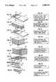
- FIG. 1, including FIGS. 1(a)-1(h),comprises a sequence of perspective schematic views illustrating the principal stages in fabrication of a multiple-element transducer according to the invention
- FIG. 2including FIGS. 2(a)-2(h), comprises a corresponding sequence of verbal descriptions of the principal stages in fabrication of a multiple-element transducer according to the invention
- FIG. 3is a cross-sectional view of the distal tip of an ultrasonic probe comprising a multiple-element piezoelectric transducer according to the invention.
- FIG. 4is a view corresponding to FIG. 3, illustrating a somewhat different embodiment of the invention.
- FIGS. 1 and 2provide corresponding schematic illustrations and verbal explanations of the stages in fabrication of multiple-element piezoelectric transducers according to the invention.
- FIGS. 1(a) and 2(a)describe the formation of a green precursor tape.
- the desired piezoelectric ceramic material to be preparedis lead zirconate-titanate (PZT).
- PZTlead zirconate-titanate
- a PZT powderis prepared by mixing and calcining PbO, TiO 2 , ZrO 2 , and small quantities of modifier oxides in the appropriate proportions.
- the properties of the PZTcan be varied by suitably varying the ratios of the constituent oxides.
- the calcined PZTis then processed to form a PZT powder, e.g., by ball milling.
- the PZT powderis further mixed with known organic solvents, plasticizers, binders and the like to form a slurry.
- the slurryis then poured onto a substrate 14 moving with respect to a pair of double doctor blades 12 in a generally conventional tape casting system 10, the slurry thus forming the "slip" of the tape-casting process.
- the slipis confined between a dam 18 and the doctor blades 12, so that as the substrate 14 passes slowly beneath the doctor blades 12, a green precursor tape 16 is formed, the tape 16 being of very consistent thickness.
- the green precursor tape 16is then dried; typically air-drying is sufficient.
- the dried green precursor tape 16is then cut into strips 20, which are stacked, interposed with spacers 22 of previously sintered PZT material, after which the stack is sintered, such that the green precursor strips 20 are converted to sintered ceramic PZT plates.
- spacers 22of previously sintered PZT material, after which the stack is sintered, such that the green precursor strips 20 are converted to sintered ceramic PZT plates.
- the green precursor stripsare prepared as a thin (e.g., 100 micron) tape 16, which is subsequently cut into strips and fired. Since such a thin tape has a relatively high ratio of surface area to volume, the problem of Pb loss during sintering will be particularly acute if not avoided. Further, the thin PZT plates resulting from sintering of such a thin tape are not strong enough to be lapped, whereby a Pb-depleted surface layer might be removed. According to the invention, Pb-containing previously sintered PZT spacers 22 are provided in direct contact with the green precursor strips 20 during the sintering step.
- the PZT spacers 22separate the green precursor strips 20, minimize Pb loss, and constrain the PZT plates formed upon sintering of the strips 20 to remain flat, such that lapping of the PZT plates is unnecessary.
- the green precursor strips 20shrink substantially during sintering, such that the PZT plates formed do not tend to adhere to the previously sintered PZT spacers 22.
- the sintering stepmay be carried out by placing the stacked green precursor strips 20 and previously sintered PZT spacers 22 in an alumina crucible, placing the crucible in a sintering furnace having an oxidizing atmosphere, and gradually raising the temperature to on the order of 500° C. to volatilize and remove the organic binders, plasticizers, and the like used to provide a workable slurry. The temperature may then be raised to substantially 1250° C. and maintained for on the order of 0.5 hour, to densify and solidify the green precursor material, forming solid PZT plates between the previously sintered PZT spacers 22.
- PZT platesmay be produced having piezoelectric properties which are not compromised by the mechanical steps necessary for their production.
- the same processmay be employed for preparing plates of other ceramic materials, such as modified lead titanates, e.g., (Pb,Ca)TiO 3 and (Pb,Sm)TiO 3 , lead metaniobate, or barium titanate, which are used for other purposes.
- modified lead titanatese.g., (Pb,Ca)TiO 3 and (Pb,Sm)TiO 3
- lead metaniobatee.g., lead metaniobate, or barium titanate
- FIGS. 1(d)-(h) and 2(d)-(h)illustrate the principal steps performed in fabrication of multiple-element piezoelectric transducers using PZT plates produced using the methods described above.
- the sintered PZT plates 30are assembled in a stack 34, the PZT plates 30 being interposed with layers 32 of a thermoplastic polymer, such as polyvinyl butyral (PVB) or polyvinyl formal (PVF).
- PVBpolyvinyl butyral
- PVFpolyvinyl formal
- the PVB or PVF materialmay be prepared as a sheet 28, using a tape-casting process as discussed generally above, but this is not a limitation on the invention. Tape-casting the polymer allows selection from a wide range of polymer thicknesses, and allows convenient introduction of plasticizers and fillers to tailor the acoustic impedance and attenuative properties of the polymer sheets.
- the stack 34 of alternating PZT plates 30 and polymer layers 32is then placed in a furnace and baked to reach a temperature at least equal to the melting point of the polymer material (for example, 160° C. for PVB or 210° C. for PVF), such that the polymer when cooled bonds the PZT plates 30 into a solid block 36.
- axial compressionmay be applied during the baking step, and this step may be carried out under vacuum, to improve the properties of the block 36.
- the polymerboth provides a passive material separating the PZT plates and bonds the PZT plates into a unitary block.
- the block 36 having plates 30 of PZT interspersed with passive polymer layers 32is referred to in the art as a "2--2 composite". If prepared as indicated, no voids will exist between the plates 30 of the PZT ceramic material.
- the block 36is then slit into elongated laminate members 40 comprising alternating PZT elements 42 and polymer layers 44, in two slitting steps.
- the block 36is first slit along a number of parallel first cutting planes perpendicular to the planes of the plates of PZT material and polymer (FIG. 1(e) ), forming slabs 38 comprising alternate layers of the PZT and polymer materials.
- the slabs 38are then slit along a number of parallel second cutting planes perpendicular to the first cutting planes and to the planes of the plates of PZT material and polymer (FIG. 1(f)), forming elongated laminate members 40, of generally square cross-section, having alternate PZT elements 42 spaced by layers 44 of polymer extending along their length.
- front and rear electrodesare then applied to each elongated laminate member 40 to fabricate a multiple-element transducer.
- the front electrode 46may comprise a continuous metallized surface applied by electroless plating, sputtering, or vapor deposition directly to one side of the elongated laminated member 40.
- Individual rear electrodes 48are connected to the PZT elements 42.
- the transduceris completed by impedance matching layers 62 and 64 and a backing layer 60, as illustrated in FIGS. 1(h) and 2(h).
- the rear electrodes 48may comprise individual traces printed on a flex circuit element 50 (i.e., individual conductors formed as part of a printed circuit on a flexible substrate) at the same spacing as the PZT elements 42 and bonded thereto by a film 56 of a commercially available anisotropically conductive adhesive material, e.g., "Z-Axis Adhesive Film” available as Part No. 5303R from the 3M Corporation. See FIG. 3.
- This method of connecting the electrodes 48 to the PZT elements 42requires that the pitch (i.e., the spacing) of the electrodes 48 and PZT elements 42 be equal over the length of the transducer assembly.
- the PZT elements 42may be formed at substantially finer pitch than the rear electrodes 58, such that each electrode 58 is connected (using the same conductive adhesive) to several, typically two or three, of the PZT elements 42. Connecting each electrode 58 to several of the PZT elements 42 renders the relative pitch thereof less critical.
- FIG. 4also illustrates an alternative method of forming the electrodes 58, namely by printing directly onto a ceramic substrate 54. The electrodes 58 and the conductors 70 to which the electrodes are connected might also be printed directly onto a backing layer 60 typically applied to protect the rear surface of the laminate member 40. Backing layer 60 is typically also provided in the embodiment of FIG. 3, as shown.
- a multiple-element transducer 66is completed by one or more layers 62, 64 of acoustic impedance matching materials. Layers 62, 64 are provided in order to match the very high acoustic impedance of the hard ceramic elements 42 to the material with which the transducer 66 is intended to be used. Where the transducer 66 is to be used for medical imaging purposes, such that the transducer 66 will function to transmit ultrasonic energy into body tissues and detect reflection of energy from internal structures and the like, suitable impedance matching layers 62 and 64 may be formed of glass and epoxy, respectively, as generally known in the art. As noted above, a backing layer 60 is commonly provided as well; a suitable material is tungsten-loaded epoxy, again as generally known in the art.
- a complete transducer 66may include a single elongate laminate assembly as described above, for emitting energy into a structure to be examined and detecting energy reflected therefrom, may comprise several such assemblies arranged in line with one another, providing a longer one-dimensional array of transducer elements, or may comprise a number of such assemblies in a two-dimensional array.
- the transducer 66may be conveniently mounted at the distal tip of a probe 68, for being maneuvered into contact with tissues or other structures to be imaged or otherwise examined using energy emitted by the transducer 66.
- Conductors 70 connected to the electrodes 46, 48pass through a lumen extending along the axis of probe 68 and are connected to excitation and analysis circuitry, for supplying energy transmitted into the structure to be examined and analysis of the reflected energy, all generally as known in the art.
- pulses of high-frequency energywill be applied between the front electrode 46 and selected ones of the rear electrodes 48, to cause the corresponding PZT elements 42 to transmit bursts of ultrasonic energy into the structure to be examined; electrical signals emitted by each of the PZT elements 42 responsive to detection of reflected energy are then transmitted by conductors 70 to data analysis and imaging equipment, again generally as known to the art.
Landscapes
- Health & Medical Sciences (AREA)
- Engineering & Computer Science (AREA)
- Life Sciences & Earth Sciences (AREA)
- Molecular Biology (AREA)
- Animal Behavior & Ethology (AREA)
- Nuclear Medicine, Radiotherapy & Molecular Imaging (AREA)
- Pathology (AREA)
- Radiology & Medical Imaging (AREA)
- Physics & Mathematics (AREA)
- Biomedical Technology (AREA)
- Heart & Thoracic Surgery (AREA)
- Medical Informatics (AREA)
- Gynecology & Obstetrics (AREA)
- Surgery (AREA)
- Biophysics (AREA)
- General Health & Medical Sciences (AREA)
- Public Health (AREA)
- Veterinary Medicine (AREA)
- Mechanical Engineering (AREA)
- Chemical & Material Sciences (AREA)
- Composite Materials (AREA)
- Materials Engineering (AREA)
- Manufacturing & Machinery (AREA)
- Ultra Sonic Daignosis Equipment (AREA)
- Transducers For Ultrasonic Waves (AREA)
Abstract
Description
Claims (28)
Priority Applications (1)
| Application Number | Priority Date | Filing Date | Title |
|---|---|---|---|
| US08/046,965US5359760A (en) | 1993-04-16 | 1993-04-16 | Method of manufacture of multiple-element piezoelectric transducer |
Applications Claiming Priority (1)
| Application Number | Priority Date | Filing Date | Title |
|---|---|---|---|
| US08/046,965US5359760A (en) | 1993-04-16 | 1993-04-16 | Method of manufacture of multiple-element piezoelectric transducer |
Publications (1)
| Publication Number | Publication Date |
|---|---|
| US5359760Atrue US5359760A (en) | 1994-11-01 |
Family
ID=21946325
Family Applications (1)
| Application Number | Title | Priority Date | Filing Date |
|---|---|---|---|
| US08/046,965Expired - Fee RelatedUS5359760A (en) | 1993-04-16 | 1993-04-16 | Method of manufacture of multiple-element piezoelectric transducer |
Country Status (1)
| Country | Link |
|---|---|
| US (1) | US5359760A (en) |
Cited By (45)
| Publication number | Priority date | Publication date | Assignee | Title |
|---|---|---|---|---|
| US5617865A (en)* | 1995-03-31 | 1997-04-08 | Siemens Medical Systems, Inc. | Multi-dimensional ultrasonic array interconnect |
| US5625149A (en)* | 1994-07-27 | 1997-04-29 | Hewlett-Packard Company | Ultrasonic transductor |
| US5638822A (en)* | 1995-06-30 | 1997-06-17 | Hewlett-Packard Company | Hybrid piezoelectric for ultrasonic probes |
| US5758396A (en)* | 1993-05-04 | 1998-06-02 | Daewoo Electronics Co., Ltd. | Method of manufacturing a piezoelectric actuator array |
| US5771567A (en)* | 1996-08-29 | 1998-06-30 | Raytheon Company | Methods of fabricating continuous transverse stub radiating structures and antennas |
| US5779644A (en)* | 1993-02-01 | 1998-07-14 | Endosonics Coporation | Ultrasound catheter probe |
| US5825121A (en)* | 1994-07-08 | 1998-10-20 | Seiko Epson Corporation | Thin film piezoelectric device and ink jet recording head comprising the same |
| US5844349A (en)* | 1997-02-11 | 1998-12-01 | Tetrad Corporation | Composite autoclavable ultrasonic transducers and methods of making |
| US5857974A (en)* | 1997-01-08 | 1999-01-12 | Endosonics Corporation | High resolution intravascular ultrasound transducer assembly having a flexible substrate |
| US6161270A (en)* | 1999-01-29 | 2000-12-19 | Eastman Kodak Company | Making printheads using tapecasting |
| US6176986B1 (en)* | 1996-05-27 | 2001-01-23 | Mitsubishi Materials Corporation | Sputtering target of dielectrics having high strength and a method for manufacturing same |
| US20020010990A1 (en)* | 1998-12-28 | 2002-01-31 | Ngk Insulators, Ltd. | Piezoelectric/electrostrictive device and production method thereof |
| US6370748B1 (en)* | 1999-04-02 | 2002-04-16 | Gisulfo Baccini | Device to produce multi-layer electronic circuits |
| US6390985B1 (en)* | 1999-07-21 | 2002-05-21 | Scimed Life Systems, Inc. | Impedance matching transducers |
| US6406433B1 (en)* | 1999-07-21 | 2002-06-18 | Scimed Life Systems, Inc. | Off-aperture electrical connect transducer and methods of making |
| US6447712B1 (en) | 1998-12-28 | 2002-09-10 | University Of Washington | Method for sintering ceramic tapes |
| US6494566B1 (en)* | 1997-01-31 | 2002-12-17 | Kyocera Corporation | Head member having ultrafine grooves and a method of manufacture thereof |
| US6498547B2 (en)* | 2000-01-18 | 2002-12-24 | Murata Manufacturing Co., Ltd. | Anisotropically electroconductive adhesive and a ladder filter using the same |
| US6538363B2 (en)* | 2000-09-28 | 2003-03-25 | Matsushita Electric Industrial Co., Ltd. | Method of manufacturing a piezoelectric element |
| US20040040132A1 (en)* | 1999-10-29 | 2004-03-04 | Usa As Represented By The Administrator Of The National Aeronautics And Space Administration | Piezoelectric composite apparatus and a method for fabricating the same |
| US6733456B1 (en) | 1998-07-31 | 2004-05-11 | Scimed Life Systems, Inc. | Off-aperture electrical connection for ultrasonic transducer |
| US6776763B2 (en)* | 1994-03-11 | 2004-08-17 | Volcano Therapeutic, Inc. | Ultrasonic transducer array and method of manufacturing the same |
| US20040254471A1 (en)* | 2003-06-13 | 2004-12-16 | Andreas Hadjicostis | Miniature ultrasonic phased array for intracardiac and intracavity applications |
| US20050099097A1 (en)* | 2003-11-11 | 2005-05-12 | Baumgartner Charles E. | Method for making multi-layer ceramic acoustic transducer |
| US20050115039A1 (en)* | 2003-11-28 | 2005-06-02 | Kazuhiro Okuda | Method of producing piezoelectric ceramic device |
| US7002696B1 (en)* | 2000-11-03 | 2006-02-21 | Optune Technologies | Band pass interferometer with tuning capabilities |
| US7003857B1 (en)* | 1995-11-24 | 2006-02-28 | Seiko Epson Corporation | Method of producing an ink-jet printing head |
| US20060100522A1 (en)* | 2004-11-08 | 2006-05-11 | Scimed Life Systems, Inc. | Piezocomposite transducers |
| US20060261707A1 (en)* | 2004-08-27 | 2006-11-23 | Wildes Douglas G | Ultrasound transducer with enhanced thermal conductivity |
| US7226417B1 (en) | 1995-12-26 | 2007-06-05 | Volcano Corporation | High resolution intravascular ultrasound transducer assembly having a flexible substrate |
| US7229437B2 (en) | 2003-09-22 | 2007-06-12 | St. Jude Medical, Atrial Fibrillation Division, Inc. | Medical device having integral traces and formed electrodes |
| US7234225B2 (en)* | 2003-09-22 | 2007-06-26 | St. Jude Medical, Atrial Fibrillation Division, Inc. | Method for manufacturing medical device having embedded traces and formed electrodes |
| US20080123104A1 (en)* | 2006-11-27 | 2008-05-29 | Roctest Ltee | High selectivity band-pass interferometer with tuning capabilities |
| US20090030312A1 (en)* | 2007-07-27 | 2009-01-29 | Andreas Hadjicostis | Image-guided intravascular therapy catheters |
| US20090113710A1 (en)* | 2007-11-06 | 2009-05-07 | Xerox Corporation | Method for fabricating a transducer with improved thickness uniformity |
| US20090131319A1 (en)* | 1995-06-05 | 2009-05-21 | Human Genome Sciences, Inc. | Human Tumor Necrosis Factor Receptor-Like 2 |
| US20090183350A1 (en)* | 2008-01-17 | 2009-07-23 | Wetsco, Inc. | Method for Ultrasound Probe Repair |
| US20110206888A1 (en)* | 2010-02-22 | 2011-08-25 | Marshall Suarez | Composite Ceramic Structure and Method of Making the Same |
| US8147486B2 (en) | 2003-09-22 | 2012-04-03 | St. Jude Medical, Atrial Fibrillation Division, Inc. | Medical device with flexible printed circuit |
| CN103682082A (en)* | 2013-12-02 | 2014-03-26 | 南京航空航天大学 | Method for producing macro piezoelectric ceramic fiber composite actuator |
| US8813324B2 (en) | 2010-03-24 | 2014-08-26 | Western Digital (Fremont), Llc | Method for providing a piezoelectric multilayer |
| US10188368B2 (en) | 2017-06-26 | 2019-01-29 | Andreas Hadjicostis | Image guided intravascular therapy catheter utilizing a thin chip multiplexor |
| EP3519110A1 (en)* | 2016-09-29 | 2019-08-07 | Koninklijke Philips N.V. | Flexible phased array transducer for intravascular imaging device and associated devices, systems, and methods |
| US10492760B2 (en) | 2017-06-26 | 2019-12-03 | Andreas Hadjicostis | Image guided intravascular therapy catheter utilizing a thin chip multiplexor |
| US11109909B1 (en) | 2017-06-26 | 2021-09-07 | Andreas Hadjicostis | Image guided intravascular therapy catheter utilizing a thin ablation electrode |
Citations (10)
| Publication number | Priority date | Publication date | Assignee | Title |
|---|---|---|---|---|
| US4353958A (en)* | 1979-02-22 | 1982-10-12 | Narumi China Corporation | Green ceramic tapes and method of producing them |
| US4359271A (en)* | 1979-10-18 | 1982-11-16 | Olympus Optical Co., Ltd. | Compact photographic camera lens system having a short overall length |
| US4514247A (en)* | 1983-08-15 | 1985-04-30 | North American Philips Corporation | Method for fabricating composite transducers |
| US4518889A (en)* | 1982-09-22 | 1985-05-21 | North American Philips Corporation | Piezoelectric apodized ultrasound transducers |
| US4564980A (en)* | 1980-06-06 | 1986-01-21 | Siemens Aktiengesellschaft | Ultrasonic transducer system and manufacturing method |
| US4717851A (en)* | 1986-04-30 | 1988-01-05 | Siemens Aktiengesellschaft | Adaptation layer for an ultrasound applicator |
| US4747192A (en)* | 1983-12-28 | 1988-05-31 | Kabushiki Kaisha Toshiba | Method of manufacturing an ultrasonic transducer |
| US4939826A (en)* | 1988-03-04 | 1990-07-10 | Hewlett-Packard Company | Ultrasonic transducer arrays and methods for the fabrication thereof |
| US4977655A (en)* | 1986-04-25 | 1990-12-18 | Intra-Sonix, Inc. | Method of making a transducer |
| US5153859A (en)* | 1989-03-29 | 1992-10-06 | Atochem North America, Inc. | Laminated piezoelectric structure and process of forming the same |
- 1993
- 1993-04-16USUS08/046,965patent/US5359760A/ennot_activeExpired - Fee Related
Patent Citations (11)
| Publication number | Priority date | Publication date | Assignee | Title |
|---|---|---|---|---|
| US4353958A (en)* | 1979-02-22 | 1982-10-12 | Narumi China Corporation | Green ceramic tapes and method of producing them |
| US4359271A (en)* | 1979-10-18 | 1982-11-16 | Olympus Optical Co., Ltd. | Compact photographic camera lens system having a short overall length |
| US4564980A (en)* | 1980-06-06 | 1986-01-21 | Siemens Aktiengesellschaft | Ultrasonic transducer system and manufacturing method |
| US4518889A (en)* | 1982-09-22 | 1985-05-21 | North American Philips Corporation | Piezoelectric apodized ultrasound transducers |
| US4514247A (en)* | 1983-08-15 | 1985-04-30 | North American Philips Corporation | Method for fabricating composite transducers |
| US4572981A (en)* | 1983-08-15 | 1986-02-25 | North American Philips Corporation | Transducer comprising composite electrical materials |
| US4747192A (en)* | 1983-12-28 | 1988-05-31 | Kabushiki Kaisha Toshiba | Method of manufacturing an ultrasonic transducer |
| US4977655A (en)* | 1986-04-25 | 1990-12-18 | Intra-Sonix, Inc. | Method of making a transducer |
| US4717851A (en)* | 1986-04-30 | 1988-01-05 | Siemens Aktiengesellschaft | Adaptation layer for an ultrasound applicator |
| US4939826A (en)* | 1988-03-04 | 1990-07-10 | Hewlett-Packard Company | Ultrasonic transducer arrays and methods for the fabrication thereof |
| US5153859A (en)* | 1989-03-29 | 1992-10-06 | Atochem North America, Inc. | Laminated piezoelectric structure and process of forming the same |
Non-Patent Citations (5)
| Title |
|---|
| A Precision Tape Casting Machine for Fabricating Thin Ceramic Tapes, R. B. Runk and M. J. Andrejco, Western Electric Co., Engineering Research Center, Princeton, N.J., Ceramic Bulletin, vol. 54, No. 2 (1975).* |
| Processing Parameters and Electric Properties of Doctor Bladed Ferroelectric Ceramics, Chandler Wentworth and George W. Taylor, RCA Laboratories, Princeton, N.J., Ceramic Bulletin, vol. 46, No. 12 (1967).* |
| Processing Parameters and Electric Properties of Doctor-Bladed Ferroelectric Ceramics, Chandler Wentworth and George W. Taylor, RCA Laboratories, Princeton, N.J., Ceramic Bulletin, vol. 46, No. 12 (1967). |
| Tape Casting, Richard E. Mistler, Keramos Industries, Inc., reprinted from Engineered Materials Handbook, The Materials Information Society, vol. 4: Ceramics and Glasses.* |
| Tape Casting: The Basic Process for Meeting the Needs of the Electronics Industry, Richard E. Mistler, Keramos Industries, Inc., Morrisville, Pa. 19067, Ceramic Bulletin, vol. 69, No. 6, 1990.* |
Cited By (64)
| Publication number | Priority date | Publication date | Assignee | Title |
|---|---|---|---|---|
| US5779644A (en)* | 1993-02-01 | 1998-07-14 | Endosonics Coporation | Ultrasound catheter probe |
| US5758396A (en)* | 1993-05-04 | 1998-06-02 | Daewoo Electronics Co., Ltd. | Method of manufacturing a piezoelectric actuator array |
| US6776763B2 (en)* | 1994-03-11 | 2004-08-17 | Volcano Therapeutic, Inc. | Ultrasonic transducer array and method of manufacturing the same |
| US6149968A (en)* | 1994-07-08 | 2000-11-21 | Seiko Epson Corporation | Thin film piezoelectric device and ink jet recording head comprising the same |
| US5825121A (en)* | 1994-07-08 | 1998-10-20 | Seiko Epson Corporation | Thin film piezoelectric device and ink jet recording head comprising the same |
| US5625149A (en)* | 1994-07-27 | 1997-04-29 | Hewlett-Packard Company | Ultrasonic transductor |
| US5617865A (en)* | 1995-03-31 | 1997-04-08 | Siemens Medical Systems, Inc. | Multi-dimensional ultrasonic array interconnect |
| US20090131319A1 (en)* | 1995-06-05 | 2009-05-21 | Human Genome Sciences, Inc. | Human Tumor Necrosis Factor Receptor-Like 2 |
| US5638822A (en)* | 1995-06-30 | 1997-06-17 | Hewlett-Packard Company | Hybrid piezoelectric for ultrasonic probes |
| US7003857B1 (en)* | 1995-11-24 | 2006-02-28 | Seiko Epson Corporation | Method of producing an ink-jet printing head |
| US7226417B1 (en) | 1995-12-26 | 2007-06-05 | Volcano Corporation | High resolution intravascular ultrasound transducer assembly having a flexible substrate |
| US20110034809A1 (en)* | 1995-12-26 | 2011-02-10 | Volcano Corporation | High Resolution Intravascular Ultrasound Transducer Assembly Having A Flexible Substrate |
| US7846101B2 (en) | 1995-12-26 | 2010-12-07 | Volcano Corporation | High resolution intravascular ultrasound transducer assembly having a flexible substrate |
| US6176986B1 (en)* | 1996-05-27 | 2001-01-23 | Mitsubishi Materials Corporation | Sputtering target of dielectrics having high strength and a method for manufacturing same |
| US5771567A (en)* | 1996-08-29 | 1998-06-30 | Raytheon Company | Methods of fabricating continuous transverse stub radiating structures and antennas |
| US20050197574A1 (en)* | 1997-01-08 | 2005-09-08 | Volcano Corporation | Ultrasound transducer array having a flexible substrate |
| US6049958A (en)* | 1997-01-08 | 2000-04-18 | Endosonics Corporation | High resolution intravascular ultrasound transducer assembly having a flexible substrate and method for manufacture thereof |
| US5857974A (en)* | 1997-01-08 | 1999-01-12 | Endosonics Corporation | High resolution intravascular ultrasound transducer assembly having a flexible substrate |
| US6899682B2 (en) | 1997-01-08 | 2005-05-31 | Volcano Therapeutics, Inc. | Intravascular ultrasound transducer assembly having a flexible substrate and method for manufacturing such assembly |
| US6618916B1 (en) | 1997-01-08 | 2003-09-16 | Jomed Inc. | Method for manufacturing a high resolution intravascular ultrasound transducer assembly having a flexible substrate |
| US6494566B1 (en)* | 1997-01-31 | 2002-12-17 | Kyocera Corporation | Head member having ultrafine grooves and a method of manufacture thereof |
| US5844349A (en)* | 1997-02-11 | 1998-12-01 | Tetrad Corporation | Composite autoclavable ultrasonic transducers and methods of making |
| US6088894A (en)* | 1997-02-11 | 2000-07-18 | Tetrad Corporation | Methods of making composite ultrasonic transducers |
| US6733456B1 (en) | 1998-07-31 | 2004-05-11 | Scimed Life Systems, Inc. | Off-aperture electrical connection for ultrasonic transducer |
| US6447712B1 (en) | 1998-12-28 | 2002-09-10 | University Of Washington | Method for sintering ceramic tapes |
| US20020010990A1 (en)* | 1998-12-28 | 2002-01-31 | Ngk Insulators, Ltd. | Piezoelectric/electrostrictive device and production method thereof |
| US6925693B2 (en)* | 1998-12-28 | 2005-08-09 | Ngk Insulators, Ltd. | Method of fabricating a piezoelectric/electrostrictive device |
| US6161270A (en)* | 1999-01-29 | 2000-12-19 | Eastman Kodak Company | Making printheads using tapecasting |
| US6370748B1 (en)* | 1999-04-02 | 2002-04-16 | Gisulfo Baccini | Device to produce multi-layer electronic circuits |
| US6390985B1 (en)* | 1999-07-21 | 2002-05-21 | Scimed Life Systems, Inc. | Impedance matching transducers |
| US6406433B1 (en)* | 1999-07-21 | 2002-06-18 | Scimed Life Systems, Inc. | Off-aperture electrical connect transducer and methods of making |
| US7197798B2 (en)* | 1999-10-29 | 2007-04-03 | United States Of America As Represented By The Administrator Of The National Aeronautics And Space Administration | Method of fabricating a composite apparatus |
| US20040040132A1 (en)* | 1999-10-29 | 2004-03-04 | Usa As Represented By The Administrator Of The National Aeronautics And Space Administration | Piezoelectric composite apparatus and a method for fabricating the same |
| US6498547B2 (en)* | 2000-01-18 | 2002-12-24 | Murata Manufacturing Co., Ltd. | Anisotropically electroconductive adhesive and a ladder filter using the same |
| US6538363B2 (en)* | 2000-09-28 | 2003-03-25 | Matsushita Electric Industrial Co., Ltd. | Method of manufacturing a piezoelectric element |
| US7002696B1 (en)* | 2000-11-03 | 2006-02-21 | Optune Technologies | Band pass interferometer with tuning capabilities |
| US20040254471A1 (en)* | 2003-06-13 | 2004-12-16 | Andreas Hadjicostis | Miniature ultrasonic phased array for intracardiac and intracavity applications |
| US8221408B2 (en) | 2003-09-22 | 2012-07-17 | St. Jude Medical, Atrial Fibrillation Division, Inc. | Medical device having integral traces and formed electrodes |
| US8147486B2 (en) | 2003-09-22 | 2012-04-03 | St. Jude Medical, Atrial Fibrillation Division, Inc. | Medical device with flexible printed circuit |
| US7229437B2 (en) | 2003-09-22 | 2007-06-12 | St. Jude Medical, Atrial Fibrillation Division, Inc. | Medical device having integral traces and formed electrodes |
| US7234225B2 (en)* | 2003-09-22 | 2007-06-26 | St. Jude Medical, Atrial Fibrillation Division, Inc. | Method for manufacturing medical device having embedded traces and formed electrodes |
| US7669309B2 (en) | 2003-09-22 | 2010-03-02 | St. Jude Medical, Atrial Fibrillation Division, Inc. | Method for manufacturing a medical device having integral traces and formed electrodes |
| US7156938B2 (en)* | 2003-11-11 | 2007-01-02 | General Electric Company | Method for making multi-layer ceramic acoustic transducer |
| US20050099097A1 (en)* | 2003-11-11 | 2005-05-12 | Baumgartner Charles E. | Method for making multi-layer ceramic acoustic transducer |
| US7305743B2 (en)* | 2003-11-28 | 2007-12-11 | Matsushita Electric Industrial Co., Ltd. | Method of producing piezoelectric ceramic device |
| US20050115039A1 (en)* | 2003-11-28 | 2005-06-02 | Kazuhiro Okuda | Method of producing piezoelectric ceramic device |
| US20060261707A1 (en)* | 2004-08-27 | 2006-11-23 | Wildes Douglas G | Ultrasound transducer with enhanced thermal conductivity |
| US7694406B2 (en)* | 2004-08-27 | 2010-04-13 | General Electric Company | Method for forming a composite structure of backing material for use in a transducer assembly |
| US20060100522A1 (en)* | 2004-11-08 | 2006-05-11 | Scimed Life Systems, Inc. | Piezocomposite transducers |
| US20080123104A1 (en)* | 2006-11-27 | 2008-05-29 | Roctest Ltee | High selectivity band-pass interferometer with tuning capabilities |
| US20090030312A1 (en)* | 2007-07-27 | 2009-01-29 | Andreas Hadjicostis | Image-guided intravascular therapy catheters |
| US8702609B2 (en) | 2007-07-27 | 2014-04-22 | Meridian Cardiovascular Systems, Inc. | Image-guided intravascular therapy catheters |
| US20090113710A1 (en)* | 2007-11-06 | 2009-05-07 | Xerox Corporation | Method for fabricating a transducer with improved thickness uniformity |
| US7992287B2 (en)* | 2007-11-06 | 2011-08-09 | Xerox Corporation | System for thinning a transducer with improved thickness uniformity |
| US20090183350A1 (en)* | 2008-01-17 | 2009-07-23 | Wetsco, Inc. | Method for Ultrasound Probe Repair |
| US20110206888A1 (en)* | 2010-02-22 | 2011-08-25 | Marshall Suarez | Composite Ceramic Structure and Method of Making the Same |
| US8561270B2 (en)* | 2010-02-22 | 2013-10-22 | Cts Corporation | Composite ceramic structure and method of making the same |
| US8813324B2 (en) | 2010-03-24 | 2014-08-26 | Western Digital (Fremont), Llc | Method for providing a piezoelectric multilayer |
| CN103682082A (en)* | 2013-12-02 | 2014-03-26 | 南京航空航天大学 | Method for producing macro piezoelectric ceramic fiber composite actuator |
| EP3519110A1 (en)* | 2016-09-29 | 2019-08-07 | Koninklijke Philips N.V. | Flexible phased array transducer for intravascular imaging device and associated devices, systems, and methods |
| US11497470B2 (en) | 2016-09-29 | 2022-11-15 | Koninklijke Philips N.V. | Flexible phased array transducer for intravascular imaging device and associated devices, systems, and methods |
| US10188368B2 (en) | 2017-06-26 | 2019-01-29 | Andreas Hadjicostis | Image guided intravascular therapy catheter utilizing a thin chip multiplexor |
| US10492760B2 (en) | 2017-06-26 | 2019-12-03 | Andreas Hadjicostis | Image guided intravascular therapy catheter utilizing a thin chip multiplexor |
| US11109909B1 (en) | 2017-06-26 | 2021-09-07 | Andreas Hadjicostis | Image guided intravascular therapy catheter utilizing a thin ablation electrode |
Similar Documents
| Publication | Publication Date | Title |
|---|---|---|
| US5359760A (en) | Method of manufacture of multiple-element piezoelectric transducer | |
| US6225728B1 (en) | Composite piezoelectric transducer arrays with improved acoustical and electrical impedance | |
| US5539965A (en) | Method for making piezoelectric composites | |
| EP1642531B1 (en) | Ultrasonic probe and ultrasonic diagnostic aparatus | |
| US6868594B2 (en) | Method for making a transducer | |
| EP1066119B1 (en) | Arrays made from flexible transducer elements | |
| US9972766B2 (en) | Piezoelectric transducer, ultrasonic probe, and piezoelectric transducer manufacturing method | |
| EP1227525B1 (en) | Piezocomposite, ultrasonic probe for ultrasonic diagnostic equipment, ultrasonic diagnostic equipment and method for producing piezocomposite | |
| US7581295B2 (en) | Piezoelectric element and method of manufacturing the same | |
| JP5347503B2 (en) | Ultrasonic probe and method of manufacturing ultrasonic probe | |
| CN103041978A (en) | Focusing ultrasonic transducer and producing method thereof | |
| Safari et al. | Development of fine‐scale piezoelectric composites for transducers | |
| JP4771649B2 (en) | Manufacturing method of multilayer electronic component | |
| JP3420866B2 (en) | Ultrasonic probe | |
| CN1050008C (en) | Piezoelectric/electrostrictive film element and method of producing the same | |
| WO2003042687A1 (en) | Ultrasonic probe | |
| Stevenson et al. | Fabrication and characterization of PZT/Thermoplastic polymer composites for high‐frequency phased linear arrays | |
| JP3419327B2 (en) | Porcelain material, ultrasonic probe, piezoelectric vibrator, and methods of manufacturing them | |
| Hackenberger et al. | 2-2 PZT-polymer composites for high frequency (> 20 MHz) ultrasound transducers | |
| CN1129359A (en) | Piezoelectric/electrostrictive film element having convex diaphragm portions and method of producing the same | |
| JP3943731B2 (en) | Piezoelectric plate for ultrasonic transducer and manufacturing method thereof | |
| JP2004104629A (en) | Ultrasonic probe | |
| JP3679957B2 (en) | Ultrasonic probe and manufacturing method thereof | |
| Huebner et al. | Fabrication of 2-2 connectivity PZT/thermoplastic composites for high frequency linear arrays | |
| JP2013026682A (en) | Medical composite single-crystal piezoelectric vibrator, medical ultrasonic probe, method of manufacturing medical composite single-crystal piezoelectric vibrator, and method of manufacturing medical ultrasonic probe |
Legal Events
| Date | Code | Title | Description |
|---|---|---|---|
| AS | Assignment | Owner name:CURATORS OF THE UNVIVERSITY OF MISSOURI ON BEHALF Free format text:ASSIGNMENT OF ASSIGNORS INTEREST;ASSIGNORS:BUSSE, LAWRENCE J.;STEVENSON, JEFFRY W.;HUEBNER, WAYNE;REEL/FRAME:006686/0019 Effective date:19930708 | |
| AS | Assignment | Owner name:SILICON VALLEY BANK, CALIFORNIA Free format text:SECURITY INTEREST;ASSIGNOR:TETRAD CORPORATION, A DELAWARE CORPORATION;REEL/FRAME:007312/0417 Effective date:19940909 | |
| REMI | Maintenance fee reminder mailed | ||
| LAPS | Lapse for failure to pay maintenance fees | ||
| FP | Lapsed due to failure to pay maintenance fee | Effective date:19981101 | |
| AS | Assignment | Owner name:NATIONAL INSTITUTES OF HEALTH (NIH), U.S. DEPT. OF Free format text:EXECUTIVE ORDER 9424, CONFIRMATORY LICENSE;ASSIGNOR:TETRAD CORPORATION;REEL/FRAME:020960/0412 Effective date:19940610 | |
| AS | Assignment | Owner name:NATIONAL INSTITUTES OF HEALTH (NIH), U.S. DEPT. OF Free format text:CONFIRMATORY LICENSE;ASSIGNOR:TETRAD CORPORATION;REEL/FRAME:026358/0085 Effective date:19940610 | |
| STCH | Information on status: patent discontinuation | Free format text:PATENT EXPIRED DUE TO NONPAYMENT OF MAINTENANCE FEES UNDER 37 CFR 1.362 |