US5359631A - Timing recovery circuit for synchronous waveform sampling - Google Patents
Timing recovery circuit for synchronous waveform samplingDownload PDFInfo
- Publication number
- US5359631A US5359631AUS07/954,350US95435092AUS5359631AUS 5359631 AUS5359631 AUS 5359631AUS 95435092 AUS95435092 AUS 95435092AUS 5359631 AUS5359631 AUS 5359631A
- Authority
- US
- United States
- Prior art keywords
- signal
- samples
- pulse
- frequency
- error measurement
- Prior art date
- Legal status (The legal status is an assumption and is not a legal conclusion. Google has not performed a legal analysis and makes no representation as to the accuracy of the status listed.)
- Expired - Lifetime
Links
Images


Classifications
- G—PHYSICS
- G11—INFORMATION STORAGE
- G11B—INFORMATION STORAGE BASED ON RELATIVE MOVEMENT BETWEEN RECORD CARRIER AND TRANSDUCER
- G11B20/00—Signal processing not specific to the method of recording or reproducing; Circuits therefor
- G11B20/10—Digital recording or reproducing
- G11B20/10009—Improvement or modification of read or write signals
- G11B20/10037—A/D conversion, D/A conversion, sampling, slicing and digital quantisation or adjusting parameters thereof
- G—PHYSICS
- G11—INFORMATION STORAGE
- G11B—INFORMATION STORAGE BASED ON RELATIVE MOVEMENT BETWEEN RECORD CARRIER AND TRANSDUCER
- G11B20/00—Signal processing not specific to the method of recording or reproducing; Circuits therefor
- G11B20/10—Digital recording or reproducing
- G11B20/14—Digital recording or reproducing using self-clocking codes
- G11B20/1403—Digital recording or reproducing using self-clocking codes characterised by the use of two levels
- H—ELECTRICITY
- H03—ELECTRONIC CIRCUITRY
- H03D—DEMODULATION OR TRANSFERENCE OF MODULATION FROM ONE CARRIER TO ANOTHER
- H03D13/00—Circuits for comparing the phase or frequency of two mutually-independent oscillations
- H03D13/005—Circuits for comparing the phase or frequency of two mutually-independent oscillations in which one of the oscillations is, or is converted into, a signal having a special waveform, e.g. triangular
- H—ELECTRICITY
- H03—ELECTRONIC CIRCUITRY
- H03L—AUTOMATIC CONTROL, STARTING, SYNCHRONISATION OR STABILISATION OF GENERATORS OF ELECTRONIC OSCILLATIONS OR PULSES
- H03L7/00—Automatic control of frequency or phase; Synchronisation
- H03L7/06—Automatic control of frequency or phase; Synchronisation using a reference signal applied to a frequency- or phase-locked loop
- H03L7/08—Details of the phase-locked loop
- H03L7/085—Details of the phase-locked loop concerning mainly the frequency- or phase-detection arrangement including the filtering or amplification of its output signal
- H03L7/091—Details of the phase-locked loop concerning mainly the frequency- or phase-detection arrangement including the filtering or amplification of its output signal the phase or frequency detector using a sampling device
- H—ELECTRICITY
- H04—ELECTRIC COMMUNICATION TECHNIQUE
- H04L—TRANSMISSION OF DIGITAL INFORMATION, e.g. TELEGRAPHIC COMMUNICATION
- H04L7/00—Arrangements for synchronising receiver with transmitter
- H04L7/02—Speed or phase control by the received code signals, the signals containing no special synchronisation information
- H04L7/033—Speed or phase control by the received code signals, the signals containing no special synchronisation information using the transitions of the received signal to control the phase of the synchronising-signal-generating means, e.g. using a phase-locked loop
- H04L7/0334—Processing of samples having at least three levels, e.g. soft decisions
- H—ELECTRICITY
- H04—ELECTRIC COMMUNICATION TECHNIQUE
- H04L—TRANSMISSION OF DIGITAL INFORMATION, e.g. TELEGRAPHIC COMMUNICATION
- H04L7/00—Arrangements for synchronising receiver with transmitter
- H04L7/04—Speed or phase control by synchronisation signals
- H—ELECTRICITY
- H04—ELECTRIC COMMUNICATION TECHNIQUE
- H04L—TRANSMISSION OF DIGITAL INFORMATION, e.g. TELEGRAPHIC COMMUNICATION
- H04L7/00—Arrangements for synchronising receiver with transmitter
- H04L7/04—Speed or phase control by synchronisation signals
- H04L7/041—Speed or phase control by synchronisation signals using special codes as synchronising signal
- H04L7/046—Speed or phase control by synchronisation signals using special codes as synchronising signal using a dotting sequence
- H—ELECTRICITY
- H04—ELECTRIC COMMUNICATION TECHNIQUE
- H04L—TRANSMISSION OF DIGITAL INFORMATION, e.g. TELEGRAPHIC COMMUNICATION
- H04L7/00—Arrangements for synchronising receiver with transmitter
- H04L7/04—Speed or phase control by synchronisation signals
- H04L7/10—Arrangements for initial synchronisation
Definitions
- This inventionrelates to computer systems and more particularly to data storage and data communication devices within such computer systems. Even more particularly, the invention relates to apparatus for recovering a synchronized clock signal from an analog waveform being read from a recording medium of a data storage device or being received from a data communication device.
- a magnetic disk or tape data storage devicedata is commonly stored on a magnetic medium by saturation recording in which each portion of the medium is magnetized to the point of saturation in one of two directions.
- the data to be storedis typically encoded to satisfy certain constraints and the encoded data is used to modulate the direction of magnetization.
- a coded representation known as NRZIeach "one" bit of the encoded data causes a transition in the direction of magnetization, while each "zero" bit of the encoded data causes the magnetization direction to remain unchanged.
- a clock signalis used to write a sequence of encoded NRZI bits as a recording head moves along a track on the medium such that one bit is written at each clock tick.
- a voltage pulseis produced at each transition in magnetization. Successive voltage pulses have opposite polarity since successive magnetic transitions are in opposite directions.
- the written NRZI data sequencemay be reconstructed from the resulting voltage waveform by associating a "one" bit with every clock tick at which a pulse occurs and a "zero" bit with every clock tick at which no pulse occurs.
- the original user datamay then be decoded from the NRZI data.
- the receiverTo recover the written or transmitted data sequence, the receiver requires a clock signal synchronized with the received waveform. At each tick of this synchronized clock signal the receiver or read circuitry generates one bit of the NRZI data sequence by processing the surrounding waveform. It is often impossible or at least undesirable to store or transmit a separate synchronized clock signal with the data waveform. Instead, constraints are applied to the encoded NRZI data sequence to ensure that timing information may be extracted from the data waveform itself and used to "recover" a synchronized clock signal. Such a system is referred to as "self clocking".
- Prior art magnetic disk drivestypically use a data detection system known as peak detection, in which analog circuitry determines the time instant of each peak in the waveform. Peaks that meet a qualification requirement, such as exceeding a threshold amplitude, are considered to have been caused by a magnetic transition and are therefore associated with an NRZI "one" bit.
- the recovered clockdivides the waveform into bit cells or windows where the nominal position of a peak is at the center of a window. A "one" bit is output for each window that contains a qualified peak and a "zero" bit is output for each other window.
- the phase and frequency of the recovered clockare adjusted in a phase locked loop so as to keep the windows properly aligned with the peaks.
- ISIInter-symbol interference
- Another class of detection methodsis based on amplitude sampling of the signal waveform. Many such sampling detection methods can be implemented using either analog or digital signal processing devices. In either case, a synchronized clock signal is required to control the sample timing and a means must be provided to recover such a clock signal from the data waveform. Thus there is a need for new timing recovery methods suitable for use with sampled amplitude detectors at high recording densities.
- the present inventionmeets this and other needs.
- the above and other aspects of the inventionare accomplished in the preferred embodiment in a mixed analog and digital timing circuit for timing the conversion of an analog signal to a digital signal.
- the circuithas an analog to digital converter for converting the analog signal to digital sample values at controlled sampling times, and a variable frequency oscillator for controlling when the analog to digital converter performs the conversion.
- a pulse detectordetects pulses in the digitized signal.
- a phase error circuitsubtracts one of two sample values for each pulse from the other to create a digital phase error measurement value. The two sample values occur on either side of the peak of the pulse detected by the pulse detector.
- the digital phase error measurement valueis filtered using a digital filter whose output is connected to the variable frequency oscillator to adjust the sample timing to cause samples to be taken at the desired time instants.
- the systemalso contains a set point register that contains a value used to adjust the desired sample phase.
- the set pointmay be used to compensate for the pulse being asymmetrical. This value is always added to the digital phase error measurement value.
- the systemcontains compensation registers for pulses that occur at two sample times on either side of the detected pulse, since these pulses are close enough to the detected pulse to change its shape. These values are only added into the digital phase error value if a pulse is also detected at these sample times.
- a third compensation registeris also present for pulses that occur three sample times after the detected pulse, and the value of this register is added to the digital phase error value if this pulse is detected.
- the systemalso contains a lock to reference mode that includes synthesizing a fixed frequency data pattern, inserting the data pattern in place of the read signal and locking the variable frequency oscillator to the synthesized frequency.
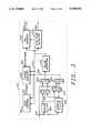
- FIG. 1shows a block diagram of the environment of the invention and illustrates the read channel that contains the invention
- FIG. 2shows a block diagram of the analog and analog to digital conversion circuitry of the read channel containing the invention
- FIG. 3shows a block diagram of the digital circuitry of the read channel containing the invention
- FIG. 4shows a signal waveform and illustrates center sampling of the pulses
- FIG. 5shows a signal waveform and illustrates side sampling of the pulses
- FIGS. 6 and 7show signal waveforms to illustrate overlapping pulses
- FIG. 8shows a block diagram of the timing recovery circuit of FIG. 3
- FIGS. 9-10show a logic block diagram of the acquisition circuit of the phase and frequency detector of FIG. 8;
- FIGS. 11-12show a logic block diagram of the tracking circuit of the phase and frequency detector of FIG. 8.
- FIG. 13shows a diagram of the loop filter circuit of the timing recovery block of FIG. 3.
- FIG. 1shows a block diagram of a typical environment of the invention.
- a computer system 100contains a processing element 102 which communicates to other elements of the computer system 100 over a system bus 104.
- a keyboard 106 and a display 108allow a user of the computer system 100 to communicate with the computer system 100.
- a memory 110contains programs and data which cause the computer system 100 to perform operations desired by the user.
- a disk data storage system 112is connected to the system bus 104 for storing data and programs within the computer system 100.
- a disk controller 114 within the disk device 112communicates to the system bus 104 and controls the operations of a disk drive 118, possibly in conjunction with a local microprocessor (not shown) within the disk data storage system 112.
- the disk drive 118performs the storage function, typically storing the data on magnetic media.
- a bus 116connects the disk controller 114 to the disk drive 118, specifically connecting to a write channel 120 to write data onto the disk through write heads and amplifiers 128. When data is being read from the disk through the read head and amplifiers 128 the data comes back through the read channel 122 which contains the timing recovery circuit of the present invention.
- the read and write headsmay be physically the same heads.
- the datafirst passes through the analog section 126 of the read channel 122 and then through the digital section 124 of the read channel 122 before being sent on the bus 116 to the disk controller 114. After being processed by the disk controller 114, the data is then sent over the system bus 104 to the memory 110 and/or the processing element 102.
- the disk controller 114also connects to other circuits, not shown, within the disk drive 118, such as a circuit which moves the read/write heads over the surface of the data storage media.
- the digital timing circuit of the present inventioncan be used for synchronizing a clock to pulses within data received from a transmission line, such as a telephone line or local area network, in a data communications receiver. It may also be used in any other device that must time and detect pulses within a signal.
- FIG. 2shows a block diagram of the analog circuitry 126 of the read channel 122.
- a read headwhen a read head is passing over a track of the data storage medium, it picks up a signal which is amplified by a preamplifier, not shown. After this preamplification, the signal 201 is passed to a variable gain amplifier 202. The signal is further amplified by the variable gain amplifier 202 and passed through an analog multiplexer 203 and then to an analog equalizer circuit 204, which filters the signal as desired, for example, so as to remove unwanted high frequencies and shape the remaining spectrum, to an Analog to Digital (A to D) converter 206.
- a to DAnalog to Digital
- the A to D converter 206converts the analog signal into a sequence of digital values, providing six bits of digital information per sample in the preferred embodiment, and then the data is passed to a register/de-multiplexer 207.
- the digital section 124 of the read channel 122processes two samples in parallel.
- the register/de-multiplexer 207stores every other sample taken by the A to D converter 206.
- the data from the two samplesis passed to the data bus 230.
- the bus 230is clocked by a single half-frequency clock signal.
- the timing necessary for converting the data, also called taking a sample, in the A to D converter 206is supplied by a variable frequency oscillator 222 which is controlled by the output of a digital to analog converter (DAC) 220.
- the input to the DAC 220comes from the digital section of the read channel 124 as timing feedback signal 234.
- the DAC 220may be an integral part of the variable frequency oscillator in such a way that the digital input controls the frequency directly.
- a reference signal 236is created by a frequency synthesizer 240 running at the frequency used for writing data, and dividing this frequency by four in the divide by four circuit 238.
- the output of the divide by four circuit 238is a square wave with period 4T which is connected to the analog multiplexer 203.
- the filter 204passes the fundamental frequency of the square wave but rejects the higher harmonics, thus converting the reference signal into a sinusoid with frequency 1/4T.
- This sinusoidal reference signalis equivalent to the data signal typically produced by alternating transitions and spaces, i.e. 101010... in NRZI representation. It is often called a "2T" pattern because the distance between transitions is 2 bit cells.
- the 2T patternis a pulse pattern often used for a preamble signal at the start of a data record.
- the reference pattern signal 236is used to set the VFO 222 to a nominal frequency before locking to data preamble.
- the gain of the variable gain amplifier 202is controlled through a gain feedback signal 232 which originates in the digital portion 124 of the read channel 122.
- the gain feedback signal 232is input to a summing junction 210 which has a coarse gain control value as its other input.
- the coarse gain controlcan be set by the disk controller 114, or a local microprocessor (not shown) within the disk drive, to provide a nominal gain level which is then adjusted up or down by the gain feedback signal 232.
- the feedback signalis sent to a digital to analog converter 212 and then to a filter 214. Because of the nature of many digital to analog converters, the output of the DAC 212 may contain glitches when it is changing values.
- the filter 214may be necessary to remove these glitches in the feedback signal.
- the signalis exponentiated by the exponential converter block 216 and then connected to the variable gain amplifier 202. This conversion makes the small-signal gain control dynamics independent of the input signal amplitude.
- FIG. 3shows a block diagram of the digital section 124 of the read channel 122 (FIG. 1).
- the digital data signal 230 from FIG. 2is input to a delay circuit 304 and a digital filter circuit 302.
- the outputs of these two circuitsare connected to multiplexers 306 and 316, whose outputs are connected to multiplexers 310 and 318 respectively.
- Multiplexers 310 and 318also receive signal 230.
- Multiplexers 306 and 316may be selected independently, however, multiplexers 310 and 318 are always selected together. In this manner, either the digital data signal 230 or the filtered/delayed signals may be selected for input to both a pulse detector 312 and a timing recovery circuit 328.
- the filter 302inserts a delay into the digital data signal 230, so if one circuit selects the filtered signal, the other circuit input must be delay compensated by selecting the delayed signal from circuit 304 or by also selecting the filtered signal from filter 302.
- the output of the pulse detector 312is connected to a gain control circuit 330 which provides the gain feedback signal 232 that connects to FIG. 2.
- the output of the pulse detector 312is also connected to the timing recovery circuit 328 whose output 234 connects to the digital to analog converter 220 of FIG. 2.
- the output of the pulse detector 312may also be connected to a sync mark detector 322 and an RLL decoder 320, as shown in FIG. 3, or a more sophisticated data detector (not shown) may be connected to the sync mark detector 322 and the RLL decoder 320.
- the output of the RLL decoder 320 and the sync mark detector 322are connected to the disk controller 114 (FIG. 1) through the bus 116.
- the pulse detector 312 and the timing recovery circuit 328are designed to process pulses using one of two types of sampling methods, selected by the user.
- the first sampling methodis called center sampling wherein one of the samples taken will arrive at or near the center, or peak, of a pulse as shown in FIG. 4.
- the location of the samplingis controlled by the timing recovery block 328.
- the timing recovery block 328will adjust the timing of the VFO 222 (FIG. 2) such that two consecutive samples are taken wherein one of the two samples appears on one side of the peak of the pulse and the other of the two samples appears on the other side of the peak as shown in FIG. 5.
- the user of the systemdetermines whether center sampling or side sampling is used by setting a bit in a control register through the interface 116 (FIG. 1).
- samplingcan occur during two different time segments within a data record being read from the disk media.
- the first time segment sampling occursis called acquisition mode, because it occurs when the gain control and timing control are acquiring the gain and timing relationships of the pulses. This occurs when the read head is passing a preamble portion of the data record which always has a known data pattern to facilitate acquisition of the timing and gain.
- acquisition modea different mode is used for the pulse detector and timing recovery, called tracking, since data has an irregular and a priori unknown pattern of pulses.
- the pulse detector and timing recovery circuitsare designed to process pulses under four separate conditions.
- the first conditionis acquisition mode using side sampling
- the secondis acquisition mode using center sampling
- thirdis tracking mode using side sampling
- fourthis tracking mode using center sampling.
- the timing recovery circuitanalyzes the current sample of the amplitude of the signal as well as the previous two samples of the signal amplitude. Using these three samples, Table 1 shows equations for the timing recovery circuit 328.
- nis the time of the current sample
- n-1is the first previous sample
- n-2is the second previous sample
- n-3is the third previous sample.
- y xis the sample value for a sample taken at time x.
- SGNis the arithmetic sign of the sample value.
- P xhas a value of 1 if a pulse is detected during sample x
- P xhas a value of 0 is a pulse is not detected during sample x.
- t ais the acquisition timing set point
- t tis the tracking timing set point.
- a, b, and care constants used to adjust for nearby pulses. The equations of Table 1 will be further described below.
- the equations of Table 1assume pulse detection at time n of a pulse whose peak occurs at time y n-1 for center sampling, or between y n-1 and y n-2 for side sampling.
- the circuits of FIGS. 9-12processes two signal samples simultaneously.
- the equations for the second sampleare the same as the equations of Table 1, with one time delay.
- y n in Table 1would be replaced by y n-1
- y n-1would be replaced by y n-2
- y n-2would be replaced by y n-3 .
- FIG. 4shows a signal waveform of an isolated pulse and illustrates center sampling of the pulse.
- a signal waveform 402is shown having four samples taken with the sample identified by reference 412, at time n, being the most recent sample.
- Sample 410, at time n-1is the sample just prior to the most recent sample, sample 408 is the next previous sample and sample 406 is the oldest of the four samples shown.
- Negative pulseswould appear as a mirror image of FIG. 4.
- the samples taken of the pulseare also identified as "a”, "b”, "1", and "c”.
- sample “a”occurs at time n-3 of each pulse
- sample “b”occurs at time n-2 of each pulse
- sample "1”occurs at time n-1 of each pulse
- sample “c”occurs at time n of each pulse.
- the sample labeled “1”is so labeled because the gain circuit adjusts the level of this sample to a nominal value of 1.
- FIG. 5shows a signal waveform of an isolated pulse and illustrates side sampling of the pulse.
- a signal waveform 502is shown as a positive level above a baseline 503.
- Four samplesare shown, with the most recent sample being sample 510.
- Sample 508is the sample previous to the most recent, 506 is the next previous sample and sample 504 is the oldest of the four samples shown. These samples are also identified by the time references n through n-3.
- FIGS. 6 and 7show waveforms and sample times for a typical pulse for side and center sampling, respectively and will be used to illustrate the equations shown in Table 1.
- a waveform 602is shown with side sampling mode, with the four samples of the waveforms, "a”, “b”, “1” and “c” being identified for the value of the waveform at sample times n-3, n-2, n-1, and n, respectively.
- pulsescan never occur at two successive sampling times, thus pulses must be separated by at least two sample times. Therefore, the pulse illustrated by dashed line 604 is the closest a pulse could occur prior to the pulse 602 and the pulse identified by dashed line 606 is the earliest another pulse could occur after the pulse 602.
- phase errorwill give the phase error for a symmetric isolated pulse. This phase error will be zero if the peak of the pulse occurs exactly at the center between the "b" and “1" samples, and will be non-zero if the peak is offset from the center. If the peak is offset left of center, the "b" sample value will be higher than the "1" sample value, resulting in a positive phase error value, and if the peak is offset right of center, the "b" sample value will be lower than the "1" sample value, resulting in a negative phase error value.
- pulse 604Since pulse 604 might have occurred two sample times earlier than pulse 602, the effects of this pulse must be considered in the equations.
- Sample “c” of pulse 604occurs at the same time as sample “b” of pulse 602. Therefore, if there was a peak detected at time n-2, i.e. p n-2 is one, the phase error is corrected by adding a constant value c to offset the "c" sample of pulse 604. This constant value is determined by calibration of the device and is input to the circuit through the interface 116 (FIG. 1).
- a pulsecould occur two sample times after pulse 602, represented in FIG. 6 by pulse 606.
- the "a" sampleoccurs at the same time as the "1" sample of pulse 602. Therefore, the phase error is corrected by subtracting a constant "a” if there is a pulse at time n+2, i.e. if p n+2 is one. This constant value is also determined by calibration of the device and input to the circuit through the interface 116 (FIG. 1).
- the equation for side sample acquisition modeis similar to the side sample tracking mode equation, except that the corrections for the pulses 604 and 606 need not occur. These corrections are unnecessary, because in acquisition mode the data pattern is known, since the same preamble is written before every data record. Therefore, the entire compensation for asymmetry and intersymbol interference can be accomplished with a single term t a .
- Table 2shows nominal values for t a for the three types of acquisition patterns used in the present invention. This constant value is also determined by calibration of the device and input to the circuit through the interface 116 (FIG. 1).
- FIG. 7shows waveforms when center sampling is being used.
- Table 1shows the center sampling equations, and the center sampled acquisition equation is very similar to side sampled acquisition equation, except that in center sampling the "b" and "c" samples of each pulse are used to determine phase error. Therefore, the center sampled acquisition equation substitutes y n for the y n-1 in the side sampled acquisition equation.
- the center sampled tracking equationincorporates the same kind of adjustments that were incorporated into the side sampled tracking equation, but the details differ.
- a pulse 704can overlap the pulse 702, and if this occurs, the "c" sample of pulse 704 overlaps the "b" sample of pulse 702. Therefore, the center sampled tracking equation adds the term "+c * p n-2 " to compensate for the pulse 704, where c is the same constant described for the side sampling equations.
- pulse 706can overlap pulse 702 and the center sampled tracking equation adds the term "-b * p n+2 " to compensate for the pulse 706, where b is a constant value determined by calibration of the device and input to the circuit through the interface 116 (FIG. 1).
- a third pulse, 708,can also overlap the pulse 702.
- One possible way to compensate for the pulse 708would be to subtract a constant "a" times p n+3 . However, this requires that the detector wait at least three sample times before determining the phase error for the pulse 702. As shown in FIG. 7, the value of the "a" sample for pulse 708 will typically be very small for center sampling. Because it is very small, this term of the equation can be deferred to a later clock cycle without much consequence. When deferred by three sample times, the correction "-a * p n+3 " may be included in the phase error equation for the next pulse (at time n+3), at which time it is included as "-a * P n-3 ". Therefore, the center sampled tracking equation includes the term "-a * p n-3 " to provide compensation for pulse 708.
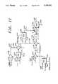
- FIG. 8shows a block diagram of the timing recovery circuit 328 of FIG. 3.
- the timing recovery circuit 328is shown having a phase/frequency detector 802 which is connected to a loop filter 808 to provide the timing feedback signal 234.
- the phase/frequency detector 802receives the output 314 of the pulse detector 312 (FIG. 3). As discussed above and shown in the equations of Table 1, this is the signal "P".
- the phase/frequency detector 802also receives the data samples 320 which may have been selected from the raw data samples 230 or after being delayed by the delay 304 or filtered by the digital filter 302.
- the phase/frequency detector 802receives an acquisition/tracking signal 810 which tells the phase/frequency detector 802 whether acquisition or tracking mode is being used.
- a read/lock signal 812tells the phase/frequency detector whether data is being read from the system, or whether the detector is in lock to reference mode.
- Lock to reference modeis used to set the frequency of the VFO 222 (FIG. 2) at a nominal frequency when data is not being read and thus minimize the initial frequency error when reading of data is started. This is accomplished by creating a periodic reference signal at a precisely controlled frequency equal to one fourth of the nominal sample rate. This signal is connected through analog multiplexer 203 (FIG. 2), into the normal data path. Thus, when not reading data, this reference signal may be used to set the VFO at the nominal frequency.
- Table 3shows the equation for the frequency detection, when the phase/frequency detector 802 is acting as a frequency detector. This equation is very similar to the center sampled acquisition phase error equation, except that the sign of y n is reversed and the t a term is absent. If the VFO 222 is sampling at the correct frequency, every other sample will have the same magnitude, but opposite in sign. Therefore, if the VFO 222 is sampling at the correct frequency, y n +y n-2 will be zero. if the VFO is low in frequency, the result is negative, and if the VFO is high, the result is positive.
- FIGS. 9-12show a logic block diagram of the circuit for the phase/frequency detector 802.
- FIGS. 9-10show the circuit for determining phase and frequency errors during acquisition mode
- FIGS. 11-12show the circuit for determining phase errors in tracking mode. Frequency errors are only determined during acquisition mode.
- two samplesare processed simultaneously.
- FIG. 9shows the processing of the first sample in acquisition mode
- FIG. 10shows the processing of the second sample in acquisition mode
- FIG. 10also combines the results of FIG. 9 and 10 for acquisition mode.
- FIG. 11shows the processing of the first sample in tracking mode
- FIG. 12shows processing of the second sample in tracking mode
- FIG. 11also combines the results of FIGS. 12 and 12 for tracking mode.
- circuits surrounded by dashed line 917partially solves the equations for side and center sampling acquisition mode and frequency detection to produce the result of:
- Multiplexer 912selects either y n or the inverted value of y n based on the sign of the data input y n+1 .
- Adder 914then adds this result to t a for phase error detection or zero for frequency detection, and delay circuit 916 delays the result by two time periods so that signal 918 becomes SGN (y n-1 ) * y n-2 +t a or SGN (y n-1 ) * y -2 +0.
- EXCLUSIVE OR circuit 927uses the sign bit, that is, bit five, of y n-1 and the READ/LOCK signal 812 to determine whether the output of multiplexer 928 should be inverted and a sign bit of one input to adder 934. If read mode is being used and the sign of y n-1 is positive, the output of multiplexer 928 is inverted and a sign bit of one is input to adder 934.
- FIG. 10performs the same function as FIG. 9 to produce a phase or frequency error signal 1036, however, it uses the previous sample as input, and then it combines the phase/frequency error outputs 936 of FIG. 9 and 1036 of FIG. 10.
- the previous sample inputs to multiplexer 1012are y n-1 rather than the y n inputs to multiplexer 912, as are the inputs to multiplexer 1028 and EXCLUSIVE OR circuit 1027.
- signal 1036is the phase/frequency error for the sample previous to the sample processed by FIG. 9.
- the NAND circuits 1038, 1040, and 1042combine the signals to produce the output 1044 which is sent to FIG. 12 to be combined with the tracking mode signals before being sent to the loop filter 808.
- the NAND circuits 1038, and 1040select either the output 936 from FIG. 9 or the output 1036 from FIG. 10 depending upon whether a pulse occurred at time n or at time n-1. These outputs are then connected to NAND circuit 1042 which produces the output 1044.
- FIGS. 11-12show the phase/frequency detector circuit for tracking mode.
- NAND circuit 1106provides the term "-a * p n-3 " for center sampling. For side sampling the output of NAND circuit 1106 is zero.
- Multiplexer 1114selects "t t +c * p n-2 " if a pulse occurred at time n-2 or "t t " alone if a pulse did not occur at time n-2. There are separate set points for acquisition mode and tracking mode.
- signal 1120represents "t t +c * p n-2 -a * p n-3 ", although the term "-a * p n-3 " will only be present for center sampling.
- Multiplexer 1124selects the value y n for center sampling and y n-1 for side sampling and inverts the value before sending it to adder 1122.
- a carry bit of oneis input to the adder 1122 through signal 1121 to cause either y n or y n-1 to be subtracted from y n-2 , signal 1020.
- EXCLUSIVE OR circuit 1126adjusts for the sign of y n-1 and adder 1128 combines the result with signal 1120 to produce the partial equation:
- Delay circuit 1130delays this result by two sample times and then adder circuit 1138 subtracts either the constant "a” for side sampling, or the constant "b” for center sampling, before sending the result to multiplexer 1140.
- Multiplexer 1140selects either the output of delay circuit 1130 or the output of adder circuit 1138 depending upon whether a peak occurred at time n. Since delay circuit 1130 has delayed the output of adder 1128 by two clock cycles, signal p n 1046 actually represents P n+2 and therefore determines whether the constant terms a or b should be added in. Therefore, output 1142 is the solution to the tracking equations of Table 1 for the current sample.
- FIG. 12is identical to the circuit of FIG. 11 except that the samples used are delayed by one, and additional circuitry exists to combine the two phase errors.
- the inputs to multiplexer 1224 and adder 1222are one sample behind the inputs to the equivalent circuits in FIG. 11 Therefore, the output 1242 provides the solution to the tracking equations of Table 1 delayed by one sample time.
- FIG. 12then combines the phase error results 1142 and 1242 of FIGS. 11 and 12, respectively, to provide the phase/frequency detector output 816 to the loop filter.
- the NAND circuits 1244 and 1248select the output 1142 of FIG. 11 or the output 1242 of FIG. 12 depending upon whether a pulse occurred at time n-2 or time n-3. This result is sent to NAND circuit 1246 which produces the output 1250 which is combined with the acquisition mode signals before being connected to the loop filter.
- NAND circuits 1260, 1262, and 1264select the acquisition phase/frequency error signal 1052 or the tracking phase error signal 1250, depending upon the TRK/ACQ signal to create the phase/frequency circuit output 816 which is sent to the loop filter.
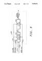
- FIG. 13shows a diagram of the loop filter 808.
- the z-domain transfer function of this filteris
- Coefficients c 1 1302 and c 2 1304are independently programmable for acquisition and tracking. For lock to reference mode, c 1 is set to zero and c 2 is independently programmable. A means is also provided to change the significance of the loop filter output between acquisition and tracking modes since the appropriate range and resolution of frequency control depends on which mode is used. Separate registers are provided for each mode to facilitate this change.
- Delay element 1306is used for pipelining and has little effect on the filter response.
- K pis the gain of the phase detector (which depends upon the pulse shape)
- K ois the control gain of the VCO
- nis the number of (2/f s ) clock delays in the loop.
Landscapes
- Engineering & Computer Science (AREA)
- Signal Processing (AREA)
- Power Engineering (AREA)
- Computer Networks & Wireless Communication (AREA)
- Signal Processing For Digital Recording And Reproducing (AREA)
- Stabilization Of Oscillater, Synchronisation, Frequency Synthesizers (AREA)
- Synchronisation In Digital Transmission Systems (AREA)
Abstract
Description
SGN (y.sub.n-1) * (y.sub.n-2 -y.sub.n-1)
SGN (y.sub.n-1) * (y.sub.n-2 -y.sub.n-1)+t.sub.t
SGN (y.sub.n-1) * y.sub.n-2 +t.sub.a
SGN (y.sub.n-1) * y.sub.n-2
-SGN (y.sub.n-1) * y.sub.n-1
-SGN (y.sub.n) * y.sub.n
+SGN (y.sub.n-1) * y.sub.n
SGN y.sub.n-1 * (y.sub.n-2 -y.sub.n)+t.sub.t +c * p.sub.n-2 -a * p.sub.n-3
F.sub.t (z)=(c.sub.1 * z * (z-1)+c.sub.2)/(z * (z-1))
G.sub.t (z)=(K.sub.p * K.sub.o * (c.sub.1 * z.sup.2 -c.sub.1 * z+c.sub.2)/(z.sup.n+1 * (z-1).sup.2)
TABLE 1 __________________________________________________________________________Acquisition Tracking __________________________________________________________________________Side SGN (Y.sub.n-1) * (Y.sub.n-2 - Y.sub.n-1) + t.sub.a SGN (Y.sub.n-1) * (Y.sub.n-2 - Y.sub.n-1) + t.sub.t + c*P.sub.n-2 - a*P.sub.n+2 Sampled Center SGN (Y.sub.n-1) * (Y.sub.n-2 - Y.sub.n) + t.sub.a SGN (Y.sub.n-1) * (Y.sub.n-2 - Y.sub.n) + t.sub.t + c*P.sub.n-2 - b*P.sub.n+2 - a*P.sub.n-3 Sampled __________________________________________________________________________
TABLE 2 ______________________________________ ACQUISITION PATTERN NOMINAL t.sub.a NOMINAL t.sub.t ______________________________________Side 1010 . . . 1 - b + c - a 1 - b Sampled 100100 . . . 1 - b 10001000 . . . 1 -b Center 1010 . . . 2 * (c - b) c - b Sampled 100100 . . . c - b + a 10001000 . . . c - b ______________________________________
TABLE 3 ______________________________________ Frequency Detector = SGN (Y.sub.n-1) * (Y.sub.n + Y.sub.n-2) ______________________________________
Claims (15)
Priority Applications (6)
| Application Number | Priority Date | Filing Date | Title |
|---|---|---|---|
| US07/954,350US5359631A (en) | 1992-09-30 | 1992-09-30 | Timing recovery circuit for synchronous waveform sampling |
| EP93922382AEP0663117B1 (en) | 1992-09-30 | 1993-09-24 | Timing recovery circuit for synchronous waveform sampling |
| DE69328432TDE69328432T2 (en) | 1992-09-30 | 1993-09-24 | CLOCK RECOVERY CIRCUIT FOR SYNCHRONOUS WAVEFORM SCAN |
| PCT/US1993/009110WO1994008394A1 (en) | 1992-09-30 | 1993-09-24 | Timing recovery circuit for synchronous waveform sampling |
| SG1996004699ASG46437A1 (en) | 1992-09-30 | 1993-09-24 | Timing recovery circuit for synchronous waveform sampling |
| JP6509196AJP2952042B2 (en) | 1992-09-30 | 1993-09-24 | Timing recovery circuit for synchronous waveform sampling |
Applications Claiming Priority (1)
| Application Number | Priority Date | Filing Date | Title |
|---|---|---|---|
| US07/954,350US5359631A (en) | 1992-09-30 | 1992-09-30 | Timing recovery circuit for synchronous waveform sampling |
Publications (1)
| Publication Number | Publication Date |
|---|---|
| US5359631Atrue US5359631A (en) | 1994-10-25 |
Family
ID=25495302
Family Applications (1)
| Application Number | Title | Priority Date | Filing Date |
|---|---|---|---|
| US07/954,350Expired - LifetimeUS5359631A (en) | 1992-09-30 | 1992-09-30 | Timing recovery circuit for synchronous waveform sampling |
Country Status (6)
| Country | Link |
|---|---|
| US (1) | US5359631A (en) |
| EP (1) | EP0663117B1 (en) |
| JP (1) | JP2952042B2 (en) |
| DE (1) | DE69328432T2 (en) |
| SG (1) | SG46437A1 (en) |
| WO (1) | WO1994008394A1 (en) |
Cited By (36)
| Publication number | Priority date | Publication date | Assignee | Title |
|---|---|---|---|---|
| US5572558A (en)* | 1994-11-17 | 1996-11-05 | Cirrus Logic, Inc. | PID loop filter for timing recovery in a sampled amplitude read channel |
| US5585975A (en)* | 1994-11-17 | 1996-12-17 | Cirrus Logic, Inc. | Equalization for sample value estimation and sequence detection in a sampled amplitude read channel |
| EP0769781A2 (en) | 1995-10-20 | 1997-04-23 | Cirrus Logic, Inc. | Cost reduced interpolated timing recovery in a sampled amplitude read channel |
| EP0777211A2 (en) | 1995-12-05 | 1997-06-04 | Cirrus Logic, Inc. | A magnetic disk sampled amplitude read channel employing interpolated timing recovery for synchronous detection of embedded servo data |
| US5642243A (en)* | 1994-09-27 | 1997-06-24 | Cirrus Logic, Inc. | Timing recovery frequency error detector for sampled amplitude magnetic recording |
| US5668678A (en)* | 1994-11-14 | 1997-09-16 | Cirrus Logic, Inc. | Detecting servo data and servo bursts from discrete time samples of an analog read signal in a sampled amplitude read channel |
| US5696639A (en)* | 1995-05-12 | 1997-12-09 | Cirrus Logic, Inc. | Sampled amplitude read channel employing interpolated timing recovery |
| US5717619A (en)* | 1995-10-20 | 1998-02-10 | Cirrus Logic, Inc. | Cost reduced time varying fir filter |
| US5786950A (en)* | 1996-07-29 | 1998-07-28 | Cirrus Logic, Inc. | PR4 sampled amplitude read channel employing an NRZI write modulator and a PR4/NRZI converter |
| US5796535A (en)* | 1995-05-12 | 1998-08-18 | Cirrus Logic, Inc. | Sampled amplitude read channel employing a user data frequency synthesizer and a servo data frequency synthesizer |
| US5802118A (en)* | 1996-07-29 | 1998-09-01 | Cirrus Logic, Inc. | Sub-sampled discrete time read channel for computer storage systems |
| US5808573A (en)* | 1996-08-01 | 1998-09-15 | Nec Electronics Incorporated | Methods and structure for sampled-data timing recovery with reduced complexity and latency |
| US5812336A (en)* | 1995-12-05 | 1998-09-22 | Cirrus Logic, Inc. | Fixed sample rate sampled amplitude read channel for zoned magnetic recording |
| US5812334A (en)* | 1993-02-01 | 1998-09-22 | Cirrus Logic, Inc. | Synchronous read channel employing discrete timing recovery, transition detector, and sequence detector |
| US5825211A (en)* | 1995-09-29 | 1998-10-20 | Dallas Semiconductor Corporation | Oversampled state machine for jitter tolerant pulse detection |
| US5838738A (en)* | 1996-07-29 | 1998-11-17 | Cirrus Logic, Inc. | Coding to improve timing recovery in a sampled amplitude read channel |
| US5914989A (en)* | 1997-02-19 | 1999-06-22 | Nec Electronics, Inc. | PRML system with reduced complexity maximum likelihood detector |
| FR2775143A1 (en)* | 1998-02-18 | 1999-08-20 | Atg Sa | Method for automatic correction of gain of clock phase servo loop in optical disc reader/recorder |
| US5949820A (en)* | 1996-08-01 | 1999-09-07 | Nec Electronics Inc. | Method for optimizing an equalization and receive filter |
| US5999355A (en)* | 1996-04-30 | 1999-12-07 | Cirrus Logic, Inc. | Gain and phase constrained adaptive equalizing filter in a sampled amplitude read channel for magnetic recording |
| US6032284A (en)* | 1997-03-12 | 2000-02-29 | Cirrus Logic, Inc. | Trellis coding system for disc storage systems |
| US6246723B1 (en) | 1998-05-04 | 2001-06-12 | Cirrus Logic, Inc. | Sampled amplitude read channel employing early-decisions from a trellis sequence detector for sampling value estimation |
| US6452736B1 (en)* | 1994-05-26 | 2002-09-17 | Hitachi, Ltd. | Magnetic recording and reproducing apparatus and a read/write amplifier having a signal transmission system with high speed of data write signal |
| US20030026369A1 (en)* | 2001-08-02 | 2003-02-06 | Murray Carl Damien | Timing recovery in data communication circuits |
| US20030066023A1 (en)* | 2001-08-10 | 2003-04-03 | Samsung Electronics Co., Ltd | Asymmetric error correction apparatus and method, and clock recovering apparatus for optical reading system employing the same |
| EP1126616A3 (en)* | 2000-02-14 | 2003-11-12 | STMicroelectronics, Inc. | Circuit and method for determining the phase difference between a sample clock and a sampled signal |
| US6819514B1 (en) | 1996-04-30 | 2004-11-16 | Cirrus Logic, Inc. | Adaptive equalization and interpolated timing recovery in a sampled amplitude read channel for magnetic recording |
| US6823133B1 (en) | 1999-11-15 | 2004-11-23 | Lexmark International, Inc. | Apparatus and method for electronic control of DC motor using an all-digital phase-locked loop |
| US20050094301A1 (en)* | 2003-10-31 | 2005-05-05 | International Business Machines Corporation | Magnetic recording channel utilizing control fields for timing recovery, equalization, amplitude and amplitude asymmetry |
| US20050135465A1 (en)* | 2003-12-19 | 2005-06-23 | Andrus Jeremy C. | Device with improved serial communication |
| US20050190474A1 (en)* | 2004-02-26 | 2005-09-01 | Hitachi Global Technologies Netherlands B.V. | Method and apparatus for providing write pre-compensation using a read timing path |
| US7002764B2 (en) | 2004-02-26 | 2006-02-21 | Hitachi Global Storage Technologies Netherlands B.V. | Method and apparatus for providing generalized write pre-compensation |
| US7136440B2 (en)* | 1997-12-22 | 2006-11-14 | Stmicroelectronics, Inc. | Timing recovery for data sampling of a detector |
| US20070177292A1 (en)* | 2006-02-01 | 2007-08-02 | Bui Nhan X | Using at least one servo channel to provide timing recovery and timing information to data channels |
| CN100423120C (en)* | 2002-04-23 | 2008-10-01 | 皇家飞利浦电子股份有限公司 | Interference-free lms-based adaptive asynchronous receiver |
| US7920601B2 (en) | 2003-12-19 | 2011-04-05 | Gentex Corporation | Vehicular communications system having improved serial communication |
Families Citing this family (4)
| Publication number | Priority date | Publication date | Assignee | Title |
|---|---|---|---|---|
| US5504790A (en)* | 1994-12-09 | 1996-04-02 | Conner Peripherals, Inc. | Digital data phase detector |
| WO1996018192A1 (en)* | 1994-12-09 | 1996-06-13 | Seagate Technology, Inc. | Apparatus and method for controlling the frequency at which data is written in a disk drive system |
| US5793548A (en)* | 1995-05-12 | 1998-08-11 | Cirrus Logic, Inc. | Fault tolerant sync mark detector for comparing a sign and magnitude of a detected sequence to a target sync mark in sampled amplitude magnetic recording |
| CN111010169B (en)* | 2018-10-08 | 2024-01-19 | 中兴通讯股份有限公司 | Phase detection method, device, storage medium and electronic device |
Citations (5)
| Publication number | Priority date | Publication date | Assignee | Title |
|---|---|---|---|---|
| US4416017A (en)* | 1981-01-05 | 1983-11-15 | Motorola, Inc. | Apparatus and method for attenuating interfering signals |
| US4609907A (en)* | 1984-10-31 | 1986-09-02 | International Business Machines Corporation | Dual channel partial response system |
| US4890299A (en)* | 1987-11-13 | 1989-12-26 | International Business Machines Corporation | Fast timing acquisition for partial-response signalling |
| US5068628A (en)* | 1990-11-13 | 1991-11-26 | Level One Communications, Inc. | Digitally controlled timing recovery loop |
| US5216554A (en)* | 1991-07-01 | 1993-06-01 | International Business Machines Corporation | Digital phase error estimator |
Family Cites Families (1)
| Publication number | Priority date | Publication date | Assignee | Title |
|---|---|---|---|---|
| JP2978621B2 (en)* | 1992-02-18 | 1999-11-15 | 日本電気アイシーマイコンシステム株式会社 | Digital PLL circuit |
- 1992
- 1992-09-30USUS07/954,350patent/US5359631A/ennot_activeExpired - Lifetime
- 1993
- 1993-09-24DEDE69328432Tpatent/DE69328432T2/ennot_activeExpired - Lifetime
- 1993-09-24EPEP93922382Apatent/EP0663117B1/ennot_activeExpired - Lifetime
- 1993-09-24SGSG1996004699Apatent/SG46437A1/enunknown
- 1993-09-24WOPCT/US1993/009110patent/WO1994008394A1/enactiveIP Right Grant
- 1993-09-24JPJP6509196Apatent/JP2952042B2/ennot_activeExpired - Fee Related
Patent Citations (5)
| Publication number | Priority date | Publication date | Assignee | Title |
|---|---|---|---|---|
| US4416017A (en)* | 1981-01-05 | 1983-11-15 | Motorola, Inc. | Apparatus and method for attenuating interfering signals |
| US4609907A (en)* | 1984-10-31 | 1986-09-02 | International Business Machines Corporation | Dual channel partial response system |
| US4890299A (en)* | 1987-11-13 | 1989-12-26 | International Business Machines Corporation | Fast timing acquisition for partial-response signalling |
| US5068628A (en)* | 1990-11-13 | 1991-11-26 | Level One Communications, Inc. | Digitally controlled timing recovery loop |
| US5216554A (en)* | 1991-07-01 | 1993-06-01 | International Business Machines Corporation | Digital phase error estimator |
Non-Patent Citations (20)
| Title |
|---|
| Abbott, W. L. and Cioffi, J. M., "Timing Recovery for Adaptive Decision Feedback Equalization of the Magnetic Storage Channel", Proceedings of IEEE Global Telecommunications Conference (Globecom), San Diego, Calif., 1990. |
| Abbott, W. L. and Cioffi, J. M., Timing Recovery for Adaptive Decision Feedback Equalization of the Magnetic Storage Channel , Proceedings of IEEE Global Telecommunications Conference (Globecom), San Diego, Calif., 1990.* |
| Cideciyan, R., Dolivo, F., Hermann, R., Hirt, W., Schott, W., "A PRML System for Digital Magnetic Recording", IEEE, Log Number 9104232, 1992. |
| Cideciyan, R., Dolivo, F., Hermann, R., Hirt, W., Schott, W., A PRML System for Digital Magnetic Recording , IEEE, Log Number 9104232, 1992.* |
| Dolivo, F., Schott, W., Ungerb ck, G. Fast Timing Recovery for Partial Response Signaling Systems , Published in the Proceedings of the 1989 ICC Conference (IEEE).* |
| Dolivo, F., Schott, W., Ungerbock, G. "Fast Timing Recovery for Partial-Response Signaling Systems", Published in the Proceedings of the 1989 ICC Conference (IEEE). |
| Fagan, A. D. and O Connor, R. E., Measurements on the Timing Recovery Performance of Partial Response Class 4 Signalling , IEEE Proceedings, vol. 136, 4, pp. 254 258, Aug. 1989.* |
| Fagan, A. D. and O'Connor, R. E., "Measurements on the Timing Recovery Performance of Partial-Response Class-4 Signalling", IEEE Proceedings, vol. 136, #4, pp. 254-258, Aug. 1989. |
| Jennings, A. and Clarke, B. R., "Data-Sequence Selective Timing Recovery for PAM Systems", IEEE Transactions on Communications, vol. Com-33, #7, pp. 729-731, Jul. 1985. |
| Jennings, A. and Clarke, B. R., Data Sequence Selective Timing Recovery for PAM Systems , IEEE Transactions on Communications, vol. Com 33, 7, pp. 729 731, Jul. 1985.* |
| Lee, E. A. and Messerschmitt, D. G., "Timing Recovery", Digital Communication, Kluwer Academic Publishers, Boston, 1988, Chapter 15, pp. 560-586. |
| Lee, E. A. and Messerschmitt, D. G., Timing Recovery , Digital Communication, Kluwer Academic Publishers, Boston, 1988, Chapter 15, pp. 560 586.* |
| Lyon, D. L., "Timing Recovery in Synchronous Equalized Data Communication", IEEE Transactions on Communications, pp. 269-274, Feb. 1975. |
| Lyon, D. L., Timing Recovery in Synchronous Equalized Data Communication , IEEE Transactions on Communications, pp. 269 274, Feb. 1975.* |
| Mueller, K. H. and M ller, M., Timing Recovery in Digital Synchronous Data Receivers , IEEE Transactions on Communications, vol. Com 24, No. 5, pp. 516 531, May 1976.* |
| Mueller, K. H. and Muller, M., "Timing Recovery in Digital Synchronous Data Receivers", IEEE Transactions on Communications, vol. Com-24, No. 5, pp. 516-531, May 1976. |
| Qureshi, Shahid U. H., "Timing Recovery for Equalized Partial-Response Systems", IEEE Transactions on Communications, pp. 1326-1331, Dec. 1976. |
| Qureshi, Shahid U. H., Timing Recovery for Equalized Partial Response Systems , IEEE Transactions on Communications, pp. 1326 1331, Dec. 1976.* |
| Saltzberg, B. R., "Timing Recovery for Synchronous Binary Data Transmission", The Bell System Technical Journal, pp. 593-622, Mar. 1967. |
| Saltzberg, B. R., Timing Recovery for Synchronous Binary Data Transmission , The Bell System Technical Journal, pp. 593 622, Mar. 1967.* |
Cited By (70)
| Publication number | Priority date | Publication date | Assignee | Title |
|---|---|---|---|---|
| US5991107A (en)* | 1993-02-01 | 1999-11-23 | Cirrus Logic, Inc. | Sychronous read channel |
| US5867331A (en)* | 1993-02-01 | 1999-02-02 | Cirrus Logic, Inc. | Synchronous read channel processing more than one channel sample at a time to increase throughput |
| US5966257A (en)* | 1993-02-01 | 1999-10-12 | Cirrus Logic, Inc. | Synchronous read channel integrated circuit employing discrete time timing recovery |
| US5812334A (en)* | 1993-02-01 | 1998-09-22 | Cirrus Logic, Inc. | Synchronous read channel employing discrete timing recovery, transition detector, and sequence detector |
| US5909331A (en)* | 1993-02-01 | 1999-06-01 | Cirrus Logic, Inc. | Synchronous read channel sintegrated circuit employing a fault tolerant sync mark detector and method for recovering an undetectable sync mark |
| US5844738A (en)* | 1993-02-01 | 1998-12-01 | Cirrus Logic, Inc. | Synchronous read channel employing a sequence detector with programmable detector levels |
| US5978162A (en)* | 1993-02-01 | 1999-11-02 | Cirrus Logic, Inc. | Synchronous read channel integrated circuit employing a channel quality circuit for calibration |
| US5917668A (en)* | 1993-02-01 | 1999-06-29 | Cirrus Logic, Inc. | Synchronous read channel employing a frequency synthesizer for locking a timing recovery phase-lock loop to a reference frequency |
| US5844509A (en)* | 1993-02-01 | 1998-12-01 | Cirrus Logic, Inc. | Synchronous read channel employing a data randomizer |
| US6021011A (en)* | 1993-02-01 | 2000-02-01 | Cirrus Logic, Inc. | Synchronous read channel employing a digital center frequency setting for a variable frequency oscillator in discrete time timing recovery |
| US6700721B2 (en) | 1994-05-26 | 2004-03-02 | Hitachi, Ltd. | Magnetic recording and reproducing apparatus and semiconductor integrated circuit for use in the same comprising a read/write signal processor having an interleave write data generator |
| US6452736B1 (en)* | 1994-05-26 | 2002-09-17 | Hitachi, Ltd. | Magnetic recording and reproducing apparatus and a read/write amplifier having a signal transmission system with high speed of data write signal |
| US5642243A (en)* | 1994-09-27 | 1997-06-24 | Cirrus Logic, Inc. | Timing recovery frequency error detector for sampled amplitude magnetic recording |
| US5754352A (en)* | 1994-09-27 | 1998-05-19 | Cirrus Logic, Inc. | Synchronous read channel employing an expected sample value generator for acquiring a preamble |
| US6144513A (en)* | 1994-11-14 | 2000-11-07 | Cirrus Logic, Inc. | Detecting servo data and servo bursts from discrete time samples of an analog read signal in a sampled amplitude read channel |
| US5668678A (en)* | 1994-11-14 | 1997-09-16 | Cirrus Logic, Inc. | Detecting servo data and servo bursts from discrete time samples of an analog read signal in a sampled amplitude read channel |
| US5854714A (en)* | 1994-11-14 | 1998-12-29 | Cirrus Logic, Inc. | Digital servo demodulation for sampled amplitude magnetic recording |
| US5572558A (en)* | 1994-11-17 | 1996-11-05 | Cirrus Logic, Inc. | PID loop filter for timing recovery in a sampled amplitude read channel |
| US5585975A (en)* | 1994-11-17 | 1996-12-17 | Cirrus Logic, Inc. | Equalization for sample value estimation and sequence detection in a sampled amplitude read channel |
| US5966258A (en)* | 1995-05-12 | 1999-10-12 | Cirrus Logic, Inc. | Asynchronous/synchronous digital gain control loop in a sampled amplitude read channel |
| US5796535A (en)* | 1995-05-12 | 1998-08-18 | Cirrus Logic, Inc. | Sampled amplitude read channel employing a user data frequency synthesizer and a servo data frequency synthesizer |
| US6108151A (en)* | 1995-05-12 | 2000-08-22 | Cirrus Logic, Inc. | Sampled amplitude read channel for reading user data and embedded servo data from a magnetic medium |
| US5696639A (en)* | 1995-05-12 | 1997-12-09 | Cirrus Logic, Inc. | Sampled amplitude read channel employing interpolated timing recovery |
| US6646822B1 (en) | 1995-05-12 | 2003-11-11 | Cirrus Logic, Inc. | Sampled amplitude read channel employing pipelined reads to reduce the gap between sectors |
| US5909332A (en)* | 1995-05-12 | 1999-06-01 | Cirrus Logic, Inc. | Sampled amplitude read channel employing interpolated timing recovery |
| US5825211A (en)* | 1995-09-29 | 1998-10-20 | Dallas Semiconductor Corporation | Oversampled state machine for jitter tolerant pulse detection |
| US6002274A (en)* | 1995-09-29 | 1999-12-14 | Dallas Semiconductor | Oversampled state machine for jitter tolerant pulse detection |
| EP0769781A2 (en) | 1995-10-20 | 1997-04-23 | Cirrus Logic, Inc. | Cost reduced interpolated timing recovery in a sampled amplitude read channel |
| US5717619A (en)* | 1995-10-20 | 1998-02-10 | Cirrus Logic, Inc. | Cost reduced time varying fir filter |
| EP0769781A3 (en)* | 1995-10-20 | 1998-05-20 | Cirrus Logic, Inc. | Cost reduced interpolated timing recovery in a sampled amplitude read channel |
| US5760984A (en)* | 1995-10-20 | 1998-06-02 | Cirrus Logic, Inc. | Cost reduced interpolated timing recovery in a sampled amplitude read channel |
| EP0777211A2 (en) | 1995-12-05 | 1997-06-04 | Cirrus Logic, Inc. | A magnetic disk sampled amplitude read channel employing interpolated timing recovery for synchronous detection of embedded servo data |
| US5812336A (en)* | 1995-12-05 | 1998-09-22 | Cirrus Logic, Inc. | Fixed sample rate sampled amplitude read channel for zoned magnetic recording |
| JP3164519B2 (en) | 1995-12-05 | 2001-05-08 | シーラス ロジック,インコーポレイテッド | Sample amplitude read channel for reading embedded servo data and method therefor |
| US5726818A (en)* | 1995-12-05 | 1998-03-10 | Cirrus Logic, Inc. | Magnetic disk sampled amplitude read channel employing interpolated timing recovery for synchronous detection of embedded servo data |
| US6208481B1 (en) | 1996-04-30 | 2001-03-27 | Cirrus Logic, Inc. | Gain and phase constrained adaptive equalizing filter in a sampled amplitude read channel for magnetic recording |
| US5999355A (en)* | 1996-04-30 | 1999-12-07 | Cirrus Logic, Inc. | Gain and phase constrained adaptive equalizing filter in a sampled amplitude read channel for magnetic recording |
| US6819514B1 (en) | 1996-04-30 | 2004-11-16 | Cirrus Logic, Inc. | Adaptive equalization and interpolated timing recovery in a sampled amplitude read channel for magnetic recording |
| US5802118A (en)* | 1996-07-29 | 1998-09-01 | Cirrus Logic, Inc. | Sub-sampled discrete time read channel for computer storage systems |
| US5786950A (en)* | 1996-07-29 | 1998-07-28 | Cirrus Logic, Inc. | PR4 sampled amplitude read channel employing an NRZI write modulator and a PR4/NRZI converter |
| US5838738A (en)* | 1996-07-29 | 1998-11-17 | Cirrus Logic, Inc. | Coding to improve timing recovery in a sampled amplitude read channel |
| US6154017A (en)* | 1996-08-01 | 2000-11-28 | Nec Electronics, Inc. | Temperature/voltage compensation circuit |
| US5949820A (en)* | 1996-08-01 | 1999-09-07 | Nec Electronics Inc. | Method for optimizing an equalization and receive filter |
| US5808573A (en)* | 1996-08-01 | 1998-09-15 | Nec Electronics Incorporated | Methods and structure for sampled-data timing recovery with reduced complexity and latency |
| US5914989A (en)* | 1997-02-19 | 1999-06-22 | Nec Electronics, Inc. | PRML system with reduced complexity maximum likelihood detector |
| US6032284A (en)* | 1997-03-12 | 2000-02-29 | Cirrus Logic, Inc. | Trellis coding system for disc storage systems |
| US7136440B2 (en)* | 1997-12-22 | 2006-11-14 | Stmicroelectronics, Inc. | Timing recovery for data sampling of a detector |
| WO1999043088A1 (en)* | 1998-02-18 | 1999-08-26 | Atg | Method for automatically correcting a phase servo loop gain |
| FR2775143A1 (en)* | 1998-02-18 | 1999-08-20 | Atg Sa | Method for automatic correction of gain of clock phase servo loop in optical disc reader/recorder |
| US6246723B1 (en) | 1998-05-04 | 2001-06-12 | Cirrus Logic, Inc. | Sampled amplitude read channel employing early-decisions from a trellis sequence detector for sampling value estimation |
| US6823133B1 (en) | 1999-11-15 | 2004-11-23 | Lexmark International, Inc. | Apparatus and method for electronic control of DC motor using an all-digital phase-locked loop |
| EP1126616A3 (en)* | 2000-02-14 | 2003-11-12 | STMicroelectronics, Inc. | Circuit and method for determining the phase difference between a sample clock and a sampled signal |
| US6775084B1 (en) | 2000-02-14 | 2004-08-10 | Stmicroelectronics, Inc. | Circuit and method for determining the phase difference between a sample clock and a sampled signal |
| US20030026369A1 (en)* | 2001-08-02 | 2003-02-06 | Murray Carl Damien | Timing recovery in data communication circuits |
| US7519137B2 (en)* | 2001-08-02 | 2009-04-14 | Agere Systems, Inc. | Timing recovery in data communication circuits |
| US20030066023A1 (en)* | 2001-08-10 | 2003-04-03 | Samsung Electronics Co., Ltd | Asymmetric error correction apparatus and method, and clock recovering apparatus for optical reading system employing the same |
| US6964007B2 (en)* | 2001-08-10 | 2005-11-08 | Samsung Electronics Co., Ltd. | Asymmetric error correction apparatus and method, and clock recovering apparatus for optical reading system employing the same |
| CN100423120C (en)* | 2002-04-23 | 2008-10-01 | 皇家飞利浦电子股份有限公司 | Interference-free lms-based adaptive asynchronous receiver |
| US20050094301A1 (en)* | 2003-10-31 | 2005-05-05 | International Business Machines Corporation | Magnetic recording channel utilizing control fields for timing recovery, equalization, amplitude and amplitude asymmetry |
| US7102839B2 (en) | 2003-10-31 | 2006-09-05 | International Business Machines Corporation | Magnetic recording channel utilizing control fields for timing recovery, equalization, amplitude and amplitude asymmetry |
| US20050135465A1 (en)* | 2003-12-19 | 2005-06-23 | Andrus Jeremy C. | Device with improved serial communication |
| US7920601B2 (en) | 2003-12-19 | 2011-04-05 | Gentex Corporation | Vehicular communications system having improved serial communication |
| US7405650B2 (en)* | 2003-12-19 | 2008-07-29 | Gentex Corporation | Device with improved serial communication |
| US20050190474A1 (en)* | 2004-02-26 | 2005-09-01 | Hitachi Global Technologies Netherlands B.V. | Method and apparatus for providing write pre-compensation using a read timing path |
| US7123429B2 (en) | 2004-02-26 | 2006-10-17 | Hitachi Global Storage Technologies Netherlands B.V. | Method and apparatus for providing write pre-compensation using a read timing path |
| US7123430B2 (en) | 2004-02-26 | 2006-10-17 | Hitachi Global Storage Technologies Netherlands B.V. | Method and apparatus for providing write pre-compensation using a read timing path |
| US7002764B2 (en) | 2004-02-26 | 2006-02-21 | Hitachi Global Storage Technologies Netherlands B.V. | Method and apparatus for providing generalized write pre-compensation |
| US20050200996A1 (en)* | 2004-02-26 | 2005-09-15 | Hitachi Global Storage Technologies Netherlands B.V. | Method and apparatus for providing write pre-compensation using a read timing path |
| US20070177292A1 (en)* | 2006-02-01 | 2007-08-02 | Bui Nhan X | Using at least one servo channel to provide timing recovery and timing information to data channels |
| US7433142B2 (en) | 2006-02-01 | 2008-10-07 | International Business Machines Corporation | Using at least one servo channel to provide timing recovery and timing information to data channels |
Also Published As
| Publication number | Publication date |
|---|---|
| EP0663117A4 (en) | 1995-11-02 |
| EP0663117B1 (en) | 2000-04-19 |
| EP0663117A1 (en) | 1995-07-19 |
| JPH08502393A (en) | 1996-03-12 |
| SG46437A1 (en) | 1998-02-20 |
| JP2952042B2 (en) | 1999-09-20 |
| DE69328432T2 (en) | 2000-09-14 |
| WO1994008394A1 (en) | 1994-04-14 |
| DE69328432D1 (en) | 2000-05-25 |
Similar Documents
| Publication | Publication Date | Title |
|---|---|---|
| US5359631A (en) | Timing recovery circuit for synchronous waveform sampling | |
| US5297184A (en) | Gain control circuit for synchronous waveform sampling | |
| US6111710A (en) | Asynchronous/synchronous gain control for interpolated timing recovery in a sampled amplitude read channel | |
| JP3164519B2 (en) | Sample amplitude read channel for reading embedded servo data and method therefor | |
| US5585975A (en) | Equalization for sample value estimation and sequence detection in a sampled amplitude read channel | |
| KR100469599B1 (en) | Gain- and Phase-Limited Adaptive Equalizer Filter in Magnetic Amplitude Reading Channels | |
| US5917668A (en) | Synchronous read channel employing a frequency synthesizer for locking a timing recovery phase-lock loop to a reference frequency | |
| KR100497916B1 (en) | Adaptive Equalization and Interpolated Time Recovery in Sample Amplification Readout Channels for Magnetic Recording | |
| US5937020A (en) | Digital information signal reproducing circuit and digital information system | |
| EP0455749B1 (en) | Read channel detector for use in digital magnetic recording systems | |
| KR20020006683A (en) | Digital recording/data reproducing apparatus | |
| US5748045A (en) | Digital PLL circuit | |
| US5272730A (en) | Digital phase-locked loop filter | |
| US5107379A (en) | Read channel detector with improved signaling speed | |
| US20060181975A1 (en) | Cross-talk cancellation scheme for rll-based storage systems | |
| EP0756744B1 (en) | Arrangement for reproducing n digital signals from n adjacent tracks on a record carrier | |
| JP2007179739A (en) | Sampled amplitude read channel | |
| US6097560A (en) | Reproducing apparatus having clock generator controlled by detected phase-difference and tendency of phase-difference | |
| US7193942B2 (en) | Phase difference correction apparatus and data reproduction apparatus including data header detection apparatus | |
| EP0530776B1 (en) | Timing recovering apparatus | |
| KR100289821B1 (en) | Data detector and method therefor | |
| JPH0793909A (en) | Phase detection circuit | |
| KR19980085436A (en) | Data reproducing device | |
| JPH0963206A (en) | Method for synchronizing identification clock in data reproducing apparatus and data reproducing apparatus | |
| JP2675739B2 (en) | Data demodulation circuit |
Legal Events
| Date | Code | Title | Description |
|---|---|---|---|
| AS | Assignment | Owner name:CIRRUS LOGIC, INC., CALIFORNIA Free format text:ASSIGNMENT OF ASSIGNORS INTEREST.;ASSIGNORS:BEHRENS, RICHARD T.;DUDLEY, TRENT;GLOVER, NEAL;REEL/FRAME:006369/0049 Effective date:19920929 | |
| AS | Assignment | Owner name:CIRRUS LOGIC, INC., CALIFORNIA Free format text:ASSIGNMENT OF ASSIGNORS INTEREST;ASSIGNOR:WELLAND, DAVID R.;REEL/FRAME:006997/0829 Effective date:19931206 | |
| STCF | Information on status: patent grant | Free format text:PATENTED CASE | |
| AS | Assignment | Owner name:BANK OF AMERICA NATIONAL TRUST & SAVINGS ASSOCIATI Free format text:SECURITY INTEREST;ASSIGNOR:CIRRUS LOGIC, INC.;REEL/FRAME:007986/0917 Effective date:19960430 | |
| FPAY | Fee payment | Year of fee payment:4 | |
| FEPP | Fee payment procedure | Free format text:PAYOR NUMBER ASSIGNED (ORIGINAL EVENT CODE: ASPN); ENTITY STATUS OF PATENT OWNER: LARGE ENTITY | |
| FPAY | Fee payment | Year of fee payment:8 | |
| REMI | Maintenance fee reminder mailed | ||
| AS | Assignment | Owner name:CIRRUS LOGIC INTERNATIONAL LTD., BERMUDA Free format text:DEED OF DISCHARGE;ASSIGNOR:BANK OF AMERICA NATIONAL TRUST SAVINGS ASSOCIATION;REEL/FRAME:013782/0435 Effective date:19970630 | |
| FPAY | Fee payment | Year of fee payment:12 |