US5359280A - Bilateral power converter for a satellite power system - Google Patents
Bilateral power converter for a satellite power systemDownload PDFInfo
- Publication number
- US5359280A US5359280AUS08/192,186US19218694AUS5359280AUS 5359280 AUS5359280 AUS 5359280AUS 19218694 AUS19218694 AUS 19218694AUS 5359280 AUS5359280 AUS 5359280A
- Authority
- US
- United States
- Prior art keywords
- signal
- terminal
- coupled
- power conversion
- output
- Prior art date
- Legal status (The legal status is an assumption and is not a legal conclusion. Google has not performed a legal analysis and makes no representation as to the accuracy of the status listed.)
- Expired - Fee Related
Links
Images


Classifications
- H—ELECTRICITY
- H02—GENERATION; CONVERSION OR DISTRIBUTION OF ELECTRIC POWER
- H02M—APPARATUS FOR CONVERSION BETWEEN AC AND AC, BETWEEN AC AND DC, OR BETWEEN DC AND DC, AND FOR USE WITH MAINS OR SIMILAR POWER SUPPLY SYSTEMS; CONVERSION OF DC OR AC INPUT POWER INTO SURGE OUTPUT POWER; CONTROL OR REGULATION THEREOF
- H02M3/00—Conversion of DC power input into DC power output
- H02M3/02—Conversion of DC power input into DC power output without intermediate conversion into AC
- H02M3/04—Conversion of DC power input into DC power output without intermediate conversion into AC by static converters
- H02M3/10—Conversion of DC power input into DC power output without intermediate conversion into AC by static converters using discharge tubes with control electrode or semiconductor devices with control electrode
- H02M3/145—Conversion of DC power input into DC power output without intermediate conversion into AC by static converters using discharge tubes with control electrode or semiconductor devices with control electrode using devices of a triode or transistor type requiring continuous application of a control signal
- H02M3/155—Conversion of DC power input into DC power output without intermediate conversion into AC by static converters using discharge tubes with control electrode or semiconductor devices with control electrode using devices of a triode or transistor type requiring continuous application of a control signal using semiconductor devices only
- H02M3/156—Conversion of DC power input into DC power output without intermediate conversion into AC by static converters using discharge tubes with control electrode or semiconductor devices with control electrode using devices of a triode or transistor type requiring continuous application of a control signal using semiconductor devices only with automatic control of output voltage or current, e.g. switching regulators
- H02M3/158—Conversion of DC power input into DC power output without intermediate conversion into AC by static converters using discharge tubes with control electrode or semiconductor devices with control electrode using devices of a triode or transistor type requiring continuous application of a control signal using semiconductor devices only with automatic control of output voltage or current, e.g. switching regulators including plural semiconductor devices as final control devices for a single load
- H02M3/1582—Buck-boost converters
- B—PERFORMING OPERATIONS; TRANSPORTING
- B64—AIRCRAFT; AVIATION; COSMONAUTICS
- B64G—COSMONAUTICS; VEHICLES OR EQUIPMENT THEREFOR
- B64G1/00—Cosmonautic vehicles
- B64G1/22—Parts of, or equipment specially adapted for fitting in or to, cosmonautic vehicles
- B64G1/42—Arrangements or adaptations of power supply systems
- B64G1/428—Power distribution and management
- G—PHYSICS
- G05—CONTROLLING; REGULATING
- G05F—SYSTEMS FOR REGULATING ELECTRIC OR MAGNETIC VARIABLES
- G05F1/00—Automatic systems in which deviations of an electric quantity from one or more predetermined values are detected at the output of the system and fed back to a device within the system to restore the detected quantity to its predetermined value or values, i.e. retroactive systems
- G05F1/66—Regulating electric power
- H—ELECTRICITY
- H02—GENERATION; CONVERSION OR DISTRIBUTION OF ELECTRIC POWER
- H02J—CIRCUIT ARRANGEMENTS OR SYSTEMS FOR SUPPLYING OR DISTRIBUTING ELECTRIC POWER; SYSTEMS FOR STORING ELECTRIC ENERGY
- H02J7/00—Circuit arrangements for charging or depolarising batteries or for supplying loads from batteries
- H02J7/34—Parallel operation in networks using both storage and other DC sources, e.g. providing buffering
- H02J7/35—Parallel operation in networks using both storage and other DC sources, e.g. providing buffering with light sensitive cells
- Y—GENERAL TAGGING OF NEW TECHNOLOGICAL DEVELOPMENTS; GENERAL TAGGING OF CROSS-SECTIONAL TECHNOLOGIES SPANNING OVER SEVERAL SECTIONS OF THE IPC; TECHNICAL SUBJECTS COVERED BY FORMER USPC CROSS-REFERENCE ART COLLECTIONS [XRACs] AND DIGESTS
- Y10—TECHNICAL SUBJECTS COVERED BY FORMER USPC
- Y10S—TECHNICAL SUBJECTS COVERED BY FORMER USPC CROSS-REFERENCE ART COLLECTIONS [XRACs] AND DIGESTS
- Y10S323/00—Electricity: power supply or regulation systems
- Y10S323/906—Solar cell systems
Definitions
- the present inventionrelates to satellite power systems.
- the present inventionrelates to a satellite power system employing bilateral battery charging and single set point control.
- Power convertersare well known and have been used to charge and discharge batteries. Examples of such power converters are disclosed in U.S. Pat. Nos. 4,347,474; 4,549,254; 4,672,303; 4,729,088; and 4,947,311. However, these power converters as well as other power converters in the art are not suited for use in satellites.
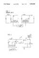
- FIG. 1illustrates a battery charge/discharge configuration known in the prior art.
- the circuit of FIG. 1includes separate circuits for charging and discharging the battery.
- the charge and discharge circuitseach have their own controller.
- the interaction of the charge and discharge circuitsis controlled by steering logic that is coupled to the charge controller and the discharge controller.
- steering logiccan be very complex and also is an area of possible instability due to the interaction between the charge and discharge circuits.
- weightis a primary consideration because of the tremendous launch and payload costs for spacecraft.
- the battery charge/discharge circuit of FIG. 1is particularly a problem since separate circuits are required to perform the charging and discharging functions; thus, the power converters add to the weight of the satellite.
- a further problem with the converters of the prior artis reliability. Since the power converters will be used in satellites, they will not be easily accessible once placed in operation. Thus, separate controlling circuits and complex steering logic are areas were the converters are likely to malfunction. This tends to reduced the reliability of the entire satellite.
- a preferred embodiment of the power system of the present inventioncomprises a battery (12), an inductor (14) switching means (18, 20), an inverter (22), and a controller (16).
- the battery (12)preferably has first and second terminals.
- the inductor (14)has a first and a second end, and the first end of the inductor (14) is coupled to the first terminal of the battery (12).
- the switching means (18, 20)selectively couples the second end of the inductor (14) to a bus (28) or to ground in response to a control signal.
- the switching means (18, 20)is coupled between the second end of the inductor (14), the bus (28) and ground.
- the controller (16)is preferably coupled to receive control signals from a computer (13) on board the satellite, and outputs a signal for controlling the switching means (18, 20).
- the output of the controller (16)is also coupled to the inverter (22), whose output provides another signal for controlling the switching means (18, 20).
- the controller (16)monitors the bus (28) voltage, current flow to the battery (12), and the current flow through the switching means (18, 20).
- the controller (16)also receives control signals from the satellite's computer (13) and automatically regulates the voltage on the bus (28) by adjusting the duty cycle of the signal output by the controller (16).
- the bilateral converter (10)acts either as a buck converter, or as a boost converter to charge or discharge the battery according to the amount of power on the bus (28).
- FIG. 1is a block diagram of a prior art satellite power system
- FIG. 2is a block diagram of a preferred embodiment of the bilateral power converter of the present invention for satellites
- FIG. 3is a schematic diagram of tile preferred embodiment of the bilateral power converter of the present invention.
- FIG. 4is a schematic diagram of a preferred embodiment of an inner control loop which may be incorporated into the bilateral power converter system of the present invention
- FIG. 5is a schematic diagram of a preferred embodiment of an outer control loop which may be incorporated into the bilateral power converter system of the present invention.
- the present inventionis a bilateral power converter 10 for use in satellite power systems.
- a solar array 15is provided to convert radiant energy into electrical energy for use by the satellite.
- a battery 12powers the satellite when the solar array 15 does not generate enough power to satisfy the requirements of the satellite.
- the prior artconventionally uses separate power converters to couple the solar array 15 and the battery 12 together according to the amount of power generated by the solar array 15. Excess power from the solar array 15 is also used to charge the battery 12.
- the present inventionadvantageously combines the separate power converters into a bilateral power converter for significant weight savings and improved reliability.
- the bilateral power converter 10attempts to maintain a power bus 28 of the satellite at a preset voltage by either sinking or sourcing current to the bus 28.
- FIG. 2a simplified block diagram of a preferred embodiment of a satellite power system constructed in accordance with the present invention is shown.
- the present inventionis preferably controlled in part by the satellite's computer 13.
- the bilateral converter 10preferably comprises an inductor 14, a controller 16, a first switch 18, a second switch 20, an inverter 22 and a capacitor 24.
- the converter 10is bilateral in that power can flow both to charge and discharge the battery 12.
- the converter 10effectively either sinks or sources power to the bus 28 in response to signals from the controller 16.
- the battery 12has a first terminal and a second terminal.
- the first terminalis preferably coupled to a first end of the inductor 14.
- the second terminalprovides ground.
- the first switch 18is preferably coupled between the second terminal of the battery 12 and a second end of the inductor 14.
- the capacitor 24also has one end coupled to the second terminal of the battery 12.
- the second switch 20is coupled between the second end of the inductor 14 and the other end of the capacitor 24.
- the second switch 20is in a closed position, the current through inductor 14 is increasing in the direction of the battery 12. Therefore, in accordance with the voltage level of the battery 12 and bus 28, and by varying the duty cycle of tile control signal received by the first and second switches 18, 20, the battery 12 will either be charged or discharged.
- the present inventionadvantageously uses a single control signal to control the closing of the first and second switches 18, 20.
- the control signal output by the controller 16is coupled to activate the first switch 18.
- the same control signalis also coupled through inverter 22 to activate the second switch 20.
- the use of a single signal to control the first and second switches 18, 20advantageously eliminates redundant control logic required by the prior art. Since the first and second switches 18, 20 are activated by control signals that are the inverse of each other, only one of the switches 18, 20 will remain closed at any particular instant. Thus, the present invention also eliminates the need for steering logic as required by the prior art device of FIG. 1.
- the first switch 18couples one end of the inductor 14 to ground.
- the second switch 20is coupled between the same end of inductor 14 and the bus 28.
- the other end of the inductor 14is coupled through a resistor 30 to the battery 12.
- the two ends of the resistor 30are coupled to separate inputs of an operational amplifier 32 to produce a signal indicating whether current is flowing to the battery 12.
- the output of amplifier 32is coupled to an input of amplifier 34.
- the other input of amplifier 34is coupled to receive the I charge signal.
- the I charge signalis a signal produced by the computer 13 of the satellite and indicates the desired charge rate for the battery 12.
- the I charge signalalso allows the computer 13 to control the amount of charge that the battery 12 will receive based on its charge state and other factors such as the battery's age.
- Operational amplifier 34compares the I charge signal to the amount of current sent to the battery 12 as indicated by the output of amplifier 32. The output of amplifier 34 is then coupled to node A (the controller 16) by a diode 36 to control the amount of charging current that is provided to the battery 12.
- a plurality of such bilateral converter circuitsBCDU2, BCDU3
- BCDU2, BCDU3may be coupled together to regulate the power between a solar array 15 a several batteries.
- the cathode of the diode 36is preferably coupled to receive signals from other converters (BCDU2, BCDU3).
- the controller 16preferably comprises a multiplier circuit 44 and a pulsewidth modulator 40 including an operational amplifier 42.
- the pulsewidth modulator 40has a first control input that is coupled to receive the V set signal.
- the V set signalis a threshold voltage provided by the computer 13 to regulate the bus 28 independent of whether the battery 12 is being discharged or charged.
- the pulsewidth modulator 40has a second control input coupled to the bus 28 by a resistor 46.
- the pulsewidth modulator 40includes an operational amplifier 48 that compares the V set signal and the bus 28 voltage to regulate the output of the pulsewidth modulator 40.
- the output of the amplifier 48is preferably coupled by a diode to node A, and thus, provides a feedback loop for amplifier 48.
- the pulsewidth modulator 40also receives input from the multiplier circuit 44.
- the multiplier circuit 44preferably has two inputs.
- the first inputis coupled to receive a proportionality constant signal from the satellite's computer 13.
- the proportionality constant signalis used by the computer 13 to regulate the percentage of the total power that each bilateral converter 10 can deliver or receive.
- the proportionality constantmay be varied such that one BCDU (Battery Charging Discharging Unit) may deliver 50% of the power while two other BCDUs each deliver 25% of the power.
- the other input to the multiplier circuit 44is provided by the output of amplifier 42 that provides a signal indicative of the amount of current passing through the first switch 18, and thus through this particular bilateral converter or BCDU.
- the multiplier circuit 44multiplies the signal output by amplifier 42 by the proportionality constant signal and sends the product to the pulsewidth modulator 40 in order to set the ratio control of current to the battery 12 relative to the other converters.
- the pulsewidth modulator 40is also coupled to receive the output of amplifier 42.
- amplifier 42provides a signal indicative of the amount of current passing through the first switch 18.
- a first input of the amplifier 42is coupled to ground through a resistor 48.
- the first input of amplifier 42is also coupled to the output of amplifier 42 by resistor 52.
- a second input of the amplifier 42is coupled by a resistor 50 to an end of the first switch 18.
- the output of the pulsewidth modulator 40is used to control the closing of the first and second switches 18, 20.
- two outputs of the pulsewidth modulator 40are coupled to diodes 54 and "OR" together to provide a signal with a wider range of duty cycle.
- the outputs of the diodes 54are coupled through an inverter 56 to the control input of the first switch 18.
- outputs of the diodes 54are coupled through a resistor 58, an optical coupling device 60, and inverter 22 to the control input of the second switch 20.
- the first and second switches 18, 20are field effect transistors. Since the first and second switches 18, 20 are controlled by a single control signal and its inverse, the switches 18, 20 must be one of two possible states.
- the first switch 18In the first state, the first switch 18 is open and the second switch 20 is closed, and an electrical path through the second switch 20 allows current to flow from the bus 28 through the inductor 14 to the battery 12, or vice versa.
- the first switch 18In the second state, the first switch 18 is closed and the second switch 20 is open, which disconnects the bus 28 from the inductor 14 and couples one end of the inductor 14 to ground through a resistor.
- the pulsewidth modulator 40advantageously varies the duty cycle of its output signal according to the input signals received.
- the bilateral converteracts 10 as either a boost or a buck converter, and thus, can drive power in both directions. For example, if the power provided by the solar array 15 on bus 28 is adequate to drive the satellite's system loads as well as charge the battery 12, then the error amplifier 48 will be driven into saturation. The battery charging current will be controlled by the programed value by limiting the error amplifier excursion 48 by a current sense amplifier 42.
- the converter 10continuously regulates the bus voltage by adjusting the duty cycle output by the pulsewidth modulator 40 independent of the mode in which the converter 10 is operating.
- the depicted elementsappear once in the converter, the elements of the preferred embodiment of FIG. 4 being attached in one or more embodiments all together at the nodes shown in FIG. 5.
- the outer, voltage control loopcontains a resistor divider network 100, a plenitude of buffers 101 to communicate the signal generated by 100 to all other converters in the system, and an amplifier 48.
- the amplifierhas a first control input that is coupled to receive the Vset signal.
- the Vset signalis a voltage provided by the computer (not shown) to regulate the bus (28) voltage.
- the amplifier 48has a second input coupled to the bus by the resistor divider network 100.
- the amplifierhas feedback 102 to control the frequency characteristics of ths bus control.
- the voltage control loopalso consists of a diode 103 to determine which of the various signals attached to the node Vcontrol will control the duty cycle.
- the loopalso contains a plenitude of control inputs, one for each other converter in the system. Each of these is coupled to the node Vcontrol through a diode, such as 104 in the Figure, with which they are connected in a manner that the highest signal controls the duty cycle.
- the outer, current limiting control loopcontains a resistor 30 to sense total current into or out of the battery.
- the common-mode voltage of this signalis removed by amplifier 32, which also amplifies the signal.
- Amplifier 32has an input from node (B), connected to the nodes (B) represented in FIG. 4, and a second input from the battery.
- the output of amplifier 32is one input to amplifier 34.
- Amplifier 34has a second input, which is a voltage provided by the computer (not shown) to limit the maximum charge current into the battery.
- Amplifier 34also has feedback 105 to control the frequency characteristics of the current control loop, and a diode 36 to couple it to the node Vcontrol, with which it is connected in a manner that the highest signal controls the duty cycle.
- FIG. 5also shows a portion of the inner, high-frequency average current loop.
- the output of the amplifier 32is connected to one input of a multiplier, 44.
- the other input of the multiplieris connected to the Proportionality constant signal.
- the proportionality constant signalis a voltage provided by the computer (not shown) to determine the ratios of currents being provided to or from the battery attached to each converter (the batteries need not be each of the same voltage).
- the output of the multiplier 44is attached to a (possibly active) filter network 106, which shapes the frequency characteristics of the inner control loop signal provided at the node Icontrol to the rest of the inner control loops represented in FIG. 4.
- a first switch 20is connected to the node (A) of FIG. 5. It is also connected to an inductor 14, and to a second switch 18. Switch 18 is connected via a current sensing resistor 107 to ground.
- the inductor 14is also connected to the node (B) of FIG. 5.
- the current sensed in resistor 107is a peak-current. It is added in adder 42 to the total current control voltage Icontrol, produced on FIG. 5. In the preferred embodiment, the peak current would be about 5% of the amplitude of the total current. The addition of the peak current to the total current ensures that each occurrence of the FIG. 4 within the converter will take an equal share of the total current of the converter.
- the output of the adder 42is connected to one input of the amplifier 108.
- a second input to amplifier 108is connected to the node Vcontrol, which is generated on FIG. 5, and is the outer control loop signal controlling the inner loop.
- the amplifier 108also has a feedback 109 which controls the frequency characteristics of the inner control loop.
- the output of the amplifier 108is one input to the pulse-width modulator 40, which converts its input signals into a duty cycle.
- the other input to the pwm 40is for the system clock, through a delay 110.
- the delayis different for each example of FIG. 4 included within the converter, the delay serving to stagger the units to reduce input and output ripples of the converter.
- the delayed system clockacts to initiate the duty cycle of the pwm 40.
- the output of the pulse-width modulator 40is a duty cycle modulated signal used to control the two switches, 18 and 20.
- Switch 18is controlled directly by the pwm 40, whereas switch 20 is controlled by the inverted signal from the pwm, the inversion being accomplished by inverter 22.
- Inverter 22also acts to convert the drive signal to the appropriate voltage level for switch 20.
Landscapes
- Engineering & Computer Science (AREA)
- Power Engineering (AREA)
- Remote Sensing (AREA)
- Aviation & Aerospace Engineering (AREA)
- Physics & Mathematics (AREA)
- Electromagnetism (AREA)
- General Physics & Mathematics (AREA)
- Radar, Positioning & Navigation (AREA)
- Automation & Control Theory (AREA)
- Dc-Dc Converters (AREA)
Abstract
Description
Claims (14)
Priority Applications (2)
| Application Number | Priority Date | Filing Date | Title |
|---|---|---|---|
| US08/192,186US5359280A (en) | 1992-01-10 | 1994-02-04 | Bilateral power converter for a satellite power system |
| US08/278,939US5477132A (en) | 1992-01-10 | 1994-07-22 | Multi-sectioned power converter having current-sharing controller |
Applications Claiming Priority (2)
| Application Number | Priority Date | Filing Date | Title |
|---|---|---|---|
| US81884292A | 1992-01-10 | 1992-01-10 | |
| US08/192,186US5359280A (en) | 1992-01-10 | 1994-02-04 | Bilateral power converter for a satellite power system |
Related Parent Applications (1)
| Application Number | Title | Priority Date | Filing Date |
|---|---|---|---|
| US81884292AContinuation | 1992-01-10 | 1992-01-10 |
Related Child Applications (1)
| Application Number | Title | Priority Date | Filing Date |
|---|---|---|---|
| US08/278,939Continuation-In-PartUS5477132A (en) | 1992-01-10 | 1994-07-22 | Multi-sectioned power converter having current-sharing controller |
Publications (1)
| Publication Number | Publication Date |
|---|---|
| US5359280Atrue US5359280A (en) | 1994-10-25 |
Family
ID=25226568
Family Applications (1)
| Application Number | Title | Priority Date | Filing Date |
|---|---|---|---|
| US08/192,186Expired - Fee RelatedUS5359280A (en) | 1992-01-10 | 1994-02-04 | Bilateral power converter for a satellite power system |
Country Status (1)
| Country | Link |
|---|---|
| US (1) | US5359280A (en) |
Cited By (54)
| Publication number | Priority date | Publication date | Assignee | Title |
|---|---|---|---|---|
| US5477132A (en)* | 1992-01-10 | 1995-12-19 | Space Systems/Loral, Inc. | Multi-sectioned power converter having current-sharing controller |
| US5479089A (en)* | 1994-12-21 | 1995-12-26 | Hughes Aircraft Company | Power converter apparatus having instantaneous commutation switching system |
| US5530335A (en)* | 1993-05-11 | 1996-06-25 | Trw Inc. | Battery regulated bus spacecraft power control system |
| EP0712214A3 (en)* | 1994-11-08 | 1996-07-24 | Loral Space Systems Inc | Power control system of a satellite communication device |
| US5592074A (en)* | 1992-06-26 | 1997-01-07 | Canon Kabushiki Kaisha | Battery power supply system |
| US5594324A (en)* | 1995-03-31 | 1997-01-14 | Space Systems/Loral, Inc. | Stabilized power converter having quantized duty cycle |
| US5602464A (en)* | 1995-07-24 | 1997-02-11 | Martin Marietta Corp. | Bidirectional power converter modules, and power system using paralleled modules |
| US5637978A (en)* | 1995-11-06 | 1997-06-10 | Kendrick Products Corporation | Battery booster |
| WO1998015997A1 (en)* | 1996-10-10 | 1998-04-16 | Chartec Laboratories A/S | A digitally controlled switch mode power supply for charging rechargeable batteries |
| US5751140A (en)* | 1997-03-25 | 1998-05-12 | Space Systems/Loreal, Inc. | Voltage converter with battery discharge protection |
| US5814979A (en)* | 1995-06-01 | 1998-09-29 | Maxim Integrated Products, Inc. | Low drop out switching regulator |
| FR2762721A1 (en)* | 1997-04-29 | 1998-10-30 | Sagem | METHOD FOR CHARGING A BATTERY AND BATTERY CHARGER FOR IMPLEMENTING THE METHOD |
| US5844399A (en)* | 1996-07-26 | 1998-12-01 | The University Of Toledo | Battery charger control system |
| US5895982A (en)* | 1996-05-02 | 1999-04-20 | Hughes Electronics Corporation | Fully regulated power bus using multiple source bus regulators |
| US5960075A (en)* | 1995-02-16 | 1999-09-28 | Northern Telecom Limited | Switchmode power converters for telephone subscriber line interface circuits |
| US6002603A (en)* | 1999-02-25 | 1999-12-14 | Elliott Energy Systems, Inc. | Balanced boost/buck DC to DC converter |
| US6031743A (en)* | 1998-10-28 | 2000-02-29 | International Business Machines Corporation | Fault isolation in a redundant power converter |
| US6046570A (en)* | 1997-03-07 | 2000-04-04 | Interplex Energy Ltd. | Waveform generator and control circuit |
| EP1030431A1 (en)* | 1999-02-19 | 2000-08-23 | Sagem Sa | Device for charge transfer between two batteries |
| WO2000067366A1 (en)* | 1999-05-04 | 2000-11-09 | Koninklijke Philips Electronics N.V. | Dc-dc converter |
| WO2000074200A1 (en)* | 1999-05-27 | 2000-12-07 | Alan Henry Weinberg | Battery charging and discharging system |
| US6268666B1 (en)* | 1999-02-25 | 2001-07-31 | Southwest Research Institute | Bi-directional power conversion apparatus for combination of energy sources |
| US6275958B1 (en) | 1998-10-28 | 2001-08-14 | International Business Machines Corporation | Fault detection in a redundant power converter |
| US6348781B1 (en)* | 2000-12-11 | 2002-02-19 | Motorola, Inc. | Buck or boost power converter |
| US6369555B2 (en)* | 2000-05-15 | 2002-04-09 | Texas Instruments Incorporated | Integrated low ripple, high frequency hysteretic controller for DC-DC converters |
| US6380712B2 (en)* | 2000-04-10 | 2002-04-30 | Kenneth C. Murphy | Battery booster with preconditioning and temperature compensation |
| FR2824203A1 (en)* | 2001-04-27 | 2002-10-31 | Agence Spatiale Europeenne | POWER SUPPLY CONVERTER |
| US20030090245A1 (en)* | 2001-11-05 | 2003-05-15 | Krishna Shenai | Synchronous switched boost and buck converter |
| US20030197494A1 (en)* | 2001-06-07 | 2003-10-23 | Hitachi, Ltd. | DC-DC converter and a method of controlling thereof |
| US20030230334A1 (en)* | 2002-06-13 | 2003-12-18 | Koninklijke Philips Electronics N.V. | Autonomous solid state lighting system |
| US6765370B2 (en)* | 2002-05-17 | 2004-07-20 | Kyocera Wireless Corp. | System and method for bi-directional power conversion in a portable device |
| US20040207370A1 (en)* | 2003-04-17 | 2004-10-21 | Toyoda Koki Kabushiki Kaisha | Booster circuit and method for controlling the same |
| US20040217745A1 (en)* | 2003-04-30 | 2004-11-04 | Winbond Electronics Corp. | Power regulator |
| US20050035747A1 (en)* | 2003-08-11 | 2005-02-17 | Semiconductor Components Industries, Llc | Method of forming a high efficiency power controller |
| US20050073866A1 (en)* | 2003-10-07 | 2005-04-07 | John Cummings | Boost converters, power supply apparatuses, electrical energy boost methods and electrical energy supply methods |
| US6987378B1 (en)* | 2004-12-02 | 2006-01-17 | Semiconductor Components Industries, L.L.C. | Over-voltage protection circuit and method therefor |
| US20060055351A1 (en)* | 2004-09-01 | 2006-03-16 | FAVESS Co, Ltd. | Electric power steering apparatus and booster |
| US7098634B1 (en)* | 2003-02-21 | 2006-08-29 | Lovoltech, Inc. | Buck-boost circuit with normally off JFET |
| US20060238174A1 (en)* | 2005-04-25 | 2006-10-26 | Catalyst Semiconductor, Inc. | LED current bias control using a step down regulator |
| US20070235071A1 (en)* | 2006-04-06 | 2007-10-11 | Work Jason N | Adaptive solar powered system |
| EP1990887A1 (en)* | 2007-05-07 | 2008-11-12 | STMicroelectronics S.r.l. | A power management unit for battery-operated devices |
| CN101917043A (en)* | 2010-08-19 | 2010-12-15 | 中国电子科技集团公司第十八研究所 | Lithium-ion battery charge and discharge control circuit |
| US20110005567A1 (en)* | 2007-04-06 | 2011-01-13 | Sunovia Energy Technologies Inc. | Modular solar panel system |
| JP2012228169A (en)* | 2011-04-15 | 2012-11-15 | Boeing Co:The | Bi-directional converter voltage controlled current source for voltage regulation |
| US8441231B2 (en) | 2011-05-27 | 2013-05-14 | Eta Semiconductor Inc. | Bidirectional hysteretic power converter |
| US20130162234A1 (en)* | 2011-12-27 | 2013-06-27 | Richtek Technology Corporation | Buck regulation of a boost regulator |
| US8498172B1 (en) | 2010-08-31 | 2013-07-30 | Western Digital Technologies, Inc. | Data storage device evaluating frequency range of supply voltage to detect power failure |
| US20130307490A1 (en)* | 2012-04-24 | 2013-11-21 | Semiconductor Components Industries, Llc | Charge control circuit, charge circuit, and mobile device |
| US20140049235A1 (en)* | 2012-08-14 | 2014-02-20 | Chengdu Monolithic Power Systems Co., Ltd. | Switching regulator and the method thereof |
| US20140211529A1 (en)* | 2013-01-28 | 2014-07-31 | General Electric Company | Methods and systems for operating a bi-directional micro inverter |
| US20150008867A1 (en)* | 2013-07-03 | 2015-01-08 | At&T Intellectual Property I, L.P. | Charge pump battery charging |
| EP2523329A3 (en)* | 2011-01-30 | 2017-06-07 | The Boeing Company | Voltage controlled current source for voltage regulation |
| CN108139447A (en)* | 2015-10-13 | 2018-06-08 | 罗伯特·博世有限公司 | Vehicle, device and method for determining the voltage of a battery in a string of a plurality of series-connected batteries of an electrochemical energy store |
| CN109904853A (en)* | 2019-04-19 | 2019-06-18 | 四川长虹电源有限责任公司 | DC power system and electrical equipment |
Citations (8)
| Publication number | Priority date | Publication date | Assignee | Title |
|---|---|---|---|---|
| GB2088159A (en)* | 1980-11-20 | 1982-06-03 | Harmer & Simmons Ltd | Battery Charging Apparatus |
| US4347474A (en)* | 1980-09-18 | 1982-08-31 | The United States Of America As Represented By The Secretary Of The Navy | Solid state regulated power transformer with waveform conditioning capability |
| US4549254A (en)* | 1983-02-03 | 1985-10-22 | Chrysler Corporation | Buck-boost regulated D.C. to D.C. power supply |
| US4672303A (en)* | 1986-08-28 | 1987-06-09 | International Business Machines Corporation | Inductor current control circuit |
| US4729088A (en)* | 1987-05-11 | 1988-03-01 | Advance Transformer Company | Regulated high frequency power supply |
| US4736151A (en)* | 1986-12-23 | 1988-04-05 | Sundstrand Corporation | Bi-directional buck/boost DC/DC converter |
| US4801859A (en)* | 1986-12-23 | 1989-01-31 | Sundstrand Corporation | Boost/buck DC/DC converter |
| US4947311A (en)* | 1989-11-16 | 1990-08-07 | General Electric Company | Electrical power conversion circuit |
- 1994
- 1994-02-04USUS08/192,186patent/US5359280A/ennot_activeExpired - Fee Related
Patent Citations (8)
| Publication number | Priority date | Publication date | Assignee | Title |
|---|---|---|---|---|
| US4347474A (en)* | 1980-09-18 | 1982-08-31 | The United States Of America As Represented By The Secretary Of The Navy | Solid state regulated power transformer with waveform conditioning capability |
| GB2088159A (en)* | 1980-11-20 | 1982-06-03 | Harmer & Simmons Ltd | Battery Charging Apparatus |
| US4549254A (en)* | 1983-02-03 | 1985-10-22 | Chrysler Corporation | Buck-boost regulated D.C. to D.C. power supply |
| US4672303A (en)* | 1986-08-28 | 1987-06-09 | International Business Machines Corporation | Inductor current control circuit |
| US4736151A (en)* | 1986-12-23 | 1988-04-05 | Sundstrand Corporation | Bi-directional buck/boost DC/DC converter |
| US4801859A (en)* | 1986-12-23 | 1989-01-31 | Sundstrand Corporation | Boost/buck DC/DC converter |
| US4729088A (en)* | 1987-05-11 | 1988-03-01 | Advance Transformer Company | Regulated high frequency power supply |
| US4947311A (en)* | 1989-11-16 | 1990-08-07 | General Electric Company | Electrical power conversion circuit |
Cited By (79)
| Publication number | Priority date | Publication date | Assignee | Title |
|---|---|---|---|---|
| US5477132A (en)* | 1992-01-10 | 1995-12-19 | Space Systems/Loral, Inc. | Multi-sectioned power converter having current-sharing controller |
| US5592074A (en)* | 1992-06-26 | 1997-01-07 | Canon Kabushiki Kaisha | Battery power supply system |
| US5530335A (en)* | 1993-05-11 | 1996-06-25 | Trw Inc. | Battery regulated bus spacecraft power control system |
| US5826170A (en)* | 1994-11-08 | 1998-10-20 | Space Systems/Loral, Inc. | Satellite communication power management system |
| EP0712214A3 (en)* | 1994-11-08 | 1996-07-24 | Loral Space Systems Inc | Power control system of a satellite communication device |
| US5787336A (en)* | 1994-11-08 | 1998-07-28 | Space Systems/Loral, Inc. | Satellite communication power management system |
| CN1084980C (en)* | 1994-11-08 | 2002-05-15 | 太空系统/罗拉尔有限公司 | Stellite communication power management system |
| US5479089A (en)* | 1994-12-21 | 1995-12-26 | Hughes Aircraft Company | Power converter apparatus having instantaneous commutation switching system |
| US5960075A (en)* | 1995-02-16 | 1999-09-28 | Northern Telecom Limited | Switchmode power converters for telephone subscriber line interface circuits |
| US5594324A (en)* | 1995-03-31 | 1997-01-14 | Space Systems/Loral, Inc. | Stabilized power converter having quantized duty cycle |
| US5955872A (en)* | 1995-06-01 | 1999-09-21 | Maxim Integrated Products, Inc. | Low drop-out switching regulators |
| US5814979A (en)* | 1995-06-01 | 1998-09-29 | Maxim Integrated Products, Inc. | Low drop out switching regulator |
| US5602464A (en)* | 1995-07-24 | 1997-02-11 | Martin Marietta Corp. | Bidirectional power converter modules, and power system using paralleled modules |
| US5637978A (en)* | 1995-11-06 | 1997-06-10 | Kendrick Products Corporation | Battery booster |
| US5895982A (en)* | 1996-05-02 | 1999-04-20 | Hughes Electronics Corporation | Fully regulated power bus using multiple source bus regulators |
| US5844399A (en)* | 1996-07-26 | 1998-12-01 | The University Of Toledo | Battery charger control system |
| WO1998015997A1 (en)* | 1996-10-10 | 1998-04-16 | Chartec Laboratories A/S | A digitally controlled switch mode power supply for charging rechargeable batteries |
| US6031359A (en)* | 1996-10-10 | 2000-02-29 | Chartec Laboratories A/S | Digitally controlled switch mode power supply for charging rechargeable batteries |
| US6046570A (en)* | 1997-03-07 | 2000-04-04 | Interplex Energy Ltd. | Waveform generator and control circuit |
| US5751140A (en)* | 1997-03-25 | 1998-05-12 | Space Systems/Loreal, Inc. | Voltage converter with battery discharge protection |
| US6025697A (en)* | 1997-04-29 | 2000-02-15 | Sagem S.A. | Process for charging a battery and battery charger to achieve the process |
| FR2762721A1 (en)* | 1997-04-29 | 1998-10-30 | Sagem | METHOD FOR CHARGING A BATTERY AND BATTERY CHARGER FOR IMPLEMENTING THE METHOD |
| US6031743A (en)* | 1998-10-28 | 2000-02-29 | International Business Machines Corporation | Fault isolation in a redundant power converter |
| US6275958B1 (en) | 1998-10-28 | 2001-08-14 | International Business Machines Corporation | Fault detection in a redundant power converter |
| EP1030431A1 (en)* | 1999-02-19 | 2000-08-23 | Sagem Sa | Device for charge transfer between two batteries |
| FR2790147A1 (en)* | 1999-02-19 | 2000-08-25 | Sagem | CHARGE CURRENT TRANSFER DEVICE BETWEEN TWO BATTERIES |
| US6002603A (en)* | 1999-02-25 | 1999-12-14 | Elliott Energy Systems, Inc. | Balanced boost/buck DC to DC converter |
| US6268666B1 (en)* | 1999-02-25 | 2001-07-31 | Southwest Research Institute | Bi-directional power conversion apparatus for combination of energy sources |
| US6191567B1 (en) | 1999-05-04 | 2001-02-20 | U.S. Philips Corporation | DC-DC converter, with duty cycle comparison for a dual mode back boost converter |
| WO2000067366A1 (en)* | 1999-05-04 | 2000-11-09 | Koninklijke Philips Electronics N.V. | Dc-dc converter |
| WO2000074200A1 (en)* | 1999-05-27 | 2000-12-07 | Alan Henry Weinberg | Battery charging and discharging system |
| US6380712B2 (en)* | 2000-04-10 | 2002-04-30 | Kenneth C. Murphy | Battery booster with preconditioning and temperature compensation |
| US6369555B2 (en)* | 2000-05-15 | 2002-04-09 | Texas Instruments Incorporated | Integrated low ripple, high frequency hysteretic controller for DC-DC converters |
| US6348781B1 (en)* | 2000-12-11 | 2002-02-19 | Motorola, Inc. | Buck or boost power converter |
| FR2824203A1 (en)* | 2001-04-27 | 2002-10-31 | Agence Spatiale Europeenne | POWER SUPPLY CONVERTER |
| US6617831B2 (en) | 2001-04-27 | 2003-09-09 | Agence Spatiale Europeenne | Electrical power supply converter |
| US20030197494A1 (en)* | 2001-06-07 | 2003-10-23 | Hitachi, Ltd. | DC-DC converter and a method of controlling thereof |
| WO2003041251A1 (en)* | 2001-11-05 | 2003-05-15 | Shakti Systems, Inc. | Synchronous switched boost and buck converter |
| US20030090245A1 (en)* | 2001-11-05 | 2003-05-15 | Krishna Shenai | Synchronous switched boost and buck converter |
| WO2003041250A1 (en)* | 2001-11-05 | 2003-05-15 | Shakti Systems, Inc. | Dc-dc converter with current control |
| US6765370B2 (en)* | 2002-05-17 | 2004-07-20 | Kyocera Wireless Corp. | System and method for bi-directional power conversion in a portable device |
| JP2005530325A (en)* | 2002-06-13 | 2005-10-06 | コーニンクレッカ フィリップス エレクトロニクス エヌ ヴィ | Stand-alone solid state lighting system |
| US20030230334A1 (en)* | 2002-06-13 | 2003-12-18 | Koninklijke Philips Electronics N.V. | Autonomous solid state lighting system |
| WO2003107722A3 (en)* | 2002-06-13 | 2004-07-22 | Koninkl Philips Electronics Nv | Autonomous solid state lighting system |
| US7098634B1 (en)* | 2003-02-21 | 2006-08-29 | Lovoltech, Inc. | Buck-boost circuit with normally off JFET |
| US20040207370A1 (en)* | 2003-04-17 | 2004-10-21 | Toyoda Koki Kabushiki Kaisha | Booster circuit and method for controlling the same |
| US7026796B2 (en)* | 2003-04-17 | 2006-04-11 | Toyoda Koki Kabushiki Kaisha | Booster circuit and method for controlling the same |
| US20040217745A1 (en)* | 2003-04-30 | 2004-11-04 | Winbond Electronics Corp. | Power regulator |
| US20050035747A1 (en)* | 2003-08-11 | 2005-02-17 | Semiconductor Components Industries, Llc | Method of forming a high efficiency power controller |
| US6936997B2 (en)* | 2003-08-11 | 2005-08-30 | Semiconductor Components Industries, Llc | Method of forming a high efficiency power controller |
| CN100489723C (en)* | 2003-08-11 | 2009-05-20 | 半导体元件工业有限责任公司 | Method for forming efficient power controller |
| US20050073866A1 (en)* | 2003-10-07 | 2005-04-07 | John Cummings | Boost converters, power supply apparatuses, electrical energy boost methods and electrical energy supply methods |
| US20060055351A1 (en)* | 2004-09-01 | 2006-03-16 | FAVESS Co, Ltd. | Electric power steering apparatus and booster |
| US7129663B2 (en)* | 2004-09-01 | 2006-10-31 | Favess Co., Ltd. | Electric power steering apparatus and booster |
| US6987378B1 (en)* | 2004-12-02 | 2006-01-17 | Semiconductor Components Industries, L.L.C. | Over-voltage protection circuit and method therefor |
| US7323828B2 (en)* | 2005-04-25 | 2008-01-29 | Catalyst Semiconductor, Inc. | LED current bias control using a step down regulator |
| WO2006116576A3 (en)* | 2005-04-25 | 2007-05-18 | Catalyst Semiconductor Inc | Led current bias control using a step down regulator |
| US20060238174A1 (en)* | 2005-04-25 | 2006-10-26 | Catalyst Semiconductor, Inc. | LED current bias control using a step down regulator |
| US20070235071A1 (en)* | 2006-04-06 | 2007-10-11 | Work Jason N | Adaptive solar powered system |
| US8779625B2 (en) | 2006-04-06 | 2014-07-15 | Carmanah Technologies Corp. | Adaptive solar powered system |
| US8563845B2 (en) | 2006-04-06 | 2013-10-22 | Carmanah Technologies Corp. | Adaptive solar powered system |
| US20110005567A1 (en)* | 2007-04-06 | 2011-01-13 | Sunovia Energy Technologies Inc. | Modular solar panel system |
| EP1990887A1 (en)* | 2007-05-07 | 2008-11-12 | STMicroelectronics S.r.l. | A power management unit for battery-operated devices |
| CN101917043A (en)* | 2010-08-19 | 2010-12-15 | 中国电子科技集团公司第十八研究所 | Lithium-ion battery charge and discharge control circuit |
| CN101917043B (en)* | 2010-08-19 | 2013-01-30 | 中国电子科技集团公司第十八研究所 | Lithium-ion battery charge and discharge control circuit |
| US8498172B1 (en) | 2010-08-31 | 2013-07-30 | Western Digital Technologies, Inc. | Data storage device evaluating frequency range of supply voltage to detect power failure |
| EP2523329A3 (en)* | 2011-01-30 | 2017-06-07 | The Boeing Company | Voltage controlled current source for voltage regulation |
| US9531190B2 (en) | 2011-04-15 | 2016-12-27 | The Boeing Company | Bi-directional converter voltage controlled current source for voltage regulation |
| JP2012228169A (en)* | 2011-04-15 | 2012-11-15 | Boeing Co:The | Bi-directional converter voltage controlled current source for voltage regulation |
| US8441231B2 (en) | 2011-05-27 | 2013-05-14 | Eta Semiconductor Inc. | Bidirectional hysteretic power converter |
| US20130162234A1 (en)* | 2011-12-27 | 2013-06-27 | Richtek Technology Corporation | Buck regulation of a boost regulator |
| US20130307490A1 (en)* | 2012-04-24 | 2013-11-21 | Semiconductor Components Industries, Llc | Charge control circuit, charge circuit, and mobile device |
| US9553461B2 (en)* | 2012-04-24 | 2017-01-24 | Semiconductor Components Industries, Llc | Charge control circuit, charge circuit, and mobile device |
| US20140049235A1 (en)* | 2012-08-14 | 2014-02-20 | Chengdu Monolithic Power Systems Co., Ltd. | Switching regulator and the method thereof |
| US8941367B2 (en)* | 2012-08-14 | 2015-01-27 | Chengdu Monolithic Power Systems Co., Ltd. | Switching regulator and the method of generating a peak current signal for the switching regulator |
| US20140211529A1 (en)* | 2013-01-28 | 2014-07-31 | General Electric Company | Methods and systems for operating a bi-directional micro inverter |
| US20150008867A1 (en)* | 2013-07-03 | 2015-01-08 | At&T Intellectual Property I, L.P. | Charge pump battery charging |
| CN108139447A (en)* | 2015-10-13 | 2018-06-08 | 罗伯特·博世有限公司 | Vehicle, device and method for determining the voltage of a battery in a string of a plurality of series-connected batteries of an electrochemical energy store |
| CN109904853A (en)* | 2019-04-19 | 2019-06-18 | 四川长虹电源有限责任公司 | DC power system and electrical equipment |
Similar Documents
| Publication | Publication Date | Title |
|---|---|---|
| US5359280A (en) | Bilateral power converter for a satellite power system | |
| US5477132A (en) | Multi-sectioned power converter having current-sharing controller | |
| US7759918B2 (en) | Method for inhibiting thermal run-away | |
| US6424207B1 (en) | PWM active filter for DC power systems | |
| US6087816A (en) | Step-up/step-down switching regulators and pulse width modulation control therefor | |
| US5442317A (en) | Switching regulator and amplifier system | |
| US6437547B2 (en) | Board mountable power supply module with multi-function control pin | |
| US5164890A (en) | Current share scheme for parallel operation of power conditioners | |
| CN102804096B (en) | Boost and Buck Conversion Based Solar Array Regulator and Solar Cell Power System Incorporating the Regulator | |
| US6850045B2 (en) | Multi-phase and multi-module power system with a current share bus | |
| US7276886B2 (en) | Dual buck-boost converter with single inductor | |
| KR101280186B1 (en) | Switched mode power converter | |
| US9093901B2 (en) | Switching converter and method for controlling a switching converter | |
| US4709323A (en) | Buck-boost parallel resonant converter with inductive energy recovery circuit | |
| EP0993104A2 (en) | Capacitive-summing switch-mode power conversion control and method | |
| US5253157A (en) | Half-bridge inverter with capacitive voltage equalizer | |
| EP0762623A3 (en) | Power conversion apparatus | |
| US5397976A (en) | Control system for voltage controlled bilateral current source | |
| GB2480614A (en) | Selectable path switched mode power supply | |
| US5691627A (en) | Push-pull full shunt switching bus voltage limiter with current sense capability | |
| US20020109415A1 (en) | Switched capacitor array circuits having universal rest state and method | |
| US20120286579A1 (en) | Electrical power conditioning unit and system | |
| US5430405A (en) | Control circuit for converters operating in the discontinuous mode | |
| US6191569B1 (en) | Circuit and method for generating estimated feedback for the controller of a slave power module in a master/slave paralleling scheme | |
| Middlebrook et al. | A new battery charger/discharger converter |
Legal Events
| Date | Code | Title | Description |
|---|---|---|---|
| FEPP | Fee payment procedure | Free format text:PAYOR NUMBER ASSIGNED (ORIGINAL EVENT CODE: ASPN); ENTITY STATUS OF PATENT OWNER: LARGE ENTITY | |
| FPAY | Fee payment | Year of fee payment:4 | |
| FPAY | Fee payment | Year of fee payment:8 | |
| REMI | Maintenance fee reminder mailed | ||
| AS | Assignment | Owner name:BANK OF AMERICA, N.A., AS COLLATERAL AGENT, NORTH Free format text:NOTICE OF GRANT OF SECURITY INTEREST;ASSIGNOR:SPACE SYSTEMS/LORAL INC.;REEL/FRAME:012946/0061 Effective date:20011221 | |
| AS | Assignment | Owner name:SPACE SYSTEMS/LORAL, INC., CALIFORNIA Free format text:RELEASE OF SECURITY INTEREST;ASSIGNOR:BANK OF AMERICA, N.A.;REEL/FRAME:016153/0507 Effective date:20040802 | |
| REMI | Maintenance fee reminder mailed | ||
| LAPS | Lapse for failure to pay maintenance fees | ||
| STCH | Information on status: patent discontinuation | Free format text:PATENT EXPIRED DUE TO NONPAYMENT OF MAINTENANCE FEES UNDER 37 CFR 1.362 | |
| FP | Lapsed due to failure to pay maintenance fee | Effective date:20061025 | |
| AS | Assignment | Owner name:ROYAL BANK OF CANADA, AS THE COLLATERAL AGENT, CANADA Free format text:SECURITY INTEREST;ASSIGNORS:DIGITALGLOBE, INC.;MACDONALD, DETTWILER AND ASSOCIATES LTD.;MACDONALD, DETTWILER AND ASSOCIATES CORPORATION;AND OTHERS;REEL/FRAME:044167/0396 Effective date:20171005 Owner name:ROYAL BANK OF CANADA, AS THE COLLATERAL AGENT, CAN Free format text:SECURITY INTEREST;ASSIGNORS:DIGITALGLOBE, INC.;MACDONALD, DETTWILER AND ASSOCIATES LTD.;MACDONALD, DETTWILER AND ASSOCIATES CORPORATION;AND OTHERS;REEL/FRAME:044167/0396 Effective date:20171005 | |
| AS | Assignment | Owner name:MAXAR SPACE LLC, CALIFORNIA Free format text:TERMINATION AND RELEASE OF SECURITY INTEREST IN PATENTS AND TRADEMARKS - RELEASE OF REEL/FRAME 044167/0396;ASSIGNOR:ROYAL BANK OF CANADA, AS AGENT;REEL/FRAME:063543/0001 Effective date:20230503 Owner name:MAXAR INTELLIGENCE INC., COLORADO Free format text:TERMINATION AND RELEASE OF SECURITY INTEREST IN PATENTS AND TRADEMARKS - RELEASE OF REEL/FRAME 044167/0396;ASSIGNOR:ROYAL BANK OF CANADA, AS AGENT;REEL/FRAME:063543/0001 Effective date:20230503 |