US5356836A - Aluminum plug process - Google Patents
Aluminum plug processDownload PDFInfo
- Publication number
- US5356836A US5356836AUS08/108,224US10822493AUS5356836AUS 5356836 AUS5356836 AUS 5356836AUS 10822493 AUS10822493 AUS 10822493AUS 5356836 AUS5356836 AUS 5356836A
- Authority
- US
- United States
- Prior art keywords
- layer
- angstroms
- sputtering
- cold
- contact opening
- Prior art date
- Legal status (The legal status is an assumption and is not a legal conclusion. Google has not performed a legal analysis and makes no representation as to the accuracy of the status listed.)
- Expired - Lifetime
Links
- 238000000034methodMethods0.000titleclaimsabstractdescription46
- 229910052782aluminiumInorganic materials0.000titleclaimsdescription41
- XAGFODPZIPBFFR-UHFFFAOYSA-NaluminiumChemical compound[Al]XAGFODPZIPBFFR-UHFFFAOYSA-N0.000titleclaimsdescription41
- 229910052751metalInorganic materials0.000claimsabstractdescription47
- 239000002184metalSubstances0.000claimsabstractdescription47
- 238000004544sputter depositionMethods0.000claimsabstractdescription43
- 230000004888barrier functionEffects0.000claimsabstractdescription32
- 238000001465metallisationMethods0.000claimsabstractdescription31
- 239000000758substrateSubstances0.000claimsabstractdescription23
- 239000004065semiconductorSubstances0.000claimsabstractdescription15
- 238000000151depositionMethods0.000claimsdescription30
- 230000008021depositionEffects0.000claimsdescription27
- RTAQQCXQSZGOHL-UHFFFAOYSA-NTitaniumChemical compound[Ti]RTAQQCXQSZGOHL-UHFFFAOYSA-N0.000claimsdescription19
- 229910052719titaniumInorganic materials0.000claimsdescription19
- 239000010936titaniumSubstances0.000claimsdescription19
- 239000011800void materialSubstances0.000claimsdescription13
- 230000015572biosynthetic processEffects0.000claimsdescription10
- NRTOMJZYCJJWKI-UHFFFAOYSA-NTitanium nitrideChemical compound[Ti]#NNRTOMJZYCJJWKI-UHFFFAOYSA-N0.000claimsdescription7
- 229910045601alloyInorganic materials0.000claimsdescription7
- 239000000956alloySubstances0.000claimsdescription7
- VYPSYNLAJGMNEJ-UHFFFAOYSA-NSilicium dioxideChemical compoundO=[Si]=OVYPSYNLAJGMNEJ-UHFFFAOYSA-N0.000claims2
- 235000012239silicon dioxideNutrition0.000claims1
- 239000000377silicon dioxideSubstances0.000claims1
- XKRFYHLGVUSROY-UHFFFAOYSA-NArgonChemical compound[Ar]XKRFYHLGVUSROY-UHFFFAOYSA-N0.000description8
- 229910052710siliconInorganic materials0.000description7
- 229910000838Al alloyInorganic materials0.000description6
- UQZIWOQVLUASCR-UHFFFAOYSA-Nalumane;titaniumChemical compound[AlH3].[Ti]UQZIWOQVLUASCR-UHFFFAOYSA-N0.000description5
- XUIMIQQOPSSXEZ-UHFFFAOYSA-NSiliconChemical compound[Si]XUIMIQQOPSSXEZ-UHFFFAOYSA-N0.000description4
- 229910052786argonInorganic materials0.000description4
- 239000007789gasSubstances0.000description4
- 239000010703siliconSubstances0.000description4
- 229910052802copperInorganic materials0.000description3
- 238000004519manufacturing processMethods0.000description3
- 238000001505atmospheric-pressure chemical vapour depositionMethods0.000description2
- 239000005380borophosphosilicate glassSubstances0.000description2
- 230000001419dependent effectEffects0.000description2
- 238000004518low pressure chemical vapour depositionMethods0.000description2
- 238000000623plasma-assisted chemical vapour depositionMethods0.000description2
- -1AL 1% Si 0.5% CuChemical compound0.000description1
- BOTDANWDWHJENH-UHFFFAOYSA-NTetraethyl orthosilicateChemical compoundCCO[Si](OCC)(OCC)OCCBOTDANWDWHJENH-UHFFFAOYSA-N0.000description1
- 229910001069Ti alloyInorganic materials0.000description1
- 238000005137deposition processMethods0.000description1
- 238000005530etchingMethods0.000description1
- 238000010438heat treatmentMethods0.000description1
- 238000001459lithographyMethods0.000description1
- 239000000463materialSubstances0.000description1
- 229910021421monocrystalline siliconInorganic materials0.000description1
- 230000024121nodulationEffects0.000description1
- MAKDTFFYCIMFQP-UHFFFAOYSA-Ntitanium tungstenChemical compound[Ti].[W]MAKDTFFYCIMFQP-UHFFFAOYSA-N0.000description1
- 238000009736wettingMethods0.000description1
Images


Classifications
- H—ELECTRICITY
- H01—ELECTRIC ELEMENTS
- H01L—SEMICONDUCTOR DEVICES NOT COVERED BY CLASS H10
- H01L21/00—Processes or apparatus adapted for the manufacture or treatment of semiconductor or solid state devices or of parts thereof
- H01L21/70—Manufacture or treatment of devices consisting of a plurality of solid state components formed in or on a common substrate or of parts thereof; Manufacture of integrated circuit devices or of parts thereof
- H01L21/71—Manufacture of specific parts of devices defined in group H01L21/70
- H01L21/768—Applying interconnections to be used for carrying current between separate components within a device comprising conductors and dielectrics
- H01L21/76838—Applying interconnections to be used for carrying current between separate components within a device comprising conductors and dielectrics characterised by the formation and the after-treatment of the conductors
- H01L21/76841—Barrier, adhesion or liner layers
- H01L21/76853—Barrier, adhesion or liner layers characterized by particular after-treatment steps
- H01L21/76855—After-treatment introducing at least one additional element into the layer
- H01L21/76858—After-treatment introducing at least one additional element into the layer by diffusing alloying elements
- H—ELECTRICITY
- H01—ELECTRIC ELEMENTS
- H01L—SEMICONDUCTOR DEVICES NOT COVERED BY CLASS H10
- H01L21/00—Processes or apparatus adapted for the manufacture or treatment of semiconductor or solid state devices or of parts thereof
- H01L21/02—Manufacture or treatment of semiconductor devices or of parts thereof
- H01L21/04—Manufacture or treatment of semiconductor devices or of parts thereof the devices having potential barriers, e.g. a PN junction, depletion layer or carrier concentration layer
- H01L21/18—Manufacture or treatment of semiconductor devices or of parts thereof the devices having potential barriers, e.g. a PN junction, depletion layer or carrier concentration layer the devices having semiconductor bodies comprising elements of Group IV of the Periodic Table or AIIIBV compounds with or without impurities, e.g. doping materials
- H01L21/30—Treatment of semiconductor bodies using processes or apparatus not provided for in groups H01L21/20 - H01L21/26
- H—ELECTRICITY
- H01—ELECTRIC ELEMENTS
- H01L—SEMICONDUCTOR DEVICES NOT COVERED BY CLASS H10
- H01L21/00—Processes or apparatus adapted for the manufacture or treatment of semiconductor or solid state devices or of parts thereof
- H01L21/70—Manufacture or treatment of devices consisting of a plurality of solid state components formed in or on a common substrate or of parts thereof; Manufacture of integrated circuit devices or of parts thereof
- H01L21/71—Manufacture of specific parts of devices defined in group H01L21/70
- H01L21/74—Making of localized buried regions, e.g. buried collector layers, internal connections substrate contacts
- H01L21/743—Making of internal connections, substrate contacts
- H—ELECTRICITY
- H01—ELECTRIC ELEMENTS
- H01L—SEMICONDUCTOR DEVICES NOT COVERED BY CLASS H10
- H01L21/00—Processes or apparatus adapted for the manufacture or treatment of semiconductor or solid state devices or of parts thereof
- H01L21/70—Manufacture or treatment of devices consisting of a plurality of solid state components formed in or on a common substrate or of parts thereof; Manufacture of integrated circuit devices or of parts thereof
- H01L21/71—Manufacture of specific parts of devices defined in group H01L21/70
- H01L21/768—Applying interconnections to be used for carrying current between separate components within a device comprising conductors and dielectrics
- H01L21/76838—Applying interconnections to be used for carrying current between separate components within a device comprising conductors and dielectrics characterised by the formation and the after-treatment of the conductors
- H01L21/76841—Barrier, adhesion or liner layers
- H01L21/76843—Barrier, adhesion or liner layers formed in openings in a dielectric
- H—ELECTRICITY
- H01—ELECTRIC ELEMENTS
- H01L—SEMICONDUCTOR DEVICES NOT COVERED BY CLASS H10
- H01L21/00—Processes or apparatus adapted for the manufacture or treatment of semiconductor or solid state devices or of parts thereof
- H01L21/70—Manufacture or treatment of devices consisting of a plurality of solid state components formed in or on a common substrate or of parts thereof; Manufacture of integrated circuit devices or of parts thereof
- H01L21/71—Manufacture of specific parts of devices defined in group H01L21/70
- H01L21/768—Applying interconnections to be used for carrying current between separate components within a device comprising conductors and dielectrics
- H01L21/76838—Applying interconnections to be used for carrying current between separate components within a device comprising conductors and dielectrics characterised by the formation and the after-treatment of the conductors
- H01L21/76877—Filling of holes, grooves or trenches, e.g. vias, with conductive material
- H—ELECTRICITY
- H01—ELECTRIC ELEMENTS
- H01L—SEMICONDUCTOR DEVICES NOT COVERED BY CLASS H10
- H01L23/00—Details of semiconductor or other solid state devices
- H01L23/52—Arrangements for conducting electric current within the device in operation from one component to another, i.e. interconnections, e.g. wires, lead frames
- H01L23/522—Arrangements for conducting electric current within the device in operation from one component to another, i.e. interconnections, e.g. wires, lead frames including external interconnections consisting of a multilayer structure of conductive and insulating layers inseparably formed on the semiconductor body
- H01L23/5226—Via connections in a multilevel interconnection structure
- H—ELECTRICITY
- H01—ELECTRIC ELEMENTS
- H01L—SEMICONDUCTOR DEVICES NOT COVERED BY CLASS H10
- H01L23/00—Details of semiconductor or other solid state devices
- H01L23/52—Arrangements for conducting electric current within the device in operation from one component to another, i.e. interconnections, e.g. wires, lead frames
- H01L23/522—Arrangements for conducting electric current within the device in operation from one component to another, i.e. interconnections, e.g. wires, lead frames including external interconnections consisting of a multilayer structure of conductive and insulating layers inseparably formed on the semiconductor body
- H01L23/532—Arrangements for conducting electric current within the device in operation from one component to another, i.e. interconnections, e.g. wires, lead frames including external interconnections consisting of a multilayer structure of conductive and insulating layers inseparably formed on the semiconductor body characterised by the materials
- H01L23/53204—Conductive materials
- H01L23/53209—Conductive materials based on metals, e.g. alloys, metal silicides
- H01L23/53214—Conductive materials based on metals, e.g. alloys, metal silicides the principal metal being aluminium
- H01L23/53223—Additional layers associated with aluminium layers, e.g. adhesion, barrier, cladding layers
- H—ELECTRICITY
- H01—ELECTRIC ELEMENTS
- H01L—SEMICONDUCTOR DEVICES NOT COVERED BY CLASS H10
- H01L2924/00—Indexing scheme for arrangements or methods for connecting or disconnecting semiconductor or solid-state bodies as covered by H01L24/00
- H01L2924/0001—Technical content checked by a classifier
- H01L2924/0002—Not covered by any one of groups H01L24/00, H01L24/00 and H01L2224/00
Definitions
- the inventionrelates to a method of metallization of an integrated circuit device, and more particularly, to a metallization method with good step coverage in the manufacture of an integrated circuit device.
- metal layersmake contact to lower conductive layers of the integrated circuit through vias in an insulating layer.
- Aluminumis often used as the interconnection metal.
- the sputtering process used to apply the aluminumoften results in incomplete filling of the via openings. Large aluminum grains tend to form on the surface of the insulating layer within the via openings, causing voids.
- a principal object of the present inventionis to provide an effective and very manufacturable method of metallization in the manufacture of an integrated circuit which prevents the formation of voids.
- a new method of metallization of an integrated circuitis achieved.
- This methodcan be used for a first metallization to contact the semiconductor substrate regions or for a subsequent metallizations for interconnection within the integrated circuit.
- An insulating layeris provided over the surface of a semiconductor substrate or over a metallization layer. At least one contact opening is made through the insulating layer to the semiconductor substrate or to the metallization layer.
- a barrier metal layeris deposited over the surface of the substrate and within the contact opening wherein most of the barrier metal is deposited on the bottom of the contact opening rather than on the sides of the opening.
- a metal layeris cold sputtered over the barrier metal layer, then the metal is hot sputtered over the cold-sputtered metal layer wherein the cold and hot sputtering are continuous operations to complete the metallization of the integrated circuit.
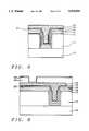
- FIGS. 1 through 5schematically illustrate in cross-sectional representation one preferred embodiment of this invention.
- FIGS. 6 through 8schematically illustrate in cross-sectional representation a second preferred embodiment of this invention.
- the semiconductor substrate 10is preferably composed of monocrystalline silicon.
- LPCVDlow pressure chemical vapor deposition
- APCVDatmospheric pressure chemical vapor deposition
- PECVDplasma-enhanced chemical vapor deposition
- a pattern of contact openingsare formed through the insulating structure to the semiconductor substrate 10 wherein there may be device regions formed therein as is well understood by those skilled in the art. Conventional lithography and etching techniques are used to form this pattern of openings. For simplicity, a single opening is shown in the Figs. and device regions in the semiconductor substrate are not shown, since they do not form a part of the invention.
- a barrier metal layeris sputtered over the surface of the substrate and within the contact openings.
- a collimatoris used during this sputtering so that most of the barrier metal coats the bottom of the opening and only a thin layer is formed on the sides of the contact openings.
- the barrier metal layeris be made up of multilayers.
- the first layer 13is composed of titanium and is between about 50 to 300 Angstroms thick.
- the second layer 14is composed of either titanium nitride or titanium tungsten and is between about 300 to 2000 Angstroms thick, and preferably between 750 and 2000 Angstroms thick. This second barrier metal layer prevents junction leakage.
- a final layer 15 of titaniumbetween about 300 to 800 Angstroms in thickness is deposited to complete the barrier metal layer.
- the top titanium layer 15overcomes the silicon nodule formation at the interface of the titanium nitride and the aluminum layers. It may be that the silicon and titanium combine to take away the possibility of silicon nodules forming.
- a first cold sputtering 16is performed.
- the preferred metalis aluminum or an aluminum alloy, such as AL 1% Si 0.5% Cu, is used.
- Alternative alloysare AL 0.5% Cu, AL 1% Cu, AL 1% Si, AL 2% Si, and the like.
- the cold deposition rateshould be as high as possible at more than about 150 Angstroms/sec and preferably more than about 180 Angstroms/sec to assure deposition at a temperature of less than about 150° C. and to assure a full and continuous film in the contact openings. It is preferred to operate at less than about 25° C. If the temperature rises above about 150° C., the aluminum becomes mobile and nucleates in small areas causing the continuous film to be lost. Little or no argon gas is used during the cold sputtering deposition.
- a hot deposition 18(shown in FIG. 3) immediately follows the cold deposition.
- a multi-chamber sputterersuch as a Varian M2000/8 sputtering system machine made by the Varian Corporation, 3075 Hansen Way M/S K-227, Palo Alto, Calif. 94303-1025, is used so that there is no interruption to move the wafer in and out of the sputterer.
- Argonis used as the heating gas during the hot sputtering step in the preferred sputtering machine.
- the chamberis heated to between about 500° to 550° C. After cold sputtering, the wafer is moved into the already heated hot sputtering chamber and hot sputtering commences immediately.
- only one chambercould be used for both the cold and hot sputtering.
- the backside Argon gascould be turned off so that the wafer is cool for the cold sputtering, the backside Argon gas is turned on and the hot sputtering proceeds.
- the collimatoris not used during the cold and hot metal sputtering steps, but only during the barrier metal formation step.
- the hot deposition rateshould be as low as possible, less than about 50 Angstroms/sec and preferably less than 20 Angstroms/sec. When hot sputtering begins, the void 20 is formed. This low deposition rate will cause the void 20 to be removed by surface tension.
- a titanium-aluminum alloy 22is formed between the cold deposited aluminum and the titanium layer 14.
- a high surface energyresults in a small surface area.
- the surface energy of the titanium-aluminum alloy 22is higher than the surface energy of the aluminum alloy 16, 18. Therefore, the surface area of the titanium-aluminum alloy 22 becomes smaller and smaller during the process and disappears at the final step; that is, the void 20 disappears.
- the void 20has been reduced in size. It is critical that the temperature must remain above about 500° C. during the hot deposition; otherwise the void will not be removed completely.
- the contact openinghas been filled completely and the void removed.
- the resulting metallizationhas an aluminum grain size of as much as 3 to 5 micrometers which will not cause problems for the resulting device.
- the following tableindicates the range of thicknesses of the cold and hot aluminum that would be required for various feature sizes.
- the thicknessis dependent upon the aspect ratio. For example, for a feature size of 0.6 microns, a shallow contact may require about 3000 Angstroms thickness of hot aluminum, while a very deep contact (e.g., 1.6 micrometers high by 0.4 micrometers wide) may require about 6000 Angstroms thickness of hot aluminum.
- the hot deposition process temperatureis also dependent on the aspect ratio, although higher than 500° C. is preferred.
- the metallization processcan be used to make multilevel interconnections; that is, second, third, etc., levels of metal connected to one another.
- FIG. 6the first metallization has been completed as described above for the first embodiment.
- the first metal layer 16, 18(cold and hot sputtered aluminum, respectively) has been patterned and a second insulating layer 26 has been deposited over the surface of the substrate.
- a contact or via openinghas been made through the second insulating layer 26 to the first metal layer 16, 18.
- a barrier metal layer 28is sputter deposited over the surface of the substrate and within the contact opening. This barrier metal layer consists only of titanium deposited to a thickness of between about 500 to 2000 Angstroms.
- This barrier metal layeris used for wetting; to promote adherence of the new metal layer to the metal exposed within the contact opening.
- a collimatormay or may not be used in this embodiment.
- the problem of silicon nodulesdoes not exist in this embodiment because of the titanium-aluminum alloy formation.
- cold sputtered aluminum 30is deposited at a temperature of less than about 150° C. and preferably less than about 25° C. as described above for the first embodiment.
- the high deposition rateis as above.
- the processcontinues as in the first embodiment with the hot sputtered aluminum 32 and the formation of the aluminum-titanium alloy 34 at the titanium/cold aluminum interface.
- FIG. 8shows the completed void free structure.
- the contact or via 30, 32 to electrically contact metal contact 16, 18can be made anywhere a 16, 18 metal line is present on layer 12.
- the metallization process of the present inventioncan be used for all levels of metallization and results in a good step coverage filling of contact openings, even those with high aspect ratios, with the absence of voids.
Landscapes
- Engineering & Computer Science (AREA)
- Physics & Mathematics (AREA)
- Condensed Matter Physics & Semiconductors (AREA)
- General Physics & Mathematics (AREA)
- Computer Hardware Design (AREA)
- Microelectronics & Electronic Packaging (AREA)
- Power Engineering (AREA)
- Manufacturing & Machinery (AREA)
- Internal Circuitry In Semiconductor Integrated Circuit Devices (AREA)
- Electrodes Of Semiconductors (AREA)
- Physical Vapour Deposition (AREA)
Abstract
Description
(1) Field of the Invention
The invention relates to a method of metallization of an integrated circuit device, and more particularly, to a metallization method with good step coverage in the manufacture of an integrated circuit device.
(2) Description of the Prior Art
In the fabrication of integrated circuit devices, metal layers make contact to lower conductive layers of the integrated circuit through vias in an insulating layer. Aluminum is often used as the interconnection metal. However, the sputtering process used to apply the aluminum often results in incomplete filling of the via openings. Large aluminum grains tend to form on the surface of the insulating layer within the via openings, causing voids.
Differing temperatures and deposition rates have been used to try to overcome the problem of voids. U.S. Pat. Nos. 4,994,162 to Armstrong et al and 5,108,951 to Chen et al describe such methods.
A principal object of the present invention is to provide an effective and very manufacturable method of metallization in the manufacture of an integrated circuit which prevents the formation of voids.
In accordance with the objects of this invention a new method of metallization of an integrated circuit is achieved. This method can be used for a first metallization to contact the semiconductor substrate regions or for a subsequent metallizations for interconnection within the integrated circuit. An insulating layer is provided over the surface of a semiconductor substrate or over a metallization layer. At least one contact opening is made through the insulating layer to the semiconductor substrate or to the metallization layer. A barrier metal layer is deposited over the surface of the substrate and within the contact opening wherein most of the barrier metal is deposited on the bottom of the contact opening rather than on the sides of the opening. A metal layer is cold sputtered over the barrier metal layer, then the metal is hot sputtered over the cold-sputtered metal layer wherein the cold and hot sputtering are continuous operations to complete the metallization of the integrated circuit.
In the accompanying drawings forming a material part of this description, there is shown:
FIGS. 1 through 5 schematically illustrate in cross-sectional representation one preferred embodiment of this invention.
FIGS. 6 through 8 schematically illustrate in cross-sectional representation a second preferred embodiment of this invention.
Referring now to FIG. 1, there is shown a portion of a partially completed integrated circuit. Thesemiconductor substrate 10 is preferably composed of monocrystalline silicon. Aninsulating layer 12, preferably composed of TEOS oxide, borophosphosilicate glass (BPSG), or the like, is deposited by low pressure chemical vapor deposition (LPCVD), atmospheric pressure chemical vapor deposition (APCVD), or plasma-enhanced chemical vapor deposition (PECVD) to a thickness of between about 4000 to 10,000 Angstroms.
A pattern of contact openings are formed through the insulating structure to thesemiconductor substrate 10 wherein there may be device regions formed therein as is well understood by those skilled in the art. Conventional lithography and etching techniques are used to form this pattern of openings. For simplicity, a single opening is shown in the Figs. and device regions in the semiconductor substrate are not shown, since they do not form a part of the invention.
A barrier metal layer is sputtered over the surface of the substrate and within the contact openings. A collimator is used during this sputtering so that most of the barrier metal coats the bottom of the opening and only a thin layer is formed on the sides of the contact openings. The barrier metal layer is be made up of multilayers. Thefirst layer 13 is composed of titanium and is between about 50 to 300 Angstroms thick. Thesecond layer 14 is composed of either titanium nitride or titanium tungsten and is between about 300 to 2000 Angstroms thick, and preferably between 750 and 2000 Angstroms thick. This second barrier metal layer prevents junction leakage. Afinal layer 15 of titanium between about 300 to 800 Angstroms in thickness is deposited to complete the barrier metal layer. Thetop titanium layer 15 overcomes the silicon nodule formation at the interface of the titanium nitride and the aluminum layers. It may be that the silicon and titanium combine to take away the possibility of silicon nodules forming.
There is a cool down period, followed by the metal deposition, now to be described. Referring now to FIG. 2, a firstcold sputtering 16 is performed. The preferred metal is aluminum or an aluminum alloy, such as AL 1% Si 0.5% Cu, is used. Alternative alloys are AL 0.5% Cu, AL 1% Cu, AL 1% Si, AL 2% Si, and the like. The cold deposition rate should be as high as possible at more than about 150 Angstroms/sec and preferably more than about 180 Angstroms/sec to assure deposition at a temperature of less than about 150° C. and to assure a full and continuous film in the contact openings. It is preferred to operate at less than about 25° C. If the temperature rises above about 150° C., the aluminum becomes mobile and nucleates in small areas causing the continuous film to be lost. Little or no argon gas is used during the cold sputtering deposition.
A hot deposition 18 (shown in FIG. 3) immediately follows the cold deposition. A multi-chamber sputterer, such as a Varian M2000/8 sputtering system machine made by the Varian Corporation, 3075 Hansen Way M/S K-227, Palo Alto, Calif. 94303-1025, is used so that there is no interruption to move the wafer in and out of the sputterer. Argon is used as the heating gas during the hot sputtering step in the preferred sputtering machine. The chamber is heated to between about 500° to 550° C. After cold sputtering, the wafer is moved into the already heated hot sputtering chamber and hot sputtering commences immediately. Alternatively, only one chamber could be used for both the cold and hot sputtering. The backside Argon gas could be turned off so that the wafer is cool for the cold sputtering, the backside Argon gas is turned on and the hot sputtering proceeds. The collimator is not used during the cold and hot metal sputtering steps, but only during the barrier metal formation step.
The hot deposition rate should be as low as possible, less than about 50 Angstroms/sec and preferably less than 20 Angstroms/sec. When hot sputtering begins, thevoid 20 is formed. This low deposition rate will cause thevoid 20 to be removed by surface tension.
Referring now to FIG. 4, a titanium-aluminum alloy 22 is formed between the cold deposited aluminum and thetitanium layer 14. A high surface energy results in a small surface area. The surface energy of the titanium-aluminum alloy 22 is higher than the surface energy of thealuminum alloy aluminum alloy 22 becomes smaller and smaller during the process and disappears at the final step; that is, thevoid 20 disappears. In FIG. 4, thevoid 20 has been reduced in size. It is critical that the temperature must remain above about 500° C. during the hot deposition; otherwise the void will not be removed completely. Referring now to FIG. 5, the contact opening has been filled completely and the void removed. The resulting metallization has an aluminum grain size of as much as 3 to 5 micrometers which will not cause problems for the resulting device.
The following Example is given to show the important features of the invention and to aid in the understanding thereof and variations may be made by one skilled in the art without departing from the spirit and scope of the invention.
The following table indicates the range of thicknesses of the cold and hot aluminum that would be required for various feature sizes.
TABLE 1 ______________________________________ Feature size Cold AL thickness Hot Al Thickness (in microns) (in Angstroms) (in Angstroms) ______________________________________ 0.8 2000-4000 2500-7000 0.6 2000-4000 2500-7000 0.5 2000-4000 2500-7000 0.3 1500-3000 2500-7000 ______________________________________
The thickness is dependent upon the aspect ratio. For example, for a feature size of 0.6 microns, a shallow contact may require about 3000 Angstroms thickness of hot aluminum, while a very deep contact (e.g., 1.6 micrometers high by 0.4 micrometers wide) may require about 6000 Angstroms thickness of hot aluminum. The hot deposition process temperature is also dependent on the aspect ratio, although higher than 500° C. is preferred.
In the second preferred embodiment of the present invention shown in FIGS. 6 to 8, the metallization process can be used to make multilevel interconnections; that is, second, third, etc., levels of metal connected to one another. Referring now to FIG. 6, the first metallization has been completed as described above for the first embodiment. Thefirst metal layer 16, 18 (cold and hot sputtered aluminum, respectively) has been patterned and a second insulatinglayer 26 has been deposited over the surface of the substrate. A contact or via opening has been made through the second insulatinglayer 26 to thefirst metal layer barrier metal layer 28 is sputter deposited over the surface of the substrate and within the contact opening. This barrier metal layer consists only of titanium deposited to a thickness of between about 500 to 2000 Angstroms. This barrier metal layer is used for wetting; to promote adherence of the new metal layer to the metal exposed within the contact opening. A collimator may or may not be used in this embodiment. The problem of silicon nodules does not exist in this embodiment because of the titanium-aluminum alloy formation.
Referring now to FIG. 7, cold sputteredaluminum 30 is deposited at a temperature of less than about 150° C. and preferably less than about 25° C. as described above for the first embodiment. The high deposition rate is as above. The process continues as in the first embodiment with the hot sputteredaluminum 32 and the formation of the aluminum-titanium alloy 34 at the titanium/cold aluminum interface. FIG. 8 shows the completed void free structure. As is understood by those skilled in the art, the contact or via 30, 32 to electricallycontact metal contact layer 12.
The metallization process of the present invention can be used for all levels of metallization and results in a good step coverage filling of contact openings, even those with high aspect ratios, with the absence of voids.
While the invention has been particularly shown and described with reference to the preferred embodiments thereof, it will be understood by those skilled in the art that various changes in form and details may be made without departing from the spirit and scope of the invention.
Claims (29)
1. The method of metallization of an integrated circuit comprising:
providing an insulating layer over the surface of a semiconductor substrate;
providing at least one contact opening through said insulating layer to said semiconductor substrate;
depositing a barrier metal layer over the surface of said substrate and within said contact opening wherein most of said barrier metal is deposited on the bottom of said contact opening rather than on the sides of said opening;
cold sputtering an aluminum layer over said barrier metal layer at a temperature of less than about 150° C. and a deposition rate of more than about 180 Angstroms/sec.; and
hot sputtering an aluminum layer over said cold-sputtered layer at a temperature of more than about 500° C. and at a deposition rate of less than about 50 Angstroms/sec. wherein said cold and hot sputtering are continuous operations to complete said metallization of said integrated circuit.
2. The method of claim 1 wherein said insulating layer is composed of silicon dioxide deposited to a thickness of between about 4000 to 10,000 Angstroms.
3. The method of claim 1 wherein said barrier metal layer is composed of a multilayer of titanium, titanium nitride, and titanium and wherein a collimator is used in sputtering this multilayer so that most of said multilayer is deposited on the bottom of said contact opening rather than on the sidewalls of said opening.
4. The method of claim 3 wherein the thicknesses of said multilayer are between about 50 to 300 Angstroms of titanium, 750 to 2000 Angstroms of titanium nitride, and 300 to 800 Angstroms of titanium.
5. The method of claim 1 wherein said cold sputtering of said aluminum layer is performed at a temperature of between about 20° and 150° C.
6. The method of claim 1 wherein said cold sputtering of said aluminum layer is performed at a high deposition rate of more than about 150 Angstroms/sec so as to assure a full and continuous film within said contact opening.
7. The method of claim 1 wherein said hot sputtering of said aluminum layer is performed at a temperature of between about 500° to 550° C.
8. The method of claim 1 wherein said hot sputtering of said aluminum layer is performed at a very low deposition rate of less than about 20 Angstroms/sec.
9. The method of claim 8 wherein said hot sputtering of said aluminum layer at a very low deposition rate causes no void to be formed within said contact opening.
10. The method of claim 8 wherein said hot sputtering of said aluminum layer at a very low deposition rate causes the formation of an alloy between said cold sputtered aluminum layer and said barrier metal layer wherein said alloy prevents formation of a void within said contact opening.
11. The method of metallization of an integrated circuit comprising:
providing a first insulating layer over the surface of a semiconductor substrate;
providing at least a first metallization layer over said insulating layer;
providing a second insulating layer over the surface of said first metallization layer;
providing at least one contact opening through said second insulating layer to said first metallization layer;
depositing a barrier metal layer composed of titanium over the surface of said substrate and within said contact opening wherein most of said barrier metal is deposited on the bottom of said contact opening rather than on the sides of said opening by a collimator process;
cold sputtering an aluminum layer over said barrier metal layer at a temperature of less than about 150° C. and a deposition rate of more than about 180 Angstroms/sec.; and
hot sputtering an aluminum layer over said cold-sputtered layer at a temperature of more than about 500° C. and at a deposition rate of less than about 50 Angstroms/sec. wherein said cold and hot sputtering are continuous operations to complete said metallization of said integrated circuit.
12. The method of claim 11 wherein said barrier metal layer is composed of titanium, titanium nitride and titanium.
13. The method of claim 11 wherein the thicknesses of said barrier layer is between about 500 to 2000 Angstroms.
14. The method of claim 11 wherein said cold sputtering of said aluminum layer is performed at a high deposition rate of more than about 150 Angstroms/sec so as to assure a full and continuous film within said contact opening.
15. The method of claim 11 wherein said hot sputtering of said aluminum layer is performed at a temperature of between about 500° to 550° C.
16. The method of claim 11 wherein said hot sputtering of said aluminum layer is performed at a low deposition rate of less than about 20 Angstroms/sec.
17. The method of claim 16 wherein said hot sputtering of said aluminum layer at a low deposition rate causes no void to be formed within said contact opening.
18. The method of claim 16 wherein said hot sputtering of said aluminum layer at a low deposition rate causes the formation of an alloy between said cold sputtered aluminum layer and said barrier metal layer wherein said alloy prevents formation of a void within said contact opening.
19. The method of metallization of an integrated circuit comprising:
providing an insulating layer over a conducting layer on a semiconductor substrate;
providing at least one contact opening through said insulating layer to said conducting layer;
depositing a barrier metal layer composed of titanium over the surface of said substrate and within said contact opening wherein most of said barrier metal is deposited on the bottom of said contact opening rather than on the sides of said opening by a collimator process:
cold sputtering an aluminum layer over said barrier metal layer at a temperature of less than about 150° C. and a deposition rate of more than about 180 Angstroms/sec.; and
hot sputtering an aluminum layer over said cold-sputtered layer at a temperature of more than about 500° C. and at a deposition rate of less than about 50 Angstroms/sec. wherein said cold and hot sputtering are continuous operations to complete said metallization of said integrated circuit.
20. The method of claim 19 wherein said conducting layer is said semiconductor substrate.
21. The method of claim 20 wherein said barrier metal layer is composed of a multilayer of titanium, titanium nitride, and titanium.
22. The method of claim 21 wherein the thicknesses of said multilayer are between about 50 to 300 Angstroms of titanium, 750 to 2000 Angstroms of titanium nitride, and 300 to 800 Angstroms of titanium.
23. The method of claim 19 wherein said conducting layer is at least a first metallization layer over a first insulating layer over said semiconductor substrate.
24. The method of claim 23 wherein the thicknesses of said barrier layer is between about 500 to 2000 Angstroms.
25. The method of claim 19 wherein said cold sputtering of said aluminum layer is performed at a temperature of between about 20° to 150° C.
26. The method of claim 19 wherein said hot sputtering of said aluminum layer is performed at a temperature of between about 500° to 550° C.
27. The method of claim 19 wherein said hot sputtering of said aluminum layer is performed at a low deposition rate of less than about 20 Angstroms/sec.
28. The method of claim 27 wherein said hot sputtering of said aluminum layer at a low deposition rate causes no void to be formed within said contact opening.
29. The method of claim 27 wherein said hot sputtering of said aluminum layer at a very low deposition rate causes the formation of an alloy between said cold sputtered aluminum layer and said barrier metal layer wherein said alloy prevents formation of a void within said contact opening.
Priority Applications (5)
| Application Number | Priority Date | Filing Date | Title |
|---|---|---|---|
| US08/108,224US5356836A (en) | 1993-08-19 | 1993-08-19 | Aluminum plug process |
| DE4400726ADE4400726A1 (en) | 1993-08-19 | 1994-01-13 | Metal vapor deposition method on an integrated circuit device |
| FR9402273AFR2709207B1 (en) | 1993-08-19 | 1994-02-28 | Metallization process of an integrated circuit. |
| JP6034491AJPH0766205A (en) | 1993-08-19 | 1994-03-04 | Integrated circuit metallization method |
| KR1019940009138AKR100291284B1 (en) | 1993-08-19 | 1994-04-28 | Aluminum metal layer wiring method |
Applications Claiming Priority (1)
| Application Number | Priority Date | Filing Date | Title |
|---|---|---|---|
| US08/108,224US5356836A (en) | 1993-08-19 | 1993-08-19 | Aluminum plug process |
Publications (1)
| Publication Number | Publication Date |
|---|---|
| US5356836Atrue US5356836A (en) | 1994-10-18 |
Family
ID=22320980
Family Applications (1)
| Application Number | Title | Priority Date | Filing Date |
|---|---|---|---|
| US08/108,224Expired - LifetimeUS5356836A (en) | 1993-08-19 | 1993-08-19 | Aluminum plug process |
Country Status (5)
| Country | Link |
|---|---|
| US (1) | US5356836A (en) |
| JP (1) | JPH0766205A (en) |
| KR (1) | KR100291284B1 (en) |
| DE (1) | DE4400726A1 (en) |
| FR (1) | FR2709207B1 (en) |
Cited By (54)
| Publication number | Priority date | Publication date | Assignee | Title |
|---|---|---|---|---|
| US5449639A (en)* | 1994-10-24 | 1995-09-12 | Taiwan Semiconductor Manufacturing Company Ltd. | Disposable metal anti-reflection coating process used together with metal dry/wet etch |
| US5488014A (en)* | 1990-08-28 | 1996-01-30 | Mitsubishi Denki Kabushiki Kaisha | Interconnection structure of semiconductor integrated circuit device and manufacturing method thererfor |
| US5523259A (en)* | 1994-12-05 | 1996-06-04 | At&T Corp. | Method of forming metal layers formed as a composite of sub-layers using Ti texture control layer |
| US5543357A (en)* | 1993-12-08 | 1996-08-06 | Nec Corporation | Process of manufacturing a semiconductor device by filling a via hole in an interlayered film of the device with wiring metal |
| US5580823A (en)* | 1994-12-15 | 1996-12-03 | Motorola, Inc. | Process for fabricating a collimated metal layer and contact structure in a semiconductor device |
| US5585308A (en)* | 1993-12-23 | 1996-12-17 | Sgs-Thomson Microelectronics, Inc. | Method for improved pre-metal planarization |
| US5599749A (en)* | 1994-10-21 | 1997-02-04 | Yamaha Corporation | Manufacture of micro electron emitter |
| US5604155A (en)* | 1995-07-17 | 1997-02-18 | Winbond Electronics Corp. | Al-based contact formation process using Ti glue layer to prevent nodule-induced bridging |
| US5633199A (en)* | 1995-11-02 | 1997-05-27 | Motorola Inc. | Process for fabricating a metallized interconnect structure in a semiconductor device |
| US5677238A (en)* | 1996-04-29 | 1997-10-14 | Chartered Semiconductor Manufacturing Pte Ltd | Semiconductor contact metallization |
| US5702983A (en)* | 1993-11-02 | 1997-12-30 | Sony Corporation | Method for manufacturing a semiconductor device with a metallic interconnection layer |
| US5712194A (en)* | 1991-02-12 | 1998-01-27 | Matsushita Electronics Corporation | Semiconductor device including interlayer dielectric film layers and conductive film layers |
| US5719446A (en)* | 1993-06-21 | 1998-02-17 | Sony Corporation | Multilayer interconnect structure for semiconductor device and method of manufacturing same |
| US5747360A (en)* | 1993-09-17 | 1998-05-05 | Applied Materials, Inc. | Method of metalizing a semiconductor wafer |
| US5750439A (en)* | 1995-03-29 | 1998-05-12 | Yamaha Corporation | Method of making aluminum alloy wiring with less silicon nodule |
| EP0766302A3 (en)* | 1995-09-27 | 1998-05-13 | Motorola, Inc. | Process for fabricating a CVD aluminium layer in a semiconductor device |
| EP0790646A3 (en)* | 1996-02-15 | 1998-06-03 | Nec Corporation | Method of forming a wiring layer filling a contact hole |
| US5776831A (en)* | 1995-12-27 | 1998-07-07 | Lsi Logic Corporation | Method of forming a high electromigration resistant metallization system |
| US5798300A (en)* | 1995-07-07 | 1998-08-25 | Lucent Technologies Inc. | Method for forming conductors in integrated circuits |
| US5804251A (en)* | 1995-12-29 | 1998-09-08 | Intel Corporation | Low temperature aluminum alloy plug technology |
| US5846877A (en)* | 1995-05-27 | 1998-12-08 | Lg Semicon Co., Ltd. | Method for fabricating an Al-Ge alloy wiring of semiconductor device |
| US5851915A (en)* | 1993-11-30 | 1998-12-22 | Nec Corporation | Method of manufacturing a semiconductor device through a reduced number of simple processes at a relatively low cost |
| US5851923A (en)* | 1996-01-18 | 1998-12-22 | Micron Technology, Inc. | Integrated circuit and method for forming and integrated circuit |
| US5883002A (en)* | 1996-08-29 | 1999-03-16 | Winbond Electronics Corp. | Method of forming contact profile by improving TEOS/BPSG selectivity for manufacturing a semiconductor device |
| EP0877424A3 (en)* | 1997-04-16 | 1999-09-15 | STMicroelectronics, Inc. | Interconnect method and structure for semiconductor devices |
| US5985746A (en)* | 1996-11-21 | 1999-11-16 | Lsi Logic Corporation | Process for forming self-aligned conductive plugs in multiple insulation levels in integrated circuit structures and resulting product |
| US5994213A (en)* | 1998-02-09 | 1999-11-30 | Taiwan Semiconductor Manufacturing Company, Ltd. | Aluminum plug process |
| US5994206A (en)* | 1997-10-06 | 1999-11-30 | Advanced Micro Devices, Inc. | Method of forming a high conductivity metal interconnect using metal gettering plug and system performing the method |
| KR20000004358A (en)* | 1998-06-30 | 2000-01-25 | 김영환 | Interconnect layer structure of semiconductor device |
| EP0951066A4 (en)* | 1996-12-12 | 2000-02-23 | Asahi Chemical Ind | Method of manufacturing semiconductor device |
| US6080657A (en)* | 1999-07-16 | 2000-06-27 | Taiwan Semiconductor Manufacturing Company | Method of reducing AlCu hillocks |
| US6083823A (en)* | 1996-06-28 | 2000-07-04 | International Business Machines Corporation | Metal deposition process for metal lines over topography |
| US6100182A (en)* | 1997-06-23 | 2000-08-08 | Hyundai Electronics Industries, Co., Ltd. | Method for forming metal interconnection of semiconductor device |
| US6130156A (en)* | 1998-04-01 | 2000-10-10 | Texas Instruments Incorporated | Variable doping of metal plugs for enhanced reliability |
| US6150252A (en)* | 1995-05-23 | 2000-11-21 | Texas Instruments Incorporated | Multi-stage semiconductor cavity filling process |
| US6184120B1 (en)* | 1996-12-06 | 2001-02-06 | Nec Corporation | Method of forming a buried plug and an interconnection |
| US6207568B1 (en)* | 1998-11-27 | 2001-03-27 | Taiwan Semiconductor Manufacturing Company | Ionized metal plasma (IMP) method for forming (111) oriented aluminum containing conductor layer |
| US6300237B1 (en)* | 1995-01-11 | 2001-10-09 | Hitachi Ltd. | Semiconductor integrated circuit device and method for making the same |
| US6335569B1 (en)* | 1995-01-03 | 2002-01-01 | International Business Machines Corporation | Soft metal conductor and method of making |
| US6365514B1 (en) | 1997-12-23 | 2002-04-02 | Intel Corporation | Two chamber metal reflow process |
| US6440841B2 (en)* | 1999-03-11 | 2002-08-27 | United Microelectronics Corp. | Method of fabricating vias |
| US20030042133A1 (en)* | 2001-08-28 | 2003-03-06 | Jae-Wook Lee | Method for depositing a metal barrier layer |
| US6627542B1 (en)* | 1999-07-12 | 2003-09-30 | Applied Materials, Inc. | Continuous, non-agglomerated adhesion of a seed layer to a barrier layer |
| US6720253B2 (en)* | 1997-12-26 | 2004-04-13 | Kabushiki Kaisha Toshiba | Method of manufacturing semiconductor device having an aluminum wiring layer |
| US6747354B2 (en)* | 2002-02-27 | 2004-06-08 | Samsung Electronics Co., Ltd. | Semiconductor devices having multilevel interconnections and methods for manufacturing the same |
| US6759324B1 (en)* | 1998-09-02 | 2004-07-06 | Micron Technology Inc | Method of forming a low resistance contact to underlying aluminum interconnect by depositing titanium in a via opening and reacting the titanium with the aluminum |
| US20040180541A1 (en)* | 2002-01-18 | 2004-09-16 | International Business Machines Corporation | Soft metal conductor and method of making |
| US20050112794A1 (en)* | 2003-11-20 | 2005-05-26 | International Business Machines Corporation | Improved bond pad |
| US20110097897A1 (en)* | 2009-10-23 | 2011-04-28 | Elpida Memory, Inc | Method for manufacturing semiconductor device |
| US20150028490A1 (en)* | 2013-07-25 | 2015-01-29 | Globalfoundries Singapore Pte. Ltd. | Integrated circuits having device contacts and methods for fabricating the same |
| US20150243535A1 (en)* | 2014-02-21 | 2015-08-27 | Sts Semiconductor & Telecommunications Co., Ltd. | Cluster type semiconductor processing apparatus and method for manufacturing semiconductor device using the same |
| US20170287774A1 (en)* | 2016-03-29 | 2017-10-05 | Renesas Electronics Corporation | Semiconductor device and method for manufacturing the same |
| CN116397205A (en)* | 2023-03-30 | 2023-07-07 | 华虹半导体(无锡)有限公司 | Hot aluminum process method for avoiding edge damage of electrostatic chuck |
| CN119170566A (en)* | 2024-10-29 | 2024-12-20 | 无锡邑文微电子科技股份有限公司 | A method for hot aluminum hole filling and a sputtering device |
Citations (9)
| Publication number | Priority date | Publication date | Assignee | Title |
|---|---|---|---|---|
| EP0168828A2 (en)* | 1984-07-18 | 1986-01-22 | Hitachi, Ltd. | Method for manufacturing a semiconductor device having wiring layers |
| US4837183A (en)* | 1988-05-02 | 1989-06-06 | Motorola Inc. | Semiconductor device metallization process |
| JPH01160036A (en)* | 1987-12-17 | 1989-06-22 | Oki Electric Ind Co Ltd | Semiconductor device |
| US4960732A (en)* | 1987-02-19 | 1990-10-02 | Advanced Micro Devices, Inc. | Contact plug and interconnect employing a barrier lining and a backfilled conductor material |
| US4994162A (en)* | 1989-09-29 | 1991-02-19 | Materials Research Corporation | Planarization method |
| US5007372A (en)* | 1987-12-04 | 1991-04-16 | Research Development Corporation | Vacuum depositing apparatus |
| US5106781A (en)* | 1988-07-12 | 1992-04-21 | U.S. Philips Corporation | Method of establishing an interconnection level on a semiconductor device having a high integration density |
| US5108951A (en)* | 1990-11-05 | 1992-04-28 | Sgs-Thomson Microelectronics, Inc. | Method for forming a metal contact |
| US5240880A (en)* | 1992-05-05 | 1993-08-31 | Zilog, Inc. | Ti/TiN/Ti contact metallization |
Family Cites Families (6)
| Publication number | Priority date | Publication date | Assignee | Title |
|---|---|---|---|---|
| DE69031903T2 (en)* | 1989-11-30 | 1998-04-16 | Sgs Thomson Microelectronics | Process for making interlayer contacts |
| KR100228259B1 (en)* | 1990-10-24 | 1999-11-01 | 고지마 마따오 | Thin film formation method and semiconductor device |
| KR920010620A (en)* | 1990-11-30 | 1992-06-26 | 원본미기재 | How to Form Aluminum Stacked Contacts / Pathways for Multi-layer Interconnect Lines |
| JPH07109030B2 (en)* | 1991-02-12 | 1995-11-22 | アプライド マテリアルズ インコーポレイテッド | Method for sputtering aluminum layer on semiconductor wafer |
| JP2725944B2 (en)* | 1991-04-19 | 1998-03-11 | インターナショナル・ビジネス・マシーンズ・コーポレイション | Metal layer deposition method |
| EP0514103A1 (en)* | 1991-05-14 | 1992-11-19 | STMicroelectronics, Inc. | Barrier metal process for sub-micron contacts |
- 1993
- 1993-08-19USUS08/108,224patent/US5356836A/ennot_activeExpired - Lifetime
- 1994
- 1994-01-13DEDE4400726Apatent/DE4400726A1/ennot_activeWithdrawn
- 1994-02-28FRFR9402273Apatent/FR2709207B1/ennot_activeExpired - Fee Related
- 1994-03-04JPJP6034491Apatent/JPH0766205A/enactivePending
- 1994-04-28KRKR1019940009138Apatent/KR100291284B1/ennot_activeExpired - Lifetime
Patent Citations (9)
| Publication number | Priority date | Publication date | Assignee | Title |
|---|---|---|---|---|
| EP0168828A2 (en)* | 1984-07-18 | 1986-01-22 | Hitachi, Ltd. | Method for manufacturing a semiconductor device having wiring layers |
| US4960732A (en)* | 1987-02-19 | 1990-10-02 | Advanced Micro Devices, Inc. | Contact plug and interconnect employing a barrier lining and a backfilled conductor material |
| US5007372A (en)* | 1987-12-04 | 1991-04-16 | Research Development Corporation | Vacuum depositing apparatus |
| JPH01160036A (en)* | 1987-12-17 | 1989-06-22 | Oki Electric Ind Co Ltd | Semiconductor device |
| US4837183A (en)* | 1988-05-02 | 1989-06-06 | Motorola Inc. | Semiconductor device metallization process |
| US5106781A (en)* | 1988-07-12 | 1992-04-21 | U.S. Philips Corporation | Method of establishing an interconnection level on a semiconductor device having a high integration density |
| US4994162A (en)* | 1989-09-29 | 1991-02-19 | Materials Research Corporation | Planarization method |
| US5108951A (en)* | 1990-11-05 | 1992-04-28 | Sgs-Thomson Microelectronics, Inc. | Method for forming a metal contact |
| US5240880A (en)* | 1992-05-05 | 1993-08-31 | Zilog, Inc. | Ti/TiN/Ti contact metallization |
Cited By (70)
| Publication number | Priority date | Publication date | Assignee | Title |
|---|---|---|---|---|
| US5488014A (en)* | 1990-08-28 | 1996-01-30 | Mitsubishi Denki Kabushiki Kaisha | Interconnection structure of semiconductor integrated circuit device and manufacturing method thererfor |
| US5712194A (en)* | 1991-02-12 | 1998-01-27 | Matsushita Electronics Corporation | Semiconductor device including interlayer dielectric film layers and conductive film layers |
| US5719446A (en)* | 1993-06-21 | 1998-02-17 | Sony Corporation | Multilayer interconnect structure for semiconductor device and method of manufacturing same |
| US5904562A (en)* | 1993-09-17 | 1999-05-18 | Applied Materials, Inc. | Method of metallizing a semiconductor wafer |
| US5747360A (en)* | 1993-09-17 | 1998-05-05 | Applied Materials, Inc. | Method of metalizing a semiconductor wafer |
| US5702983A (en)* | 1993-11-02 | 1997-12-30 | Sony Corporation | Method for manufacturing a semiconductor device with a metallic interconnection layer |
| US5851915A (en)* | 1993-11-30 | 1998-12-22 | Nec Corporation | Method of manufacturing a semiconductor device through a reduced number of simple processes at a relatively low cost |
| US5543357A (en)* | 1993-12-08 | 1996-08-06 | Nec Corporation | Process of manufacturing a semiconductor device by filling a via hole in an interlayered film of the device with wiring metal |
| US5903054A (en)* | 1993-12-23 | 1999-05-11 | Stmicroelectronics, Inc. | Integrated circuit with improved pre-metal planarization |
| US5585308A (en)* | 1993-12-23 | 1996-12-17 | Sgs-Thomson Microelectronics, Inc. | Method for improved pre-metal planarization |
| US5599749A (en)* | 1994-10-21 | 1997-02-04 | Yamaha Corporation | Manufacture of micro electron emitter |
| US5449639A (en)* | 1994-10-24 | 1995-09-12 | Taiwan Semiconductor Manufacturing Company Ltd. | Disposable metal anti-reflection coating process used together with metal dry/wet etch |
| EP0716447A3 (en)* | 1994-12-05 | 1997-01-08 | At & T Corp | Metal layers formed as a composite of sub-layers and devices including same |
| US5523259A (en)* | 1994-12-05 | 1996-06-04 | At&T Corp. | Method of forming metal layers formed as a composite of sub-layers using Ti texture control layer |
| US5580823A (en)* | 1994-12-15 | 1996-12-03 | Motorola, Inc. | Process for fabricating a collimated metal layer and contact structure in a semiconductor device |
| US6335569B1 (en)* | 1995-01-03 | 2002-01-01 | International Business Machines Corporation | Soft metal conductor and method of making |
| US6300237B1 (en)* | 1995-01-11 | 2001-10-09 | Hitachi Ltd. | Semiconductor integrated circuit device and method for making the same |
| US20040235289A1 (en)* | 1995-01-11 | 2004-11-25 | Masayuki Suzuki | Semiconductor integrated circuit device and method for making the same |
| US6780757B2 (en) | 1995-01-11 | 2004-08-24 | Renesas Technology Corp. | Semiconductor integrated circuit device and method for making the same |
| US6538329B2 (en)* | 1995-01-11 | 2003-03-25 | Hitachi, Ltd. | Semiconductor integrated circuit device and method for making the same |
| US6583049B2 (en) | 1995-01-11 | 2003-06-24 | Hitachi, Ltd. | Semiconductor integrated circuit device and method for making the same |
| US5750439A (en)* | 1995-03-29 | 1998-05-12 | Yamaha Corporation | Method of making aluminum alloy wiring with less silicon nodule |
| US6150252A (en)* | 1995-05-23 | 2000-11-21 | Texas Instruments Incorporated | Multi-stage semiconductor cavity filling process |
| US5846877A (en)* | 1995-05-27 | 1998-12-08 | Lg Semicon Co., Ltd. | Method for fabricating an Al-Ge alloy wiring of semiconductor device |
| US5798300A (en)* | 1995-07-07 | 1998-08-25 | Lucent Technologies Inc. | Method for forming conductors in integrated circuits |
| US5604155A (en)* | 1995-07-17 | 1997-02-18 | Winbond Electronics Corp. | Al-based contact formation process using Ti glue layer to prevent nodule-induced bridging |
| EP0766302A3 (en)* | 1995-09-27 | 1998-05-13 | Motorola, Inc. | Process for fabricating a CVD aluminium layer in a semiconductor device |
| US5633199A (en)* | 1995-11-02 | 1997-05-27 | Motorola Inc. | Process for fabricating a metallized interconnect structure in a semiconductor device |
| US5776831A (en)* | 1995-12-27 | 1998-07-07 | Lsi Logic Corporation | Method of forming a high electromigration resistant metallization system |
| US5804251A (en)* | 1995-12-29 | 1998-09-08 | Intel Corporation | Low temperature aluminum alloy plug technology |
| US6107196A (en)* | 1996-01-18 | 2000-08-22 | Micron Technology, Inc. | Integrated circuit, and method for forming an integrated circuit |
| US5851923A (en)* | 1996-01-18 | 1998-12-22 | Micron Technology, Inc. | Integrated circuit and method for forming and integrated circuit |
| US5936308A (en)* | 1996-01-18 | 1999-08-10 | Micron Technology, Inc. | Interlocking conductive plug for use with an integrated circuit |
| US5985754A (en)* | 1996-02-15 | 1999-11-16 | Nec Corporation | Method of forming a void-free contact plug |
| EP0790646A3 (en)* | 1996-02-15 | 1998-06-03 | Nec Corporation | Method of forming a wiring layer filling a contact hole |
| US5677238A (en)* | 1996-04-29 | 1997-10-14 | Chartered Semiconductor Manufacturing Pte Ltd | Semiconductor contact metallization |
| US6083823A (en)* | 1996-06-28 | 2000-07-04 | International Business Machines Corporation | Metal deposition process for metal lines over topography |
| US5883002A (en)* | 1996-08-29 | 1999-03-16 | Winbond Electronics Corp. | Method of forming contact profile by improving TEOS/BPSG selectivity for manufacturing a semiconductor device |
| US5985746A (en)* | 1996-11-21 | 1999-11-16 | Lsi Logic Corporation | Process for forming self-aligned conductive plugs in multiple insulation levels in integrated circuit structures and resulting product |
| US6184120B1 (en)* | 1996-12-06 | 2001-02-06 | Nec Corporation | Method of forming a buried plug and an interconnection |
| EP0951066A4 (en)* | 1996-12-12 | 2000-02-23 | Asahi Chemical Ind | Method of manufacturing semiconductor device |
| US6162729A (en)* | 1996-12-12 | 2000-12-19 | Asahi Kasei Kogyo Kabushiki Kaisha | Method of manufacturing multiple aluminum layer in a semiconductor device |
| US6395629B1 (en) | 1997-04-16 | 2002-05-28 | Stmicroelectronics, Inc. | Interconnect method and structure for semiconductor devices |
| EP0877424A3 (en)* | 1997-04-16 | 1999-09-15 | STMicroelectronics, Inc. | Interconnect method and structure for semiconductor devices |
| US6100182A (en)* | 1997-06-23 | 2000-08-08 | Hyundai Electronics Industries, Co., Ltd. | Method for forming metal interconnection of semiconductor device |
| US5994206A (en)* | 1997-10-06 | 1999-11-30 | Advanced Micro Devices, Inc. | Method of forming a high conductivity metal interconnect using metal gettering plug and system performing the method |
| US6365514B1 (en) | 1997-12-23 | 2002-04-02 | Intel Corporation | Two chamber metal reflow process |
| US6720253B2 (en)* | 1997-12-26 | 2004-04-13 | Kabushiki Kaisha Toshiba | Method of manufacturing semiconductor device having an aluminum wiring layer |
| US5994213A (en)* | 1998-02-09 | 1999-11-30 | Taiwan Semiconductor Manufacturing Company, Ltd. | Aluminum plug process |
| US6130156A (en)* | 1998-04-01 | 2000-10-10 | Texas Instruments Incorporated | Variable doping of metal plugs for enhanced reliability |
| KR20000004358A (en)* | 1998-06-30 | 2000-01-25 | 김영환 | Interconnect layer structure of semiconductor device |
| US6759324B1 (en)* | 1998-09-02 | 2004-07-06 | Micron Technology Inc | Method of forming a low resistance contact to underlying aluminum interconnect by depositing titanium in a via opening and reacting the titanium with the aluminum |
| US6207568B1 (en)* | 1998-11-27 | 2001-03-27 | Taiwan Semiconductor Manufacturing Company | Ionized metal plasma (IMP) method for forming (111) oriented aluminum containing conductor layer |
| US6440841B2 (en)* | 1999-03-11 | 2002-08-27 | United Microelectronics Corp. | Method of fabricating vias |
| US6627542B1 (en)* | 1999-07-12 | 2003-09-30 | Applied Materials, Inc. | Continuous, non-agglomerated adhesion of a seed layer to a barrier layer |
| US6080657A (en)* | 1999-07-16 | 2000-06-27 | Taiwan Semiconductor Manufacturing Company | Method of reducing AlCu hillocks |
| US20030042133A1 (en)* | 2001-08-28 | 2003-03-06 | Jae-Wook Lee | Method for depositing a metal barrier layer |
| US20040180541A1 (en)* | 2002-01-18 | 2004-09-16 | International Business Machines Corporation | Soft metal conductor and method of making |
| US6943105B2 (en) | 2002-01-18 | 2005-09-13 | International Business Machines Corporation | Soft metal conductor and method of making |
| US6747354B2 (en)* | 2002-02-27 | 2004-06-08 | Samsung Electronics Co., Ltd. | Semiconductor devices having multilevel interconnections and methods for manufacturing the same |
| US20050112794A1 (en)* | 2003-11-20 | 2005-05-26 | International Business Machines Corporation | Improved bond pad |
| US7056820B2 (en) | 2003-11-20 | 2006-06-06 | International Business Machines Corporation | Bond pad |
| US20110097897A1 (en)* | 2009-10-23 | 2011-04-28 | Elpida Memory, Inc | Method for manufacturing semiconductor device |
| US20150028490A1 (en)* | 2013-07-25 | 2015-01-29 | Globalfoundries Singapore Pte. Ltd. | Integrated circuits having device contacts and methods for fabricating the same |
| US9941160B2 (en)* | 2013-07-25 | 2018-04-10 | Globalfoundries Singapore Pte. Ltd. | Integrated circuits having device contacts and methods for fabricating the same |
| US20150243535A1 (en)* | 2014-02-21 | 2015-08-27 | Sts Semiconductor & Telecommunications Co., Ltd. | Cluster type semiconductor processing apparatus and method for manufacturing semiconductor device using the same |
| US20170287774A1 (en)* | 2016-03-29 | 2017-10-05 | Renesas Electronics Corporation | Semiconductor device and method for manufacturing the same |
| US10083857B2 (en)* | 2016-03-29 | 2018-09-25 | Renesas Electronics Corporation | Method for manufacturing semiconductor device with trench isolation structure having plural oxide films |
| CN116397205A (en)* | 2023-03-30 | 2023-07-07 | 华虹半导体(无锡)有限公司 | Hot aluminum process method for avoiding edge damage of electrostatic chuck |
| CN119170566A (en)* | 2024-10-29 | 2024-12-20 | 无锡邑文微电子科技股份有限公司 | A method for hot aluminum hole filling and a sputtering device |
Also Published As
| Publication number | Publication date |
|---|---|
| FR2709207B1 (en) | 1996-10-25 |
| JPH0766205A (en) | 1995-03-10 |
| KR100291284B1 (en) | 2001-11-30 |
| FR2709207A1 (en) | 1995-02-24 |
| KR950006997A (en) | 1995-03-21 |
| DE4400726A1 (en) | 1995-02-23 |
Similar Documents
| Publication | Publication Date | Title |
|---|---|---|
| US5356836A (en) | Aluminum plug process | |
| US6221757B1 (en) | Method of making a microelectronic structure | |
| US5904562A (en) | Method of metallizing a semiconductor wafer | |
| US5918149A (en) | Deposition of a conductor in a via hole or trench | |
| US5565707A (en) | Interconnect structure using a Al2 Cu for an integrated circuit chip | |
| US4910169A (en) | Method of producing semiconductor device | |
| US5633199A (en) | Process for fabricating a metallized interconnect structure in a semiconductor device | |
| US5677238A (en) | Semiconductor contact metallization | |
| US5227335A (en) | Tungsten metallization | |
| US6054382A (en) | Method of improving texture of metal films in semiconductor integrated circuits | |
| JPH0684911A (en) | Semiconductor device and manufacturing method thereof | |
| US5804501A (en) | Method for forming a wiring metal layer in a semiconductor device | |
| US7187085B2 (en) | Semiconductor device including dual damascene interconnections | |
| US20030054628A1 (en) | Method of forming a low resistance multi-layered TiN film with superior barrier property using poison mode cycling | |
| US6093968A (en) | Germanium alloy contact to a silicon substrate | |
| US5710060A (en) | Method of forming wiring using sputtered insulating mask | |
| US6083832A (en) | Method of manufacturing semiconductor device | |
| JP3408463B2 (en) | Manufacturing method of semiconductor device | |
| JP2003045878A (en) | Method for forming wiring of semiconductor element | |
| US5950105A (en) | Completely buried contact holes and methods of forming same | |
| US6110829A (en) | Ultra-low temperature Al fill for sub-0.25 μm generation of ICs using an Al-Ge-Cu alloy | |
| JPH08139190A (en) | Method for manufacturing semiconductor device | |
| JPH08274101A (en) | Method for forming wiring structure of semiconductor device | |
| KR100373357B1 (en) | Method for forming wiring using multi-step sputtering of aluminum in semiconductor device | |
| JPH05251566A (en) | Multilayer interconnection structure |
Legal Events
| Date | Code | Title | Description |
|---|---|---|---|
| AS | Assignment | Owner name:INDUSTRIAL TECHNOLOGY RESEARCH INSTITUTE, TAIWAN Free format text:ASSIGNMENT OF ASSIGNORS INTEREST;ASSIGNORS:HSIA, SHAW-TZENG;CHEN, KUANG-CHAO;REEL/FRAME:006675/0807 Effective date:19930802 | |
| STCF | Information on status: patent grant | Free format text:PATENTED CASE | |
| FPAY | Fee payment | Year of fee payment:4 | |
| REMI | Maintenance fee reminder mailed | ||
| FPAY | Fee payment | Year of fee payment:8 | |
| SULP | Surcharge for late payment | Year of fee payment:7 | |
| FPAY | Fee payment | Year of fee payment:12 |