US5355283A - Ball grid array with via interconnection - Google Patents
Ball grid array with via interconnectionDownload PDFInfo
- Publication number
- US5355283A US5355283AUS08/047,721US4772193AUS5355283AUS 5355283 AUS5355283 AUS 5355283AUS 4772193 AUS4772193 AUS 4772193AUS 5355283 AUS5355283 AUS 5355283A
- Authority
- US
- United States
- Prior art keywords
- substrate
- vias
- pads
- integrated circuit
- traces
- Prior art date
- Legal status (The legal status is an assumption and is not a legal conclusion. Google has not performed a legal analysis and makes no representation as to the accuracy of the status listed.)
- Expired - Lifetime
Links
Images


Classifications
- H—ELECTRICITY
- H01—ELECTRIC ELEMENTS
- H01L—SEMICONDUCTOR DEVICES NOT COVERED BY CLASS H10
- H01L23/00—Details of semiconductor or other solid state devices
- H01L23/28—Encapsulations, e.g. encapsulating layers, coatings, e.g. for protection
- H01L23/31—Encapsulations, e.g. encapsulating layers, coatings, e.g. for protection characterised by the arrangement or shape
- H01L23/3107—Encapsulations, e.g. encapsulating layers, coatings, e.g. for protection characterised by the arrangement or shape the device being completely enclosed
- H01L23/3121—Encapsulations, e.g. encapsulating layers, coatings, e.g. for protection characterised by the arrangement or shape the device being completely enclosed a substrate forming part of the encapsulation
- H01L23/3128—Encapsulations, e.g. encapsulating layers, coatings, e.g. for protection characterised by the arrangement or shape the device being completely enclosed a substrate forming part of the encapsulation the substrate having spherical bumps for external connection
- H—ELECTRICITY
- H01—ELECTRIC ELEMENTS
- H01L—SEMICONDUCTOR DEVICES NOT COVERED BY CLASS H10
- H01L23/00—Details of semiconductor or other solid state devices
- H01L23/48—Arrangements for conducting electric current to or from the solid state body in operation, e.g. leads, terminal arrangements ; Selection of materials therefor
- H01L23/488—Arrangements for conducting electric current to or from the solid state body in operation, e.g. leads, terminal arrangements ; Selection of materials therefor consisting of soldered or bonded constructions
- H01L23/498—Leads, i.e. metallisations or lead-frames on insulating substrates, e.g. chip carriers
- H01L23/49811—Additional leads joined to the metallisation on the insulating substrate, e.g. pins, bumps, wires, flat leads
- H01L23/49816—Spherical bumps on the substrate for external connection, e.g. ball grid arrays [BGA]
- H—ELECTRICITY
- H01—ELECTRIC ELEMENTS
- H01L—SEMICONDUCTOR DEVICES NOT COVERED BY CLASS H10
- H01L23/00—Details of semiconductor or other solid state devices
- H01L23/48—Arrangements for conducting electric current to or from the solid state body in operation, e.g. leads, terminal arrangements ; Selection of materials therefor
- H01L23/488—Arrangements for conducting electric current to or from the solid state body in operation, e.g. leads, terminal arrangements ; Selection of materials therefor consisting of soldered or bonded constructions
- H01L23/498—Leads, i.e. metallisations or lead-frames on insulating substrates, e.g. chip carriers
- H01L23/49827—Via connections through the substrates, e.g. pins going through the substrate, coaxial cables
- H—ELECTRICITY
- H01—ELECTRIC ELEMENTS
- H01L—SEMICONDUCTOR DEVICES NOT COVERED BY CLASS H10
- H01L2224/00—Indexing scheme for arrangements for connecting or disconnecting semiconductor or solid-state bodies and methods related thereto as covered by H01L24/00
- H01L2224/01—Means for bonding being attached to, or being formed on, the surface to be connected, e.g. chip-to-package, die-attach, "first-level" interconnects; Manufacturing methods related thereto
- H01L2224/10—Bump connectors; Manufacturing methods related thereto
- H01L2224/15—Structure, shape, material or disposition of the bump connectors after the connecting process
- H01L2224/16—Structure, shape, material or disposition of the bump connectors after the connecting process of an individual bump connector
- H01L2224/161—Disposition
- H01L2224/16151—Disposition the bump connector connecting between a semiconductor or solid-state body and an item not being a semiconductor or solid-state body, e.g. chip-to-substrate, chip-to-passive
- H01L2224/16221—Disposition the bump connector connecting between a semiconductor or solid-state body and an item not being a semiconductor or solid-state body, e.g. chip-to-substrate, chip-to-passive the body and the item being stacked
- H01L2224/16225—Disposition the bump connector connecting between a semiconductor or solid-state body and an item not being a semiconductor or solid-state body, e.g. chip-to-substrate, chip-to-passive the body and the item being stacked the item being non-metallic, e.g. insulating substrate with or without metallisation
- H—ELECTRICITY
- H01—ELECTRIC ELEMENTS
- H01L—SEMICONDUCTOR DEVICES NOT COVERED BY CLASS H10
- H01L2224/00—Indexing scheme for arrangements for connecting or disconnecting semiconductor or solid-state bodies and methods related thereto as covered by H01L24/00
- H01L2224/01—Means for bonding being attached to, or being formed on, the surface to be connected, e.g. chip-to-package, die-attach, "first-level" interconnects; Manufacturing methods related thereto
- H01L2224/26—Layer connectors, e.g. plate connectors, solder or adhesive layers; Manufacturing methods related thereto
- H01L2224/31—Structure, shape, material or disposition of the layer connectors after the connecting process
- H01L2224/32—Structure, shape, material or disposition of the layer connectors after the connecting process of an individual layer connector
- H01L2224/321—Disposition
- H01L2224/32151—Disposition the layer connector connecting between a semiconductor or solid-state body and an item not being a semiconductor or solid-state body, e.g. chip-to-substrate, chip-to-passive
- H01L2224/32221—Disposition the layer connector connecting between a semiconductor or solid-state body and an item not being a semiconductor or solid-state body, e.g. chip-to-substrate, chip-to-passive the body and the item being stacked
- H01L2224/32225—Disposition the layer connector connecting between a semiconductor or solid-state body and an item not being a semiconductor or solid-state body, e.g. chip-to-substrate, chip-to-passive the body and the item being stacked the item being non-metallic, e.g. insulating substrate with or without metallisation
- H—ELECTRICITY
- H01—ELECTRIC ELEMENTS
- H01L—SEMICONDUCTOR DEVICES NOT COVERED BY CLASS H10
- H01L2224/00—Indexing scheme for arrangements for connecting or disconnecting semiconductor or solid-state bodies and methods related thereto as covered by H01L24/00
- H01L2224/01—Means for bonding being attached to, or being formed on, the surface to be connected, e.g. chip-to-package, die-attach, "first-level" interconnects; Manufacturing methods related thereto
- H01L2224/42—Wire connectors; Manufacturing methods related thereto
- H01L2224/47—Structure, shape, material or disposition of the wire connectors after the connecting process
- H01L2224/48—Structure, shape, material or disposition of the wire connectors after the connecting process of an individual wire connector
- H01L2224/4805—Shape
- H01L2224/4809—Loop shape
- H01L2224/48091—Arched
- H—ELECTRICITY
- H01—ELECTRIC ELEMENTS
- H01L—SEMICONDUCTOR DEVICES NOT COVERED BY CLASS H10
- H01L2224/00—Indexing scheme for arrangements for connecting or disconnecting semiconductor or solid-state bodies and methods related thereto as covered by H01L24/00
- H01L2224/01—Means for bonding being attached to, or being formed on, the surface to be connected, e.g. chip-to-package, die-attach, "first-level" interconnects; Manufacturing methods related thereto
- H01L2224/42—Wire connectors; Manufacturing methods related thereto
- H01L2224/47—Structure, shape, material or disposition of the wire connectors after the connecting process
- H01L2224/48—Structure, shape, material or disposition of the wire connectors after the connecting process of an individual wire connector
- H01L2224/481—Disposition
- H01L2224/48151—Connecting between a semiconductor or solid-state body and an item not being a semiconductor or solid-state body, e.g. chip-to-substrate, chip-to-passive
- H01L2224/48221—Connecting between a semiconductor or solid-state body and an item not being a semiconductor or solid-state body, e.g. chip-to-substrate, chip-to-passive the body and the item being stacked
- H01L2224/48225—Connecting between a semiconductor or solid-state body and an item not being a semiconductor or solid-state body, e.g. chip-to-substrate, chip-to-passive the body and the item being stacked the item being non-metallic, e.g. insulating substrate with or without metallisation
- H01L2224/48227—Connecting between a semiconductor or solid-state body and an item not being a semiconductor or solid-state body, e.g. chip-to-substrate, chip-to-passive the body and the item being stacked the item being non-metallic, e.g. insulating substrate with or without metallisation connecting the wire to a bond pad of the item
- H—ELECTRICITY
- H01—ELECTRIC ELEMENTS
- H01L—SEMICONDUCTOR DEVICES NOT COVERED BY CLASS H10
- H01L2224/00—Indexing scheme for arrangements for connecting or disconnecting semiconductor or solid-state bodies and methods related thereto as covered by H01L24/00
- H01L2224/73—Means for bonding being of different types provided for in two or more of groups H01L2224/10, H01L2224/18, H01L2224/26, H01L2224/34, H01L2224/42, H01L2224/50, H01L2224/63, H01L2224/71
- H01L2224/732—Location after the connecting process
- H01L2224/73251—Location after the connecting process on different surfaces
- H01L2224/73265—Layer and wire connectors
- H—ELECTRICITY
- H01—ELECTRIC ELEMENTS
- H01L—SEMICONDUCTOR DEVICES NOT COVERED BY CLASS H10
- H01L24/00—Arrangements for connecting or disconnecting semiconductor or solid-state bodies; Methods or apparatus related thereto
- H01L24/01—Means for bonding being attached to, or being formed on, the surface to be connected, e.g. chip-to-package, die-attach, "first-level" interconnects; Manufacturing methods related thereto
- H01L24/42—Wire connectors; Manufacturing methods related thereto
- H01L24/47—Structure, shape, material or disposition of the wire connectors after the connecting process
- H01L24/48—Structure, shape, material or disposition of the wire connectors after the connecting process of an individual wire connector
- H—ELECTRICITY
- H01—ELECTRIC ELEMENTS
- H01L—SEMICONDUCTOR DEVICES NOT COVERED BY CLASS H10
- H01L2924/00—Indexing scheme for arrangements or methods for connecting or disconnecting semiconductor or solid-state bodies as covered by H01L24/00
- H01L2924/0001—Technical content checked by a classifier
- H01L2924/00014—Technical content checked by a classifier the subject-matter covered by the group, the symbol of which is combined with the symbol of this group, being disclosed without further technical details
- H—ELECTRICITY
- H01—ELECTRIC ELEMENTS
- H01L—SEMICONDUCTOR DEVICES NOT COVERED BY CLASS H10
- H01L2924/00—Indexing scheme for arrangements or methods for connecting or disconnecting semiconductor or solid-state bodies as covered by H01L24/00
- H01L2924/01—Chemical elements
- H01L2924/01039—Yttrium [Y]
- H—ELECTRICITY
- H01—ELECTRIC ELEMENTS
- H01L—SEMICONDUCTOR DEVICES NOT COVERED BY CLASS H10
- H01L2924/00—Indexing scheme for arrangements or methods for connecting or disconnecting semiconductor or solid-state bodies as covered by H01L24/00
- H01L2924/01—Chemical elements
- H01L2924/01078—Platinum [Pt]
- H—ELECTRICITY
- H01—ELECTRIC ELEMENTS
- H01L—SEMICONDUCTOR DEVICES NOT COVERED BY CLASS H10
- H01L2924/00—Indexing scheme for arrangements or methods for connecting or disconnecting semiconductor or solid-state bodies as covered by H01L24/00
- H01L2924/01—Chemical elements
- H01L2924/01079—Gold [Au]
- H—ELECTRICITY
- H01—ELECTRIC ELEMENTS
- H01L—SEMICONDUCTOR DEVICES NOT COVERED BY CLASS H10
- H01L2924/00—Indexing scheme for arrangements or methods for connecting or disconnecting semiconductor or solid-state bodies as covered by H01L24/00
- H01L2924/095—Indexing scheme for arrangements or methods for connecting or disconnecting semiconductor or solid-state bodies as covered by H01L24/00 with a principal constituent of the material being a combination of two or more materials provided in the groups H01L2924/013 - H01L2924/0715
- H01L2924/097—Glass-ceramics, e.g. devitrified glass
- H01L2924/09701—Low temperature co-fired ceramic [LTCC]
- H—ELECTRICITY
- H01—ELECTRIC ELEMENTS
- H01L—SEMICONDUCTOR DEVICES NOT COVERED BY CLASS H10
- H01L2924/00—Indexing scheme for arrangements or methods for connecting or disconnecting semiconductor or solid-state bodies as covered by H01L24/00
- H01L2924/10—Details of semiconductor or other solid state devices to be connected
- H01L2924/11—Device type
- H01L2924/12—Passive devices, e.g. 2 terminal devices
- H01L2924/1204—Optical Diode
- H01L2924/12042—LASER
- H—ELECTRICITY
- H01—ELECTRIC ELEMENTS
- H01L—SEMICONDUCTOR DEVICES NOT COVERED BY CLASS H10
- H01L2924/00—Indexing scheme for arrangements or methods for connecting or disconnecting semiconductor or solid-state bodies as covered by H01L24/00
- H01L2924/10—Details of semiconductor or other solid state devices to be connected
- H01L2924/11—Device type
- H01L2924/14—Integrated circuits
- H—ELECTRICITY
- H01—ELECTRIC ELEMENTS
- H01L—SEMICONDUCTOR DEVICES NOT COVERED BY CLASS H10
- H01L2924/00—Indexing scheme for arrangements or methods for connecting or disconnecting semiconductor or solid-state bodies as covered by H01L24/00
- H01L2924/15—Details of package parts other than the semiconductor or other solid state devices to be connected
- H01L2924/151—Die mounting substrate
- H01L2924/1515—Shape
- H01L2924/15153—Shape the die mounting substrate comprising a recess for hosting the device
- H—ELECTRICITY
- H01—ELECTRIC ELEMENTS
- H01L—SEMICONDUCTOR DEVICES NOT COVERED BY CLASS H10
- H01L2924/00—Indexing scheme for arrangements or methods for connecting or disconnecting semiconductor or solid-state bodies as covered by H01L24/00
- H01L2924/15—Details of package parts other than the semiconductor or other solid state devices to be connected
- H01L2924/151—Die mounting substrate
- H01L2924/15165—Monolayer substrate
- H—ELECTRICITY
- H01—ELECTRIC ELEMENTS
- H01L—SEMICONDUCTOR DEVICES NOT COVERED BY CLASS H10
- H01L2924/00—Indexing scheme for arrangements or methods for connecting or disconnecting semiconductor or solid-state bodies as covered by H01L24/00
- H01L2924/15—Details of package parts other than the semiconductor or other solid state devices to be connected
- H01L2924/151—Die mounting substrate
- H01L2924/1517—Multilayer substrate
- H—ELECTRICITY
- H01—ELECTRIC ELEMENTS
- H01L—SEMICONDUCTOR DEVICES NOT COVERED BY CLASS H10
- H01L2924/00—Indexing scheme for arrangements or methods for connecting or disconnecting semiconductor or solid-state bodies as covered by H01L24/00
- H01L2924/15—Details of package parts other than the semiconductor or other solid state devices to be connected
- H01L2924/151—Die mounting substrate
- H01L2924/153—Connection portion
- H01L2924/1531—Connection portion the connection portion being formed only on the surface of the substrate opposite to the die mounting surface
- H01L2924/15311—Connection portion the connection portion being formed only on the surface of the substrate opposite to the die mounting surface being a ball array, e.g. BGA
- H—ELECTRICITY
- H01—ELECTRIC ELEMENTS
- H01L—SEMICONDUCTOR DEVICES NOT COVERED BY CLASS H10
- H01L2924/00—Indexing scheme for arrangements or methods for connecting or disconnecting semiconductor or solid-state bodies as covered by H01L24/00
- H01L2924/15—Details of package parts other than the semiconductor or other solid state devices to be connected
- H01L2924/151—Die mounting substrate
- H01L2924/153—Connection portion
- H01L2924/1532—Connection portion the connection portion being formed on the die mounting surface of the substrate
- H—ELECTRICITY
- H01—ELECTRIC ELEMENTS
- H01L—SEMICONDUCTOR DEVICES NOT COVERED BY CLASS H10
- H01L2924/00—Indexing scheme for arrangements or methods for connecting or disconnecting semiconductor or solid-state bodies as covered by H01L24/00
- H01L2924/15—Details of package parts other than the semiconductor or other solid state devices to be connected
- H01L2924/181—Encapsulation
- H—ELECTRICITY
- H01—ELECTRIC ELEMENTS
- H01L—SEMICONDUCTOR DEVICES NOT COVERED BY CLASS H10
- H01L2924/00—Indexing scheme for arrangements or methods for connecting or disconnecting semiconductor or solid-state bodies as covered by H01L24/00
- H01L2924/19—Details of hybrid assemblies other than the semiconductor or other solid state devices to be connected
- H01L2924/1901—Structure
- H01L2924/1904—Component type
- H01L2924/19041—Component type being a capacitor
- H—ELECTRICITY
- H01—ELECTRIC ELEMENTS
- H01L—SEMICONDUCTOR DEVICES NOT COVERED BY CLASS H10
- H01L2924/00—Indexing scheme for arrangements or methods for connecting or disconnecting semiconductor or solid-state bodies as covered by H01L24/00
- H01L2924/30—Technical effects
- H01L2924/301—Electrical effects
- H01L2924/30107—Inductance
- Y—GENERAL TAGGING OF NEW TECHNOLOGICAL DEVELOPMENTS; GENERAL TAGGING OF CROSS-SECTIONAL TECHNOLOGIES SPANNING OVER SEVERAL SECTIONS OF THE IPC; TECHNICAL SUBJECTS COVERED BY FORMER USPC CROSS-REFERENCE ART COLLECTIONS [XRACs] AND DIGESTS
- Y10—TECHNICAL SUBJECTS COVERED BY FORMER USPC
- Y10T—TECHNICAL SUBJECTS COVERED BY FORMER US CLASSIFICATION
- Y10T29/00—Metal working
- Y10T29/49—Method of mechanical manufacture
- Y10T29/49002—Electrical device making
- Y10T29/49117—Conductor or circuit manufacturing
- Y10T29/49124—On flat or curved insulated base, e.g., printed circuit, etc.
- Y10T29/4913—Assembling to base an electrical component, e.g., capacitor, etc.
- Y10T29/49146—Assembling to base an electrical component, e.g., capacitor, etc. with encapsulating, e.g., potting, etc.
Definitions
- This inventionrelates generally to integrated circuits and, more particularly, to a ball grid array in which one or more vias are formed through a substrate to electrically interconnect electrically conductive traces formed on a surface of the substrate to solder ball pads formed on another surface of the substrate.
- a ball grid arrayis a type of packaged integrated circuit in which one or more integrated circuit chips (semiconductor dice on which electrically conductive circuitry are formed) are mounted on a surface (top substrate surface) of a substrate, and electrical connection to electrically conductive material not part of the packaged integrated circuit, such as a printed circuit board, is made by an array of solder balls located on a surface of the substrate opposite the surface to which the integrated circuit chip or chips are attached (bottom substrate surface). Passive components such as resistors or capacitors can also be mounted on the top surface of the substrate.
- the substratecan be a multi-layer substrate, electrically conductive traces and/or regions being formed on a surface of each layer of the substrate, such as described in U.S. Pat. No. 4,975,761 to Chu.
- the integrated circuit chip or chips and the passive componentsare typically encapsulated by, for instance, plastic to protect the integrated circuit chip or chips and the passive components from the external environment.
- the integrated circuit chip or chipsare electrically connected to the substrate by wirebonding, tape-automated bonding (TAB), or flip-chip interconnection.
- TABtape-automated bonding
- Ball grid arraysallow a high density of external chip connections to be made as compared to other packaged integrated circuits having leads extending from the package.
- FIG. 1is a cross-sectional view of a prior art ball grid array 100.
- An integrated circuit chip 101is attached to a substrate 102.
- Electrically conductive bond wires 106make electrical connection between selected ones of bond pads (not shown) formed on the chip 101 and electrically conductive traces 105 formed on the top surface 102a of the substrate 102.
- Encapsulant 103is formed on the top surface of the substrate 102 to cover the chip 101, bond wires 106 and a portion of the traces 105.
- the traces 105extend beyond the encapsulant 103 to through-holes 107 that are formed through substrate 102 to the bottom surface 102b of the substrate 102.
- the through-holes 107are plated with electrically conductive material.
- Electrically conductive traces 109 formed on the bottom surface of the substrate 102extend from the through-holes 107 to pads 108 on which solder balls 104 are formed.
- the through-holes 107are located outside the region in which encapsulant 103 is formed.
- solder resisthas been added over the surface 102a (including over the traces 105) to smooth the surface 102a and improve the seal between the encapsulant 103 and traces 105 in order to improve the above problems.
- thishas caused other problems such as poor heat resistance and higher cost, and has not totally solved the encapsulant bleed/flash and moisture problems.
- through-holes 107have been formed by mechanical drilling.
- the diameter of through-holes 107cannot be made smaller than a certain size because of limitations on the size of the drill bits used to form the through-holes 107.
- the drill bitsget smaller, they are increasingly prone to breakage during drilling, making mechanical drilling impractical as a means to form through-holes 107 with very small diameters.
- a minimum spacing between through-holes 107must be maintained. If the spacing is too small, the material lying between an existing through-hole 107 and a through-hole 107 being drilled will deform due to the forces imparted by the drill bit.
- the density of through-holes 107(and, thus, electrical interconnections within the substrate 102) is limited when the through-holes are formed by mechanical drilling. Additionally, the speed of through-hole 107 formation is limited when mechanical drilling is used since through-holes 107 can only be drilled one at a time.
- a ball grid arrayis provided that is less expensive and smaller than previous ball grid arrays.
- the ball grid array according to the inventionincludes a substrate on which one or more integrated circuit chips (semiconductor dice on which electrically conductive circuitry is formed) are mounted. Passive components, such as resistors and capacitors, can also be mounted on the substrate. Bond wires connect bond pads on the integrated circuit chip or chips to electrically conductive traces formed on the surface (top surface) of the substrate to which the integrated circuit is mounted.
- Viassmall concave depressions in insulative material which connect a first conductive region to a second conductive region
- Viasare formed in the substrate at locations at which it is desired to make electrical interconnection between traces on the top surface of the substrate and pads formed on the surface (bottom surface) of the substrate opposite the surface on which the integrated circuit chip is mounted.
- the substrateis a multilayer substrate
- viascan also be formed in the multilayer substrate at locations at which it is desired to make electrical interconnection between electrically conductive traces and/or regions formed on various layers of the multilayer substrate. Electrically conductive material is deposited within the via to electrically connect the traces and/or regions on substrate layers to traces and/or regions on other substrate layers or to pads on the bottom surface of the substrate.
- the integrated circuit chip or chips and passive componentsare encapsulated with a resin by, for instance, molding or potting.
- Solder ballsare formed on the pads on the bottom surface of the substrate.
- the finished packagecan be connected to, for instance, a printed circuit board by reflowing the solder balls to form an attachment to electrically conductive material not part of the ball grid array, e.g., traces on the surface of the printed circuit board.
- viascan be formed by mechanical or laser drilling.
- a lasercan be used to form vias spaced more closely together than possible with mechanical drilling so that greater via density is achieved.
- Thermal laserssuch as CO 2 lasers or Nd:YAG lasers, can be used to form vias in inorganic substrates. Thermal lasers emit laser energy that penetrates a material by heating the material to produce melting and evaporation.
- a thermal laserin forming vias in organic materials produces undesirable side effects including, but not limited to, dielectric degradation, charring and surface reflow, due to the heating of the material.
- a non-thermal lasersuch as an excimer laser, is preferably used to form vias in organic substrates. If an organic substrate is used, the substrate can further include reinforcement fibers such as aramid fibers.
- viasare formed so as to create a shorter path between the bond pads on the integrated circuit chip or chips, or passive components, and the pads on which solder balls are formed.
- the encapsulantcovers all vias, and no vias are formed in the substrate at a location outside of the encapsulant.
- the viasare filled with encapsulant during molding of the encapsulant. Alternatively, the vias can be filled in prior to molding by screening epoxy into the vias.
- electroless gold platingis applied to conductive traces on the top surface of the substrate so that all traces outside the encapsulant area are eliminated, enabling flash-free molding.
- various methods of laser drillingcan be used. These include a mask imaging technique, contact mask technique, and conformal mask technique.
- a mask imaging techniquea mask held above the substrate allows laser energy to strike the substrate at locations at which it is desired to form vias.
- a perforated maskis attached to the substrate, and a laser beam is applied, laser energy passing through the holes in the mask.
- a perforated maskis adhered to the substrate and holes drilled in a manner similar to the contact mask technique.
- Ball grid arrays according to the inventionare smaller and/or have higher interconnection density, and have greater electrical speed transmission than prior art ball grid arrays.
- Using vias instead of through-holesallows higher interconnection density to be achieved.
- vias with a lasersmall vias with a diameter less than 100 microns can be easily obtained. Shorter paths between the chip and the solder ball decrease the electrical signal transmission time, and significantly reduce parasitic electrical parameters such as inductance, capacitance, and resistance.
- FIG. 1is a cross-sectional view of a prior art ball grid array.
- FIG. 2is a cross-sectional view of a ball grid array according to the invention.
- FIG. 3is a cross-sectional view of a ball grid array according to another embodiment of the invention.
- FIG. 4is a cross-sectional view of a ball grid array according to another embodiment of the invention.
- FIG. 5is a cross-sectional view of a ball grid array according to another embodiment of the invention.
- FIG. 6is a cross-sectional view of a ball grid array according to another embodiment of the invention.
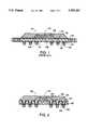
- FIG. 2is a cross-sectional view of a ball grid array 200 according to the invention.
- An integrated circuit chip 201is mounted on a substrate 202.
- the substrate 202may be a double-sided substrate (2-layer board) or multi-layer substrate.
- a plurality of bond pads(not shown) are formed on the integrated circuit chip 201. Selected ones of the bond pads are connected with electrically conductive bond wires 206 to electrically conductive traces 205 formed on the substrate 202.
- the integrated circuit chip 201can be connected using flip-chip interconnection or tape automated bonding (TAB).
- the traces 205extend to vias 207. Vias 207 are plated with electrically conductive material which makes electrical contact with traces 205. Electrically conductive pads 208 are formed at the bottom of vias 207 so that pads 208 are electrically connected to the plating in vias 207.
- Encapsulant 203encapsulates the integrated circuit chip 201 and fills in the vias 207.
- the encapsulant 203may be a molding resin or a potting resin.
- No vias 207are formed in substrate 202 outside of the encapsulant 203.
- Solder resistmay be applied between the substrate 202 and the encapsulant 203.
- solder balls 204are formed, as is well known, on pads 208. Solder balls 204 are then connected to, for instance, a printed circuit board by reflowing the solder balls 204 to form an attachment to electrically conductive material not part of the ball grid array, e.g., traces on the surface of the printed circuit board.
- integrated circuit chip 201is shown in FIG. 2, it is to be understood that additional integrated circuit chips, as well as passive components such as resistors or capacitors, can also be mounted on substrate 202.
- the vias 207can be formed by, for instance, mechanical drilling, laser drilling, etching or chemical milling. If the vias 207 are formed by laser drilling, either a thermal or non-thermal laser is used. If the substrate 202 is formed of organic material, a non-thermal laser, such as an excimer laser, is advantageously used.
- Vias 207can be formed in the substrate 202 by laser drilling as described in detail in applicants' co-pending U.S. patent application Ser. No. 07/893,518, entitled "Integrated Circuit Package with Via Interconnection Techniques and Method for Forming Such a Package.”
- a laser energy sourceemits laser energy that is focused by a lens into a sheet-shaped laser beam.
- the laser beamis passed over the surface of a mask positioned above the surface of the substrate 202.
- the masking technique usedcan be mask imaging, contact masking or conformal masking, each of which is discussed in greater detail in applicants' above-referenced co-pending U.S. patent application.
- Laser energypasses through holes formed in the mask at locations at which it is desired to form vias 207 in the substrate 202, cutting through the substrate 202 to the pads 208 formed on the bottom surface of the substrate 202.
- the laseris tuned to a frequency which ensures that the substrate 202 material in the to-be-formed via 207 is ablatively removed.
- the maskis of a material (such as copper) to which the laser is not tuned so that the mask is not ablatively affected by the laser.
- the laser energyis allowed to penetrate through the substrate 202, but prevented from penetrating through the pads 208 (which are formed of metal) by controlling the fluence of the laser.
- Fluencerepresents a combination of the duration of time for which the laser energy is applied and the intensity of the laser during the period of application. Since the metallic material of the pads 208 is much denser than the material of which the substrate 202 is formed, the fluence may be controlled so that the laser operates at a sufficiently great strength for a sufficiently long time to penetrate the substrate 202, but not the pads 208.
- the vias 207can be formed after the layers have been laminated together, as described above, or the vias 207 can be formed in advance in one or more layers of the substrate 202 and then laminating the layers together.
- FIG. 3is a cross-sectional view of a ball grid array 300 according to another embodiment of the invention.
- Integrated circuit chips 301a and 301bare attached to substrate 302.
- a plurality of bond pads(not shown) are formed on each of the integrated circuit chips 301a and 301b.
- Selected ones of the bond pads of the integrated circuit chip 301aare connected with electrically conductive bond wires 306 to electrically conductive traces 305 formed on the substrate 302.
- Electrically conductive bumps 311are formed on selected ones of the bond pads of the integrated circuit chip 301b.
- Each of the bumps 311is attached to an electrically conductive trace 305a formed on substrate 302 to form a conventional flip chip connection.
- the traces 305aextend to plated vias 307 which make electrical connection to between the traces 305a and electrically conductive pads 308 formed on the bottom surface of the substrate.
- Encapsulant 303encapsulates the integrated circuit chips 301a and 301b and fills in the vias 307. Solder balls 304 are formed on each of the pads 308.
- the substrate 302is a multilayer substrate. Conductive traces and/or regions formed on each layer are connected to conductive traces and/or regions formed on other layers by vias.
- the viasare formed by a laser, as described above.
- a sequential lamination techniquecan be used, in which one layer is stacked on another layer on which electrically conductive regions and/or traces have already been formed and in which vias have already been formed.
- a prepregis put on the substrate layers, and the layers are laminated using a vacuum press. The resin in the prepreg fills the vias as a result of resin flow during lamination.
- FIG. 4is a cross-sectional view of a ball grid array 400 according to another embodiment of the invention, including an integrated circuit chip 401, a substrate 402, encapsulant 403 and bond wires 406.
- Ball grid array 400is similar to ball grid array 100. Electrically conductive traces 405 are formed on a top surface of substrate 402. Plated vias 407 electrically connect traces 405 to pads 408 formed on the bottom surface of the substrate 402. Solder balls 404 are formed on each of the pads 408.
- a cavity 409is formed in substrate 402.
- Integrated circuit chip 401is attached in cavity 409 with a conventional die attach adhesive 412.
- a conventional die attach adhesive 412.Such an arrangement may be desirable as a means to supply ground and power plane voltages, provide heat dissipation from the chip, decrease the package profile, allow tighter grouping of integrated circuit chips and other components, or reduce the signal transmission length from the integrated circuit.
- the chipmay be formed with a conductive underside that is electrically connected to a conductive cavity floor.
- the cavity 409can be formed with a laser using the methods described above.
- the maskis patterned with larger openings than used to form vias 407.
- the use of a laseris preferable to accomplish this cavity formation because the laser overcomes the tolerance problems (e.g., cavity depth, corner radius, X-Y tolerance, damage to adjacent areas) associated with the previously used mechanical milling approach.
- small vias 413are formed through substrate 402 within cavity 409.
- the vias 413are filled with, for instance, an epoxy resin. The presence of the vias 413 improves heat transfer from the chip 401 to the exterior of the ball grid array 400.
- FIG. 5is a cross-sectional view of a ball grid array 500 according to another embodiment of the invention.
- a hole 509is formed completely through the substrate 502 in a location corresponding to the location of the cavity 409 of ball grid array 400 (FIG. 4).
- a cavity 513is formed adjacent hole 509 to create a surface 502c of substrate 502 that is recessed relative to surface 502b.
- the hole 509 and cavity 513can be formed using the previously described laser techniques.
- An integrated circuit chip 501is attached to a heat sink 510 with a conventional adhesive 512.
- the heat sink 510can be formed of any material having an acceptably high thermal conductivity such as copper.
- the heat sink 510is attached to a surface 502a of substrate 502 with an adhesive 511, such as an epoxy adhesive, such that integrated circuit chip 501 extends through the hole 509. Bond pads (not shown) on the integrated circuit chip 501 are connected with bond wires 506 to electrically conductive traces 514 formed on surface 502c. Electrically conductive traces 505 are also formed on an interior layer of substrate 502. Plated vias 507 electrically connect traces 505 and 514 to each other and to electrically conductive pads 508. Solder balls 504 are formed on pads 508. Encapsulant 503 is filled into hole 509 and cavity 513 to encapsulate the integrated circuit chip 501.
- an adhesive 511such as an epoxy adhesive
- the presence of the heat sink 510 in ball grid array 500provides good heat transfer away from the chip 501, particularly since most of the heat sink surface is exposed to the exterior of the ball grid array 500.
- FIG. 6is a cross-sectional view of a ball grid array 600 according to another embodiment of the invention.
- Plated vias 607are formed through the substrate 602. Except for vias 607 near the edge of the substrate 602, vias 607 are filled with an epoxy resin 609. However, this need not be the case, and all vias 607 can be filled with epoxy resin 609.
- the integrated circuit chip 601is attached to the substrate 602 with an adhesive 612 such that the chip 601 covers some of the vias 607. Bond pads (not shown) on the chip 601 are electrically connected with bond wires 606 to electrically conductive traces 605 on the substrate 602.
- the vias 607electrically connect the traces 605 to electrically conductive pads 608 on which solder balls 604 are formed.
- An encapsulant 603is formed over the chip 601 and bond wires 606 by potting.
- organic materialse.g., thermosetting or thermoplastic resins
- organic fiber reinforcemente.g., aramid fibers
- organic substratesare less expensive than inorganic substrates (e.g., glass or ceramic).
- organic materialsmay be penetrated with a laser more easily and quickly than inorganic materials.
- organic materialshave better dielectric properties than inorganic materials.
- the use of a thermal laserproduces undesirable side effects such as dielectric degradation, charring and surface reflow. Because of these problems, it has been necessary either to use the more expensive ceramic or glass organic substrates if use of a thermal laser is contemplated, or perform mechanical drilling to form the vias in an organic substrate.
- the substrate layer or layersare formed of organic material.
- Viasare formed in the substrate using a non-thermal laser (e.g., an excimer laser), thus avoiding the detrimental effects associated with the use of thermal lasers or mechanical drills.
- a non-thermal lasere.g., an excimer laser
- thermosetting resinsare preferably chosen from the following group: epoxy, polyimide, polyamide, polyetherimide or polycyanurate.
- the thermoplastic resinsare preferably chosen from the following group: polyester, polyamide, polysulfone, polyetherimide, polycarbonate.
- Epoxy resinis most desirable because of its low cost, its ready availability and wide knowledge of its properties.
- an epoxy resin having high temperature resistanceis used so that high hole quality is maintained.
- Epoxy resin with low ionic contenti.e., low impurity levels
- Organic fiber reinforcementmay also be used in the organic resin.
- Fibers that may be usedinclude: aramid, polyester, polyamide, poly-ether-ether-ketone, polyimide, polyetherimide, or polysulfone.
- the fibersmay include inorganic fillers such as, alumina or silica, as long as the fillers do not impede penetration by the laser.
- aramid fibersare used, such as poly-(paraphenylene terephthalamide) and co-poly-(paraphenylene/3,4'-diphenylether terephthalamide), since these fibers are easily fabricated into substrates. In particular, the latter fiber has higher purity in terms of ionic content.
- the fiber reinforcementcan be woven fabric, non-woven fabric or paper. Paper reinforcements may be preferable due to their flat surface which allows easy mounting of integrated circuit chips or passive components.
- the region of the top surface of the substrate outside of the area in which the integrated circuit chip is to be attachedis patterned and etched to form a conductive interconnection pattern. This may be done either before or after the substrate is constructed as described above. If the conformal mask technique is used, the mask may be left in place after formation of the vias, and the interconnection pattern is formed on the exposed surface of the mask. Interconnection of the conductive interconnection pattern to individual integrated circuit chips and passive components can be done by wirebonding, TAB, flip-chip, or other bonding technologies.
- the chips and passive componentsare then encapsulated with a molding or potting resin such as epoxy, polyimide or poly-bismaleimide resin, to protect the integrated circuit chip or chips and the passive components.
- a molding or potting resinsuch as epoxy, polyimide or poly-bismaleimide resin
- a resin containing an aramid fiber formed of co-poly-(paraphenylene/3,4'-diphenylether terephthalamide), having a diameter of 12 microns and a length of 3 mmis sheet-formed using a paper machine.
- the resincontains 15% organic binder from water-soluble epoxy.
- the basis weight of the paperis 72 g/m 2 .
- the paperis impregnated with an epoxy resin including a hardener or a Novolac type resin to form a prepreg.
- the fiber content of the prepregis 45% by weight.
- the prepregis laminated to form a sheet having a thickness of 0.1 mm. Details of the preparation are described in Japanese Open Patent 1-281791.
- Copper foils having a thickness of 18 micronsare laminated to both sides of the prepreg using an epoxy adhesive.
- the total thickness of the insulation layer (including the epoxy adhesive layer)is typically 0.08-0.15 mm.
- One side of the copperis etched to form holes, and vias are formed with a Kr/F excimer laser using a conformal masking method.
- the laserhas a wavelength of 248 nm.
- the frequency of the laser beamis 200 Hz and the pulse energy is 1.6 J/cm 2 .
- the holesare subjected to an ablation of 7 seconds.
- the viasare then plated with copper to electrically connect the copper foils.
- Both sides of copperare pattern-etched to form a substrate. In pattern-etching, the bottom of the vias form round pads.
- the number of tracesis 225.
- An integrated circuit chipis adhesively attached to the top of the substrate, and wire-bonded to pads on the top of the substrate which are connected to pads on the bottom of the substrate.
- a molding resinis molded on the top of the substrate to encapsulate the semiconductive chips and traces. Solder balls are attached to the pads on the bottom of the substrate, and reflow attached at 230° C.
- the completed ball grid arrayis mounted on a printed circuit board, and reflow attached at 230° C.
- the same laminate as in the first exampleis formed.
- One side of the laminateis patterned for laser drilling, and laser ablation is applied.
- pattern-etchingis made to form a "core" substrate.
- a sheet of prepregis then stacked and press-cured together with a copper foil on the top.
- the top copperis then etched, and the top layer is laser-ablated, plated and pattern-etched.
- the second layeris also fabricated.
Landscapes
- Engineering & Computer Science (AREA)
- Microelectronics & Electronic Packaging (AREA)
- Physics & Mathematics (AREA)
- Condensed Matter Physics & Semiconductors (AREA)
- General Physics & Mathematics (AREA)
- Computer Hardware Design (AREA)
- Power Engineering (AREA)
- Production Of Multi-Layered Print Wiring Board (AREA)
Abstract
Description
Claims (17)
Priority Applications (2)
| Application Number | Priority Date | Filing Date | Title |
|---|---|---|---|
| US08/047,721US5355283A (en) | 1993-04-14 | 1993-04-14 | Ball grid array with via interconnection |
| JP06101854AJP3111134B2 (en) | 1993-04-14 | 1994-04-14 | Packaged integrated circuit and method of forming the same |
Applications Claiming Priority (1)
| Application Number | Priority Date | Filing Date | Title |
|---|---|---|---|
| US08/047,721US5355283A (en) | 1993-04-14 | 1993-04-14 | Ball grid array with via interconnection |
Publications (1)
| Publication Number | Publication Date |
|---|---|
| US5355283Atrue US5355283A (en) | 1994-10-11 |
Family
ID=21950553
Family Applications (1)
| Application Number | Title | Priority Date | Filing Date |
|---|---|---|---|
| US08/047,721Expired - LifetimeUS5355283A (en) | 1993-04-14 | 1993-04-14 | Ball grid array with via interconnection |
Country Status (2)
| Country | Link |
|---|---|
| US (1) | US5355283A (en) |
| JP (1) | JP3111134B2 (en) |
Cited By (306)
| Publication number | Priority date | Publication date | Assignee | Title |
|---|---|---|---|---|
| US5454159A (en)* | 1994-02-18 | 1995-10-03 | Unisys Corporation | Method of manufacturing I/O terminals on I/O pads |
| US5459287A (en)* | 1994-05-18 | 1995-10-17 | Dell Usa, L.P. | Socketed printed circuit board BGA connection apparatus and associated methods |
| US5467253A (en)* | 1994-06-30 | 1995-11-14 | Motorola, Inc. | Semiconductor chip package and method of forming |
| WO1996012298A1 (en)* | 1993-08-05 | 1996-04-25 | Vlsi Technology, Inc. | Thin cavity down ball grid array package based on wirebond technology |
| US5525834A (en)* | 1994-10-17 | 1996-06-11 | W. L. Gore & Associates, Inc. | Integrated circuit package |
| US5541450A (en)* | 1994-11-02 | 1996-07-30 | Motorola, Inc. | Low-profile ball-grid array semiconductor package |
| WO1996027280A1 (en)* | 1995-03-02 | 1996-09-06 | Intel Corporation | Thermally and electrically enhanced ball grid package |
| US5557150A (en)* | 1992-02-07 | 1996-09-17 | Lsi Logic Corporation | Overmolded semiconductor package |
| US5563446A (en)* | 1994-01-25 | 1996-10-08 | Lsi Logic Corporation | Surface mount peripheral leaded and ball grid array package |
| US5572405A (en)* | 1995-06-07 | 1996-11-05 | International Business Machines Corporation (Ibm) | Thermally enhanced ball grid array package |
| WO1996025763A3 (en)* | 1995-02-15 | 1996-11-07 | Ibm | Organic chip carriers for wire bond-type chips |
| GB2301937A (en)* | 1995-06-06 | 1996-12-18 | Circuit Components Inc | IC package with a ball grid array on a single layer ceramic substrate |
| US5587885A (en)* | 1994-05-18 | 1996-12-24 | Dell Usa, L.P. | Mechanical printed circuit board/laminated multi chip module interconnect apparatus |
| US5609889A (en)* | 1995-05-26 | 1997-03-11 | Hestia Technologies, Inc. | Apparatus for encapsulating electronic packages |
| EP0675539A3 (en)* | 1994-03-30 | 1997-05-21 | Plessey Semiconductors Ltd | Ball grid housing with integrated passive circuit elements. |
| US5636104A (en)* | 1995-05-31 | 1997-06-03 | Samsung Electronics Co., Ltd. | Printed circuit board having solder ball mounting groove pads and a ball grid array package using such a board |
| US5640048A (en)* | 1994-07-11 | 1997-06-17 | Sun Microsystems, Inc. | Ball grid array package for a integrated circuit |
| US5639696A (en)* | 1996-01-31 | 1997-06-17 | Lsi Logic Corporation | Microelectronic integrated circuit mounted on circuit board with solder column grid array interconnection, and method of fabricating the solder column grid array |
| WO1997023123A1 (en)* | 1995-12-20 | 1997-06-26 | Intel Corporation | A ball grid array integrated circuit package that has vias located within the solder pads |
| US5646828A (en)* | 1995-02-24 | 1997-07-08 | Lucent Technologies Inc. | Thin packaging of multi-chip modules with enhanced thermal/power management |
| US5650593A (en)* | 1994-05-26 | 1997-07-22 | Amkor Electronics, Inc. | Thermally enhanced chip carrier package |
| US5652463A (en)* | 1995-05-26 | 1997-07-29 | Hestia Technologies, Inc. | Transfer modlded electronic package having a passage means |
| US5656550A (en)* | 1994-08-24 | 1997-08-12 | Fujitsu Limited | Method of producing a semicondutor device having a lead portion with outer connecting terminal |
| US5659952A (en)* | 1994-09-20 | 1997-08-26 | Tessera, Inc. | Method of fabricating compliant interface for semiconductor chip |
| US5661088A (en)* | 1996-01-11 | 1997-08-26 | Motorola, Inc. | Electronic component and method of packaging |
| WO1997036466A1 (en)* | 1996-03-28 | 1997-10-02 | Intel Corporation | Perimeter matrix ball grid array circuit package with a populated center |
| WO1997037383A1 (en)* | 1996-04-02 | 1997-10-09 | Micron Technology, Inc. | Standardized bonding location process and apparatus |
| US5677566A (en)* | 1995-05-08 | 1997-10-14 | Micron Technology, Inc. | Semiconductor chip package |
| US5696031A (en)* | 1996-11-20 | 1997-12-09 | Micron Technology, Inc. | Device and method for stacking wire-bonded integrated circuit dice on flip-chip bonded integrated circuit dice |
| US5701032A (en)* | 1994-10-17 | 1997-12-23 | W. L. Gore & Associates, Inc. | Integrated circuit package |
| US5706174A (en)* | 1994-07-07 | 1998-01-06 | Tessera, Inc. | Compliant microelectrionic mounting device |
| US5708300A (en)* | 1995-09-05 | 1998-01-13 | Woosley; Alan H. | Semiconductor device having contoured package body profile |
| US5714803A (en)* | 1995-07-28 | 1998-02-03 | Sgs-Thomson Microelectronics, Inc. | Low-profile removable ball-grid-array integrated circuit package |
| US5729050A (en)* | 1996-03-11 | 1998-03-17 | Lg Semicon Co., Ltd. | Semiconductor package substrate and ball grid array (BGA) semiconductor package using same |
| US5731709A (en)* | 1996-01-26 | 1998-03-24 | Motorola, Inc. | Method for testing a ball grid array semiconductor device and a device for such testing |
| US5734106A (en)* | 1993-09-30 | 1998-03-31 | Commissariat A L 'energie Atomique | Integrated electronic sensor for characterizing physical quantities and process for producing such a sensor |
| US5736789A (en)* | 1994-07-26 | 1998-04-07 | Sgs-Thomson Microelectronics S.A. | Ball grid array casing for integrated circuits |
| US5766021A (en)* | 1996-10-01 | 1998-06-16 | Augat Inc. | BGA interconnectors |
| US5776796A (en)* | 1994-05-19 | 1998-07-07 | Tessera, Inc. | Method of encapsulating a semiconductor package |
| US5784260A (en)* | 1996-05-29 | 1998-07-21 | International Business Machines Corporation | Structure for constraining the flow of encapsulant applied to an I/C chip on a substrate |
| EP0853817A1 (en)* | 1995-10-04 | 1998-07-22 | International Business Machines Corporation | Electronic package with enhanced pad design |
| US5786238A (en)* | 1997-02-13 | 1998-07-28 | Generyal Dynamics Information Systems, Inc. | Laminated multilayer substrates |
| US5789813A (en)* | 1996-09-30 | 1998-08-04 | Lsi Logic Corporation | Ball grid array package with inexpensive threaded secure locking mechanism to allow removal of a threaded heat sink therefrom |
| US5815372A (en)* | 1997-03-25 | 1998-09-29 | Intel Corporation | Packaging multiple dies on a ball grid array substrate |
| US5825628A (en)* | 1996-10-03 | 1998-10-20 | International Business Machines Corporation | Electronic package with enhanced pad design |
| US5827999A (en)* | 1994-05-26 | 1998-10-27 | Amkor Electronics, Inc. | Homogeneous chip carrier package |
| GB2324649A (en)* | 1997-04-16 | 1998-10-28 | Ibm | Shielded semiconductor package |
| US5831832A (en)* | 1997-08-11 | 1998-11-03 | Motorola, Inc. | Molded plastic ball grid array package |
| US5833472A (en)* | 1995-07-27 | 1998-11-10 | The Whitaker Corporation | Socket assembly for an electronic package |
| US5832600A (en)* | 1995-06-06 | 1998-11-10 | Seiko Epson Corporation | Method of mounting electronic parts |
| WO1998053499A1 (en) | 1997-05-20 | 1998-11-26 | Micro Components Ltd. | Substrate for electronic packaging, pin jig fixture |
| US5849609A (en)* | 1995-03-28 | 1998-12-15 | Lg Semicon Co., Ltd. | Semiconductor package and a method of manufacturing thereof |
| US5852870A (en)* | 1996-04-24 | 1998-12-29 | Amkor Technology, Inc. | Method of making grid array assembly |
| US5859475A (en)* | 1996-04-24 | 1999-01-12 | Amkor Technology, Inc. | Carrier strip and molded flex circuit ball grid array |
| US5859474A (en)* | 1997-04-23 | 1999-01-12 | Lsi Logic Corporation | Reflow ball grid array assembly |
| US5892290A (en)* | 1995-10-28 | 1999-04-06 | Institute Of Microelectronics | Highly reliable and planar ball grid array package |
| US5893724A (en)* | 1995-10-28 | 1999-04-13 | Institute Of Microelectronics | Method for forming a highly reliable and planar ball grid array package |
| US5909054A (en)* | 1995-05-16 | 1999-06-01 | Kabushiki Kaisha Toshiba | Semiconductor device having a multiple-terminal integrated circuit formed on a circuit substrate |
| US5915170A (en)* | 1994-09-20 | 1999-06-22 | Tessera, Inc. | Multiple part compliant interface for packaging of a semiconductor chip and method therefor |
| KR19990045687A (en)* | 1997-11-28 | 1999-06-25 | 이데이 노부유끼 | Semiconductor device, manufacturing method thereof and electronic device using same |
| US5918153A (en)* | 1996-09-18 | 1999-06-29 | Sandia Corporation | High density electronic circuit and process for making |
| US5920117A (en)* | 1994-08-02 | 1999-07-06 | Fujitsu Limited | Semiconductor device and method of forming the device |
| US5923959A (en)* | 1997-07-23 | 1999-07-13 | Micron Technology, Inc. | Ball grid array (BGA) encapsulation mold |
| US5923954A (en)* | 1997-03-14 | 1999-07-13 | Lg Semicon Co., Ltd. | Ball grid array package and fabrication method therefor |
| US5950072A (en)* | 1997-07-25 | 1999-09-07 | Stmicroelectronics, Inc. | Low-profile removable ball-grid-array integrated circuit package |
| US5969426A (en)* | 1994-12-14 | 1999-10-19 | Mitsubishi Denki Kabushiki Kaisha | Substrateless resin encapsulated semiconductor device |
| US5966803A (en)* | 1996-05-31 | 1999-10-19 | International Business Machines Corporation | Ball grid array having no through holes or via interconnections |
| US5972734A (en)* | 1997-09-17 | 1999-10-26 | Lsi Logic Corporation | Interposer for ball grid array (BGA) package |
| US5982633A (en)* | 1997-08-20 | 1999-11-09 | Compaq Computer Corporation | Opposed ball grid array mounting |
| WO1999057762A1 (en)* | 1998-05-02 | 1999-11-11 | Eriston Investment Pte Ltd. | Flip chip assembly with via interconnection |
| US5989935A (en)* | 1996-11-19 | 1999-11-23 | Texas Instruments Incorporated | Column grid array for semiconductor packaging and method |
| US5989937A (en)* | 1994-02-04 | 1999-11-23 | Lsi Logic Corporation | Method for compensating for bottom warpage of a BGA integrated circuit |
| EP0905521A3 (en)* | 1997-09-26 | 1999-12-01 | Molex Incorporated | Burn-in testing device |
| US6008538A (en)* | 1996-10-08 | 1999-12-28 | Micron Technology, Inc. | Method and apparatus providing redundancy for fabricating highly reliable memory modules |
| US6015955A (en)* | 1997-06-20 | 2000-01-18 | International Business Machines Corporation | Reworkability solution for wirebound chips using high performance capacitor |
| US6025650A (en)* | 1994-08-24 | 2000-02-15 | Fujitsu Limited | Semiconductor device including a frame terminal |
| US6024584A (en)* | 1996-10-10 | 2000-02-15 | Berg Technology, Inc. | High density connector |
| US6031284A (en)* | 1997-03-14 | 2000-02-29 | Lg Semicon Co., Ltd. | Package body and semiconductor chip package using same |
| JP3024506B2 (en) | 1995-02-28 | 2000-03-21 | 住友金属工業株式会社 | Connection method between Si chip and package |
| US6039889A (en)* | 1999-01-12 | 2000-03-21 | Fujitsu Limited | Process flows for formation of fine structure layer pairs on flexible films |
| US6042389A (en)* | 1996-10-10 | 2000-03-28 | Berg Technology, Inc. | Low profile connector |
| US6051890A (en)* | 1997-12-24 | 2000-04-18 | Intel Corporation | Interleaving a bondwire between two bondwires coupled to a same terminal |
| US6052287A (en)* | 1997-12-09 | 2000-04-18 | Sandia Corporation | Silicon ball grid array chip carrier |
| US6054338A (en)* | 1996-05-17 | 2000-04-25 | National Semiconductor Corporation | Low cost ball grid array device and method of manufacture thereof |
| US6057595A (en)* | 1996-06-28 | 2000-05-02 | Siemens Aktiengesellschaft | Integrated semiconductor circuit housing |
| US6074894A (en)* | 1996-09-02 | 2000-06-13 | Matsushita Electric Industrial Co., Ltd. | Mounting method of semiconductor device |
| US6093035A (en)* | 1996-06-28 | 2000-07-25 | Berg Technology, Inc. | Contact for use in an electrical connector |
| US6114189A (en)* | 1997-09-10 | 2000-09-05 | Lsi Logic Corp. | Molded array integrated circuit package |
| US6120885A (en)* | 1997-07-10 | 2000-09-19 | International Business Machines Corporation | Structure, materials, and methods for socketable ball grid |
| US6125042A (en)* | 1998-04-10 | 2000-09-26 | Lucent Technologies, Inc. | Ball grid array semiconductor package having improved EMI characteristics |
| US6137163A (en)* | 1997-09-12 | 2000-10-24 | Hyundai Electronics Industries Co., Ltd. | Semiconductor substrate and stackable semiconductor package and fabrication method thereof |
| US6139336A (en)* | 1996-11-14 | 2000-10-31 | Berg Technology, Inc. | High density connector having a ball type of contact surface |
| US6140708A (en)* | 1996-05-17 | 2000-10-31 | National Semiconductor Corporation | Chip scale package and method for manufacture thereof |
| US6140707A (en)* | 1998-05-07 | 2000-10-31 | 3M Innovative Properties Co. | Laminated integrated circuit package |
| US6146203A (en)* | 1995-06-12 | 2000-11-14 | Berg Technology, Inc. | Low cross talk and impedance controlled electrical connector |
| US6154372A (en)* | 1993-09-02 | 2000-11-28 | Siemens Aktiengesellschaft | Multichip module for surface mounting on printed circuit boards |
| US6163069A (en)* | 1997-10-09 | 2000-12-19 | Mitsubishi Denki Kabushiki Kaisha | Semiconductor device having pads for connecting a semiconducting element to a mother board |
| US6169328B1 (en) | 1994-09-20 | 2001-01-02 | Tessera, Inc | Semiconductor chip assembly |
| US6187652B1 (en)* | 1998-09-14 | 2001-02-13 | Fujitsu Limited | Method of fabrication of multiple-layer high density substrate |
| US6191494B1 (en)* | 1998-06-30 | 2001-02-20 | Fujitsu Limited | Semiconductor device and method of producing the same |
| US6214640B1 (en) | 1999-02-10 | 2001-04-10 | Tessera, Inc. | Method of manufacturing a plurality of semiconductor packages |
| GB2356490A (en)* | 1996-08-27 | 2001-05-23 | Nec Corp | A multi-chip module mounted on a printed circuit board |
| US6241535B1 (en) | 1996-10-10 | 2001-06-05 | Berg Technology, Inc. | Low profile connector |
| US20010002624A1 (en)* | 1993-11-16 | 2001-06-07 | Igor Y. Khandros | Tip structures. |
| US6247229B1 (en)* | 1999-08-25 | 2001-06-19 | Ankor Technology, Inc. | Method of forming an integrated circuit device package using a plastic tape as a base |
| US6255143B1 (en) | 1999-08-04 | 2001-07-03 | St. Assembly Test Services Pte Ltd. | Flip chip thermally enhanced ball grid array |
| US6281096B1 (en) | 1999-04-22 | 2001-08-28 | International Rectifier Corp. | Chip scale packaging process |
| US6284566B1 (en) | 1996-05-17 | 2001-09-04 | National Semiconductor Corporation | Chip scale package and method for manufacture thereof |
| US6286208B1 (en)* | 1995-09-13 | 2001-09-11 | International Business Machines Corporation | Interconnector with contact pads having enhanced durability |
| US6297559B1 (en) | 1997-07-10 | 2001-10-02 | International Business Machines Corporation | Structure, materials, and applications of ball grid array interconnections |
| US6316837B1 (en) | 1997-12-04 | 2001-11-13 | Hyundai Electronics Industries Co., Ltd. | Area array type semiconductor package and fabrication method |
| US6316830B1 (en) | 1998-12-17 | 2001-11-13 | Charles Wen Chyang Lin | Bumpless flip chip assembly with strips and via-fill |
| US6324069B1 (en)* | 1997-10-29 | 2001-11-27 | Hestia Technologies, Inc. | Chip package with molded underfill |
| US6325644B1 (en) | 1996-10-10 | 2001-12-04 | Berg Technology, Inc. | High density connector and method of manufacture |
| US6329713B1 (en) | 1998-10-21 | 2001-12-11 | International Business Machines Corporation | Integrated circuit chip carrier assembly comprising a stiffener attached to a dielectric substrate |
| US6329702B1 (en) | 2000-07-06 | 2001-12-11 | Tyco Electronics Corporation | High frequency carrier |
| US6329711B1 (en)* | 1995-11-08 | 2001-12-11 | Fujitsu Limited | Semiconductor device and mounting structure |
| US6337522B1 (en) | 1997-07-10 | 2002-01-08 | International Business Machines Corporation | Structure employing electrically conductive adhesives |
| US20020014346A1 (en)* | 2000-06-14 | 2002-02-07 | Nec Corporation | Mounting structure of semiconductor package |
| US6348728B1 (en)* | 2000-01-28 | 2002-02-19 | Fujitsu Limited | Semiconductor device having a plurality of semiconductor elements interconnected by a redistribution layer |
| US6350633B1 (en) | 2000-08-22 | 2002-02-26 | Charles W. C. Lin | Semiconductor chip assembly with simultaneously electroplated contact terminal and connection joint |
| US6350386B1 (en)* | 2000-09-20 | 2002-02-26 | Charles W. C. Lin | Method of making a support circuit with a tapered through-hole for a semiconductor chip assembly |
| US6350632B1 (en) | 2000-09-20 | 2002-02-26 | Charles W. C. Lin | Semiconductor chip assembly with ball bond connection joint |
| US6365980B1 (en)* | 1999-02-26 | 2002-04-02 | Texas Instruments Incorporated | Thermally enhanced semiconductor ball grid array device and method of fabrication |
| US6372540B1 (en) | 2000-04-27 | 2002-04-16 | Amkor Technology, Inc. | Moisture-resistant integrated circuit chip package and method |
| US20020045290A1 (en)* | 1996-02-20 | 2002-04-18 | Michael B. Ball | Flip chip and conventional stack |
| US6376921B1 (en)* | 1995-11-08 | 2002-04-23 | Fujitsu Limited | Semiconductor device, method for fabricating the semiconductor device, lead frame and method for producing the lead frame |
| US20020053452A1 (en)* | 1996-09-04 | 2002-05-09 | Quan Son Ky | Semiconductor package and method therefor |
| US6395992B1 (en) | 1998-12-01 | 2002-05-28 | Nhk Spring Co., Ltd. | Three-dimensional wiring board and electric insulating member for wiring board |
| US20020064907A1 (en)* | 1999-06-18 | 2002-05-30 | Brand Joseph M. | Method of fabricating an encapsulant lock feature in integrated circuit packaging |
| US6403400B2 (en) | 1998-12-17 | 2002-06-11 | Charles Wen Chyang Lin | Bumpless flip chip assembly with strips-in-via and plating |
| US6403460B1 (en) | 2000-08-22 | 2002-06-11 | Charles W. C. Lin | Method of making a semiconductor chip assembly |
| US6402970B1 (en) | 2000-08-22 | 2002-06-11 | Charles W. C. Lin | Method of making a support circuit for a semiconductor chip assembly |
| US6407458B1 (en)* | 2000-05-04 | 2002-06-18 | Amkor Technology, Inc. | Moisture-resistant integrated circuit chip package and method |
| US6406939B1 (en) | 1998-05-02 | 2002-06-18 | Charles W. C. Lin | Flip chip assembly with via interconnection |
| US6410979B2 (en)* | 1998-12-21 | 2002-06-25 | Nec Corporation | Ball-grid-array semiconductor device with protruding terminals |
| US20020094606A1 (en)* | 1994-03-18 | 2002-07-18 | Hitachi Chemical Company, Ltd. | Fabrication process of semiconductor package and semiconductor package |
| US6429513B1 (en) | 2001-05-25 | 2002-08-06 | Amkor Technology, Inc. | Active heat sink for cooling a semiconductor chip |
| US6436734B1 (en) | 2000-08-22 | 2002-08-20 | Charles W. C. Lin | Method of making a support circuit for a semiconductor chip assembly |
| US6440770B1 (en) | 1996-09-09 | 2002-08-27 | Intel Corporation | Integrated circuit package |
| US6441498B1 (en) | 1997-12-02 | 2002-08-27 | Hyundai Electronics Industries Co., Ltd. | Semiconductor substrate and land grid array semiconductor package using same |
| US6440835B1 (en) | 2000-10-13 | 2002-08-27 | Charles W. C. Lin | Method of connecting a conductive trace to a semiconductor chip |
| US6444489B1 (en) | 2000-12-15 | 2002-09-03 | Charles W. C. Lin | Semiconductor chip assembly with bumped molded substrate |
| US6448108B1 (en) | 2000-10-02 | 2002-09-10 | Charles W. C. Lin | Method of making a semiconductor chip assembly with a conductive trace subtractively formed before and after chip attachment |
| US6455354B1 (en) | 1998-12-30 | 2002-09-24 | Micron Technology, Inc. | Method of fabricating tape attachment chip-on-board assemblies |
| US20020140085A1 (en)* | 2001-04-02 | 2002-10-03 | Lee Sang Ho | Semiconductor package including passive elements and method of manufacture |
| US6465743B1 (en)* | 1994-12-05 | 2002-10-15 | Motorola, Inc. | Multi-strand substrate for ball-grid array assemblies and method |
| US6472252B2 (en) | 1997-07-23 | 2002-10-29 | Micron Technology, Inc. | Methods for ball grid array (BGA) encapsulation mold |
| US20020158335A1 (en)* | 2001-04-30 | 2002-10-31 | Intel Corporation | High performance, low cost microelectronic circuit package with interposer |
| US6476331B1 (en) | 2000-06-19 | 2002-11-05 | Amkor Technology, Inc. | Printed circuit board for semiconductor package and method for manufacturing the same |
| US6476472B1 (en) | 2000-08-18 | 2002-11-05 | Agere Systems Inc. | Integrated circuit package with improved ESD protection for no-connect pins |
| DE10120257A1 (en)* | 2001-04-25 | 2002-11-14 | Siemens Production & Logistics | Connection carrier for an electronic component and method for its production |
| US20020167804A1 (en)* | 2001-05-14 | 2002-11-14 | Intel Corporation | Polymeric encapsulation material with fibrous filler for use in microelectronic circuit packaging |
| US6492252B1 (en) | 2000-10-13 | 2002-12-10 | Bridge Semiconductor Corporation | Method of connecting a bumped conductive trace to a semiconductor chip |
| US6495083B2 (en) | 1997-10-29 | 2002-12-17 | Hestia Technologies, Inc. | Method of underfilling an integrated circuit chip |
| US6507122B2 (en)* | 1999-08-09 | 2003-01-14 | International Business Machines Corporation | Pre-bond encapsulation of area array terminated chip and wafer scale packages |
| US6511865B1 (en) | 2000-09-20 | 2003-01-28 | Charles W. C. Lin | Method for forming a ball bond connection joint on a conductive trace and conductive pad in a semiconductor chip assembly |
| US20030025190A1 (en)* | 2001-08-06 | 2003-02-06 | Byun Hyung Jik | Tape ball grid array semiconductor chip package having ball land pad isolated from adhesive, a method of manufacturing the same and a multi-chip package |
| EP1284502A1 (en)* | 1995-11-08 | 2003-02-19 | Fujitsu Limited | Device having resin package and method of producing the same |
| US6528891B2 (en) | 1998-12-17 | 2003-03-04 | Charles Wen Chyang Lin | Bumpless flip chip assembly with solder via |
| US20030052420A1 (en)* | 2001-09-18 | 2003-03-20 | Hitachi, Ltd. | Semiconductor device |
| US6537851B1 (en) | 2000-10-13 | 2003-03-25 | Bridge Semiconductor Corporation | Method of connecting a bumped compliant conductive trace to a semiconductor chip |
| US6544813B1 (en) | 2000-10-02 | 2003-04-08 | Charles W. C. Lin | Method of making a semiconductor chip assembly with a conductive trace subtractively formed before and after chip attachment |
| US6548393B1 (en) | 2000-10-13 | 2003-04-15 | Charles W. C. Lin | Semiconductor chip assembly with hardened connection joint |
| US6551861B1 (en) | 2000-08-22 | 2003-04-22 | Charles W. C. Lin | Method of making a semiconductor chip assembly by joining the chip to a support circuit with an adhesive |
| US6551112B1 (en) | 2002-03-18 | 2003-04-22 | High Connection Density, Inc. | Test and burn-in connector |
| US6562657B1 (en) | 2000-08-22 | 2003-05-13 | Charles W. C. Lin | Semiconductor chip assembly with simultaneously electrolessly plated contact terminal and connection joint |
| US6562709B1 (en) | 2000-08-22 | 2003-05-13 | Charles W. C. Lin | Semiconductor chip assembly with simultaneously electroplated contact terminal and connection joint |
| US20030089524A1 (en)* | 1999-01-27 | 2003-05-15 | Ngk Spark Plug Co., Ltd. | Resin substrate |
| US6576539B1 (en) | 2000-10-13 | 2003-06-10 | Charles W.C. Lin | Semiconductor chip assembly with interlocked conductive trace |
| US6576493B1 (en) | 2000-10-13 | 2003-06-10 | Bridge Semiconductor Corporation | Method of connecting a conductive trace and an insulative base to a semiconductor chip using multiple etch steps |
| US6583040B1 (en) | 2000-10-13 | 2003-06-24 | Bridge Semiconductor Corporation | Method of making a pillar in a laminated structure for a semiconductor chip assembly |
| US6586677B2 (en) | 1999-08-25 | 2003-07-01 | Amkor Technology, Inc. | Plastic integrated circuit device package having exposed lead surface |
| US6614660B1 (en) | 2002-04-30 | 2003-09-02 | Ultratera Corporation | Thermally enhanced IC chip package |
| US20030165052A1 (en)* | 2002-03-01 | 2003-09-04 | Mikio Negishi | Semiconductor device and manufacturing the same |
| US6617525B2 (en)* | 1999-02-12 | 2003-09-09 | St. Assembly Test Services Ltd. | Molded stiffener for flexible circuit molding |
| US6627823B1 (en)* | 1998-12-08 | 2003-09-30 | Alexander Ivanovich Taran | Multilayered connection plate |
| US20030186486A1 (en)* | 2002-03-28 | 2003-10-02 | Swan Johanna M. | Integrated circuit die and an electronic assembly having a three-dimensional interconnection scheme |
| US20030183943A1 (en)* | 2002-03-28 | 2003-10-02 | Swan Johanna M. | Integrated circuit die and an electronic assembly having a three-dimensional interconnection scheme |
| DE19627663C2 (en)* | 1995-07-28 | 2003-10-02 | Agilent Technologies Inc | Hybrid printed circuit board |
| US6630629B2 (en)* | 2000-01-27 | 2003-10-07 | Sanyo Electric Co., Ltd. | Wiring substrate |
| US6642624B2 (en)* | 1999-05-31 | 2003-11-04 | Nec Corporation | Ball grid array type semiconductor device |
| US6653170B1 (en) | 2001-02-06 | 2003-11-25 | Charles W. C. Lin | Semiconductor chip assembly with elongated wire ball bonded to chip and electrolessly plated to support circuit |
| US6653740B2 (en) | 2000-02-10 | 2003-11-25 | International Rectifier Corporation | Vertical conduction flip-chip device with bump contacts on single surface |
| US6660559B1 (en) | 2001-06-25 | 2003-12-09 | Amkor Technology, Inc. | Method of making a chip carrier package using laser ablation |
| US6660626B1 (en) | 2000-08-22 | 2003-12-09 | Charles W. C. Lin | Semiconductor chip assembly with simultaneously electrolessly plated contact terminal and connection joint |
| US6667229B1 (en) | 2000-10-13 | 2003-12-23 | Bridge Semiconductor Corporation | Method of connecting a bumped compliant conductive trace and an insulative base to a semiconductor chip |
| US20040007776A1 (en)* | 2002-07-11 | 2004-01-15 | Tong Chen | Multi-substrate layer semiconductor packages and method for making same |
| US6683375B2 (en) | 2001-06-15 | 2004-01-27 | Fairchild Semiconductor Corporation | Semiconductor die including conductive columns |
| US6686015B2 (en) | 1996-12-13 | 2004-02-03 | Tessera, Inc. | Transferable resilient element for packaging of a semiconductor chip and method therefor |
| US20040020044A1 (en)* | 2002-07-30 | 2004-02-05 | Ashman John J. | Apparatus and method for making electrical connectors |
| US20040032013A1 (en)* | 2002-08-15 | 2004-02-19 | Cobbley Chad A. | Semiconductor dice packages employing at least one redistribution layer and methods of fabrication |
| US6700184B1 (en)* | 1997-01-20 | 2004-03-02 | Sony Corporation | Lead frame and semiconductor device having the same |
| US6699780B1 (en) | 2000-10-13 | 2004-03-02 | Bridge Semiconductor Corporation | Method of connecting a conductive trace to a semiconductor chip using plasma undercut etching |
| US20040042140A1 (en)* | 2002-09-03 | 2004-03-04 | United Test Center Inc. | Double-sided thermally enhanced IC chip package |
| US20040053447A1 (en)* | 2001-06-29 | 2004-03-18 | Foster Donald Craig | Leadframe having fine pitch bond fingers formed using laser cutting method |
| US6740576B1 (en) | 2000-10-13 | 2004-05-25 | Bridge Semiconductor Corporation | Method of making a contact terminal with a plated metal peripheral sidewall portion for a semiconductor chip assembly |
| US20040104043A1 (en)* | 2002-09-27 | 2004-06-03 | Noriyasu Sakai | Circuit device and method of manufacturing the same |
| US6750534B2 (en)* | 2000-08-14 | 2004-06-15 | St Assembly Test Services Ltd | Heat spreader hole pin 1 identifier |
| US6781222B2 (en)* | 2000-12-30 | 2004-08-24 | Siliconware Precision Industries Co., Ltd. | Semiconductor package having vertically mounted passive devices under a chip and a fabricating method thereof |
| EP1398832A3 (en)* | 2002-09-10 | 2004-09-08 | Fujitsu Limited | Camera module for compact electronic equipments |
| US6809261B1 (en)* | 2003-06-23 | 2004-10-26 | Agilent Technologies, Inc. | Physically compact device package |
| US20040227225A1 (en)* | 1995-10-31 | 2004-11-18 | Tessera, Inc. | Microelectronic assemblies having compliant layers |
| US6848177B2 (en) | 2002-03-28 | 2005-02-01 | Intel Corporation | Integrated circuit die and an electronic assembly having a three-dimensional interconnection scheme |
| US6851954B2 (en) | 2002-07-30 | 2005-02-08 | Avx Corporation | Electrical connectors and electrical components |
| US6860741B2 (en) | 2002-07-30 | 2005-03-01 | Avx Corporation | Apparatus and methods for retaining and placing electrical components |
| US6870272B2 (en) | 1994-09-20 | 2005-03-22 | Tessera, Inc. | Methods of making microelectronic assemblies including compliant interfaces |
| US20050061539A1 (en)* | 2003-09-19 | 2005-03-24 | Mirov Russell Norman | Mechanism for disabling an electronic assembly |
| US6872591B1 (en) | 2000-10-13 | 2005-03-29 | Bridge Semiconductor Corporation | Method of making a semiconductor chip assembly with a conductive trace and a substrate |
| US6876072B1 (en) | 2000-10-13 | 2005-04-05 | Bridge Semiconductor Corporation | Semiconductor chip assembly with chip in substrate cavity |
| US6894399B2 (en) | 2001-04-30 | 2005-05-17 | Intel Corporation | Microelectronic device having signal distribution functionality on an interfacial layer thereof |
| US6903270B1 (en)* | 2000-08-11 | 2005-06-07 | Skyworks Solutions, Inc. | Method and structure for securing a mold compound to a printed circuit board |
| US6908788B1 (en) | 2000-10-13 | 2005-06-21 | Bridge Semiconductor Corporation | Method of connecting a conductive trace to a semiconductor chip using a metal base |
| US6911724B1 (en) | 2001-09-27 | 2005-06-28 | Marvell International Ltd. | Integrated chip package having intermediate substrate with capacitor |
| KR100469543B1 (en)* | 1996-04-02 | 2005-07-01 | 마이크론 테크놀로지 인코포레이티드 | Standardized bonding location process and apparatus |
| US6919631B1 (en) | 2001-12-07 | 2005-07-19 | Amkor Technology, Inc. | Structures for improving heat dissipation in stacked semiconductor packages |
| US20050161788A1 (en)* | 2002-11-08 | 2005-07-28 | Oki Electric Industry Co., Ltd. | Semiconductor device |
| US6939173B1 (en) | 1995-06-12 | 2005-09-06 | Fci Americas Technology, Inc. | Low cross talk and impedance controlled electrical connector with solder masses |
| US6949408B1 (en) | 2000-10-13 | 2005-09-27 | Bridge Semiconductor Corporation | Method of connecting a conductive trace and an insulative base to a semiconductor chip using multiple etch steps |
| DE19544980B4 (en)* | 1994-12-06 | 2005-10-20 | Sharp Kk | Light-emitting component with an insulating substrate and manufacturing method for this device |
| US20050241849A1 (en)* | 2004-04-28 | 2005-11-03 | Maksim Kuzmenka | Circuit board |
| US6984576B1 (en) | 2000-10-13 | 2006-01-10 | Bridge Semiconductor Corporation | Method of connecting an additively and subtractively formed conductive trace and an insulative base to a semiconductor chip |
| US20060043569A1 (en)* | 2004-08-27 | 2006-03-02 | Benson Peter A | Low temperature methods of forming back side redistribution layers in association with through wafer interconnects, semiconductor devices including same, and assemblies |
| US7009297B1 (en) | 2000-10-13 | 2006-03-07 | Bridge Semiconductor Corporation | Semiconductor chip assembly with embedded metal particle |
| US7071089B1 (en) | 2000-10-13 | 2006-07-04 | Bridge Semiconductor Corporation | Method of making a semiconductor chip assembly with a carved bumped terminal |
| US7071024B2 (en) | 2001-05-21 | 2006-07-04 | Intel Corporation | Method for packaging a microelectronic device using on-die bond pad expansion |
| US7075186B1 (en) | 2000-10-13 | 2006-07-11 | Bridge Semiconductor Corporation | Semiconductor chip assembly with interlocked contact terminal |
| US7084656B1 (en) | 1993-11-16 | 2006-08-01 | Formfactor, Inc. | Probe for semiconductor devices |
| US7094676B1 (en) | 2000-10-13 | 2006-08-22 | Bridge Semiconductor Corporation | Semiconductor chip assembly with embedded metal pillar |
| US20060194365A1 (en)* | 2005-02-25 | 2006-08-31 | Tessera, Inc. | Microelectronic assemblies having compliancy |
| US7112521B1 (en) | 2000-10-13 | 2006-09-26 | Bridge Semiconductor Corporation | Method of making a semiconductor chip assembly with a bumped metal pillar |
| US7126218B1 (en) | 2001-08-07 | 2006-10-24 | Amkor Technology, Inc. | Embedded heat spreader ball grid array |
| US7129113B1 (en) | 2000-10-13 | 2006-10-31 | Bridge Semiconductor Corporation | Method of making a three-dimensional stacked semiconductor package with a metal pillar in an encapsulant aperture |
| US7132741B1 (en) | 2000-10-13 | 2006-11-07 | Bridge Semiconductor Corporation | Semiconductor chip assembly with carved bumped terminal |
| US20060273468A1 (en)* | 2005-04-27 | 2006-12-07 | Abhijit Mahajan | Configuration for multi-layer ball grid array |
| US7183658B2 (en) | 2001-09-05 | 2007-02-27 | Intel Corporation | Low cost microelectronic circuit package |
| US7190080B1 (en) | 2000-10-13 | 2007-03-13 | Bridge Semiconductor Corporation | Semiconductor chip assembly with embedded metal pillar |
| US7200930B2 (en) | 1994-11-15 | 2007-04-10 | Formfactor, Inc. | Probe for semiconductor devices |
| US20070126117A1 (en)* | 2005-12-01 | 2007-06-07 | Matsushita Electric Industrial Co., Ltd. | Semiconductor module and manufacturing method thereof |
| US20070158837A1 (en)* | 2005-07-10 | 2007-07-12 | Nec Electronics Corporation | Semiconductor device |
| US7262082B1 (en) | 2000-10-13 | 2007-08-28 | Bridge Semiconductor Corporation | Method of making a three-dimensional stacked semiconductor package with a metal pillar and a conductive interconnect in an encapsulant aperture |
| US7264991B1 (en) | 2000-10-13 | 2007-09-04 | Bridge Semiconductor Corporation | Method of connecting a conductive trace to a semiconductor chip using conductive adhesive |
| US7268421B1 (en) | 2004-11-10 | 2007-09-11 | Bridge Semiconductor Corporation | Semiconductor chip assembly with welded metal pillar that includes enlarged ball bond |
| US20070241443A1 (en)* | 2006-04-13 | 2007-10-18 | Inapac Technology, Inc. | Isolating electric paths in semiconductor device packages |
| US7297003B2 (en) | 2003-07-16 | 2007-11-20 | Gryphics, Inc. | Fine pitch electrical interconnect assembly |
| US20080000676A1 (en)* | 2004-07-09 | 2008-01-03 | Agency For Science, Technology And Research | Circuit board |
| US7319265B1 (en) | 2000-10-13 | 2008-01-15 | Bridge Semiconductor Corporation | Semiconductor chip assembly with precision-formed metal pillar |
| US7326064B2 (en) | 2003-07-16 | 2008-02-05 | Gryphics, Inc. | Fine pitch electrical interconnect assembly |
| US20080106624A1 (en)* | 1999-12-08 | 2008-05-08 | Amkor Technology, Inc. | Method of using a camera module |
| US7396703B1 (en) | 2003-11-20 | 2008-07-08 | Bridge Semiconductor Corporation | Method of making a semiconductor chip assembly with a bumped terminal and a filler |
| US20080182436A1 (en)* | 2003-07-16 | 2008-07-31 | Gryphics, Inc. | Fine pitch electrical interconnect assembly |
| US7414319B2 (en) | 2000-10-13 | 2008-08-19 | Bridge Semiconductor Corporation | Semiconductor chip assembly with metal containment wall and solder terminal |
| US20080205008A1 (en)* | 2007-02-23 | 2008-08-28 | Ming Sun | Low Profile Flip Chip Power Module and Method of Making |
| US7423743B2 (en) | 2000-12-29 | 2008-09-09 | Icos Vision Systems Nv | Method and an apparatus for measuring positions of contact elements of an electronic component |
| US7446419B1 (en) | 2004-11-10 | 2008-11-04 | Bridge Semiconductor Corporation | Semiconductor chip assembly with welded metal pillar of stacked metal balls |
| US20080296759A1 (en)* | 2007-06-04 | 2008-12-04 | Stats Chippac, Inc. | Semiconductor packages |
| US20080303136A1 (en)* | 2007-06-08 | 2008-12-11 | Nec Corporation | Semiconductor device and method for manufacturing same |
| US7494843B1 (en) | 2006-12-26 | 2009-02-24 | Bridge Semiconductor Corporation | Method of making a semiconductor chip assembly with thermal conductor and encapsulant grinding |
| US7508974B2 (en) | 1998-01-16 | 2009-03-24 | Scanner Technologies Corporation | Electronic component products and method of manufacturing electronic component products |
| US7538415B1 (en) | 2003-11-20 | 2009-05-26 | Bridge Semiconductor Corporation | Semiconductor chip assembly with bumped terminal, filler and insulative base |
| US7656236B2 (en) | 2007-05-15 | 2010-02-02 | Teledyne Wireless, Llc | Noise canceling technique for frequency synthesizer |
| US7750483B1 (en)* | 2004-11-10 | 2010-07-06 | Bridge Semiconductor Corporation | Semiconductor chip assembly with welded metal pillar and enlarged plated contact terminal |
| US7749886B2 (en) | 2006-12-20 | 2010-07-06 | Tessera, Inc. | Microelectronic assemblies having compliancy and methods therefor |
| US7768075B2 (en) | 2006-04-06 | 2010-08-03 | Fairchild Semiconductor Corporation | Semiconductor die packages using thin dies and metal substrates |
| US7811863B1 (en) | 2006-10-26 | 2010-10-12 | Bridge Semiconductor Corporation | Method of making a semiconductor chip assembly with metal pillar and encapsulant grinding and heat sink attachment |
| US20110016352A1 (en)* | 2008-04-09 | 2011-01-20 | Rambus Inc. | Programmable memory repair scheme |
| US7944043B1 (en)* | 2008-07-08 | 2011-05-17 | Amkor Technology, Inc. | Semiconductor device having improved contact interface reliability and method therefor |
| CN102064114A (en)* | 2009-11-13 | 2011-05-18 | 半导体元件工业有限责任公司 | Electronic device including a packaging substrate and an electrical conductor within a via and a process of forming the same |
| US7993983B1 (en) | 2003-11-17 | 2011-08-09 | Bridge Semiconductor Corporation | Method of making a semiconductor chip assembly with chip and encapsulant grinding |
| US20110210442A1 (en)* | 2008-11-07 | 2011-09-01 | Shoa Siong Lim | Semiconductor Package and Trace Substrate with Enhanced Routing Design Flexibility and Method of Manufacturing Thereof |
| US8044502B2 (en) | 2006-03-20 | 2011-10-25 | Gryphics, Inc. | Composite contact for fine pitch electrical interconnect assembly |
| US20120020039A1 (en)* | 2008-12-19 | 2012-01-26 | Stmicroelectronics (Grenoble) Sas | Surface-mounted shielded multicomponent assembly |
| US8179045B2 (en) | 2008-04-22 | 2012-05-15 | Teledyne Wireless, Llc | Slow wave structure having offset projections comprised of a metal-dielectric composite stack |
| USRE43404E1 (en) | 1996-03-07 | 2012-05-22 | Tessera, Inc. | Methods for providing void-free layer for semiconductor assemblies |
| US8286046B2 (en) | 2001-09-28 | 2012-10-09 | Rambus Inc. | Integrated circuit testing module including signal shaping interface |
| US20120326284A1 (en)* | 2011-06-23 | 2012-12-27 | Byung Tai Do | Integrated circuit packaging system with thermal emission and method of manufacture thereof |
| US8558386B2 (en) | 1995-10-31 | 2013-10-15 | Tessera, Inc. | Methods of making compliant semiconductor chip packages |
| US8717052B2 (en) | 2002-11-27 | 2014-05-06 | Rambus Inc. | Testing fuse configurations in semiconductor devices |
| US8749042B2 (en) | 2006-04-11 | 2014-06-10 | Rambus Inc. | Process for making a semiconductor system |
| USD718253S1 (en) | 2012-04-13 | 2014-11-25 | Fci Americas Technology Llc | Electrical cable connector |
| US8905651B2 (en) | 2012-01-31 | 2014-12-09 | Fci | Dismountable optical coupling device |
| US8921995B1 (en)* | 2008-10-20 | 2014-12-30 | Maxim Intergrated Products, Inc. | Integrated circuit package including a three-dimensional fan-out/fan-in signal routing |
| USD720698S1 (en) | 2013-03-15 | 2015-01-06 | Fci Americas Technology Llc | Electrical cable connector |
| US8944831B2 (en) | 2012-04-13 | 2015-02-03 | Fci Americas Technology Llc | Electrical connector having ribbed ground plate with engagement members |
| USD727268S1 (en) | 2012-04-13 | 2015-04-21 | Fci Americas Technology Llc | Vertical electrical connector |
| USD727852S1 (en) | 2012-04-13 | 2015-04-28 | Fci Americas Technology Llc | Ground shield for a right angle electrical connector |
| US9048583B2 (en) | 2009-03-19 | 2015-06-02 | Fci Americas Technology Llc | Electrical connector having ribbed ground plate |
| USD733662S1 (en) | 2013-01-25 | 2015-07-07 | Fci Americas Technology Llc | Connector housing for electrical connector |
| US9153508B2 (en) | 2011-08-17 | 2015-10-06 | Rambus Inc. | Multi-chip package and interposer with signal line compression |
| US9202660B2 (en) | 2013-03-13 | 2015-12-01 | Teledyne Wireless, Llc | Asymmetrical slow wave structures to eliminate backward wave oscillations in wideband traveling wave tubes |
| USD746236S1 (en) | 2012-07-11 | 2015-12-29 | Fci Americas Technology Llc | Electrical connector housing |
| US9257778B2 (en) | 2012-04-13 | 2016-02-09 | Fci Americas Technology | High speed electrical connector |
| US9468103B2 (en)* | 2014-10-08 | 2016-10-11 | Raytheon Company | Interconnect transition apparatus |
| US9466545B1 (en)* | 2007-02-21 | 2016-10-11 | Amkor Technology, Inc. | Semiconductor package in package |
| US20160317068A1 (en)* | 2015-04-30 | 2016-11-03 | Verily Life Sciences Llc | Electronic devices with encapsulating silicone based adhesive |
| US9543703B2 (en) | 2012-07-11 | 2017-01-10 | Fci Americas Technology Llc | Electrical connector with reduced stack height |
| US9570196B2 (en) | 2011-09-01 | 2017-02-14 | Rambus Inc. | Testing through-silicon-vias |
| US9660333B2 (en) | 2014-12-22 | 2017-05-23 | Raytheon Company | Radiator, solderless interconnect thereof and grounding element thereof |
| US20170214059A1 (en)* | 2014-10-14 | 2017-07-27 | Fujifilm Corporation | Aluminum plate and method for manufacturing aluminum plate |
| US9780458B2 (en) | 2015-10-13 | 2017-10-03 | Raytheon Company | Methods and apparatus for antenna having dual polarized radiating elements with enhanced heat dissipation |
| US9915725B1 (en) | 2015-12-17 | 2018-03-13 | Humatics Corporation | Radio-frequency localization techniques and associated systems, devices, and methods |
| US10361485B2 (en) | 2017-08-04 | 2019-07-23 | Raytheon Company | Tripole current loop radiating element with integrated circularly polarized feed |
| US10422870B2 (en) | 2015-06-15 | 2019-09-24 | Humatics Corporation | High precision time of flight measurement system for industrial automation |
| US10591592B2 (en) | 2015-06-15 | 2020-03-17 | Humatics Corporation | High-precision time of flight measurement systems |
| US11315854B2 (en)* | 2019-08-30 | 2022-04-26 | Fuji Electric Co., Ltd. | Semiconductor device and method of manufacturing semiconductor device |
| US12080415B2 (en) | 2020-10-09 | 2024-09-03 | Humatics Corporation | Radio-frequency systems and methods for co-localization of medical devices and patients |
Families Citing this family (2)
| Publication number | Priority date | Publication date | Assignee | Title |
|---|---|---|---|---|
| JP3633252B2 (en)* | 1997-01-10 | 2005-03-30 | イビデン株式会社 | Printed wiring board and manufacturing method thereof |
| JP2001308484A (en)* | 2000-04-24 | 2001-11-02 | Eastern Co Ltd | Circuit board and method of manufacturing the same |
Citations (5)
| Publication number | Priority date | Publication date | Assignee | Title |
|---|---|---|---|---|
| JPS5779652A (en)* | 1980-11-05 | 1982-05-18 | Nec Corp | Resin-sealed semiconductor device |
| US4792646A (en)* | 1985-04-03 | 1988-12-20 | Ibiden Kabushiki Kaisha | Ceramic wiring board and its production |
| US5136366A (en)* | 1990-11-05 | 1992-08-04 | Motorola, Inc. | Overmolded semiconductor package with anchoring means |
| US5153385A (en)* | 1991-03-18 | 1992-10-06 | Motorola, Inc. | Transfer molded semiconductor package with improved adhesion |
| US5241133A (en)* | 1990-12-21 | 1993-08-31 | Motorola, Inc. | Leadless pad array chip carrier |
- 1993
- 1993-04-14USUS08/047,721patent/US5355283A/ennot_activeExpired - Lifetime
- 1994
- 1994-04-14JPJP06101854Apatent/JP3111134B2/ennot_activeExpired - Fee Related
Patent Citations (5)
| Publication number | Priority date | Publication date | Assignee | Title |
|---|---|---|---|---|
| JPS5779652A (en)* | 1980-11-05 | 1982-05-18 | Nec Corp | Resin-sealed semiconductor device |
| US4792646A (en)* | 1985-04-03 | 1988-12-20 | Ibiden Kabushiki Kaisha | Ceramic wiring board and its production |
| US5136366A (en)* | 1990-11-05 | 1992-08-04 | Motorola, Inc. | Overmolded semiconductor package with anchoring means |
| US5241133A (en)* | 1990-12-21 | 1993-08-31 | Motorola, Inc. | Leadless pad array chip carrier |
| US5153385A (en)* | 1991-03-18 | 1992-10-06 | Motorola, Inc. | Transfer molded semiconductor package with improved adhesion |
Cited By (568)
| Publication number | Priority date | Publication date | Assignee | Title |
|---|---|---|---|---|
| US5557150A (en)* | 1992-02-07 | 1996-09-17 | Lsi Logic Corporation | Overmolded semiconductor package |
| WO1996012298A1 (en)* | 1993-08-05 | 1996-04-25 | Vlsi Technology, Inc. | Thin cavity down ball grid array package based on wirebond technology |
| US6154372A (en)* | 1993-09-02 | 2000-11-28 | Siemens Aktiengesellschaft | Multichip module for surface mounting on printed circuit boards |
| US5734106A (en)* | 1993-09-30 | 1998-03-31 | Commissariat A L 'energie Atomique | Integrated electronic sensor for characterizing physical quantities and process for producing such a sensor |
| US7084656B1 (en) | 1993-11-16 | 2006-08-01 | Formfactor, Inc. | Probe for semiconductor devices |
| US6274823B1 (en)* | 1993-11-16 | 2001-08-14 | Formfactor, Inc. | Interconnection substrates with resilient contact structures on both sides |
| US20010002624A1 (en)* | 1993-11-16 | 2001-06-07 | Igor Y. Khandros | Tip structures. |
| US5563446A (en)* | 1994-01-25 | 1996-10-08 | Lsi Logic Corporation | Surface mount peripheral leaded and ball grid array package |
| US5789811A (en)* | 1994-01-25 | 1998-08-04 | Lsi Logic Corporation | Surface mount peripheral leaded and ball grid array package |
| US5933710A (en)* | 1994-01-25 | 1999-08-03 | Lsi Logic Corporation | Method of providing electrical connection between an integrated circuit die and a printed circuit board |
| US5989937A (en)* | 1994-02-04 | 1999-11-23 | Lsi Logic Corporation | Method for compensating for bottom warpage of a BGA integrated circuit |
| US6088914A (en)* | 1994-02-04 | 2000-07-18 | Lsi Logic Corporation | Method for planarizing an array of solder balls |
| US5454159A (en)* | 1994-02-18 | 1995-10-03 | Unisys Corporation | Method of manufacturing I/O terminals on I/O pads |
| US7187072B2 (en) | 1994-03-18 | 2007-03-06 | Hitachi Chemical Company, Ltd. | Fabrication process of semiconductor package and semiconductor package |
| US20020094606A1 (en)* | 1994-03-18 | 2002-07-18 | Hitachi Chemical Company, Ltd. | Fabrication process of semiconductor package and semiconductor package |
| US5717245A (en)* | 1994-03-30 | 1998-02-10 | Plessey Semiconductors Limited | Ball grid array arrangement |
| EP0675539A3 (en)* | 1994-03-30 | 1997-05-21 | Plessey Semiconductors Ltd | Ball grid housing with integrated passive circuit elements. |
| US5459287A (en)* | 1994-05-18 | 1995-10-17 | Dell Usa, L.P. | Socketed printed circuit board BGA connection apparatus and associated methods |
| US5587885A (en)* | 1994-05-18 | 1996-12-24 | Dell Usa, L.P. | Mechanical printed circuit board/laminated multi chip module interconnect apparatus |
| US5776796A (en)* | 1994-05-19 | 1998-07-07 | Tessera, Inc. | Method of encapsulating a semiconductor package |
| US5827999A (en)* | 1994-05-26 | 1998-10-27 | Amkor Electronics, Inc. | Homogeneous chip carrier package |
| US5650593A (en)* | 1994-05-26 | 1997-07-22 | Amkor Electronics, Inc. | Thermally enhanced chip carrier package |
| US5467253A (en)* | 1994-06-30 | 1995-11-14 | Motorola, Inc. | Semiconductor chip package and method of forming |
| US6012224A (en)* | 1994-07-07 | 2000-01-11 | Tessera, Inc. | Method of forming compliant microelectronic mounting device |
| US6370032B1 (en) | 1994-07-07 | 2002-04-09 | Tessera, Inc. | Compliant microelectronic mounting device |
| US5706174A (en)* | 1994-07-07 | 1998-01-06 | Tessera, Inc. | Compliant microelectrionic mounting device |
| US5640048A (en)* | 1994-07-11 | 1997-06-17 | Sun Microsystems, Inc. | Ball grid array package for a integrated circuit |
| US5741729A (en)* | 1994-07-11 | 1998-04-21 | Sun Microsystems, Inc. | Ball grid array package for an integrated circuit |
| US5736789A (en)* | 1994-07-26 | 1998-04-07 | Sgs-Thomson Microelectronics S.A. | Ball grid array casing for integrated circuits |
| US5920117A (en)* | 1994-08-02 | 1999-07-06 | Fujitsu Limited | Semiconductor device and method of forming the device |
| US6025650A (en)* | 1994-08-24 | 2000-02-15 | Fujitsu Limited | Semiconductor device including a frame terminal |
| US5656550A (en)* | 1994-08-24 | 1997-08-12 | Fujitsu Limited | Method of producing a semicondutor device having a lead portion with outer connecting terminal |
| US5659952A (en)* | 1994-09-20 | 1997-08-26 | Tessera, Inc. | Method of fabricating compliant interface for semiconductor chip |
| US6870272B2 (en) | 1994-09-20 | 2005-03-22 | Tessera, Inc. | Methods of making microelectronic assemblies including compliant interfaces |
| US6723584B2 (en) | 1994-09-20 | 2004-04-20 | Tessera, Inc. | Methods of making microelectronic assemblies including compliant interfaces |
| US6133639A (en)* | 1994-09-20 | 2000-10-17 | Tessera, Inc. | Compliant interface for semiconductor chip and method therefor |
| US5915170A (en)* | 1994-09-20 | 1999-06-22 | Tessera, Inc. | Multiple part compliant interface for packaging of a semiconductor chip and method therefor |
| US7368818B2 (en) | 1994-09-20 | 2008-05-06 | Tessera, Inc. | Methods of making microelectronic assemblies including compliant interfaces |
| US20060049498A1 (en)* | 1994-09-20 | 2006-03-09 | Tessera, Inc. | Methods of making microelectronic assemblies including compliant interfaces |
| US20030027374A1 (en)* | 1994-09-20 | 2003-02-06 | Zlata Kovac | Methods of making microelectronic assemblies including compliant interfaces |
| US6169328B1 (en) | 1994-09-20 | 2001-01-02 | Tessera, Inc | Semiconductor chip assembly |
| US6525429B1 (en) | 1994-09-20 | 2003-02-25 | Tessera, Inc. | Methods of making microelectronic assemblies including compliant interfaces |
| US20050139986A1 (en)* | 1994-09-20 | 2005-06-30 | Tessera, Inc. | Methods of making microelectronic assemblies including compliant interfaces |
| US6521480B1 (en) | 1994-09-20 | 2003-02-18 | Tessera, Inc. | Method for making a semiconductor chip package |
| US5701032A (en)* | 1994-10-17 | 1997-12-23 | W. L. Gore & Associates, Inc. | Integrated circuit package |
| US5525834A (en)* | 1994-10-17 | 1996-06-11 | W. L. Gore & Associates, Inc. | Integrated circuit package |
| US5541450A (en)* | 1994-11-02 | 1996-07-30 | Motorola, Inc. | Low-profile ball-grid array semiconductor package |
| US7200930B2 (en) | 1994-11-15 | 2007-04-10 | Formfactor, Inc. | Probe for semiconductor devices |
| US20030027377A1 (en)* | 1994-12-05 | 2003-02-06 | Owens Norman Lee | Multi-strand substrate for ball-grid array assemblies and method |
| US7397001B2 (en) | 1994-12-05 | 2008-07-08 | Freescale Semiconductor, Inc. | Multi-strand substrate for ball-grid array assemblies and method |
| US7199306B2 (en) | 1994-12-05 | 2007-04-03 | Freescale Semiconductor, Inc. | Multi-strand substrate for ball-grid array assemblies and method |
| US6710265B2 (en) | 1994-12-05 | 2004-03-23 | Motorola, Inc. | Multi-strand substrate for ball-grid array assemblies and method |
| US20040129452A1 (en)* | 1994-12-05 | 2004-07-08 | Owens Norman Lee | Multi-strand substrate for ball-grid array assemblies and method |
| US20080289867A1 (en)* | 1994-12-05 | 2008-11-27 | Freescale Semiconductor, Inc. | Multi-strand substrate for ball-grid array assemblies and method |
| US6465743B1 (en)* | 1994-12-05 | 2002-10-15 | Motorola, Inc. | Multi-strand substrate for ball-grid array assemblies and method |
| US20070137889A1 (en)* | 1994-12-05 | 2007-06-21 | Owens Norman L | Multi-strand substrate for ball-grid array assemblies and method |
| DE19544980B4 (en)* | 1994-12-06 | 2005-10-20 | Sharp Kk | Light-emitting component with an insulating substrate and manufacturing method for this device |
| US5969426A (en)* | 1994-12-14 | 1999-10-19 | Mitsubishi Denki Kabushiki Kaisha | Substrateless resin encapsulated semiconductor device |
| US6071755A (en)* | 1994-12-14 | 2000-06-06 | Mitsubushi Denki Kabushiki Kaisha | Method of manufacturing semiconductor device |
| RU2146067C1 (en)* | 1995-02-15 | 2000-02-27 | Интернэшнл Бизнес Машинз Корпорейшн | Organic chip holder for integrated circuits with wire connections |
| US6038137A (en)* | 1995-02-15 | 2000-03-14 | International Business Machines Corporation | Chip carrier having a chip mounted on an organic dielectric substrate overlaid with a photoimageable dielectric having circuitry thereon |
| US5798909A (en)* | 1995-02-15 | 1998-08-25 | International Business Machines Corporation | Single-tiered organic chip carriers for wire bond-type chips |
| WO1996025763A3 (en)* | 1995-02-15 | 1996-11-07 | Ibm | Organic chip carriers for wire bond-type chips |
| US5724232A (en)* | 1995-02-15 | 1998-03-03 | International Business Machines Corporation | Chip carrier having an organic photopatternable material and a metal substrate |
| US5646828A (en)* | 1995-02-24 | 1997-07-08 | Lucent Technologies Inc. | Thin packaging of multi-chip modules with enhanced thermal/power management |
| JP3024506B2 (en) | 1995-02-28 | 2000-03-21 | 住友金属工業株式会社 | Connection method between Si chip and package |
| GB2314458A (en)* | 1995-03-02 | 1997-12-24 | Intel Corp | Thermally and electrically enhanced ball grid package |
| GB2314458B (en)* | 1995-03-02 | 1999-01-06 | Intel Corp | Thermally and electrically enhanced ball grid package |
| US5557502A (en)* | 1995-03-02 | 1996-09-17 | Intel Corporation | Structure of a thermally and electrically enhanced plastic ball grid array package |
| WO1996027280A1 (en)* | 1995-03-02 | 1996-09-06 | Intel Corporation | Thermally and electrically enhanced ball grid package |
| US5849609A (en)* | 1995-03-28 | 1998-12-15 | Lg Semicon Co., Ltd. | Semiconductor package and a method of manufacturing thereof |
| US5677566A (en)* | 1995-05-08 | 1997-10-14 | Micron Technology, Inc. | Semiconductor chip package |
| US7038315B2 (en) | 1995-05-08 | 2006-05-02 | Micron Technology, Inc. | Semiconductor chip package |
| US6232213B1 (en) | 1995-05-08 | 2001-05-15 | Micron Technology, Inc. | Method of making a semiconductor chip package |
| US20010013645A1 (en)* | 1995-05-08 | 2001-08-16 | King Jerrold L. | Semiconductor chip package |
| US5909054A (en)* | 1995-05-16 | 1999-06-01 | Kabushiki Kaisha Toshiba | Semiconductor device having a multiple-terminal integrated circuit formed on a circuit substrate |
| US5652463A (en)* | 1995-05-26 | 1997-07-29 | Hestia Technologies, Inc. | Transfer modlded electronic package having a passage means |
| US5766986A (en)* | 1995-05-26 | 1998-06-16 | Hestia Technologies, Inc. | Method of transfer molding electronic packages and packages produced thereby |
| US5609889A (en)* | 1995-05-26 | 1997-03-11 | Hestia Technologies, Inc. | Apparatus for encapsulating electronic packages |
| US5776512A (en)* | 1995-05-26 | 1998-07-07 | Hestia Technologies, Inc. | Apparatus for encapsulating electronic packages |
| US5636104A (en)* | 1995-05-31 | 1997-06-03 | Samsung Electronics Co., Ltd. | Printed circuit board having solder ball mounting groove pads and a ball grid array package using such a board |
| US5832600A (en)* | 1995-06-06 | 1998-11-10 | Seiko Epson Corporation | Method of mounting electronic parts |
| GB2301937A (en)* | 1995-06-06 | 1996-12-18 | Circuit Components Inc | IC package with a ball grid array on a single layer ceramic substrate |
| US5572405A (en)* | 1995-06-07 | 1996-11-05 | International Business Machines Corporation (Ibm) | Thermally enhanced ball grid array package |
| US5768774A (en)* | 1995-06-07 | 1998-06-23 | International Business Machines | Thermally enhanced ball grid array package |
| US6146203A (en)* | 1995-06-12 | 2000-11-14 | Berg Technology, Inc. | Low cross talk and impedance controlled electrical connector |
| US6939173B1 (en) | 1995-06-12 | 2005-09-06 | Fci Americas Technology, Inc. | Low cross talk and impedance controlled electrical connector with solder masses |
| US5833472A (en)* | 1995-07-27 | 1998-11-10 | The Whitaker Corporation | Socket assembly for an electronic package |
| US5714803A (en)* | 1995-07-28 | 1998-02-03 | Sgs-Thomson Microelectronics, Inc. | Low-profile removable ball-grid-array integrated circuit package |
| DE19627663C2 (en)* | 1995-07-28 | 2003-10-02 | Agilent Technologies Inc | Hybrid printed circuit board |
| US5708300A (en)* | 1995-09-05 | 1998-01-13 | Woosley; Alan H. | Semiconductor device having contoured package body profile |
| US6286208B1 (en)* | 1995-09-13 | 2001-09-11 | International Business Machines Corporation | Interconnector with contact pads having enhanced durability |
| EP0853817A1 (en)* | 1995-10-04 | 1998-07-22 | International Business Machines Corporation | Electronic package with enhanced pad design |
| US5893724A (en)* | 1995-10-28 | 1999-04-13 | Institute Of Microelectronics | Method for forming a highly reliable and planar ball grid array package |
| US5892290A (en)* | 1995-10-28 | 1999-04-06 | Institute Of Microelectronics | Highly reliable and planar ball grid array package |
| US7872344B2 (en) | 1995-10-31 | 2011-01-18 | Tessera, Inc. | Microelectronic assemblies having compliant layers |
| US20060261476A1 (en)* | 1995-10-31 | 2006-11-23 | Tessera, Inc. | Microelectronic assemblies having compliant layers |
| US20110095441A1 (en)* | 1995-10-31 | 2011-04-28 | Tessera, Inc. | Microelectronic assemblies having compliant layers |
| US8338925B2 (en) | 1995-10-31 | 2012-12-25 | Tessera, Inc. | Microelectronic assemblies having compliant layers |
| US20040227225A1 (en)* | 1995-10-31 | 2004-11-18 | Tessera, Inc. | Microelectronic assemblies having compliant layers |
| US7112879B2 (en) | 1995-10-31 | 2006-09-26 | Tessera, Inc. | Microelectronic assemblies having compliant layers |
| US8558386B2 (en) | 1995-10-31 | 2013-10-15 | Tessera, Inc. | Methods of making compliant semiconductor chip packages |
| US7408260B2 (en) | 1995-10-31 | 2008-08-05 | Tessera, Inc. | Microelectronic assemblies having compliant layers |
| US20060237836A1 (en)* | 1995-10-31 | 2006-10-26 | Tessera, Inc. | Microelectronic assemblies having compliant layers |
| US6329711B1 (en)* | 1995-11-08 | 2001-12-11 | Fujitsu Limited | Semiconductor device and mounting structure |
| US6376921B1 (en)* | 1995-11-08 | 2002-04-23 | Fujitsu Limited | Semiconductor device, method for fabricating the semiconductor device, lead frame and method for producing the lead frame |
| EP1284502A1 (en)* | 1995-11-08 | 2003-02-19 | Fujitsu Limited | Device having resin package and method of producing the same |
| US6573121B2 (en) | 1995-11-08 | 2003-06-03 | Fujitsu Limited | Semiconductor device, method for fabricating the semiconductor device, lead frame and method for producing the lead frame |
| WO1997023123A1 (en)* | 1995-12-20 | 1997-06-26 | Intel Corporation | A ball grid array integrated circuit package that has vias located within the solder pads |
| US5796589A (en)* | 1995-12-20 | 1998-08-18 | Intel Corporation | Ball grid array integrated circuit package that has vias located within the solder pads of a package |
| US5661088A (en)* | 1996-01-11 | 1997-08-26 | Motorola, Inc. | Electronic component and method of packaging |
| US5731709A (en)* | 1996-01-26 | 1998-03-24 | Motorola, Inc. | Method for testing a ball grid array semiconductor device and a device for such testing |
| US5639696A (en)* | 1996-01-31 | 1997-06-17 | Lsi Logic Corporation | Microelectronic integrated circuit mounted on circuit board with solder column grid array interconnection, and method of fabricating the solder column grid array |
| US6140149A (en)* | 1996-02-20 | 2000-10-31 | Micron Technology, Inc. | Device and method for stacking wire-bonded integrated circuit dice on flip-chip bonded integrated circuit dice |
| US7166495B2 (en) | 1996-02-20 | 2007-01-23 | Micron Technology, Inc. | Method of fabricating a multi-die semiconductor package assembly |
| US20070117266A1 (en)* | 1996-02-20 | 2007-05-24 | Ball Michael B | Method of fabricating a multi-die semiconductor package assembly |
| US20020045290A1 (en)* | 1996-02-20 | 2002-04-18 | Michael B. Ball | Flip chip and conventional stack |
| USRE43404E1 (en) | 1996-03-07 | 2012-05-22 | Tessera, Inc. | Methods for providing void-free layer for semiconductor assemblies |
| US5729050A (en)* | 1996-03-11 | 1998-03-17 | Lg Semicon Co., Ltd. | Semiconductor package substrate and ball grid array (BGA) semiconductor package using same |
| US20080064138A1 (en)* | 1996-03-28 | 2008-03-13 | Intel Corporation | Perimeter matrix ball grid array circuit package with a populated center |
| US7543377B2 (en)* | 1996-03-28 | 2009-06-09 | Intel Corporation | Perimeter matrix ball grid array circuit package with a populated center |
| WO1997036466A1 (en)* | 1996-03-28 | 1997-10-02 | Intel Corporation | Perimeter matrix ball grid array circuit package with a populated center |
| US20040262038A1 (en)* | 1996-03-28 | 2004-12-30 | Michael Barrow | Perimeter matrix ball grid array circuit package with a populated center |
| US5894410A (en)* | 1996-03-28 | 1999-04-13 | Intel Corporation | Perimeter matrix ball grid array circuit package with a populated center |
| US20020057558A1 (en)* | 1996-03-28 | 2002-05-16 | Michael Barrow | Perimeter matrix ball grid array circuit package with a populated center |
| CN1112086C (en)* | 1996-03-28 | 2003-06-18 | 英特尔公司 | Perimeter matrix ball grid array circuit encapsulation and method for packing that the center is intensive |
| US6747362B2 (en)* | 1996-03-28 | 2004-06-08 | Intel Corporation | Perimeter matrix ball grid array circuit package with a populated center |
| KR100469543B1 (en)* | 1996-04-02 | 2005-07-01 | 마이크론 테크놀로지 인코포레이티드 | Standardized bonding location process and apparatus |
| US6048753A (en)* | 1996-04-02 | 2000-04-11 | Micron Technology, Inc. | Standardized bonding location process and apparatus |
| US6169329B1 (en) | 1996-04-02 | 2001-01-02 | Micron Technology, Inc. | Semiconductor devices having interconnections using standardized bonding locations and methods of designing |
| WO1997037383A1 (en)* | 1996-04-02 | 1997-10-09 | Micron Technology, Inc. | Standardized bonding location process and apparatus |
| US5852870A (en)* | 1996-04-24 | 1998-12-29 | Amkor Technology, Inc. | Method of making grid array assembly |
| US5859475A (en)* | 1996-04-24 | 1999-01-12 | Amkor Technology, Inc. | Carrier strip and molded flex circuit ball grid array |
| US6329606B1 (en) | 1996-04-24 | 2001-12-11 | Amkor Technology, Inc. | Grid array assembly of circuit boards with singulation grooves |
| US6124637A (en)* | 1996-04-24 | 2000-09-26 | Amkor Technology, Inc. | Carrier strip and molded flex circuit ball grid array and method of making |
| US5985695A (en)* | 1996-04-24 | 1999-11-16 | Amkor Technology, Inc. | Method of making a molded flex circuit ball grid array |
| US6054338A (en)* | 1996-05-17 | 2000-04-25 | National Semiconductor Corporation | Low cost ball grid array device and method of manufacture thereof |
| US6284566B1 (en) | 1996-05-17 | 2001-09-04 | National Semiconductor Corporation | Chip scale package and method for manufacture thereof |
| US6140708A (en)* | 1996-05-17 | 2000-10-31 | National Semiconductor Corporation | Chip scale package and method for manufacture thereof |
| US5784260A (en)* | 1996-05-29 | 1998-07-21 | International Business Machines Corporation | Structure for constraining the flow of encapsulant applied to an I/C chip on a substrate |
| US5966803A (en)* | 1996-05-31 | 1999-10-19 | International Business Machines Corporation | Ball grid array having no through holes or via interconnections |
| US6093035A (en)* | 1996-06-28 | 2000-07-25 | Berg Technology, Inc. | Contact for use in an electrical connector |
| US6057595A (en)* | 1996-06-28 | 2000-05-02 | Siemens Aktiengesellschaft | Integrated semiconductor circuit housing |
| GB2356490A (en)* | 1996-08-27 | 2001-05-23 | Nec Corp | A multi-chip module mounted on a printed circuit board |
| GB2356490B (en)* | 1996-08-27 | 2001-08-15 | Nec Corp | A multi-chip module mountable on a printed circuit board |
| US6074894A (en)* | 1996-09-02 | 2000-06-13 | Matsushita Electric Industrial Co., Ltd. | Mounting method of semiconductor device |
| US20020053452A1 (en)* | 1996-09-04 | 2002-05-09 | Quan Son Ky | Semiconductor package and method therefor |
| US7927927B2 (en) | 1996-09-04 | 2011-04-19 | Freescale Semiconductor, Inc. | Semiconductor package and method therefor |
| US6440770B1 (en) | 1996-09-09 | 2002-08-27 | Intel Corporation | Integrated circuit package |
| US5918153A (en)* | 1996-09-18 | 1999-06-29 | Sandia Corporation | High density electronic circuit and process for making |
| US5885848A (en)* | 1996-09-30 | 1999-03-23 | Lsi Logic Corporation | Ball grid array with inexpensive threaded secure locking mechanism to allow removal of a threaded heat sink therefrom |
| US5789813A (en)* | 1996-09-30 | 1998-08-04 | Lsi Logic Corporation | Ball grid array package with inexpensive threaded secure locking mechanism to allow removal of a threaded heat sink therefrom |
| US5766021A (en)* | 1996-10-01 | 1998-06-16 | Augat Inc. | BGA interconnectors |
| US5825628A (en)* | 1996-10-03 | 1998-10-20 | International Business Machines Corporation | Electronic package with enhanced pad design |
| US6531772B2 (en) | 1996-10-08 | 2003-03-11 | Micron Technology, Inc. | Electronic system including memory module with redundant memory capability |
| US6060339A (en)* | 1996-10-08 | 2000-05-09 | Micron Technology, Inc. | Method and apparatus providing redundancy for fabricating highly reliable memory modules |
| US6841868B2 (en) | 1996-10-08 | 2005-01-11 | Micron Technology, Inc. | Memory modules including capacity for additional memory |
| US6008538A (en)* | 1996-10-08 | 1999-12-28 | Micron Technology, Inc. | Method and apparatus providing redundancy for fabricating highly reliable memory modules |
| US6274390B1 (en) | 1996-10-08 | 2001-08-14 | Micron Technology, Inc. | Method and apparatus providing redundancy for fabricating highly reliable memory modules |
| US6720652B2 (en) | 1996-10-08 | 2004-04-13 | Micron Technology, Inc. | Apparatus providing redundancy for fabricating highly reliable memory modules |
| US6215181B1 (en) | 1996-10-08 | 2001-04-10 | Micron Technology, Inc. | Method and apparatus providing redundancy for fabricating highly reliable memory modules |
| US6325644B1 (en) | 1996-10-10 | 2001-12-04 | Berg Technology, Inc. | High density connector and method of manufacture |
| US8167630B2 (en) | 1996-10-10 | 2012-05-01 | Fci Americas Technology Llc | High density connector and method of manufacture |
| US7186123B2 (en) | 1996-10-10 | 2007-03-06 | Fci Americas Technology, Inc. | High density connector and method of manufacture |
| US6042389A (en)* | 1996-10-10 | 2000-03-28 | Berg Technology, Inc. | Low profile connector |
| US7476110B2 (en) | 1996-10-10 | 2009-01-13 | Fci Americas Technology, Inc. | High density connector and method of manufacture |
| US6164983A (en)* | 1996-10-10 | 2000-12-26 | Berg Technology, Inc. | High density connector |
| US6024584A (en)* | 1996-10-10 | 2000-02-15 | Berg Technology, Inc. | High density connector |
| US6241535B1 (en) | 1996-10-10 | 2001-06-05 | Berg Technology, Inc. | Low profile connector |
| US6079991A (en)* | 1996-10-10 | 2000-06-27 | Berg Technology, Inc. | Method for placing contact on electrical connector |
| US6358068B1 (en) | 1996-10-10 | 2002-03-19 | Fci Americas Technology, Inc. | Stress resistant connector and method for reducing stress in housing thereof |
| US6247635B1 (en) | 1996-11-14 | 2001-06-19 | Berg Technology, Inc. | High density connector having a ball type of contact surface |
| US6139336A (en)* | 1996-11-14 | 2000-10-31 | Berg Technology, Inc. | High density connector having a ball type of contact surface |
| US5989935A (en)* | 1996-11-19 | 1999-11-23 | Texas Instruments Incorporated | Column grid array for semiconductor packaging and method |
| US20080315435A1 (en)* | 1996-11-20 | 2008-12-25 | Micron Technology, Inc. | Methods for stacking wire-bonded integrated circuit dice on flip-chip bonded integrated circuit dice |
| US20040029315A1 (en)* | 1996-11-20 | 2004-02-12 | Wark James M. | Methods for stacking wire-bonded integrated circuit dice on flip-chip bonded integrated circuit dice |
| US7282792B2 (en) | 1996-11-20 | 2007-10-16 | Micron Technology, Inc. | Methods for stacking wire-bonded integrated circuit dice on flip-chip bonded integrated circuit dice |
| US20050161796A1 (en)* | 1996-11-20 | 2005-07-28 | Wark James M. | Methods for stacking wire-bonded integrated circuit dice on flip-chip bonded integrated circuit dice |
| US7423338B2 (en) | 1996-11-20 | 2008-09-09 | Micron Technology, Inc. | Methods for stacking wire-bonded integrated circuit dice on flip-chip bonded integrated circuit dice |
| US20080311702A1 (en)* | 1996-11-20 | 2008-12-18 | Micron Technology, Inc. | Methods for stacking wire-bonded integrated circuit dice on flip-chip bonded integrated circuit dice |
| US6869826B2 (en) | 1996-11-20 | 2005-03-22 | Micron Technology, Inc. | Methods for stacking wire-bonded integrated circuit dice on flip-chip bonded integrated circuit dice |
| US6605489B2 (en) | 1996-11-20 | 2003-08-12 | Micron Technology, Inc. | Methods for stacking wire-bonded integrated circuit dice on flip-chip bonded integrated circuit dice |
| US6399416B1 (en) | 1996-11-20 | 2002-06-04 | Micron Technology, Inc. | Device and method for stacking wire-bonded integrated circuit dice on flip-chip bonded integrated circuit dice |
| US20060033194A1 (en)* | 1996-11-20 | 2006-02-16 | Wark James M | Methods for stacking wire-bonded integrated circuit dice on flip-chip bonded integrated circuit dice |
| US5696031A (en)* | 1996-11-20 | 1997-12-09 | Micron Technology, Inc. | Device and method for stacking wire-bonded integrated circuit dice on flip-chip bonded integrated circuit dice |
| US7776652B2 (en) | 1996-11-20 | 2010-08-17 | Micron Technology, Inc. | Methods for stacking wire-bonded integrated circuit dice on flip-chip bonded integrated circuit dice |
| US20070063328A1 (en)* | 1996-11-20 | 2007-03-22 | Wark James M | Methods for stacking wire-bonded integrated circuit dice on flip-chip bonded integrated circuit dice |
| US20070063229A1 (en)* | 1996-11-20 | 2007-03-22 | Wark James M | Methods for stacking wire-bonded integrated circuit dice on flip-chip bonded integrated circuit dice |
| US7109059B2 (en) | 1996-11-20 | 2006-09-19 | Micron Technology, Inc. | Methods for stacking wire-bonded integrated circuit dice on flip-chip bonded integrated circuit dice |
| US20070063327A1 (en)* | 1996-11-20 | 2007-03-22 | Wark James M | Methods for stacking wire-bonded integrated circuit dice on flip-chip bonded integrated circuit dice |
| US6071754A (en)* | 1996-11-20 | 2000-06-06 | Micron Technology, Inc. | Device and method for stacking wire-bonded integrated circuit dice on flip-chip bonded integrated circuit dice |
| US7402902B2 (en) | 1996-11-20 | 2008-07-22 | Micron Technology, Inc. | Methods for stacking wire-bonded integrated circuit dice on flip-chip bonded integrated circuit dice |
| US20070063326A1 (en)* | 1996-11-20 | 2007-03-22 | Wark James M | Methods for stacking wire-bonded integrated circuit dice on flip-chip bonded integrated circuit dice |
| US7423339B2 (en) | 1996-11-20 | 2008-09-09 | Mircon Technology, Inc. | Methods for stacking wire-bonded integrated circuit dice on flip-chip bonded integrated circuit dice |
| US7812436B2 (en) | 1996-11-20 | 2010-10-12 | Micron Technology, Inc. | Methods for stacking wire-bonded integrated circuit dice on flip-chip bonded integrated circuit dice |
| US5973403A (en)* | 1996-11-20 | 1999-10-26 | Micron Technology, Inc. | Device and method for stacking wire-bonded integrated circuit dice on flip-chip bonded integrated circuit dice |
| US7411286B2 (en) | 1996-11-20 | 2008-08-12 | Micron Technology, Inc. | Methods for stacking wire-bonded integrated circuit dice on flip-chip bonded integrated circuit dice |
| US6686015B2 (en) | 1996-12-13 | 2004-02-03 | Tessera, Inc. | Transferable resilient element for packaging of a semiconductor chip and method therefor |
| US6700184B1 (en)* | 1997-01-20 | 2004-03-02 | Sony Corporation | Lead frame and semiconductor device having the same |
| US5786238A (en)* | 1997-02-13 | 1998-07-28 | Generyal Dynamics Information Systems, Inc. | Laminated multilayer substrates |
| US5986339A (en)* | 1997-02-13 | 1999-11-16 | General Dynamics Information Systems, Inc. | Laminated multilayer substrates |
| US6031284A (en)* | 1997-03-14 | 2000-02-29 | Lg Semicon Co., Ltd. | Package body and semiconductor chip package using same |
| US5923954A (en)* | 1997-03-14 | 1999-07-13 | Lg Semicon Co., Ltd. | Ball grid array package and fabrication method therefor |
| US5815372A (en)* | 1997-03-25 | 1998-09-29 | Intel Corporation | Packaging multiple dies on a ball grid array substrate |
| US5955789A (en)* | 1997-04-16 | 1999-09-21 | International Business Machines Corporation | Ball grid array module |
| SG81925A1 (en)* | 1997-04-16 | 2001-07-24 | Ibm | Ball grid array module |
| GB2324649A (en)* | 1997-04-16 | 1998-10-28 | Ibm | Shielded semiconductor package |
| US5859474A (en)* | 1997-04-23 | 1999-01-12 | Lsi Logic Corporation | Reflow ball grid array assembly |
| WO1998053499A1 (en) | 1997-05-20 | 1998-11-26 | Micro Components Ltd. | Substrate for electronic packaging, pin jig fixture |
| US6448510B1 (en) | 1997-05-20 | 2002-09-10 | Micro Components Ltd. | Substrate for electronic packaging, pin jig fixture |
| US6226863B1 (en) | 1997-06-20 | 2001-05-08 | International Business Machines Corporation | Reworkability method for wirebond chips using high performance capacitor |
| US6015955A (en)* | 1997-06-20 | 2000-01-18 | International Business Machines Corporation | Reworkability solution for wirebound chips using high performance capacitor |
| DE19820319B4 (en)* | 1997-07-08 | 2005-12-01 | National Semiconductor Corp.(N.D.Ges.D.Staates Delaware), Santa Clara | Semiconductor device |
| US6297559B1 (en) | 1997-07-10 | 2001-10-02 | International Business Machines Corporation | Structure, materials, and applications of ball grid array interconnections |
| US6337522B1 (en) | 1997-07-10 | 2002-01-08 | International Business Machines Corporation | Structure employing electrically conductive adhesives |
| US6300164B1 (en)* | 1997-07-10 | 2001-10-09 | International Business Machines Corporation | Structure, materials, and methods for socketable ball grid |
| US6120885A (en)* | 1997-07-10 | 2000-09-19 | International Business Machines Corporation | Structure, materials, and methods for socketable ball grid |
| US6164946A (en)* | 1997-07-23 | 2000-12-26 | Micron Technology, Inc. | Ball grid array (BGA) encapsulation mold |
| US6007317A (en)* | 1997-07-23 | 1999-12-28 | Micron Technology, Inc. | Ball grid array (BGA) encapsulation mold |
| US6335221B1 (en) | 1997-07-23 | 2002-01-01 | Micron Technology, Inc. | Ball grid array (BGA) encapsulation mold |
| US6472252B2 (en) | 1997-07-23 | 2002-10-29 | Micron Technology, Inc. | Methods for ball grid array (BGA) encapsulation mold |
| US6815261B2 (en) | 1997-07-23 | 2004-11-09 | Micron Technology, Inc. | Encapsulation method in a molding machine for an electronic device |
| US5923959A (en)* | 1997-07-23 | 1999-07-13 | Micron Technology, Inc. | Ball grid array (BGA) encapsulation mold |
| US20030003631A1 (en)* | 1997-07-23 | 2003-01-02 | Mess Leonard E. | Ball grid array (BGA) encapsulation mold |
| US5950072A (en)* | 1997-07-25 | 1999-09-07 | Stmicroelectronics, Inc. | Low-profile removable ball-grid-array integrated circuit package |
| US5831832A (en)* | 1997-08-11 | 1998-11-03 | Motorola, Inc. | Molded plastic ball grid array package |
| US5982633A (en)* | 1997-08-20 | 1999-11-09 | Compaq Computer Corporation | Opposed ball grid array mounting |
| US6114189A (en)* | 1997-09-10 | 2000-09-05 | Lsi Logic Corp. | Molded array integrated circuit package |
| US6137163A (en)* | 1997-09-12 | 2000-10-24 | Hyundai Electronics Industries Co., Ltd. | Semiconductor substrate and stackable semiconductor package and fabrication method thereof |
| US5972734A (en)* | 1997-09-17 | 1999-10-26 | Lsi Logic Corporation | Interposer for ball grid array (BGA) package |
| EP0905521A3 (en)* | 1997-09-26 | 1999-12-01 | Molex Incorporated | Burn-in testing device |
| SG97766A1 (en)* | 1997-09-26 | 2003-08-20 | Molex Inc | Burn-in testing device |
| US6163069A (en)* | 1997-10-09 | 2000-12-19 | Mitsubishi Denki Kabushiki Kaisha | Semiconductor device having pads for connecting a semiconducting element to a mother board |
| US6495083B2 (en) | 1997-10-29 | 2002-12-17 | Hestia Technologies, Inc. | Method of underfilling an integrated circuit chip |
| US6324069B1 (en)* | 1997-10-29 | 2001-11-27 | Hestia Technologies, Inc. | Chip package with molded underfill |
| US6560122B2 (en) | 1997-10-29 | 2003-05-06 | Hestia Technologies, Inc. | Chip package with molded underfill |
| KR19990045687A (en)* | 1997-11-28 | 1999-06-25 | 이데이 노부유끼 | Semiconductor device, manufacturing method thereof and electronic device using same |
| US6514847B1 (en)* | 1997-11-28 | 2003-02-04 | Sony Corporation | Method for making a semiconductor device |
| US6682957B2 (en) | 1997-12-02 | 2004-01-27 | Hyundai Electromics Industries Co., Ltd. | Semiconductor substrate and land grid array semiconductor package using same and fabrication methods thereof |
| US6441498B1 (en) | 1997-12-02 | 2002-08-27 | Hyundai Electronics Industries Co., Ltd. | Semiconductor substrate and land grid array semiconductor package using same |
| US6316837B1 (en) | 1997-12-04 | 2001-11-13 | Hyundai Electronics Industries Co., Ltd. | Area array type semiconductor package and fabrication method |
| US7122401B2 (en) | 1997-12-04 | 2006-10-17 | Hyundai Electronics Industries Co., Ltd. | Area array type semiconductor package fabrication method |
| US6052287A (en)* | 1997-12-09 | 2000-04-18 | Sandia Corporation | Silicon ball grid array chip carrier |
| US6493935B1 (en) | 1997-12-24 | 2002-12-17 | Intel Corporation | Interleaving a bondwire between two bondwires coupled to a same terminal |
| US6051890A (en)* | 1997-12-24 | 2000-04-18 | Intel Corporation | Interleaving a bondwire between two bondwires coupled to a same terminal |
| US7508974B2 (en) | 1998-01-16 | 2009-03-24 | Scanner Technologies Corporation | Electronic component products and method of manufacturing electronic component products |
| US6125042A (en)* | 1998-04-10 | 2000-09-26 | Lucent Technologies, Inc. | Ball grid array semiconductor package having improved EMI characteristics |
| US6406939B1 (en) | 1998-05-02 | 2002-06-18 | Charles W. C. Lin | Flip chip assembly with via interconnection |
| WO1999057762A1 (en)* | 1998-05-02 | 1999-11-11 | Eriston Investment Pte Ltd. | Flip chip assembly with via interconnection |
| US6448644B1 (en) | 1998-05-02 | 2002-09-10 | Charles W. C. Lin | Flip chip assembly with via interconnection |
| US6140707A (en)* | 1998-05-07 | 2000-10-31 | 3M Innovative Properties Co. | Laminated integrated circuit package |
| US6191494B1 (en)* | 1998-06-30 | 2001-02-20 | Fujitsu Limited | Semiconductor device and method of producing the same |
| US6187652B1 (en)* | 1998-09-14 | 2001-02-13 | Fujitsu Limited | Method of fabrication of multiple-layer high density substrate |
| US6329713B1 (en) | 1998-10-21 | 2001-12-11 | International Business Machines Corporation | Integrated circuit chip carrier assembly comprising a stiffener attached to a dielectric substrate |
| US6395992B1 (en) | 1998-12-01 | 2002-05-28 | Nhk Spring Co., Ltd. | Three-dimensional wiring board and electric insulating member for wiring board |
| US6627823B1 (en)* | 1998-12-08 | 2003-09-30 | Alexander Ivanovich Taran | Multilayered connection plate |
| US6475833B2 (en) | 1998-12-17 | 2002-11-05 | Charles Wen Chyang Lin | Bumpless flip chip assembly with strips and via-fill |
| US6316830B1 (en) | 1998-12-17 | 2001-11-13 | Charles Wen Chyang Lin | Bumpless flip chip assembly with strips and via-fill |
| US6403400B2 (en) | 1998-12-17 | 2002-06-11 | Charles Wen Chyang Lin | Bumpless flip chip assembly with strips-in-via and plating |
| US6437452B2 (en) | 1998-12-17 | 2002-08-20 | Charles Wen Chyang Lin | Bumpless flip chip assembly with strips-in-via and plating |
| US6528891B2 (en) | 1998-12-17 | 2003-03-04 | Charles Wen Chyang Lin | Bumpless flip chip assembly with solder via |
| US6410979B2 (en)* | 1998-12-21 | 2002-06-25 | Nec Corporation | Ball-grid-array semiconductor device with protruding terminals |
| US20060284319A1 (en)* | 1998-12-30 | 2006-12-21 | Tongbi Jiang | Chip-on-board assemblies |
| US20020173082A1 (en)* | 1998-12-30 | 2002-11-21 | Tongbi Jiang | Method of fabricating tape attachment chip-on-board assemblies |
| US6455354B1 (en) | 1998-12-30 | 2002-09-24 | Micron Technology, Inc. | Method of fabricating tape attachment chip-on-board assemblies |
| US6777268B2 (en) | 1998-12-30 | 2004-08-17 | Micron Technology, Inc. | Method of fabricating tape attachment chip-on-board assemblies |
| US7061119B1 (en) | 1998-12-30 | 2006-06-13 | Micron Technology, Inc. | Tape attachment chip-on-board assemblies |
| US6039889A (en)* | 1999-01-12 | 2000-03-21 | Fujitsu Limited | Process flows for formation of fine structure layer pairs on flexible films |
| US20050186812A1 (en)* | 1999-01-27 | 2005-08-25 | Ngk Spark Plug Co., Ltd. | Resin substrate |
| US20030089524A1 (en)* | 1999-01-27 | 2003-05-15 | Ngk Spark Plug Co., Ltd. | Resin substrate |
| US7291791B2 (en) | 1999-01-27 | 2007-11-06 | Ngk Spark Plug Co., Ltd. | Resin substrate |
| US6214640B1 (en) | 1999-02-10 | 2001-04-10 | Tessera, Inc. | Method of manufacturing a plurality of semiconductor packages |
| US6617525B2 (en)* | 1999-02-12 | 2003-09-09 | St. Assembly Test Services Ltd. | Molded stiffener for flexible circuit molding |
| US6365980B1 (en)* | 1999-02-26 | 2002-04-02 | Texas Instruments Incorporated | Thermally enhanced semiconductor ball grid array device and method of fabrication |
| US6281096B1 (en) | 1999-04-22 | 2001-08-28 | International Rectifier Corp. | Chip scale packaging process |
| US6396091B2 (en) | 1999-04-22 | 2002-05-28 | International Rectifier Corporation | Chip scale package |
| US6642624B2 (en)* | 1999-05-31 | 2003-11-04 | Nec Corporation | Ball grid array type semiconductor device |
| US6423581B1 (en)* | 1999-06-18 | 2002-07-23 | Micron Technology, Inc. | Method of fabricating an encapsulant lock feature in integrated circuit packaging |
| US20020064907A1 (en)* | 1999-06-18 | 2002-05-30 | Brand Joseph M. | Method of fabricating an encapsulant lock feature in integrated circuit packaging |
| US6908795B2 (en) | 1999-06-18 | 2005-06-21 | Micron Technology, Inc. | Method of fabricating an encapsulant lock feature in integrated circuit packaging |
| US6479903B2 (en) | 1999-08-04 | 2002-11-12 | St Assembly Test Services Ltd. | Flip chip thermally enhanced ball grid array |
| SG84592A1 (en)* | 1999-08-04 | 2001-11-20 | St Assembly Test Services Ltd | Flip chip thermally enhanced ball grid array |
| US6255143B1 (en) | 1999-08-04 | 2001-07-03 | St. Assembly Test Services Pte Ltd. | Flip chip thermally enhanced ball grid array |
| US6507122B2 (en)* | 1999-08-09 | 2003-01-14 | International Business Machines Corporation | Pre-bond encapsulation of area array terminated chip and wafer scale packages |
| US6586677B2 (en) | 1999-08-25 | 2003-07-01 | Amkor Technology, Inc. | Plastic integrated circuit device package having exposed lead surface |
| US6247229B1 (en)* | 1999-08-25 | 2001-06-19 | Ankor Technology, Inc. | Method of forming an integrated circuit device package using a plastic tape as a base |
| US20110115918A1 (en)* | 1999-12-08 | 2011-05-19 | Amkor Technology, Inc. | Camera module having lens mount with ir filter |
| US9332164B2 (en) | 1999-12-08 | 2016-05-03 | Amkor Technology, Inc. | Molded semiconductor package with snap lid |
| US9735191B2 (en) | 1999-12-08 | 2017-08-15 | Amkor Technology, Inc. | Molded semiconductor package |
| US20080106624A1 (en)* | 1999-12-08 | 2008-05-08 | Amkor Technology, Inc. | Method of using a camera module |
| US8994860B2 (en) | 1999-12-08 | 2015-03-31 | Amkor, Technology, Inc. | Molded image sensor package and method |
| US6630629B2 (en)* | 2000-01-27 | 2003-10-07 | Sanyo Electric Co., Ltd. | Wiring substrate |
| US6348728B1 (en)* | 2000-01-28 | 2002-02-19 | Fujitsu Limited | Semiconductor device having a plurality of semiconductor elements interconnected by a redistribution layer |
| US6627479B2 (en) | 2000-01-28 | 2003-09-30 | Fujitsu, Limited | Semiconductor device having a plurality of semiconductor elements interconnected by a redistribution layer |
| US6653740B2 (en) | 2000-02-10 | 2003-11-25 | International Rectifier Corporation | Vertical conduction flip-chip device with bump contacts on single surface |
| US6372540B1 (en) | 2000-04-27 | 2002-04-16 | Amkor Technology, Inc. | Moisture-resistant integrated circuit chip package and method |
| US6407458B1 (en)* | 2000-05-04 | 2002-06-18 | Amkor Technology, Inc. | Moisture-resistant integrated circuit chip package and method |
| US20020014346A1 (en)* | 2000-06-14 | 2002-02-07 | Nec Corporation | Mounting structure of semiconductor package |
| US6476331B1 (en) | 2000-06-19 | 2002-11-05 | Amkor Technology, Inc. | Printed circuit board for semiconductor package and method for manufacturing the same |
| US6329702B1 (en) | 2000-07-06 | 2001-12-11 | Tyco Electronics Corporation | High frequency carrier |
| US6903270B1 (en)* | 2000-08-11 | 2005-06-07 | Skyworks Solutions, Inc. | Method and structure for securing a mold compound to a printed circuit board |
| US6750534B2 (en)* | 2000-08-14 | 2004-06-15 | St Assembly Test Services Ltd | Heat spreader hole pin 1 identifier |
| US6476472B1 (en) | 2000-08-18 | 2002-11-05 | Agere Systems Inc. | Integrated circuit package with improved ESD protection for no-connect pins |
| US6562709B1 (en) | 2000-08-22 | 2003-05-13 | Charles W. C. Lin | Semiconductor chip assembly with simultaneously electroplated contact terminal and connection joint |
| US6403460B1 (en) | 2000-08-22 | 2002-06-11 | Charles W. C. Lin | Method of making a semiconductor chip assembly |
| US6402970B1 (en) | 2000-08-22 | 2002-06-11 | Charles W. C. Lin | Method of making a support circuit for a semiconductor chip assembly |
| US6350633B1 (en) | 2000-08-22 | 2002-02-26 | Charles W. C. Lin | Semiconductor chip assembly with simultaneously electroplated contact terminal and connection joint |
| US6660626B1 (en) | 2000-08-22 | 2003-12-09 | Charles W. C. Lin | Semiconductor chip assembly with simultaneously electrolessly plated contact terminal and connection joint |
| US6551861B1 (en) | 2000-08-22 | 2003-04-22 | Charles W. C. Lin | Method of making a semiconductor chip assembly by joining the chip to a support circuit with an adhesive |
| US6562657B1 (en) | 2000-08-22 | 2003-05-13 | Charles W. C. Lin | Semiconductor chip assembly with simultaneously electrolessly plated contact terminal and connection joint |
| US6436734B1 (en) | 2000-08-22 | 2002-08-20 | Charles W. C. Lin | Method of making a support circuit for a semiconductor chip assembly |
| US6350386B1 (en)* | 2000-09-20 | 2002-02-26 | Charles W. C. Lin | Method of making a support circuit with a tapered through-hole for a semiconductor chip assembly |
| US6350632B1 (en) | 2000-09-20 | 2002-02-26 | Charles W. C. Lin | Semiconductor chip assembly with ball bond connection joint |
| US6511865B1 (en) | 2000-09-20 | 2003-01-28 | Charles W. C. Lin | Method for forming a ball bond connection joint on a conductive trace and conductive pad in a semiconductor chip assembly |
| US6627824B1 (en) | 2000-09-20 | 2003-09-30 | Charles W. C. Lin | Support circuit with a tapered through-hole for a semiconductor chip assembly |
| US6448108B1 (en) | 2000-10-02 | 2002-09-10 | Charles W. C. Lin | Method of making a semiconductor chip assembly with a conductive trace subtractively formed before and after chip attachment |
| US6544813B1 (en) | 2000-10-02 | 2003-04-08 | Charles W. C. Lin | Method of making a semiconductor chip assembly with a conductive trace subtractively formed before and after chip attachment |
| US7071089B1 (en) | 2000-10-13 | 2006-07-04 | Bridge Semiconductor Corporation | Method of making a semiconductor chip assembly with a carved bumped terminal |
| US7129575B1 (en) | 2000-10-13 | 2006-10-31 | Bridge Semiconductor Corporation | Semiconductor chip assembly with bumped metal pillar |
| US6908788B1 (en) | 2000-10-13 | 2005-06-21 | Bridge Semiconductor Corporation | Method of connecting a conductive trace to a semiconductor chip using a metal base |
| US6440835B1 (en) | 2000-10-13 | 2002-08-27 | Charles W. C. Lin | Method of connecting a conductive trace to a semiconductor chip |
| US7414319B2 (en) | 2000-10-13 | 2008-08-19 | Bridge Semiconductor Corporation | Semiconductor chip assembly with metal containment wall and solder terminal |
| US7319265B1 (en) | 2000-10-13 | 2008-01-15 | Bridge Semiconductor Corporation | Semiconductor chip assembly with precision-formed metal pillar |
| US7419851B2 (en) | 2000-10-13 | 2008-09-02 | Bridge Semiconductor Corporation | Method of making a semiconductor chip assembly with a metal containment wall and a solder terminal |
| US6492252B1 (en) | 2000-10-13 | 2002-12-10 | Bridge Semiconductor Corporation | Method of connecting a bumped conductive trace to a semiconductor chip |
| US6537851B1 (en) | 2000-10-13 | 2003-03-25 | Bridge Semiconductor Corporation | Method of connecting a bumped compliant conductive trace to a semiconductor chip |
| US6548393B1 (en) | 2000-10-13 | 2003-04-15 | Charles W. C. Lin | Semiconductor chip assembly with hardened connection joint |
| US6949408B1 (en) | 2000-10-13 | 2005-09-27 | Bridge Semiconductor Corporation | Method of connecting a conductive trace and an insulative base to a semiconductor chip using multiple etch steps |
| US7264991B1 (en) | 2000-10-13 | 2007-09-04 | Bridge Semiconductor Corporation | Method of connecting a conductive trace to a semiconductor chip using conductive adhesive |
| US6876072B1 (en) | 2000-10-13 | 2005-04-05 | Bridge Semiconductor Corporation | Semiconductor chip assembly with chip in substrate cavity |
| US6872591B1 (en) | 2000-10-13 | 2005-03-29 | Bridge Semiconductor Corporation | Method of making a semiconductor chip assembly with a conductive trace and a substrate |
| US7262082B1 (en) | 2000-10-13 | 2007-08-28 | Bridge Semiconductor Corporation | Method of making a three-dimensional stacked semiconductor package with a metal pillar and a conductive interconnect in an encapsulant aperture |
| US6576539B1 (en) | 2000-10-13 | 2003-06-10 | Charles W.C. Lin | Semiconductor chip assembly with interlocked conductive trace |
| US6984576B1 (en) | 2000-10-13 | 2006-01-10 | Bridge Semiconductor Corporation | Method of connecting an additively and subtractively formed conductive trace and an insulative base to a semiconductor chip |
| US6576493B1 (en) | 2000-10-13 | 2003-06-10 | Bridge Semiconductor Corporation | Method of connecting a conductive trace and an insulative base to a semiconductor chip using multiple etch steps |
| US7232706B1 (en) | 2000-10-13 | 2007-06-19 | Bridge Semiconductor Corporation | Method of making a semiconductor chip assembly with a precision-formed metal pillar |
| US7232707B1 (en) | 2000-10-13 | 2007-06-19 | Bridge Semiconductor Corporation | Method of making a semiconductor chip assembly with an interlocked contact terminal |
| US6583040B1 (en) | 2000-10-13 | 2003-06-24 | Bridge Semiconductor Corporation | Method of making a pillar in a laminated structure for a semiconductor chip assembly |
| US7009297B1 (en) | 2000-10-13 | 2006-03-07 | Bridge Semiconductor Corporation | Semiconductor chip assembly with embedded metal particle |
| US6608374B1 (en) | 2000-10-13 | 2003-08-19 | Bridge Semiconductor Corporation | Semiconductor chip assembly with bumped conductive trace |
| US7015128B1 (en) | 2000-10-13 | 2006-03-21 | Bridge Semiconductor Corporation | Method of making a semiconductor chip assembly with an embedded metal particle |
| US6653217B1 (en) | 2000-10-13 | 2003-11-25 | Charles W. C. Lin | Method of connecting a conductive trace to a semiconductor chip |
| US6653742B1 (en) | 2000-10-13 | 2003-11-25 | Charles W. C. Lin | Semiconductor chip assembly with interlocked conductive trace |
| US6809414B1 (en) | 2000-10-13 | 2004-10-26 | Bridge Semiconductor Corporation | Semiconductor chip assembly with bumped conductive trace |
| US6800506B1 (en) | 2000-10-13 | 2004-10-05 | Bridge Semiconductor Corporation | Method of making a bumped terminal in a laminated structure for a semiconductor chip assembly |
| US7067911B1 (en) | 2000-10-13 | 2006-06-27 | Bridge Semiconductor Corporation | Three-dimensional stacked semiconductor package with metal pillar in encapsulant aperture |
| US7190080B1 (en) | 2000-10-13 | 2007-03-13 | Bridge Semiconductor Corporation | Semiconductor chip assembly with embedded metal pillar |
| US6667229B1 (en) | 2000-10-13 | 2003-12-23 | Bridge Semiconductor Corporation | Method of connecting a bumped compliant conductive trace and an insulative base to a semiconductor chip |
| US7071573B1 (en) | 2000-10-13 | 2006-07-04 | Bridge Semiconductor Corporation | Semiconductor chip assembly with welded metal pillar |
| US7075186B1 (en) | 2000-10-13 | 2006-07-11 | Bridge Semiconductor Corporation | Semiconductor chip assembly with interlocked contact terminal |
| US6673710B1 (en) | 2000-10-13 | 2004-01-06 | Bridge Semiconductor Corporation | Method of connecting a conductive trace and an insulative base to a semiconductor chip |
| US7094676B1 (en) | 2000-10-13 | 2006-08-22 | Bridge Semiconductor Corporation | Semiconductor chip assembly with embedded metal pillar |
| US7132741B1 (en) | 2000-10-13 | 2006-11-07 | Bridge Semiconductor Corporation | Semiconductor chip assembly with carved bumped terminal |
| US6740576B1 (en) | 2000-10-13 | 2004-05-25 | Bridge Semiconductor Corporation | Method of making a contact terminal with a plated metal peripheral sidewall portion for a semiconductor chip assembly |
| US7129113B1 (en) | 2000-10-13 | 2006-10-31 | Bridge Semiconductor Corporation | Method of making a three-dimensional stacked semiconductor package with a metal pillar in an encapsulant aperture |
| US6699780B1 (en) | 2000-10-13 | 2004-03-02 | Bridge Semiconductor Corporation | Method of connecting a conductive trace to a semiconductor chip using plasma undercut etching |
| US7112521B1 (en) | 2000-10-13 | 2006-09-26 | Bridge Semiconductor Corporation | Method of making a semiconductor chip assembly with a bumped metal pillar |
| US6444489B1 (en) | 2000-12-15 | 2002-09-03 | Charles W. C. Lin | Semiconductor chip assembly with bumped molded substrate |
| US7423743B2 (en) | 2000-12-29 | 2008-09-09 | Icos Vision Systems Nv | Method and an apparatus for measuring positions of contact elements of an electronic component |
| US6781222B2 (en)* | 2000-12-30 | 2004-08-24 | Siliconware Precision Industries Co., Ltd. | Semiconductor package having vertically mounted passive devices under a chip and a fabricating method thereof |
| US6653170B1 (en) | 2001-02-06 | 2003-11-25 | Charles W. C. Lin | Semiconductor chip assembly with elongated wire ball bonded to chip and electrolessly plated to support circuit |
| US6995448B2 (en)* | 2001-04-02 | 2006-02-07 | Amkor Technology, Inc. | Semiconductor package including passive elements and method of manufacture |
| US20020140085A1 (en)* | 2001-04-02 | 2002-10-03 | Lee Sang Ho | Semiconductor package including passive elements and method of manufacture |
| WO2002089205A3 (en)* | 2001-04-25 | 2003-08-07 | Siemens Production & Logistics | Relay connector for an electronic component and a method for producing the same |
| DE10120257A1 (en)* | 2001-04-25 | 2002-11-14 | Siemens Production & Logistics | Connection carrier for an electronic component and method for its production |
| US20020158335A1 (en)* | 2001-04-30 | 2002-10-31 | Intel Corporation | High performance, low cost microelectronic circuit package with interposer |
| US6888240B2 (en) | 2001-04-30 | 2005-05-03 | Intel Corporation | High performance, low cost microelectronic circuit package with interposer |
| US6894399B2 (en) | 2001-04-30 | 2005-05-17 | Intel Corporation | Microelectronic device having signal distribution functionality on an interfacial layer thereof |
| US20020167804A1 (en)* | 2001-05-14 | 2002-11-14 | Intel Corporation | Polymeric encapsulation material with fibrous filler for use in microelectronic circuit packaging |
| US7071024B2 (en) | 2001-05-21 | 2006-07-04 | Intel Corporation | Method for packaging a microelectronic device using on-die bond pad expansion |
| US6429513B1 (en) | 2001-05-25 | 2002-08-06 | Amkor Technology, Inc. | Active heat sink for cooling a semiconductor chip |
| US6683375B2 (en) | 2001-06-15 | 2004-01-27 | Fairchild Semiconductor Corporation | Semiconductor die including conductive columns |
| US7022548B2 (en) | 2001-06-15 | 2006-04-04 | Fairchild Semiconductor Corporation | Method for making a semiconductor die package |
| US20040137724A1 (en)* | 2001-06-15 | 2004-07-15 | Fairchild Semiconductor Corporation | Semiconductor die including conductive columns |
| US6660559B1 (en) | 2001-06-25 | 2003-12-09 | Amkor Technology, Inc. | Method of making a chip carrier package using laser ablation |
| US20040053447A1 (en)* | 2001-06-29 | 2004-03-18 | Foster Donald Craig | Leadframe having fine pitch bond fingers formed using laser cutting method |
| US20030025190A1 (en)* | 2001-08-06 | 2003-02-06 | Byun Hyung Jik | Tape ball grid array semiconductor chip package having ball land pad isolated from adhesive, a method of manufacturing the same and a multi-chip package |
| US7126218B1 (en) | 2001-08-07 | 2006-10-24 | Amkor Technology, Inc. | Embedded heat spreader ball grid array |
| US7183658B2 (en) | 2001-09-05 | 2007-02-27 | Intel Corporation | Low cost microelectronic circuit package |
| US20030052420A1 (en)* | 2001-09-18 | 2003-03-20 | Hitachi, Ltd. | Semiconductor device |
| US6995463B1 (en) | 2001-09-27 | 2006-02-07 | Marvell International Ltd. | Integrated chip package having intermediate substrate and multiple semiconductor chips |
| US6911724B1 (en) | 2001-09-27 | 2005-06-28 | Marvell International Ltd. | Integrated chip package having intermediate substrate with capacitor |
| US8525317B1 (en) | 2001-09-27 | 2013-09-03 | Marvell International Ltd. | Integrated chip package having intermediate substrate with capacitor |
| US6979894B1 (en) | 2001-09-27 | 2005-12-27 | Marvell International Ltd. | Integrated chip package having intermediate substrate |
| US10114073B2 (en) | 2001-09-28 | 2018-10-30 | Rambus Inc. | Integrated circuit testing |
| US8286046B2 (en) | 2001-09-28 | 2012-10-09 | Rambus Inc. | Integrated circuit testing module including signal shaping interface |
| US9116210B2 (en) | 2001-09-28 | 2015-08-25 | Rambus Inc. | Integrated circuit testing module including signal shaping interface |
| US6919631B1 (en) | 2001-12-07 | 2005-07-19 | Amkor Technology, Inc. | Structures for improving heat dissipation in stacked semiconductor packages |
| US7023706B2 (en)* | 2002-03-01 | 2006-04-04 | Renesas Technology Corp. | Semiconductor device and manufacturing the same |
| US20030165052A1 (en)* | 2002-03-01 | 2003-09-04 | Mikio Negishi | Semiconductor device and manufacturing the same |
| US6551112B1 (en) | 2002-03-18 | 2003-04-22 | High Connection Density, Inc. | Test and burn-in connector |
| US6722893B2 (en) | 2002-03-18 | 2004-04-20 | High Connection Density, Inc. | Test and burn-in connector |
| US20050090042A1 (en)* | 2002-03-28 | 2005-04-28 | Swan Johanna M. | Integrated circuit die and an electronic assembly having a three-dimensional interconnection scheme |
| US20030186486A1 (en)* | 2002-03-28 | 2003-10-02 | Swan Johanna M. | Integrated circuit die and an electronic assembly having a three-dimensional interconnection scheme |
| US6848177B2 (en) | 2002-03-28 | 2005-02-01 | Intel Corporation | Integrated circuit die and an electronic assembly having a three-dimensional interconnection scheme |
| US7112887B2 (en) | 2002-03-28 | 2006-09-26 | Intel Corporation | Integrated circuit die and an electronic assembly having a three-dimensional interconnection scheme |
| US20030183943A1 (en)* | 2002-03-28 | 2003-10-02 | Swan Johanna M. | Integrated circuit die and an electronic assembly having a three-dimensional interconnection scheme |
| US6908845B2 (en) | 2002-03-28 | 2005-06-21 | Intel Corporation | Integrated circuit die and an electronic assembly having a three-dimensional interconnection scheme |
| US6614660B1 (en) | 2002-04-30 | 2003-09-02 | Ultratera Corporation | Thermally enhanced IC chip package |
| US20040007776A1 (en)* | 2002-07-11 | 2004-01-15 | Tong Chen | Multi-substrate layer semiconductor packages and method for making same |
| US6933603B2 (en)* | 2002-07-11 | 2005-08-23 | Teledyne Technologies Incorporated | Multi-substrate layer semiconductor packages and method for making same |
| US6928727B2 (en) | 2002-07-30 | 2005-08-16 | Avx Corporation | Apparatus and method for making electrical connectors |
| US20040020044A1 (en)* | 2002-07-30 | 2004-02-05 | Ashman John J. | Apparatus and method for making electrical connectors |
| US6860741B2 (en) | 2002-07-30 | 2005-03-01 | Avx Corporation | Apparatus and methods for retaining and placing electrical components |
| US6851954B2 (en) | 2002-07-30 | 2005-02-08 | Avx Corporation | Electrical connectors and electrical components |
| US20040032013A1 (en)* | 2002-08-15 | 2004-02-19 | Cobbley Chad A. | Semiconductor dice packages employing at least one redistribution layer and methods of fabrication |
| US6965160B2 (en) | 2002-08-15 | 2005-11-15 | Micron Technology, Inc. | Semiconductor dice packages employing at least one redistribution layer |
| US6897096B2 (en) | 2002-08-15 | 2005-05-24 | Micron Technology, Inc. | Method of packaging semiconductor dice employing at least one redistribution layer |
| US20040033673A1 (en)* | 2002-08-15 | 2004-02-19 | Cobbley Chad A. | Method of packaging semiconductor dice employing at least one redistribution layer |
| US20040042140A1 (en)* | 2002-09-03 | 2004-03-04 | United Test Center Inc. | Double-sided thermally enhanced IC chip package |
| US6849932B2 (en) | 2002-09-03 | 2005-02-01 | Ultratera Corporation | Double-sided thermally enhanced IC chip package |
| EP1398832A3 (en)* | 2002-09-10 | 2004-09-08 | Fujitsu Limited | Camera module for compact electronic equipments |
| US7202460B2 (en) | 2002-09-10 | 2007-04-10 | Fujitsu Limited | Camera module for compact electronic equipments |
| KR100921419B1 (en) | 2002-09-10 | 2009-10-14 | 후지쯔 마이크로일렉트로닉스 가부시키가이샤 | Camera module and method for manufacturing the same |
| US20070164199A1 (en)* | 2002-09-10 | 2007-07-19 | Fujitsu Limited | Camera module for compact electronic equipments |
| US20050012032A1 (en)* | 2002-09-10 | 2005-01-20 | Fujitsu Limited | Camera module for compact electronic equipments |
| US7282693B2 (en) | 2002-09-10 | 2007-10-16 | Fujitsu Limited | Camera module for compact electronic equipments |
| US20040104043A1 (en)* | 2002-09-27 | 2004-06-03 | Noriyasu Sakai | Circuit device and method of manufacturing the same |
| US7227243B2 (en)* | 2002-11-08 | 2007-06-05 | Oki Electric Industry Co., Ltd. | Semiconductor device |
| US20050161788A1 (en)* | 2002-11-08 | 2005-07-28 | Oki Electric Industry Co., Ltd. | Semiconductor device |
| US9568544B2 (en) | 2002-11-27 | 2017-02-14 | Rambus Inc. | Testing fuse configurations in semiconductor devices |
| US8717052B2 (en) | 2002-11-27 | 2014-05-06 | Rambus Inc. | Testing fuse configurations in semiconductor devices |
| US11009548B2 (en) | 2002-11-27 | 2021-05-18 | Rambus Inc. | Testing fuse configurations in semiconductor devices |
| US10302696B2 (en) | 2002-11-27 | 2019-05-28 | Rambus Inc. | Testing fuse configurations in semiconductor devices |
| US6809261B1 (en)* | 2003-06-23 | 2004-10-26 | Agilent Technologies, Inc. | Physically compact device package |
| US7537461B2 (en) | 2003-07-16 | 2009-05-26 | Gryphics, Inc. | Fine pitch electrical interconnect assembly |
| US7422439B2 (en) | 2003-07-16 | 2008-09-09 | Gryphics, Inc. | Fine pitch electrical interconnect assembly |
| US7297003B2 (en) | 2003-07-16 | 2007-11-20 | Gryphics, Inc. | Fine pitch electrical interconnect assembly |
| US7326064B2 (en) | 2003-07-16 | 2008-02-05 | Gryphics, Inc. | Fine pitch electrical interconnect assembly |
| US20080182436A1 (en)* | 2003-07-16 | 2008-07-31 | Gryphics, Inc. | Fine pitch electrical interconnect assembly |
| US20050061539A1 (en)* | 2003-09-19 | 2005-03-24 | Mirov Russell Norman | Mechanism for disabling an electronic assembly |
| US7993983B1 (en) | 2003-11-17 | 2011-08-09 | Bridge Semiconductor Corporation | Method of making a semiconductor chip assembly with chip and encapsulant grinding |
| US7453140B1 (en) | 2003-11-20 | 2008-11-18 | Bridge Semiconductor Corporation | Semiconductor chip assembly with laterally aligned filler and insulative base |
| US7459385B1 (en) | 2003-11-20 | 2008-12-02 | Bridge Semiconductor Corporation | Method of making a semiconductor chip assembly with a laterally aligned bumped terminal and filler |
| US7417314B1 (en) | 2003-11-20 | 2008-08-26 | Bridge Semiconductor Corporation | Semiconductor chip assembly with laterally aligned bumped terminal and filler |
| US7538415B1 (en) | 2003-11-20 | 2009-05-26 | Bridge Semiconductor Corporation | Semiconductor chip assembly with bumped terminal, filler and insulative base |
| US7425759B1 (en) | 2003-11-20 | 2008-09-16 | Bridge Semiconductor Corporation | Semiconductor chip assembly with bumped terminal and filler |
| US7932165B1 (en) | 2003-11-20 | 2011-04-26 | Bridge Semiconductor Corporation | Method of making a semiconductor chip assembly with a laterally aligned filler and insulative base |
| US7396703B1 (en) | 2003-11-20 | 2008-07-08 | Bridge Semiconductor Corporation | Method of making a semiconductor chip assembly with a bumped terminal and a filler |
| US7833827B1 (en) | 2003-11-20 | 2010-11-16 | Bridge Semiconductor Corporation | Method of making a semiconductor chip assembly with a bumped terminal, a filler and an insulative base |
| US7186922B2 (en)* | 2004-04-28 | 2007-03-06 | Infineon Technologies Ag | Circuit board |
| US20050241849A1 (en)* | 2004-04-28 | 2005-11-03 | Maksim Kuzmenka | Circuit board |
| US7748115B2 (en)* | 2004-07-09 | 2010-07-06 | The Agency For Science, Technology And Research | Method of forming a circuit board |
| US20080000676A1 (en)* | 2004-07-09 | 2008-01-03 | Agency For Science, Technology And Research | Circuit board |
| US7994547B2 (en) | 2004-08-27 | 2011-08-09 | Micron Technology, Inc. | Semiconductor devices and assemblies including back side redistribution layers in association with through wafer interconnects |
| US20060043569A1 (en)* | 2004-08-27 | 2006-03-02 | Benson Peter A | Low temperature methods of forming back side redistribution layers in association with through wafer interconnects, semiconductor devices including same, and assemblies |
| US20080277799A1 (en)* | 2004-08-27 | 2008-11-13 | Micron Technology, Inc. | Low temperature methods of forming back side redistribution layers in association with through wafer interconnects, semiconductor devices including same, and assemblies |
| US7435620B2 (en) | 2004-08-27 | 2008-10-14 | Micron Technology, Inc. | Low temperature methods of forming back side redistribution layers in association with through wafer interconnects |
| US20070259517A1 (en)* | 2004-08-27 | 2007-11-08 | Micron Technology, Inc. | Low temperature methods of forming back side redistribution layers in association with through wafer interconnects |
| US7419852B2 (en) | 2004-08-27 | 2008-09-02 | Micron Technology, Inc. | Low temperature methods of forming back side redistribution layers in association with through wafer interconnects, semiconductor devices including same, and assemblies |
| US7750483B1 (en)* | 2004-11-10 | 2010-07-06 | Bridge Semiconductor Corporation | Semiconductor chip assembly with welded metal pillar and enlarged plated contact terminal |
| US7446419B1 (en) | 2004-11-10 | 2008-11-04 | Bridge Semiconductor Corporation | Semiconductor chip assembly with welded metal pillar of stacked metal balls |
| US7268421B1 (en) | 2004-11-10 | 2007-09-11 | Bridge Semiconductor Corporation | Semiconductor chip assembly with welded metal pillar that includes enlarged ball bond |
| US7999379B2 (en) | 2005-02-25 | 2011-08-16 | Tessera, Inc. | Microelectronic assemblies having compliancy |
| US20060194365A1 (en)* | 2005-02-25 | 2006-08-31 | Tessera, Inc. | Microelectronic assemblies having compliancy |
| US20060273468A1 (en)* | 2005-04-27 | 2006-12-07 | Abhijit Mahajan | Configuration for multi-layer ball grid array |
| US7932604B2 (en)* | 2005-04-27 | 2011-04-26 | Broadcom Corporation | Configuration for multi-layer ball grid array |
| US7656046B2 (en)* | 2005-07-10 | 2010-02-02 | Nec Electronics Corporation | Semiconductor device |
| US20070158837A1 (en)* | 2005-07-10 | 2007-07-12 | Nec Electronics Corporation | Semiconductor device |
| US7589402B2 (en)* | 2005-12-01 | 2009-09-15 | Panasonic Corporation | Semiconductor module and manufacturing method thereof |
| US20070126117A1 (en)* | 2005-12-01 | 2007-06-07 | Matsushita Electric Industrial Co., Ltd. | Semiconductor module and manufacturing method thereof |
| US8232632B2 (en) | 2006-03-20 | 2012-07-31 | R&D Sockets, Inc. | Composite contact for fine pitch electrical interconnect assembly |
| US8044502B2 (en) | 2006-03-20 | 2011-10-25 | Gryphics, Inc. | Composite contact for fine pitch electrical interconnect assembly |
| US7768075B2 (en) | 2006-04-06 | 2010-08-03 | Fairchild Semiconductor Corporation | Semiconductor die packages using thin dies and metal substrates |
| US10804139B2 (en) | 2006-04-11 | 2020-10-13 | Rambus Inc. | Semiconductor system |
| US9847248B2 (en) | 2006-04-11 | 2017-12-19 | Rambus Inc. | Method of making a stacked device assembly |
| US8749042B2 (en) | 2006-04-11 | 2014-06-10 | Rambus Inc. | Process for making a semiconductor system |
| US9899312B2 (en) | 2006-04-13 | 2018-02-20 | Rambus Inc. | Isolating electric paths in semiconductor device packages |
| US11270931B2 (en) | 2006-04-13 | 2022-03-08 | Rambus Inc. | Isolating electric paths in semiconductor device packages |
| US20070241443A1 (en)* | 2006-04-13 | 2007-10-18 | Inapac Technology, Inc. | Isolating electric paths in semiconductor device packages |
| US7811863B1 (en) | 2006-10-26 | 2010-10-12 | Bridge Semiconductor Corporation | Method of making a semiconductor chip assembly with metal pillar and encapsulant grinding and heat sink attachment |
| US8115308B2 (en) | 2006-12-20 | 2012-02-14 | Tessera, Inc. | Microelectronic assemblies having compliancy and methods therefor |
| US7749886B2 (en) | 2006-12-20 | 2010-07-06 | Tessera, Inc. | Microelectronic assemblies having compliancy and methods therefor |
| US8759973B2 (en) | 2006-12-20 | 2014-06-24 | Tessera, Inc. | Microelectronic assemblies having compliancy and methods therefor |
| US20100230812A1 (en)* | 2006-12-20 | 2010-09-16 | Tessera, Inc. | Microelectronic Assemblies Having Compliancy and Methods Therefor |
| US7494843B1 (en) | 2006-12-26 | 2009-02-24 | Bridge Semiconductor Corporation | Method of making a semiconductor chip assembly with thermal conductor and encapsulant grinding |
| US9768124B2 (en) | 2007-02-21 | 2017-09-19 | Amkor Technology, Inc. | Semiconductor package in package |
| US9466545B1 (en)* | 2007-02-21 | 2016-10-11 | Amkor Technology, Inc. | Semiconductor package in package |
| US8159828B2 (en)* | 2007-02-23 | 2012-04-17 | Alpha & Omega Semiconductor, Inc. | Low profile flip chip power module and method of making |
| US20080205008A1 (en)* | 2007-02-23 | 2008-08-28 | Ming Sun | Low Profile Flip Chip Power Module and Method of Making |
| US7656236B2 (en) | 2007-05-15 | 2010-02-02 | Teledyne Wireless, Llc | Noise canceling technique for frequency synthesizer |
| US8106496B2 (en)* | 2007-06-04 | 2012-01-31 | Stats Chippac, Inc. | Semiconductor packaging system with stacking and method of manufacturing thereof |
| US20080296759A1 (en)* | 2007-06-04 | 2008-12-04 | Stats Chippac, Inc. | Semiconductor packages |
| US8035217B2 (en)* | 2007-06-08 | 2011-10-11 | Nec Corporation | Semiconductor device and method for manufacturing same |
| US8975150B2 (en) | 2007-06-08 | 2015-03-10 | Renesas Electronics Corporation | Semiconductor device manufacturing method |
| US20080303136A1 (en)* | 2007-06-08 | 2008-12-11 | Nec Corporation | Semiconductor device and method for manufacturing same |
| US8670283B2 (en) | 2008-04-09 | 2014-03-11 | Rambus Inc. | Controller to detect malfunctioning address of memory device |
| US9659671B2 (en) | 2008-04-09 | 2017-05-23 | Rambus Inc. | Controller to detect malfunctioning address of memory device |
| US11783910B2 (en) | 2008-04-09 | 2023-10-10 | Rambus Inc. | Controller to detect malfunctioning address of memory device |
| US11037652B2 (en) | 2008-04-09 | 2021-06-15 | Rambus, Inc. | Controller to detect malfunctioning address of memory device |
| US10867691B2 (en) | 2008-04-09 | 2020-12-15 | Rambus Inc. | Controller to detect malfunctioning address of memory device |
| US20110016352A1 (en)* | 2008-04-09 | 2011-01-20 | Rambus Inc. | Programmable memory repair scheme |
| US9269460B2 (en) | 2008-04-09 | 2016-02-23 | Rambus Inc. | Controller to detect malfunctioning address of memory device |
| US8446788B2 (en) | 2008-04-09 | 2013-05-21 | Rambus Inc. | Programmable memory repair scheme |
| US9129712B2 (en) | 2008-04-09 | 2015-09-08 | Rambus Inc. | Programmable memory repair scheme |
| US11501848B2 (en) | 2008-04-09 | 2022-11-15 | Rambus Inc. | Controller to detect malfunctioning address of memory device |
| US10008291B2 (en) | 2008-04-09 | 2018-06-26 | Rambus Inc. | Controller to detect malfunctioning address of memory device |
| US9378849B2 (en) | 2008-04-09 | 2016-06-28 | Rambus Inc. | Controller to detect malfunctioning address of memory device |
| US10446256B2 (en) | 2008-04-09 | 2019-10-15 | Rambus Inc. | Controller to detect malfunctioning address of memory device |
| US12230350B2 (en) | 2008-04-09 | 2025-02-18 | Rambus Inc. | Controller to detect malfunctioning address of memory device |
| US8179045B2 (en) | 2008-04-22 | 2012-05-15 | Teledyne Wireless, Llc | Slow wave structure having offset projections comprised of a metal-dielectric composite stack |
| US7944043B1 (en)* | 2008-07-08 | 2011-05-17 | Amkor Technology, Inc. | Semiconductor device having improved contact interface reliability and method therefor |
| US8921995B1 (en)* | 2008-10-20 | 2014-12-30 | Maxim Intergrated Products, Inc. | Integrated circuit package including a three-dimensional fan-out/fan-in signal routing |
| US20110210442A1 (en)* | 2008-11-07 | 2011-09-01 | Shoa Siong Lim | Semiconductor Package and Trace Substrate with Enhanced Routing Design Flexibility and Method of Manufacturing Thereof |
| US20150287673A1 (en)* | 2008-11-07 | 2015-10-08 | Advanpack Solutions Pte Ltd. | Semiconductor package |
| US9136215B2 (en)* | 2008-11-07 | 2015-09-15 | Advanpack Solutions Pte. Ltd. | Manufacturing method for semiconductor package |
| US20120020039A1 (en)* | 2008-12-19 | 2012-01-26 | Stmicroelectronics (Grenoble) Sas | Surface-mounted shielded multicomponent assembly |
| US10096921B2 (en) | 2009-03-19 | 2018-10-09 | Fci Usa Llc | Electrical connector having ribbed ground plate |
| US10720721B2 (en) | 2009-03-19 | 2020-07-21 | Fci Usa Llc | Electrical connector having ribbed ground plate |
| US9461410B2 (en) | 2009-03-19 | 2016-10-04 | Fci Americas Technology Llc | Electrical connector having ribbed ground plate |
| US9048583B2 (en) | 2009-03-19 | 2015-06-02 | Fci Americas Technology Llc | Electrical connector having ribbed ground plate |
| US20110115069A1 (en)* | 2009-11-13 | 2011-05-19 | Serene Seoh Hian Teh | Electronic device including a packaging substrate and an electrical conductor within a via and a process of forming the same |
| CN102064114A (en)* | 2009-11-13 | 2011-05-18 | 半导体元件工业有限责任公司 | Electronic device including a packaging substrate and an electrical conductor within a via and a process of forming the same |
| US8957509B2 (en)* | 2011-06-23 | 2015-02-17 | Stats Chippac Ltd. | Integrated circuit packaging system with thermal emission and method of manufacture thereof |
| US20120326284A1 (en)* | 2011-06-23 | 2012-12-27 | Byung Tai Do | Integrated circuit packaging system with thermal emission and method of manufacture thereof |
| US9153508B2 (en) | 2011-08-17 | 2015-10-06 | Rambus Inc. | Multi-chip package and interposer with signal line compression |
| US10262750B2 (en) | 2011-09-01 | 2019-04-16 | Rambus Inc. | Testing through-silicon-vias |
| US11600349B2 (en) | 2011-09-01 | 2023-03-07 | Rambus Inc. | Testing through-silicon-vias |
| US9570196B2 (en) | 2011-09-01 | 2017-02-14 | Rambus Inc. | Testing through-silicon-vias |
| US11004530B2 (en) | 2011-09-01 | 2021-05-11 | Rambus Inc. | Testing through-silicon-vias |
| US8905651B2 (en) | 2012-01-31 | 2014-12-09 | Fci | Dismountable optical coupling device |
| USD727268S1 (en) | 2012-04-13 | 2015-04-21 | Fci Americas Technology Llc | Vertical electrical connector |
| USD816044S1 (en) | 2012-04-13 | 2018-04-24 | Fci Americas Technology Llc | Electrical cable connector |
| USD790471S1 (en) | 2012-04-13 | 2017-06-27 | Fci Americas Technology Llc | Vertical electrical connector |
| USD727852S1 (en) | 2012-04-13 | 2015-04-28 | Fci Americas Technology Llc | Ground shield for a right angle electrical connector |
| US9831605B2 (en) | 2012-04-13 | 2017-11-28 | Fci Americas Technology Llc | High speed electrical connector |
| USD750025S1 (en) | 2012-04-13 | 2016-02-23 | Fci Americas Technology Llc | Vertical electrical connector |
| USD748063S1 (en) | 2012-04-13 | 2016-01-26 | Fci Americas Technology Llc | Electrical ground shield |
| USD750030S1 (en) | 2012-04-13 | 2016-02-23 | Fci Americas Technology Llc | Electrical cable connector |
| USD718253S1 (en) | 2012-04-13 | 2014-11-25 | Fci Americas Technology Llc | Electrical cable connector |
| US8944831B2 (en) | 2012-04-13 | 2015-02-03 | Fci Americas Technology Llc | Electrical connector having ribbed ground plate with engagement members |
| US9257778B2 (en) | 2012-04-13 | 2016-02-09 | Fci Americas Technology | High speed electrical connector |
| US9871323B2 (en) | 2012-07-11 | 2018-01-16 | Fci Americas Technology Llc | Electrical connector with reduced stack height |
| US9543703B2 (en) | 2012-07-11 | 2017-01-10 | Fci Americas Technology Llc | Electrical connector with reduced stack height |
| USD746236S1 (en) | 2012-07-11 | 2015-12-29 | Fci Americas Technology Llc | Electrical connector housing |
| USD751507S1 (en) | 2012-07-11 | 2016-03-15 | Fci Americas Technology Llc | Electrical connector |
| USD745852S1 (en) | 2013-01-25 | 2015-12-22 | Fci Americas Technology Llc | Electrical connector |
| USD772168S1 (en) | 2013-01-25 | 2016-11-22 | Fci Americas Technology Llc | Connector housing for electrical connector |
| USD733662S1 (en) | 2013-01-25 | 2015-07-07 | Fci Americas Technology Llc | Connector housing for electrical connector |
| USD766832S1 (en) | 2013-01-25 | 2016-09-20 | Fci Americas Technology Llc | Electrical connector |
| US9202660B2 (en) | 2013-03-13 | 2015-12-01 | Teledyne Wireless, Llc | Asymmetrical slow wave structures to eliminate backward wave oscillations in wideband traveling wave tubes |
| USD720698S1 (en) | 2013-03-15 | 2015-01-06 | Fci Americas Technology Llc | Electrical cable connector |
| US9468103B2 (en)* | 2014-10-08 | 2016-10-11 | Raytheon Company | Interconnect transition apparatus |
| US10862133B2 (en)* | 2014-10-14 | 2020-12-08 | Fujifilm Corporation | Aluminum plate and method for manufacturing aluminum plate |
| US20170214059A1 (en)* | 2014-10-14 | 2017-07-27 | Fujifilm Corporation | Aluminum plate and method for manufacturing aluminum plate |
| US9660333B2 (en) | 2014-12-22 | 2017-05-23 | Raytheon Company | Radiator, solderless interconnect thereof and grounding element thereof |
| US10333212B2 (en) | 2014-12-22 | 2019-06-25 | Raytheon Company | Radiator, solderless interconnect thereof and grounding element thereof |
| US20160317068A1 (en)* | 2015-04-30 | 2016-11-03 | Verily Life Sciences Llc | Electronic devices with encapsulating silicone based adhesive |
| US11237263B2 (en) | 2015-06-15 | 2022-02-01 | Humatics Corporation | High-precision time of flight measurement systems |
| US10591592B2 (en) | 2015-06-15 | 2020-03-17 | Humatics Corporation | High-precision time of flight measurement systems |
| US10422870B2 (en) | 2015-06-15 | 2019-09-24 | Humatics Corporation | High precision time of flight measurement system for industrial automation |
| US9780458B2 (en) | 2015-10-13 | 2017-10-03 | Raytheon Company | Methods and apparatus for antenna having dual polarized radiating elements with enhanced heat dissipation |
| US11050134B2 (en)* | 2015-12-17 | 2021-06-29 | Humatics Corporation | Radio-frequency localization techniques and associated systems, devices, and methods |
| US10992024B2 (en) | 2015-12-17 | 2021-04-27 | Humatics Corporation | Radio-frequency localization techniques and associated systems, devices, and methods |
| US10073162B2 (en) | 2015-12-17 | 2018-09-11 | Humatics Corporation | Radio-frequency localization techniques and associated systems, devices, and methods |
| US10074889B2 (en) | 2015-12-17 | 2018-09-11 | Humatics Corporation | Chip-scale radio-frequency localization devices and associated systems and methods |
| US11050133B2 (en) | 2015-12-17 | 2021-06-29 | Humatics Corporation | Polarization techniques for suppression of harmonic coupling and associated systems, devices, and methods |
| US20180375190A1 (en)* | 2015-12-17 | 2018-12-27 | Humatics Corporation | Radio-frequency localization techniques and associated systems, devices, and methods |
| US11177554B2 (en) | 2015-12-17 | 2021-11-16 | Humatics Corporation | Chip-scale radio-frequency localization devices and associated systems and methods |
| US10665923B2 (en) | 2015-12-17 | 2020-05-26 | Humatics Corporation | Chip-scale radio-frequency localization devices and associated systems and methods |
| US10505256B2 (en) | 2015-12-17 | 2019-12-10 | Humatics Corporation | Radio-frequency localization techniques and associated systems, devices, and methods |
| US10205218B2 (en) | 2015-12-17 | 2019-02-12 | Humatics Corporation | Radio-frequency localization techniques and associated systems, devices, and methods |
| US10094909B2 (en)* | 2015-12-17 | 2018-10-09 | Humantics Corporation | Radio-frequency localization techniques and associated systems, devices, and methods |
| US9915725B1 (en) | 2015-12-17 | 2018-03-13 | Humatics Corporation | Radio-frequency localization techniques and associated systems, devices, and methods |
| US11688929B2 (en) | 2015-12-17 | 2023-06-27 | Humatics Corporation | Radio-frequency localization techniques and associated systems, devices, and methods |
| US10361485B2 (en) | 2017-08-04 | 2019-07-23 | Raytheon Company | Tripole current loop radiating element with integrated circularly polarized feed |
| US11315854B2 (en)* | 2019-08-30 | 2022-04-26 | Fuji Electric Co., Ltd. | Semiconductor device and method of manufacturing semiconductor device |
| US12080415B2 (en) | 2020-10-09 | 2024-09-03 | Humatics Corporation | Radio-frequency systems and methods for co-localization of medical devices and patients |
Also Published As
| Publication number | Publication date |
|---|---|
| JP3111134B2 (en) | 2000-11-20 |
| JPH0774281A (en) | 1995-03-17 |
Similar Documents
| Publication | Publication Date | Title |
|---|---|---|
| US5355283A (en) | Ball grid array with via interconnection | |
| US5483100A (en) | Integrated circuit package with via interconnections formed in a substrate | |
| US5994773A (en) | Ball grid array semiconductor package | |
| US6011694A (en) | Ball grid array semiconductor package with solder ball openings in an insulative base | |
| JP3872422B2 (en) | Manufacturing method of semiconductor package | |
| US6256875B1 (en) | Method for manufacturing semiconductor device | |
| US5260518A (en) | Multilayer circuit board for mounting ICs and method of manufacturing the same | |
| US7339118B1 (en) | Printed wiring board and method for manufacturing the same | |
| US7028400B1 (en) | Integrated circuit substrate having laser-exposed terminals | |
| JP2016063130A (en) | Printed wiring board and semiconductor package | |
| KR102647325B1 (en) | Circuit board and semiconductor package comprising same | |
| JP2006237637A (en) | Printed wiring board and manufacturing method thereof | |
| JP3150582B2 (en) | Substrate for air rear grid array package and method of manufacturing the same | |
| KR100873835B1 (en) | Printed wiring board and manufacturing method thereof | |
| US7061084B2 (en) | Lead-bond type chip package and manufacturing method thereof | |
| JP2001345559A (en) | Wiring board and its manufacturing method | |
| JP4365515B2 (en) | Manufacturing method of semiconductor module | |
| KR100237330B1 (en) | A printed circuit board and a ball grid array semiconductor package including a method of forming a solder ball land of a printed circuit board for a ball grid array semiconductor package and a structure thereof | |
| JP2001015912A (en) | Multilayered printed wiring board and production thereof | |
| JP2021168349A (en) | Component built-in wiring board | |
| KR100220152B1 (en) | Solder ball land method formation of bga semiconductor package type pcb and the structure include pcb and bga semiconductor package | |
| JP3610769B2 (en) | Multi-layer electronic component mounting board | |
| KR100343228B1 (en) | Method of manufacturing a ball grid array package | |
| JPH07231147A (en) | Board for mounting electronic parts, and its manufacture | |
| JP4550239B2 (en) | Manufacturing method of semiconductor module |
Legal Events
| Date | Code | Title | Description |
|---|---|---|---|
| STPP | Information on status: patent application and granting procedure in general | Free format text:APPLICATION UNDERGOING PREEXAM PROCESSING | |
| AS | Assignment | Owner name:TEIJIN LIMITED Free format text:ASSIGNMENT OF ASSIGNORS INTEREST;ASSIGNORS:MARRS, ROBERT C.;HIRAKAWA, TADASHI;REEL/FRAME:006631/0215;SIGNING DATES FROM 19930713 TO 19930716 Owner name:AMKOR ELECTRONICS, INC. Free format text:ASSIGNMENT OF ASSIGNORS INTEREST;ASSIGNORS:MARRS, ROBERT C.;HIRAKAWA, TADASHI;REEL/FRAME:006631/0215;SIGNING DATES FROM 19930713 TO 19930716 | |
| CC | Certificate of correction | ||
| FEPP | Fee payment procedure | Free format text:PAYOR NUMBER ASSIGNED (ORIGINAL EVENT CODE: ASPN); ENTITY STATUS OF PATENT OWNER: LARGE ENTITY | |
| FEPP | Fee payment procedure | Free format text:PETITION RELATED TO MAINTENANCE FEES FILED (ORIGINAL EVENT CODE: PMFP); ENTITY STATUS OF PATENT OWNER: LARGE ENTITY | |
| FPAY | Fee payment | Year of fee payment:4 | |
| SULP | Surcharge for late payment | ||
| FEPP | Fee payment procedure | Free format text:PETITION RELATED TO MAINTENANCE FEES DENIED/DISMISSED (ORIGINAL EVENT CODE: PMFD); ENTITY STATUS OF PATENT OWNER: LARGE ENTITY | |
| AS | Assignment | Owner name:GUARDIAN ASSETS, INC., PENNSYLVANIA Free format text:SECURITY INTEREST;ASSIGNOR:AMKOR TECHNOLOGY, INC.;REEL/FRAME:011122/0773 Effective date:20000428 | |
| AS | Assignment | Owner name:SOCIETE GENERALE, NEW YORK Free format text:RE-RECORD TO CORRECT RECEIVING PARTY NAME ON A DOCUMENT PREVIOUSLY RECORDED ON REEL 011122, FRAME 0773.;ASSIGNORS:AMKOR TECHNOLOGY, INC.;GUARDIAN ASSETS, INC.;REEL/FRAME:011457/0702 Effective date:20000428 | |
| AS | Assignment | Owner name:CITICORP USA, INC., NEW YORK Free format text:SECURITY INTEREST;ASSIGNORS:SOCIETE GENERALE;GUARDIAN ASSETS, INC.;REEL/FRAME:011682/0416 Effective date:20010330 | |
| FPAY | Fee payment | Year of fee payment:8 | |
| AS | Assignment | Owner name:CITICORP NORTH AMERICA, INC. AS ADMINISTRATIVE AGE Free format text:SECURITY AGREEMENT;ASSIGNORS:AMKOR TECHNOLOGY, INC.;GUARDIAN ASSETS, INC.;REEL/FRAME:014885/0691 Effective date:20040629 | |
| AS | Assignment | Owner name:AMKOR TECHNOLOGY, INC., PENNSYLVANIA Free format text:RELEASE OF LIEN ON PATENTS;ASSIGNOR:CITICORP USA, INC. AS COLLATERAL AGENT;REEL/FRAME:015603/0572 Effective date:20040629 | |
| AS | Assignment | Owner name:CITICORP NORTH AMERICA, INC. AS "AGENT", NEW YORK Free format text:SECURITY AGREEMENT;ASSIGNORS:AMKOR TECHNOLOGY, INC.;GUARDIAN ASSETS, INC.;REEL/FRAME:015942/0521 Effective date:20041027 | |
| FPAY | Fee payment | Year of fee payment:12 | |
| AS | Assignment | Owner name:AMKOR TECHNOLOGY, INC., ARIZONA Free format text:TERMINATION & RELEASE OF PATENT SECURITY AGREEMENT;ASSIGNOR:CITICORP NORTH AMERICA, INC.;REEL/FRAME:017388/0868 Effective date:20051128 Owner name:BANK OF AMERICA, N.A., TEXAS Free format text:SECURITY AGREEMENT;ASSIGNOR:AMKOR TECHNOLOGY, INC.;REEL/FRAME:017379/0630 Effective date:20051123 | |
| AS | Assignment | Owner name:BANK OF AMERICA, N.A., AS AGENT, CALIFORNIA Free format text:SECURITY INTEREST;ASSIGNOR:AMKOR TECHNOLOGY, INC.;REEL/FRAME:046683/0139 Effective date:20180713 | |
| AS | Assignment | Owner name:AMKOR TECHNOLOGY SINGAPORE HOLDING PTE.LTD., SINGAPORE Free format text:ASSIGNMENT OF ASSIGNORS INTEREST;ASSIGNOR:AMKOR TECHNOLOGY, INC.;REEL/FRAME:054036/0599 Effective date:20191119 |