US5355022A - Stacked-type semiconductor device - Google Patents
Stacked-type semiconductor deviceDownload PDFInfo
- Publication number
- US5355022A US5355022AUS07/936,390US93639092AUS5355022AUS 5355022 AUS5355022 AUS 5355022AUS 93639092 AUS93639092 AUS 93639092AUS 5355022 AUS5355022 AUS 5355022A
- Authority
- US
- United States
- Prior art keywords
- layer
- silicon
- stacked
- semiconductor
- semiconductor substrate
- Prior art date
- Legal status (The legal status is an assumption and is not a legal conclusion. Google has not performed a legal analysis and makes no representation as to the accuracy of the status listed.)
- Expired - Lifetime
Links
Images


Classifications
- H—ELECTRICITY
- H01—ELECTRIC ELEMENTS
- H01L—SEMICONDUCTOR DEVICES NOT COVERED BY CLASS H10
- H01L21/00—Processes or apparatus adapted for the manufacture or treatment of semiconductor or solid state devices or of parts thereof
- H01L21/02—Manufacture or treatment of semiconductor devices or of parts thereof
- H01L21/04—Manufacture or treatment of semiconductor devices or of parts thereof the devices having potential barriers, e.g. a PN junction, depletion layer or carrier concentration layer
- H01L21/18—Manufacture or treatment of semiconductor devices or of parts thereof the devices having potential barriers, e.g. a PN junction, depletion layer or carrier concentration layer the devices having semiconductor bodies comprising elements of Group IV of the Periodic Table or AIIIBV compounds with or without impurities, e.g. doping materials
- H01L21/20—Deposition of semiconductor materials on a substrate, e.g. epitaxial growth solid phase epitaxy
- H01L21/2003—Deposition of semiconductor materials on a substrate, e.g. epitaxial growth solid phase epitaxy characterised by the substrate
- H01L21/2007—Bonding of semiconductor wafers to insulating substrates or to semiconducting substrates using an intermediate insulating layer
- H—ELECTRICITY
- H01—ELECTRIC ELEMENTS
- H01L—SEMICONDUCTOR DEVICES NOT COVERED BY CLASS H10
- H01L21/00—Processes or apparatus adapted for the manufacture or treatment of semiconductor or solid state devices or of parts thereof
- H01L21/70—Manufacture or treatment of devices consisting of a plurality of solid state components formed in or on a common substrate or of parts thereof; Manufacture of integrated circuit devices or of parts thereof
- H01L21/71—Manufacture of specific parts of devices defined in group H01L21/70
- H01L21/76—Making of isolation regions between components
- H01L21/762—Dielectric regions, e.g. EPIC dielectric isolation, LOCOS; Trench refilling techniques, SOI technology, use of channel stoppers
- H01L21/7624—Dielectric regions, e.g. EPIC dielectric isolation, LOCOS; Trench refilling techniques, SOI technology, use of channel stoppers using semiconductor on insulator [SOI] technology
- H01L21/76251—Dielectric regions, e.g. EPIC dielectric isolation, LOCOS; Trench refilling techniques, SOI technology, use of channel stoppers using semiconductor on insulator [SOI] technology using bonding techniques
- H—ELECTRICITY
- H10—SEMICONDUCTOR DEVICES; ELECTRIC SOLID-STATE DEVICES NOT OTHERWISE PROVIDED FOR
- H10D—INORGANIC ELECTRIC SEMICONDUCTOR DEVICES
- H10D84/00—Integrated devices formed in or on semiconductor substrates that comprise only semiconducting layers, e.g. on Si wafers or on GaAs-on-Si wafers
- H10D84/01—Manufacture or treatment
- H10D84/02—Manufacture or treatment characterised by using material-based technologies
- H10D84/03—Manufacture or treatment characterised by using material-based technologies using Group IV technology, e.g. silicon technology or silicon-carbide [SiC] technology
- H10D84/038—Manufacture or treatment characterised by using material-based technologies using Group IV technology, e.g. silicon technology or silicon-carbide [SiC] technology using silicon technology, e.g. SiGe
- H—ELECTRICITY
- H10—SEMICONDUCTOR DEVICES; ELECTRIC SOLID-STATE DEVICES NOT OTHERWISE PROVIDED FOR
- H10D—INORGANIC ELECTRIC SEMICONDUCTOR DEVICES
- H10D88/00—Three-dimensional [3D] integrated devices
- H10D88/01—Manufacture or treatment
- H—ELECTRICITY
- H01—ELECTRIC ELEMENTS
- H01L—SEMICONDUCTOR DEVICES NOT COVERED BY CLASS H10
- H01L2924/00—Indexing scheme for arrangements or methods for connecting or disconnecting semiconductor or solid-state bodies as covered by H01L24/00
- H01L2924/10—Details of semiconductor or other solid state devices to be connected
- H01L2924/11—Device type
- H01L2924/13—Discrete devices, e.g. 3 terminal devices
- H01L2924/1304—Transistor
- H01L2924/1306—Field-effect transistor [FET]
- H01L2924/13091—Metal-Oxide-Semiconductor Field-Effect Transistor [MOSFET]
Definitions
- the present inventionrelates generally to a method of manufacturing a stacked-type semiconductor device and, more particularly, relates to technique in which a stacked type structure is formed by bonding a semiconductor substrate having a device formed thereon and another semiconductor substrate together.
- a stacked-type semiconductor devicein which circuit elements are stacked up.
- One exampleis a method of forming a stacked-type structure by directly bonding two semiconductor substrates each having devices formed thereon, with an insulator interposed therebetween.
- FIGS. 17 to 21show a first example of the background art method for manufacturing a stacked-type semiconductor device.
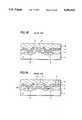
- a MOS (Metal Oxide Semiconductor) type field effect transistor having the n conductivity type(hereinafter referred to as "nMOSFET") is formed of a p-type single crystal silicon substrate 1, an insulation oxide film 2, a gate electrode 3 formed of polycrystalline silicon, a conductive interconnection 4 formed of tungsten silicide and source/drain regions 5 doped with n-type impurities.
- nMOSFETMetal Oxide Semiconductor type field effect transistor having the n conductivity type
- a BPSG (Boro-Phospho Silicate Glass) film 6 including a large amount of boron and phosphorusis deposited on the nMOSFET by CVD and annealed in an atmosphere including oxygen at 900° C. for 30 minutes to planarize BPSG film 6 as shown in FIG. 18.
- a hole having a cross section 10 ⁇ m squareis made in BPSG film 6 on conductive interconnection 4, where tungsten 7 is filled. Tungsten 7 is formed by selective CVD. The manufacturing process in a wafer state of pMOSFET (A) is thus completed.
- a pMOSFET (B)is formed by the same process as that shown in FIGS. 17 to 19.
- the pMOSFET (B)includes an insulation oxide film 12 formed on an n-type single crystalline silicon substrate 11, a gate electrode 13, a conductive interconnection 14 and source/drain regions 15 doped with p-type impurities, with tungsten 17 formed in a BPSG film 16 coinciding with tungsten 7 when placed face to face with nMOSFET (A) as shown in FIG. 20.
- nMOSFET (A) and pMOSFET (B)are put together by pressing, facing each other, and thermally treated in an electric furnace at 900° C. for 20 minutes to be stuck together. In this way, nMOSFET (A) and pMOSFET (B) are completely insulated and isolated from each other. As a result, a C (Complementary) MOSFET is constructed with a stacked-type structure including two layers.
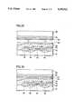
- a first layer of MOSFETis formed, including an insulation oxide film 22, a gate electrode 23, a conductive interconnection 24 and source/drain regions 25 on a single crystalline silicon substrate 21.
- an interlayer insulating film 26is deposited by CVD and the surface thereof is planarized by applying a resist and etching back.
- An aperture 27 having a cross section 1.3 ⁇ m square, extending to single crystalline silicon substrate 21,is made in part of interlayer insulating film 26 in order to form a single crystalline silicon layer on interlayer insulating film 26, which has the same crystal axis as that of single crystalline silicon substrate 21.
- polycrystalline silicon 28ais filled in aperture 27 by CVD and etching back.
- Polycrystalline silicon 29having a thickness of 0.5 ⁇ m is formed over interlayer insulating film 26 by CVD.
- polycrystalline silicon 29is irradiated with an argon laser beam 30 having a beam diameter of 100 ⁇ m moving in a direction indicated by the arrow in the figure at a scanning rate of 25 cm/s.
- Polycrystalline silicon 29becomes fused silicon 31 by the irradiation with the argon laser beam 30 and solidified and recrystallized after the irradiation is completed.
- fused silicon 31When fused silicon 31 is solidified, then epitaxial growth is caused in the lateral direction with single crystalline silicon substrate 21 and fused polycrystalline silicon 28a serving as a seed, polycrystalline silicon 28a becomes single crystallized silicon 28, and polycrystalline silicon 29 on interlayer insulating film 26 becomes single crystallized silicon 32 having the same crystal axis as that of single crystalline silicon substrate 21 (see FIG. 24).
- single crystallized silicon 32is patterned into single crystallized silicon 33 where a MOS transistor is to be formed and single crystallized silicon 34 on aperture 27 by photolithography and etching technique.
- a MOS transistor in a second layeris formed on single crystallized silicon 33 in the same way as that of the MOS transistor in the first layer (see FIG. 26).
- the MOS transistor in the second layerincludes an insulation oxide film 42, a gate electrode 43, a conductive interconnection 44 and source/drain regions 45.
- P-type single crystalline silicon substrate 1 and n-type single crystalline silicon substrate 11both must have a certain strength as they serve as substrates for supporting the devices during the manufacturing processes. Accordingly, they must be 500 to 600 ⁇ m thick.
- a reduction projection allignerwhich is mainly used at present, carries out mask alignment using a helium neon laser beam having a wavelength of 6428 ⁇ as a probe beam. Use of the helium neon laser beam as the probe beam enables mask alignment with positional accuracy of 0.3 ⁇ m.
- the helium neon lasercannot be used as the probe beam in the process of joining the substrates together since each substrate is at least 500 ⁇ m thick and the beam with the wavelength of 6428 ⁇ cannot be transmitted through such a substrate. Accordingly, in the process of joining the substrates together it was necessary to use infrared rays with a wavelength of 2.0 ⁇ m capable of being transmitted through a wafer of 500 ⁇ m in positioning each single crystalline silicon substrate. As a beam having a long wave length must be used, the positional accuracy in joining the single crystalline silicon substrates together was normally ⁇ 5 ⁇ m, and in the order of ⁇ 2 ⁇ m at best.
- the size of contact for connecting the substratesmust be above 10 ⁇ m making an allowance for the joining. Accordingly, in forming a CMOS by sticking the substrates together, it was impossible to increase the integration density of the elements up to the present LSI's level.
- the second background art methodhad a problem that, as it included a step of fusing and recrystallizing the polycrystalline silicon layer by the argon laser beam, an intense heat was generated, causing an adverse effect on the characteristics of the devices which had already been formed in the previous processes.
- Another possible method of manufacturing a stacked-type semiconductor device like the second background art method described abovemay be to fix a silicon substrate on the interlayer insulating layer by an adhesive material such as an epoxy resin and form a device on the silicon substrate (for example, see IEDM 85, pp. 684-686).
- an adhesive materialsuch as an epoxy resin
- interfacial statesare generated in the interface between the silicon substrate and the interlayer insulating layer, so that the potential of the silicon substrate is changed, degrading the device characteristics.
- An object of the present inventionis to provide a method of manufacturing a stacked-type semiconductor device where two or more semiconductor substrates can be joined together with a high accuracy by thermal treatment at such a low temperature as will not cause an adverse effect on a device already formed in the previous process.
- Another object of the present inventionis to improve the accuracy of joining devices in upper and lower layers of a stacked-type semiconductor device and increase its integration density.
- a first deviceis formed on a main surface of a first semiconductor substrate and the first device is covered with an interlayer insulating layer. Thereafter, the interlayer insulating layer is covered with a layer including silicon crystal and then the layer including the silicon crystal is planarized. Then, a refractory metal layer is formed on a main surface of a second semiconductor substrate. The surface of the refractory metal layer and the planarized surface of the layer including the silicon crystal are brought in close contact with each other and thermally treated at 700° C. or below. This thermal treatment changes the refractory metal layer to silicide, thereby joining the first semiconductor substrate and the second semiconductor substrate together.
- the above-described objectcan also be achieved by forming a silicon nitride film layer including a higher percentage of nitrogen than Si 3 N 4 on the main surface of the second semiconductor substrate, putting the silicon nitride film layer in close contact with the planarized layer including silicon crystal and applying thermal treatment at 700° C. or below.
- the first semiconductor substrate and the second semiconductor substratecan be joined together at a relatively low temperature of 700° C. or below, it is possible to avoid degradation of the device characteristic, which is involved in thermal diffusion of doped impurities into the first device already formed before the joining process.
- a method of manufacturing a stacked-type semiconductor device for achieving the latter object aboveincludes a process of predetermined grinding of the other main surface of the second semiconductor device and forming a second device on the other main surface after joining the first semiconductor substrate and the second semiconductor substrate together in accordance with either of the manufacturing methods described above for achieving the former object.
- the method of manufacturing the stacked-type semiconductor device according to the present inventionincludes a method where a main surface of the second semiconductor substrate is fixed on the first semiconductor substrate according to either of the manufacturing methods for achieving the former object above, and the a device is formed on the other main surface of the second semiconductor substrate.
- the second semiconductor substratecan be used as a supporting substrate and a second device can be formed on a semiconductor layer obtained by polishing the first semiconductor substrate. Accordingly, the semiconductor layer where the second device is to be formed can be made thin, enabling positioning with a high accuracy using a helium neon laser beam as a probe beam. As a result, positioning of the semiconductor substrates to be stuck together becomes relatively easy and its integration density can be increased.
- FIG. 1is a cross-sectional view of a CMOSFET formed by a method of manufacturing a stacked-type semiconductor device according to a first embodiment of the present invention (cross-sectional view taken along the line I--I in FIG. 2).
- FIG. 2is a plan view of the CMOSFET shown in FIG. 1.
- FIG. 3is a cross-sectional view taken along the line II--II in FIG. 2.
- FIG. 4is an equivalent circuit diagram of the CMOSFET shown in FIGS. 1 to 3.
- FIGS. 5, 6, 7, 8, 9 and 10are cross-sectional views showing in order each process in the method of manufacturing the stacked-type semiconductor device according to the first embodiment of the present invention.
- FIGS. 11, 12, 13, 14, 15 and 16are cross-sectional views showing in order each process in a method of manufacturing a stacked-type semiconductor device according to a third embodiment of the present invention.
- FIGS. 17, 18, 19, 20 and 21are cross-sectional views showing in order each process in a method of manufacturing a stacked-type semiconductor device according to a first example of the background art.
- FIGS. 22, 23, 24, 25 and 26are cross-sectional views showing in order each process in a method of manufacturing a stacked-type semiconductor device according to a second example of the background art.
- FIGS. 27, 28, 29, and 30are cross-sectional views showing in order each process in a method of manufacturing a stacked-type semiconductor device having a portion modified of the first embodiment.
- FIGS. 31, 32, 33, and 34are cross-sectional views showing in order each process in a method of manufacturing a stacked-type semiconductor device having a portion modified of the third embodiment.
- FIGS. 5 to 10A method of manufacturing a stacked-type semiconductor device according to a first embodiment of the present invention will now be described with reference to FIGS. 5 to 10.
- a first semiconductor layer 53 formed of single crystalline silicon having a thickness of about 1000 ⁇is formed over a main surface of a first semiconductor substrate 51 formed of single crystalline silicon with a first insulating layer 52 having a thickness of about 5000 ⁇ interposed therebetween.
- SOISilicon on Insulator
- SIMOXSeparation by Implanted Oxygen
- the above-described SOI structurecan be obtained by implanting oxygen ions into the main surface of first semiconductor substrate 51 with an accelerating voltage of about 180 KV and a dose of about 2 ⁇ 10 18 /cm 2 and annealing the entire wafer at about 1350° C. for about 1 hour.
- the thickness of first semiconductor layer 53 immediately after the annealingis in the order of 2000 ⁇ , it is adjusted to be in the order of 1000 ⁇ by oxidizing the surface of first semiconductor layer 53 in an atmosphere of vapor steam at about 950° C. and removing the oxide film by etching. Thereafter, the first semiconductor layer 53 is patterned so that it remains only in an active region.
- a nMOSFET as a first deviceis completed by forming n-type source/drain regions 73 and a p-type channel region 74 in the first semiconductor layer 53 and, further forming a gate electrode 54, an insulation oxide film 55 and a conductive interconnection 56.
- the structure having a cross section shown in FIG. 5is obtained by further covering the entire wafer with an interlayer insulating layer 57 by CVD.
- An outline of processes for forming this nMOSFETis as follows. Firstly, an oxide film is formed having a thickness of about 300 ⁇ on first semiconductor layer 53 by thermal oxidation at 950° C. A silicon nitride film (Si 3 N 4 ) is then deposited having a thickness of about 500 ⁇ on the oxide film by applying low pressure CVD at 780° C. The silicon nitride film is then removed by photolithography and etching, leaving the silicon nitride on a region to be an active layer.
- boron for isolationis implanted into an isolation region with an accelerating voltage 10 KV and a dose of 9 ⁇ 10 13 /cm 2 , with a resist film used when the silicon nitride film was removed being left as it is. Then, after removing the resist, first semiconductor layer 53 except the region to be the active layer is changed to an oxide film by oxidation in an atmosphere of vapor steam at 950° C. After that, boron is implanted into the first semiconductor layer 53 with an accelerating voltage of 20 KV and a dose of 5 ⁇ 10 11 /cm 2 , causing the first semiconductor layer 53 to have the p conductivity type.
- polycrystalline siliconis deposited on it, and furthermore, boron is implanted into the polycrystalline silicon with 20 KV and 1 ⁇ 10 16 /cm 2 . Then, this polycrystalline silicon is patterned to form gate electrode 54. Phosphorus is then implanted with 50 KV and 1 ⁇ 10 13 /cm 2 to form an n - region in the first semiconductor layer 53 and n-type source/drain regions 73 are formed by further implanting arsenic with 50 KV and 2 ⁇ 10 15 /cm 2 .
- insulation oxide film 55 covering gate electrode 54prevents the arsenic from being implanted into the n - region and channel region 74 of the first semiconductor layer 53.
- the n - regionis provided for mitigating the field strength of a portion of the drain region close to the channel region and has a so-called LDD (Lightly Doped Drain) structure.
- Interlayer insulating layer 57 formed of an oxide film having a thickness of 5000 ⁇is provided on thus formed nMOSFET serving as the first device by CVD.
- polycrystalline silicon having a thickness of about 1 ⁇ mis deposited over the entire surface of interlayer insulating layer 57 covering the nMOSFET as the first device, the surface thereof is planarized by rigid grinding to form a polycrystalline silicon layer 58 as shown in the cross-sectional view of FIG. 6.
- the rigid grinding method used in the planarization step of polycrystalline silicon layer 58is a method of carrying out a grinding process by abutting the grinding face of a hard pad having a planar grinding surface against the face of the workpiece to be ground. Because the conventional method of rotating a soft pad to grind the workpiece with its periphery is easily affected by the variation in the hardness of the surface to be ground of the workpiece, a favorable planarization was difficult to obtain. In contrary, the method of rigid grinding is not so affected by the variation in the hardness of the face of the workpiece to be ground to result in a ground workpiece face of a desired planarization.
- an oxide film 60 having a thickness of about 1000 ⁇is formed on a main surface of a second semiconductor substrate 59 formed of single crystalline silicon.
- refractory metal layer 61 and polycrystalline silicon layer 58are placed facing to each other as shown in FIG. 7 and, furthermore, put in close contact with each other and thermally treated in an atmosphere of nitrogen at 650° C. for 20 minutes.
- This thermal treatmentcauses refractory metal layer 61 formed of tungsten and polycrystalline silicon layer 58 to chemically react to produce a refractory metal silicide layer 62.
- the first semiconductor wafer and second semiconductor waferare joined together (see FIG. 8).
- first semiconductor substrate 51is then ground as far as the broken line in FIG. 8 by rigid grinding to form a second semiconductor layer 51a in the order of 1000 ⁇ as shown in FIG. 9.
- the second semiconductor layer 51ais patterned by photolithography and etching and, furthermore, a gate electrode 63 and an insulation oxide film 64 are formed. Thereafter, a contact hole 66 for the second semiconductor layer 51a and a contact hole 67 for conductive interconnection 56 of the previously formed nMOSFET are made. Then, a pMOSFET is formed on the second semiconductor layer 51a, and furthermore, a conductive interconnection 65 formed of aluminum or the like is provided. The pMOSFET and the nMOSFET are electrically connected to each other through contact hole 67.
- the substratesare stuck together by taking advantage of the chemical reaction between refractory metal layer 61 and polycrystalline silicon layer 58.
- This chemical reactionis caused at about 650° C., which is lower than in the background art method of joining the substrates.
- Such a degree of temperaturedoes not cause electrically active impurities doped in the device to diffuse again. Therefore, a stacked-type semiconductor integrated circuit can be made without degrading the characteristics of a device which has already been formed.
- the polycrystalline siliconmay be stuck on another tungsten silicide (W x Siy: y/x ⁇ 2) including less silicon than the chemical equivalent of the tungsten silicide (WSi 2 ) used in the above embodiment.
- W x Siy: y/x ⁇ 2another tungsten silicide
- silicon atomsmove from the polycrystalline silicon to get combined with the another tungsten silicide so that it is changed to the tungsten silicide (WSi 2 ) of the chemical equivalent by subsequent thermal treatment (including the thermal treatment in forming the device), and, as a result, the substrates are joined together.
- any refractory metalmay be used as far as it is silicidized at 700° C. or below and the melting point of the refractory metal silicide higher than the semiconductor process temperature.
- Table 1shows melting points and formation temperatures of various refractory metal silicides.
- silicideis formed at a temperature of about 600° C. and its melting point is higher than the temperature in the range of 900° C. to 1000° C. which is used in the semiconductor processes, it is possible to stick together substrates having devices formed thereon, using these substances indicated above.
- a refractory metal layermay be provided over the first semiconductor substrate 51 and a polycrystalline silicon layer may be provided over the second semiconductor substrate 59.
- quartz (pure SiO 2 ) substratemay be used.
- the pMOSFETis formed after the nMOSFET in the embodiment above, the order of formation may be reversed. Additionally, the same effects can be achieved as long as the device to be formed is a semiconductor element such as a bipolar transistor.
- a refractory metal layer 161is formed on the surface of interlayer insulation layer 57 to have its surface planarized by rigid grinding (FIG. 27). Then, a second semiconductor substrate 59 having a polycrystalline silicon layer 58 formed on a main surface with an oxide film 60 therebetween is moved as shown in FIG. 28 so that the surface of polycrystalline silicon layer 58 and the planarized surface of refractory metal layer 61 are adhered to each other. Under this condition, thermal treatment is carried out for twenty minutes at 650° C.
- a stacked-type semiconductor devicehaving a structure similar to that of FIG. 10 can be obtained.
- Arsenicis implanted into the polycrystalline silicon of gate electrode 63 with 50 KV and 5 ⁇ 10 15 /cm 2 to make gate electrode 63 of the n conductivity type. Then, boron is implanted into second semiconductor layer 51a with 20 KV and 1 ⁇ 10 13 /cm 2 to form a p - region and provide spacers on sidewalls of gate electrode 63. Thereafter, boron is implanted with 20 KV and 5 ⁇ 10 14 /cm 2 to form a p + region. Contact hole 66 and so on are made, furthermore, aluminum is deposited by sputtering, having 10000 ⁇ and patterned to form conductive interconnection 65, so that the pMOSFET is completed.
- FIGS. 1 to 3show the CMOSFET in detail.
- FIG. 4shows an equivalent circuit of the CMOSFET.
- FIGS. 2 and 3show a contact hole 71 for a conductive interconnection 77 connected to an input terminal and a gate electrode 54 and a contact hole 72 for a conductive interconnection 77 and a gate electrode 63.
- a descriptionwill now be made of a process of forming a conductive interconnection 65 on the upper layer side shown in FIGS. 1 to 3.
- a contact hole 66 having a diameter of 1 ⁇ mis apertured in an insulation oxide film 64 on a second semiconductor layer 51a.
- titaniumis deposited by sputtering to have a thickness of 500 ⁇ and annealing is carried out by an infrared ray lamp heating furnace in an atmosphere of nitrogen at 800° C. for 60 seconds.
- This treatmentchanges the titanium in contact with the single crystalline silicon to titanium silicide (TiSi 2 ) and other titanium is changed to titanium nitride (TIN).
- tungsten silicide (WSi 2 )is deposited by sputtering to have a thickness of 3000 ⁇ .
- the titanium nitride and the tungsten silicideare patterned to form a barrier metal layer 69 and conductive interconnection 65.
- the titanium silicideis formed for providing an ohmic contact between source/drain region 75 and conductive interconnection 65.
- the titanium nitrideserves as a barrier metal for preventing diffusion of the impurities implanted in the second semiconductor layer 51a into conductive interconnection 65.
- a conductive interconnection 56 and a barrier metal layer 70can be formed of the same materials and in the same processes as conductive interconnection 65 and barrier metal layer 69.
- the process of joining the first semiconductor substrate and the second semiconductor substrateis carried out at a relatively low temperature of 700° C. or below, degradation of the device characteristics due to the thermal treatment can be avoided.
- the helium neon laser beamis fully transmitted through the layer, reaching a mask alignment pattern (not shown) formed in the lower nMOSFET layer.
- the helium neon laser beam reflected from the mask alignment patternis strong enough to be detected even after it is transmitted through the second semiconductor layer 51a. Accordingly, it is possible to make a contact hole having a diameter in the approximate range of 0.8 to 1 ⁇ m with a mask alignment accuracy of ⁇ 0.3 ⁇ m and elements of high density can be manufactured using a reduced projection exposing apparatus which gives the highest resolution and positional accuracy at present.
- a silicon nitride film(Si x N y : y/x is at least 1.33 and preferably 1.4) containing a larger amount of nitrogen than the chemical equivalent (Si 3 N 4 ), instead of refractory metal layer 61, is formed over a main surface of a second semiconductor substrate 59 to have a thickness of 1000 ⁇ with an insulating layer 60 interposed therebetween.
- This silicon nitride filmis deposited by ECR (Electron Cyclotron Resonance)-CVD. The depositing temperature is in the order of 100° C.
- the surface of the silicon nitride film layer of the second semiconductor substrate 59 formed in this wayis put face to face with and in close contact with a planarized surface of a polycrystalline silicon layer 58 of a first semiconductor substrate 51 and both of them are heated in an atmosphere of nitrogen at 700° C. or below.
- the silicon nitride film(Si x Ny) absorbs silicon atoms from polycrystalline silicon layer 58 in order to attain a composition of the chemical equivalent. This chemical reaction enables to join the first semiconductor substrate 51 and the second semiconductor substrate 59 together.
- Other processesare the same as those in the first embodiment above.
- the manufacturing method of this embodimentsince the first semiconductor substrate 51 and the second semiconductor substrate 59 can be joined together by thermal treatment at a relatively low temperature of 700° C. or below, an adverse effect of the heat on the first device formed in the previous process can be avoided.
- a silicon nitride filmis formed at the side of the second semiconductor substrate 59 and a polycrystalline silicon layer 58 is formed at the side of the first semiconductor substrate 51 in the present embodiment, a same effect can be obtained by forming a planarized silicon nitride film at the side of the first semiconductor substrate 51, and a polycrystalline silicon layer at the side of second semiconductor substrate 59 to be bonded together.
- FIGS. 11 to FIG. 15A third embodiment according to the present invention will now be described with reference to FIGS. 11 to FIG. 15.
- This embodimentcan be compared with the second example of the background art described before and relates to a manufacturing method where another device is stacked over a semiconductor substrate having a device already formed thereon.
- a MOSFET serving as a first deviceis provided on a first semiconductor substrate 81 formed of single crystalline silicon, including an insulation oxide film 82, a gate electrode 83, a conductive interconnection 84 and source/drain regions 85.
- This MOSFETis covered with an interlayer insulating layer 86 having a thickness of about 5000 ⁇ by CVD and, furthermore, a polycrystalline silicon layer 87 is formed also by CVD to have a thickness of about 1 ⁇ m (see FIG. 12). Thereafter, the upper surface of polycrystalline silicon layer 87 is planarized by rigid grinding (see FIG. 13).
- a refractory metal layer 90 formed of tungsten or the likeis deposited over a main surface of a second semiconductor substrate 88 formed of single crystalline silicon to have a thickness of about 3000 ⁇ by sputtering with an insulating layer 89 interposed therebetween. Thereafter, as shown in FIG. 14, the surfaces of refractory metal layer 90 and polycrystalline silicon layer 87 are put face to face and in close contact with each other.
- thermal treatment in an atmosphere of nitrogen at 650° C. for 20 minutesis carried out to cause reaction between polycrystalline silicon layer 87 and refractory metal layer 90 to change refractory metal layer 90 to a refractory metal silicide layer 91 so that they are joined together (see FIG. 15).
- a second deviceis formed on a main surface on the opposite side of insulating layer 89 of the second semiconductor substrate 88 as shown in FIG. 16.
- the second deviceincludes an insulation oxide film 92, a gate electrode 93, a conductive interconnection 94 and source/drain regions 95.
- this manufacturing methodcan provide a device having a structure where a plurality of layers are stacked up without degrading the device characteristics.
- planarized polycrystalline silicon layer 87 and refractory metal layer 90are put in close contact with each other to be joined together in this embodiment, of course, the same effects can be achieved by depositing a silicon nitride film, instead of refractory metal layer 90, containing a larger amount of nitrogen than the chemical equivalent (Si 3 N 4 ) and applying the same thermal treatment as in the second embodiment described above.
- the present embodimenthas a planarized polycrystalline silicon layer 87 formed at the side of the first semiconductor substrate 81, and a refractory metal layer 90 formed at the side of the second semiconductor substrate 88, the steps shown in FIGS. 31-34 are also possible.
- refractory metal layer 190is formed on the surface of interlayer insulating film 86 (FIG. 31), whereby the surface is planarized by rigid grinding (FIG. 32).
- a second semiconductor substrate 88 having a polycrystalline silicon layer 187 formed on the main surface with an oxide film 89 therebetweenis moved to the surface of refractory metal layer 190 shown in FIG.
- CMOSComplementary Metal Oxide Semiconductor
- a stacked-type semiconductor devicecan be manufactured without causing an adverse effect of heat on a device formed in the previous process.
- the back surface of the first semiconductor substrateis polished and has a second device formed thereon, so that aligning using the helium neon laser beam as a probe beam is made possible and a stacked-type semiconductor device with high integration density can be manufactured.
Landscapes
- Engineering & Computer Science (AREA)
- Physics & Mathematics (AREA)
- Condensed Matter Physics & Semiconductors (AREA)
- General Physics & Mathematics (AREA)
- Manufacturing & Machinery (AREA)
- Computer Hardware Design (AREA)
- Microelectronics & Electronic Packaging (AREA)
- Power Engineering (AREA)
- Thin Film Transistor (AREA)
- Metal-Oxide And Bipolar Metal-Oxide Semiconductor Integrated Circuits (AREA)
- Internal Circuitry In Semiconductor Integrated Circuit Devices (AREA)
Abstract
Description
TABLE 1 ______________________________________ Melting points and formation temperatures of various refractory metal silicides Silicide Melting point formation Substance (°C.) temperature (°C.) ______________________________________ TiSi.sub.2 1540 600 VSi.sub.2 1670 600 CrSi.sub.2 1550 450 ZrSi.sub.2 1650 700 NbSi.sub.2 1950 650 MoSi.sub.2 1980 525 HfSi.sub.2 1800 700 TaSi.sub.2 2200 650 WSi.sub.2 2165 650 ______________________________________
Claims (10)
Priority Applications (1)
| Application Number | Priority Date | Filing Date | Title |
|---|---|---|---|
| US08/222,502US5504376A (en) | 1991-09-10 | 1994-04-04 | Stacked-type semiconductor device |
Applications Claiming Priority (4)
| Application Number | Priority Date | Filing Date | Title |
|---|---|---|---|
| JP23024691 | 1991-09-10 | ||
| JP3-230246 | 1991-09-10 | ||
| JP4-164593 | 1992-06-23 | ||
| JP16459392AJPH05198739A (en) | 1991-09-10 | 1992-06-23 | Stacked semiconductor device and manufacturing method thereof |
Related Child Applications (1)
| Application Number | Title | Priority Date | Filing Date |
|---|---|---|---|
| US08/222,502ContinuationUS5504376A (en) | 1991-09-10 | 1994-04-04 | Stacked-type semiconductor device |
Publications (1)
| Publication Number | Publication Date |
|---|---|
| US5355022Atrue US5355022A (en) | 1994-10-11 |
Family
ID=26489629
Family Applications (2)
| Application Number | Title | Priority Date | Filing Date |
|---|---|---|---|
| US07/936,390Expired - LifetimeUS5355022A (en) | 1991-09-10 | 1992-08-28 | Stacked-type semiconductor device |
| US08/222,502Expired - LifetimeUS5504376A (en) | 1991-09-10 | 1994-04-04 | Stacked-type semiconductor device |
Family Applications After (1)
| Application Number | Title | Priority Date | Filing Date |
|---|---|---|---|
| US08/222,502Expired - LifetimeUS5504376A (en) | 1991-09-10 | 1994-04-04 | Stacked-type semiconductor device |
Country Status (4)
| Country | Link |
|---|---|
| US (2) | US5355022A (en) |
| JP (1) | JPH05198739A (en) |
| DE (1) | DE4229628C2 (en) |
| FR (1) | FR2682811B1 (en) |
Cited By (270)
| Publication number | Priority date | Publication date | Assignee | Title |
|---|---|---|---|---|
| US5504376A (en)* | 1991-09-10 | 1996-04-02 | Mitsubishi Denki Kabushiki Kaisha | Stacked-type semiconductor device |
| US5523602A (en)* | 1993-09-06 | 1996-06-04 | Hitachi, Ltd. | Multi-layered structure having single crystalline semiconductor film formed on insulator |
| US5929488A (en)* | 1994-04-05 | 1999-07-27 | Kabushiki Kaisha Toshiba | Metal-oxide semiconductor device |
| US5985739A (en)* | 1994-09-19 | 1999-11-16 | Fraunhofer-Gesellschaft Zur Forderung Der Angewandten Forschung E.V. | Semiconductor structures having advantageous high-frequency characteristics and processes for producing such semiconductor structures |
| US6004865A (en)* | 1993-09-06 | 1999-12-21 | Hitachi, Ltd. | Method of fabricating multi-layered structure having single crystalline semiconductor film formed on insulator |
| US6426248B2 (en)* | 2000-02-15 | 2002-07-30 | International Rectifier Corporation | Process for forming power MOSFET device in float zone, non-epitaxial silicon |
| US6744116B1 (en)* | 1998-06-30 | 2004-06-01 | Intel Corporation | Thin film using non-thermal techniques |
| US20050127525A1 (en)* | 2003-12-15 | 2005-06-16 | Alie Susan A. | Semiconductor assembly with conductive rim and method of producing the same |
| US20050170609A1 (en)* | 2003-12-15 | 2005-08-04 | Alie Susan A. | Conductive bond for through-wafer interconnect |
| US20050280155A1 (en)* | 2004-06-21 | 2005-12-22 | Sang-Yun Lee | Semiconductor bonding and layer transfer method |
| US20050280154A1 (en)* | 2004-06-21 | 2005-12-22 | Sang-Yun Lee | Semiconductor memory device |
| US20060166480A1 (en)* | 2004-06-02 | 2006-07-27 | Analog Devices, Inc. | Interconnection of through-wafer vias using bridge structures |
| US20060170046A1 (en)* | 2005-01-31 | 2006-08-03 | Fujitsu Limited | Semiconductor device and manufacturing method thereof |
| US20070018164A1 (en)* | 2000-09-14 | 2007-01-25 | Semiconductor Energy Laboratory Co., Ltd. | Semiconductor Device and Manufacturing Method Thereof |
| US20080048327A1 (en)* | 2004-06-21 | 2008-02-28 | Sang-Yun Lee | Electronic circuit with embedded memory |
| US20080061419A1 (en)* | 1999-10-01 | 2008-03-13 | Ziptronix | Three dimensional device integration method and integrated device |
| US20080090344A1 (en)* | 2001-11-16 | 2008-04-17 | Semiconductor Energy Laboratory Co., Ltd. | Semiconductor device and manufacturing method thereof |
| US20080087979A1 (en)* | 2006-10-13 | 2008-04-17 | Analog Devices, Inc. | Integrated Circuit with Back Side Conductive Paths |
| US20080116566A1 (en)* | 2006-11-22 | 2008-05-22 | Shinko Electric Industries Co., Ltd. | Electronic component and method for manufacturing the same |
| US20080168838A1 (en)* | 2007-01-11 | 2008-07-17 | Analog Devices, Inc. | MEMS Sensor with Cap Electrode |
| US20080191312A1 (en)* | 2003-06-24 | 2008-08-14 | Oh Choonsik | Semiconductor circuit |
| US20090111241A1 (en)* | 2003-06-24 | 2009-04-30 | Sang-Yun Lee | Wafer bonding method |
| US20090224364A1 (en)* | 2003-06-24 | 2009-09-10 | Oh Choonsik | Semiconductor circuit and method of fabricating the same |
| US20090250736A1 (en)* | 2008-04-08 | 2009-10-08 | Jae-Man Yoon | Semiconductor device |
| US20090325343A1 (en)* | 2003-06-24 | 2009-12-31 | Sang-Yun Lee | Bonded semiconductor structure and method of fabricating the same |
| US20100038743A1 (en)* | 2003-06-24 | 2010-02-18 | Sang-Yun Lee | Information storage system which includes a bonded semiconductor structure |
| US20100059835A1 (en)* | 2008-09-10 | 2010-03-11 | Analog Devices, Inc. | Apparatus and Method of Wafer Bonding Using Compatible Alloy |
| US20100133695A1 (en)* | 2003-01-12 | 2010-06-03 | Sang-Yun Lee | Electronic circuit with embedded memory |
| US20100190334A1 (en)* | 2003-06-24 | 2010-07-29 | Sang-Yun Lee | Three-dimensional semiconductor structure and method of manufacturing the same |
| US20100256918A1 (en)* | 2009-03-11 | 2010-10-07 | Industrial Technology Research Institute | Apparatus and method for detection and discrimination molecular object |
| US7863619B2 (en) | 1993-10-01 | 2011-01-04 | Semiconductor Energy Laboratory Co., Ltd. | Semiconductor device and a method for manufacturing the same |
| US20110003438A1 (en)* | 2005-03-29 | 2011-01-06 | Sang-Yun Lee | Three-dimensional integrated circuit structure |
| US7867822B2 (en) | 2003-06-24 | 2011-01-11 | Sang-Yun Lee | Semiconductor memory device |
| US20110053332A1 (en)* | 2003-06-24 | 2011-03-03 | Sang-Yun Lee | Semiconductor circuit |
| US7927975B2 (en) | 2009-02-04 | 2011-04-19 | Micron Technology, Inc. | Semiconductor material manufacture |
| US20110143506A1 (en)* | 2009-12-10 | 2011-06-16 | Sang-Yun Lee | Method for fabricating a semiconductor memory device |
| US20110201151A1 (en)* | 2008-12-24 | 2011-08-18 | International Business Machines Corporation | Methods for forming a bonded semiconductor substrate including a cooling mechanism |
| US8058142B2 (en) | 1996-11-04 | 2011-11-15 | Besang Inc. | Bonded semiconductor structure and method of making the same |
| US8203148B2 (en) | 2010-10-11 | 2012-06-19 | Monolithic 3D Inc. | Semiconductor device and structure |
| US8237228B2 (en) | 2009-10-12 | 2012-08-07 | Monolithic 3D Inc. | System comprising a semiconductor device and structure |
| US8273610B2 (en) | 2010-11-18 | 2012-09-25 | Monolithic 3D Inc. | Method of constructing a semiconductor device and structure |
| US8294159B2 (en) | 2009-10-12 | 2012-10-23 | Monolithic 3D Inc. | Method for fabrication of a semiconductor device and structure |
| US8362482B2 (en) | 2009-04-14 | 2013-01-29 | Monolithic 3D Inc. | Semiconductor device and structure |
| US8362800B2 (en) | 2010-10-13 | 2013-01-29 | Monolithic 3D Inc. | 3D semiconductor device including field repairable logics |
| US8373230B1 (en) | 2010-10-13 | 2013-02-12 | Monolithic 3D Inc. | Method for fabrication of a semiconductor device and structure |
| US8373439B2 (en) | 2009-04-14 | 2013-02-12 | Monolithic 3D Inc. | 3D semiconductor device |
| US8378715B2 (en) | 2009-04-14 | 2013-02-19 | Monolithic 3D Inc. | Method to construct systems |
| US8379458B1 (en) | 2010-10-13 | 2013-02-19 | Monolithic 3D Inc. | Semiconductor device and structure |
| US8378494B2 (en) | 2009-04-14 | 2013-02-19 | Monolithic 3D Inc. | Method for fabrication of a semiconductor device and structure |
| US8384426B2 (en) | 2009-04-14 | 2013-02-26 | Monolithic 3D Inc. | Semiconductor device and structure |
| US8405420B2 (en) | 2009-04-14 | 2013-03-26 | Monolithic 3D Inc. | System comprising a semiconductor device and structure |
| US8427200B2 (en) | 2009-04-14 | 2013-04-23 | Monolithic 3D Inc. | 3D semiconductor device |
| US8440542B2 (en) | 2010-10-11 | 2013-05-14 | Monolithic 3D Inc. | Semiconductor device and structure |
| US8450804B2 (en) | 2011-03-06 | 2013-05-28 | Monolithic 3D Inc. | Semiconductor device and structure for heat removal |
| US8455978B2 (en) | 2010-05-27 | 2013-06-04 | Sang-Yun Lee | Semiconductor circuit structure and method of making the same |
| US8461035B1 (en) | 2010-09-30 | 2013-06-11 | Monolithic 3D Inc. | Method for fabrication of a semiconductor device and structure |
| US8476145B2 (en) | 2010-10-13 | 2013-07-02 | Monolithic 3D Inc. | Method of fabricating a semiconductor device and structure |
| US8492886B2 (en) | 2010-02-16 | 2013-07-23 | Monolithic 3D Inc | 3D integrated circuit with logic |
| US8536023B2 (en) | 2010-11-22 | 2013-09-17 | Monolithic 3D Inc. | Method of manufacturing a semiconductor device and structure |
| US8541819B1 (en) | 2010-12-09 | 2013-09-24 | Monolithic 3D Inc. | Semiconductor device and structure |
| US8557632B1 (en) | 2012-04-09 | 2013-10-15 | Monolithic 3D Inc. | Method for fabrication of a semiconductor device and structure |
| US8574929B1 (en) | 2012-11-16 | 2013-11-05 | Monolithic 3D Inc. | Method to form a 3D semiconductor device and structure |
| US8581349B1 (en) | 2011-05-02 | 2013-11-12 | Monolithic 3D Inc. | 3D memory semiconductor device and structure |
| US8642416B2 (en) | 2010-07-30 | 2014-02-04 | Monolithic 3D Inc. | Method of forming three dimensional integrated circuit devices using layer transfer technique |
| US8669778B1 (en) | 2009-04-14 | 2014-03-11 | Monolithic 3D Inc. | Method for design and manufacturing of a 3D semiconductor device |
| US8674470B1 (en) | 2012-12-22 | 2014-03-18 | Monolithic 3D Inc. | Semiconductor device and structure |
| US8686428B1 (en) | 2012-11-16 | 2014-04-01 | Monolithic 3D Inc. | Semiconductor device and structure |
| US8687399B2 (en) | 2011-10-02 | 2014-04-01 | Monolithic 3D Inc. | Semiconductor device and structure |
| US8709880B2 (en) | 2010-07-30 | 2014-04-29 | Monolithic 3D Inc | Method for fabrication of a semiconductor device and structure |
| US8723335B2 (en) | 2010-05-20 | 2014-05-13 | Sang-Yun Lee | Semiconductor circuit structure and method of forming the same using a capping layer |
| US8742476B1 (en) | 2012-11-27 | 2014-06-03 | Monolithic 3D Inc. | Semiconductor device and structure |
| US8754533B2 (en) | 2009-04-14 | 2014-06-17 | Monolithic 3D Inc. | Monolithic three-dimensional semiconductor device and structure |
| US8753913B2 (en) | 2010-10-13 | 2014-06-17 | Monolithic 3D Inc. | Method for fabricating novel semiconductor and optoelectronic devices |
| US8803206B1 (en) | 2012-12-29 | 2014-08-12 | Monolithic 3D Inc. | 3D semiconductor device and structure |
| US8901613B2 (en) | 2011-03-06 | 2014-12-02 | Monolithic 3D Inc. | Semiconductor device and structure for heat removal |
| US8902663B1 (en) | 2013-03-11 | 2014-12-02 | Monolithic 3D Inc. | Method of maintaining a memory state |
| US8956904B2 (en) | 2008-09-10 | 2015-02-17 | Analog Devices, Inc. | Apparatus and method of wafer bonding using compatible alloy |
| US8975670B2 (en) | 2011-03-06 | 2015-03-10 | Monolithic 3D Inc. | Semiconductor device and structure for heat removal |
| CN104425443A (en)* | 2013-08-27 | 2015-03-18 | 台湾积体电路制造股份有限公司 | Semiconductor logic circuits fabricated using multi-layer structures |
| US8994404B1 (en) | 2013-03-12 | 2015-03-31 | Monolithic 3D Inc. | Semiconductor device and structure |
| US9000557B2 (en) | 2012-03-17 | 2015-04-07 | Zvi Or-Bach | Semiconductor device and structure |
| US9012292B2 (en) | 2010-07-02 | 2015-04-21 | Sang-Yun Lee | Semiconductor memory device and method of fabricating the same |
| US9029173B2 (en) | 2011-10-18 | 2015-05-12 | Monolithic 3D Inc. | Method for fabrication of a semiconductor device and structure |
| US9099526B2 (en) | 2010-02-16 | 2015-08-04 | Monolithic 3D Inc. | Integrated circuit device and structure |
| US9099424B1 (en) | 2012-08-10 | 2015-08-04 | Monolithic 3D Inc. | Semiconductor system, device and structure with heat removal |
| US9117749B1 (en) | 2013-03-15 | 2015-08-25 | Monolithic 3D Inc. | Semiconductor device and structure |
| US9197804B1 (en) | 2011-10-14 | 2015-11-24 | Monolithic 3D Inc. | Semiconductor and optoelectronic devices |
| US9219005B2 (en) | 2011-06-28 | 2015-12-22 | Monolithic 3D Inc. | Semiconductor system and device |
| US9509313B2 (en) | 2009-04-14 | 2016-11-29 | Monolithic 3D Inc. | 3D semiconductor device |
| US9577642B2 (en) | 2009-04-14 | 2017-02-21 | Monolithic 3D Inc. | Method to form a 3D semiconductor device |
| US9711407B2 (en) | 2009-04-14 | 2017-07-18 | Monolithic 3D Inc. | Method of manufacturing a three dimensional integrated circuit by transfer of a mono-crystalline layer |
| US9777321B2 (en) | 2010-03-15 | 2017-10-03 | Industrial Technology Research Institute | Single molecule detection system and methods |
| US9871034B1 (en) | 2012-12-29 | 2018-01-16 | Monolithic 3D Inc. | Semiconductor device and structure |
| US9953925B2 (en) | 2011-06-28 | 2018-04-24 | Monolithic 3D Inc. | Semiconductor system and device |
| US9995683B2 (en)* | 2010-06-11 | 2018-06-12 | Industrial Technology Research Institute | Apparatus for single-molecule detection |
| US10043781B2 (en) | 2009-10-12 | 2018-08-07 | Monolithic 3D Inc. | 3D semiconductor device and structure |
| US10115663B2 (en) | 2012-12-29 | 2018-10-30 | Monolithic 3D Inc. | 3D semiconductor device and structure |
| US10127344B2 (en) | 2013-04-15 | 2018-11-13 | Monolithic 3D Inc. | Automation for monolithic 3D devices |
| US10157909B2 (en) | 2009-10-12 | 2018-12-18 | Monolithic 3D Inc. | 3D semiconductor device and structure |
| US10217667B2 (en) | 2011-06-28 | 2019-02-26 | Monolithic 3D Inc. | 3D semiconductor device, fabrication method and system |
| US10224279B2 (en) | 2013-03-15 | 2019-03-05 | Monolithic 3D Inc. | Semiconductor device and structure |
| CN109643742A (en)* | 2016-08-26 | 2019-04-16 | 英特尔公司 | Integrated circuit device structure and double-sided fabrication technology |
| US10290682B2 (en) | 2010-10-11 | 2019-05-14 | Monolithic 3D Inc. | 3D IC semiconductor device and structure with stacked memory |
| US10297586B2 (en) | 2015-03-09 | 2019-05-21 | Monolithic 3D Inc. | Methods for processing a 3D semiconductor device |
| US10325651B2 (en) | 2013-03-11 | 2019-06-18 | Monolithic 3D Inc. | 3D semiconductor device with stacked memory |
| US10354995B2 (en) | 2009-10-12 | 2019-07-16 | Monolithic 3D Inc. | Semiconductor memory device and structure |
| US10366970B2 (en) | 2009-10-12 | 2019-07-30 | Monolithic 3D Inc. | 3D semiconductor device and structure |
| US10381328B2 (en) | 2015-04-19 | 2019-08-13 | Monolithic 3D Inc. | Semiconductor device and structure |
| US10388568B2 (en) | 2011-06-28 | 2019-08-20 | Monolithic 3D Inc. | 3D semiconductor device and system |
| US10388863B2 (en) | 2009-10-12 | 2019-08-20 | Monolithic 3D Inc. | 3D memory device and structure |
| US10418369B2 (en) | 2015-10-24 | 2019-09-17 | Monolithic 3D Inc. | Multi-level semiconductor memory device and structure |
| US20190319021A1 (en)* | 2018-04-17 | 2019-10-17 | International Business Machines Corporation | Perpendicular stacked field-effect transistor device |
| US10497713B2 (en) | 2010-11-18 | 2019-12-03 | Monolithic 3D Inc. | 3D semiconductor memory device and structure |
| US10515981B2 (en) | 2015-09-21 | 2019-12-24 | Monolithic 3D Inc. | Multilevel semiconductor device and structure with memory |
| US10522225B1 (en) | 2015-10-02 | 2019-12-31 | Monolithic 3D Inc. | Semiconductor device with non-volatile memory |
| US10600888B2 (en) | 2012-04-09 | 2020-03-24 | Monolithic 3D Inc. | 3D semiconductor device |
| US10600657B2 (en) | 2012-12-29 | 2020-03-24 | Monolithic 3D Inc | 3D semiconductor device and structure |
| US10651054B2 (en) | 2012-12-29 | 2020-05-12 | Monolithic 3D Inc. | 3D semiconductor device and structure |
| US10679977B2 (en) | 2010-10-13 | 2020-06-09 | Monolithic 3D Inc. | 3D microdisplay device and structure |
| US10825779B2 (en) | 2015-04-19 | 2020-11-03 | Monolithic 3D Inc. | 3D semiconductor device and structure |
| US10833108B2 (en) | 2010-10-13 | 2020-11-10 | Monolithic 3D Inc. | 3D microdisplay device and structure |
| US10840239B2 (en) | 2014-08-26 | 2020-11-17 | Monolithic 3D Inc. | 3D semiconductor device and structure |
| US10847540B2 (en) | 2015-10-24 | 2020-11-24 | Monolithic 3D Inc. | 3D semiconductor memory device and structure |
| US10892169B2 (en) | 2012-12-29 | 2021-01-12 | Monolithic 3D Inc. | 3D semiconductor device and structure |
| US10892016B1 (en) | 2019-04-08 | 2021-01-12 | Monolithic 3D Inc. | 3D memory semiconductor devices and structures |
| US10896931B1 (en) | 2010-10-11 | 2021-01-19 | Monolithic 3D Inc. | 3D semiconductor device and structure |
| US10903089B1 (en) | 2012-12-29 | 2021-01-26 | Monolithic 3D Inc. | 3D semiconductor device and structure |
| US10910364B2 (en) | 2009-10-12 | 2021-02-02 | Monolitaic 3D Inc. | 3D semiconductor device |
| US10943934B2 (en) | 2010-10-13 | 2021-03-09 | Monolithic 3D Inc. | Multilevel semiconductor device and structure |
| US10978501B1 (en) | 2010-10-13 | 2021-04-13 | Monolithic 3D Inc. | Multilevel semiconductor device and structure with waveguides |
| US10998374B1 (en) | 2010-10-13 | 2021-05-04 | Monolithic 3D Inc. | Multilevel semiconductor device and structure |
| US11004694B1 (en) | 2012-12-29 | 2021-05-11 | Monolithic 3D Inc. | 3D semiconductor device and structure |
| US11004719B1 (en) | 2010-11-18 | 2021-05-11 | Monolithic 3D Inc. | Methods for producing a 3D semiconductor memory device and structure |
| US11011507B1 (en) | 2015-04-19 | 2021-05-18 | Monolithic 3D Inc. | 3D semiconductor device and structure |
| US11018156B2 (en) | 2019-04-08 | 2021-05-25 | Monolithic 3D Inc. | 3D memory semiconductor devices and structures |
| US11018042B1 (en) | 2010-11-18 | 2021-05-25 | Monolithic 3D Inc. | 3D semiconductor memory device and structure |
| US11018191B1 (en) | 2010-10-11 | 2021-05-25 | Monolithic 3D Inc. | 3D semiconductor device and structure |
| US11018116B2 (en) | 2012-12-22 | 2021-05-25 | Monolithic 3D Inc. | Method to form a 3D semiconductor device and structure |
| US11018133B2 (en) | 2009-10-12 | 2021-05-25 | Monolithic 3D Inc. | 3D integrated circuit |
| US11024673B1 (en) | 2010-10-11 | 2021-06-01 | Monolithic 3D Inc. | 3D semiconductor device and structure |
| US11031394B1 (en) | 2014-01-28 | 2021-06-08 | Monolithic 3D Inc. | 3D semiconductor device and structure |
| US11030371B2 (en) | 2013-04-15 | 2021-06-08 | Monolithic 3D Inc. | Automation for monolithic 3D devices |
| US11031275B2 (en) | 2010-11-18 | 2021-06-08 | Monolithic 3D Inc. | 3D semiconductor device and structure with memory |
| US11043523B1 (en) | 2010-10-13 | 2021-06-22 | Monolithic 3D Inc. | Multilevel semiconductor device and structure with image sensors |
| US11056468B1 (en) | 2015-04-19 | 2021-07-06 | Monolithic 3D Inc. | 3D semiconductor device and structure |
| US11063024B1 (en) | 2012-12-22 | 2021-07-13 | Monlithic 3D Inc. | Method to form a 3D semiconductor device and structure |
| US11063071B1 (en) | 2010-10-13 | 2021-07-13 | Monolithic 3D Inc. | Multilevel semiconductor device and structure with waveguides |
| US11088050B2 (en) | 2012-04-09 | 2021-08-10 | Monolithic 3D Inc. | 3D semiconductor device with isolation layers |
| US11088130B2 (en) | 2014-01-28 | 2021-08-10 | Monolithic 3D Inc. | 3D semiconductor device and structure |
| US11087995B1 (en) | 2012-12-29 | 2021-08-10 | Monolithic 3D Inc. | 3D semiconductor device and structure |
| US11094576B1 (en) | 2010-11-18 | 2021-08-17 | Monolithic 3D Inc. | Methods for producing a 3D semiconductor memory device and structure |
| US11107808B1 (en) | 2014-01-28 | 2021-08-31 | Monolithic 3D Inc. | 3D semiconductor device and structure |
| US11107721B2 (en) | 2010-11-18 | 2021-08-31 | Monolithic 3D Inc. | 3D semiconductor device and structure with NAND logic |
| US11114427B2 (en) | 2015-11-07 | 2021-09-07 | Monolithic 3D Inc. | 3D semiconductor processor and memory device and structure |
| US11114464B2 (en) | 2015-10-24 | 2021-09-07 | Monolithic 3D Inc. | 3D semiconductor device and structure |
| US11121021B2 (en) | 2010-11-18 | 2021-09-14 | Monolithic 3D Inc. | 3D semiconductor device and structure |
| US11133344B2 (en) | 2010-10-13 | 2021-09-28 | Monolithic 3D Inc. | Multilevel semiconductor device and structure with image sensors |
| US11158674B2 (en) | 2010-10-11 | 2021-10-26 | Monolithic 3D Inc. | Method to produce a 3D semiconductor device and structure |
| US11158652B1 (en) | 2019-04-08 | 2021-10-26 | Monolithic 3D Inc. | 3D memory semiconductor devices and structures |
| US11164811B2 (en) | 2012-04-09 | 2021-11-02 | Monolithic 3D Inc. | 3D semiconductor device with isolation layers and oxide-to-oxide bonding |
| US11163112B2 (en) | 2010-10-13 | 2021-11-02 | Monolithic 3D Inc. | Multilevel semiconductor device and structure with electromagnetic modulators |
| US11164898B2 (en) | 2010-10-13 | 2021-11-02 | Monolithic 3D Inc. | Multilevel semiconductor device and structure |
| US11164770B1 (en) | 2010-11-18 | 2021-11-02 | Monolithic 3D Inc. | Method for producing a 3D semiconductor memory device and structure |
| US11177140B2 (en) | 2012-12-29 | 2021-11-16 | Monolithic 3D Inc. | 3D semiconductor device and structure |
| US11211279B2 (en) | 2010-11-18 | 2021-12-28 | Monolithic 3D Inc. | Method for processing a 3D integrated circuit and structure |
| US11217565B2 (en) | 2012-12-22 | 2022-01-04 | Monolithic 3D Inc. | Method to form a 3D semiconductor device and structure |
| US11227897B2 (en) | 2010-10-11 | 2022-01-18 | Monolithic 3D Inc. | Method for producing a 3D semiconductor memory device and structure |
| US11251149B2 (en) | 2016-10-10 | 2022-02-15 | Monolithic 3D Inc. | 3D memory device and structure |
| US11257867B1 (en) | 2010-10-11 | 2022-02-22 | Monolithic 3D Inc. | 3D semiconductor device and structure with oxide bonds |
| US11270055B1 (en) | 2013-04-15 | 2022-03-08 | Monolithic 3D Inc. | Automation for monolithic 3D devices |
| US11296106B2 (en) | 2019-04-08 | 2022-04-05 | Monolithic 3D Inc. | 3D memory semiconductor devices and structures |
| US11296115B1 (en) | 2015-10-24 | 2022-04-05 | Monolithic 3D Inc. | 3D semiconductor device and structure |
| US11309292B2 (en) | 2012-12-22 | 2022-04-19 | Monolithic 3D Inc. | 3D semiconductor device and structure with metal layers |
| US11315980B1 (en) | 2010-10-11 | 2022-04-26 | Monolithic 3D Inc. | 3D semiconductor device and structure with transistors |
| US20220130846A1 (en)* | 2020-10-28 | 2022-04-28 | Samsung Electronics Co., Ltd. | Semiconductor device having peripheral circuit areas at both sides of substrate and data storage system including the same |
| US11329059B1 (en) | 2016-10-10 | 2022-05-10 | Monolithic 3D Inc. | 3D memory devices and structures with thinned single crystal substrates |
| US11327227B2 (en) | 2010-10-13 | 2022-05-10 | Monolithic 3D Inc. | Multilevel semiconductor device and structure with electromagnetic modulators |
| US11328951B2 (en) | 2016-04-01 | 2022-05-10 | Intel Corporation | Transistor cells including a deep via lined wit h a dielectric material |
| US11341309B1 (en) | 2013-04-15 | 2022-05-24 | Monolithic 3D Inc. | Automation for monolithic 3D devices |
| US11355380B2 (en) | 2010-11-18 | 2022-06-07 | Monolithic 3D Inc. | Methods for producing 3D semiconductor memory device and structure utilizing alignment marks |
| US11355381B2 (en) | 2010-11-18 | 2022-06-07 | Monolithic 3D Inc. | 3D semiconductor memory device and structure |
| US11374118B2 (en) | 2009-10-12 | 2022-06-28 | Monolithic 3D Inc. | Method to form a 3D integrated circuit |
| US11398569B2 (en) | 2013-03-12 | 2022-07-26 | Monolithic 3D Inc. | 3D semiconductor device and structure |
| US11404466B2 (en) | 2010-10-13 | 2022-08-02 | Monolithic 3D Inc. | Multilevel semiconductor device and structure with image sensors |
| US11410912B2 (en) | 2012-04-09 | 2022-08-09 | Monolithic 3D Inc. | 3D semiconductor device with vias and isolation layers |
| US11430814B2 (en) | 2018-03-05 | 2022-08-30 | Intel Corporation | Metallization structures for stacked device connectivity and their methods of fabrication |
| US11430667B2 (en) | 2012-12-29 | 2022-08-30 | Monolithic 3D Inc. | 3D semiconductor device and structure with bonding |
| US11430668B2 (en) | 2012-12-29 | 2022-08-30 | Monolithic 3D Inc. | 3D semiconductor device and structure with bonding |
| US11437368B2 (en) | 2010-10-13 | 2022-09-06 | Monolithic 3D Inc. | Multilevel semiconductor device and structure with oxide bonding |
| US11443971B2 (en) | 2010-11-18 | 2022-09-13 | Monolithic 3D Inc. | 3D semiconductor device and structure with memory |
| US11469271B2 (en) | 2010-10-11 | 2022-10-11 | Monolithic 3D Inc. | Method to produce 3D semiconductor devices and structures with memory |
| US11476181B1 (en) | 2012-04-09 | 2022-10-18 | Monolithic 3D Inc. | 3D semiconductor device and structure with metal layers |
| US11482440B2 (en) | 2010-12-16 | 2022-10-25 | Monolithic 3D Inc. | 3D semiconductor device and structure with a built-in test circuit for repairing faulty circuits |
| US11482438B2 (en) | 2010-11-18 | 2022-10-25 | Monolithic 3D Inc. | Methods for producing a 3D semiconductor memory device and structure |
| US11482439B2 (en) | 2010-11-18 | 2022-10-25 | Monolithic 3D Inc. | Methods for producing a 3D semiconductor memory device comprising charge trap junction-less transistors |
| US11487928B2 (en) | 2013-04-15 | 2022-11-01 | Monolithic 3D Inc. | Automation for monolithic 3D devices |
| US11495484B2 (en) | 2010-11-18 | 2022-11-08 | Monolithic 3D Inc. | 3D semiconductor devices and structures with at least two single-crystal layers |
| US11508605B2 (en) | 2010-11-18 | 2022-11-22 | Monolithic 3D Inc. | 3D semiconductor memory device and structure |
| US11521888B2 (en) | 2010-11-18 | 2022-12-06 | Monolithic 3D Inc. | 3D semiconductor device and structure with high-k metal gate transistors |
| US11569117B2 (en) | 2010-11-18 | 2023-01-31 | Monolithic 3D Inc. | 3D semiconductor device and structure with single-crystal layers |
| US11574109B1 (en) | 2013-04-15 | 2023-02-07 | Monolithic 3D Inc | Automation methods for 3D integrated circuits and devices |
| US11594473B2 (en) | 2012-04-09 | 2023-02-28 | Monolithic 3D Inc. | 3D semiconductor device and structure with metal layers and a connective path |
| US11600667B1 (en) | 2010-10-11 | 2023-03-07 | Monolithic 3D Inc. | Method to produce 3D semiconductor devices and structures with memory |
| US11605663B2 (en) | 2010-10-13 | 2023-03-14 | Monolithic 3D Inc. | Multilevel semiconductor device and structure with image sensors and wafer bonding |
| US11610802B2 (en) | 2010-11-18 | 2023-03-21 | Monolithic 3D Inc. | Method for producing a 3D semiconductor device and structure with single crystal transistors and metal gate electrodes |
| US11616004B1 (en) | 2012-04-09 | 2023-03-28 | Monolithic 3D Inc. | 3D semiconductor device and structure with metal layers and a connective path |
| US11615977B2 (en) | 2010-11-18 | 2023-03-28 | Monolithic 3D Inc. | 3D semiconductor memory device and structure |
| US11688780B2 (en) | 2019-03-22 | 2023-06-27 | Intel Corporation | Deep source and drain for transistor structures with back-side contact metallization |
| US11694944B1 (en) | 2012-04-09 | 2023-07-04 | Monolithic 3D Inc. | 3D semiconductor device and structure with metal layers and a connective path |
| US11694922B2 (en) | 2010-10-13 | 2023-07-04 | Monolithic 3D Inc. | Multilevel semiconductor device and structure with oxide bonding |
| US11711928B2 (en) | 2016-10-10 | 2023-07-25 | Monolithic 3D Inc. | 3D memory devices and structures with control circuits |
| US11720736B2 (en) | 2013-04-15 | 2023-08-08 | Monolithic 3D Inc. | Automation methods for 3D integrated circuits and devices |
| US11735501B1 (en) | 2012-04-09 | 2023-08-22 | Monolithic 3D Inc. | 3D semiconductor device and structure with metal layers and a connective path |
| US11735462B2 (en) | 2010-11-18 | 2023-08-22 | Monolithic 3D Inc. | 3D semiconductor device and structure with single-crystal layers |
| US11763864B2 (en) | 2019-04-08 | 2023-09-19 | Monolithic 3D Inc. | 3D memory semiconductor devices and structures with bit-line pillars |
| US11784169B2 (en) | 2012-12-22 | 2023-10-10 | Monolithic 3D Inc. | 3D semiconductor device and structure with metal layers |
| US11784082B2 (en) | 2010-11-18 | 2023-10-10 | Monolithic 3D Inc. | 3D semiconductor device and structure with bonding |
| US11804396B2 (en) | 2010-11-18 | 2023-10-31 | Monolithic 3D Inc. | Methods for producing a 3D semiconductor device and structure with memory cells and multiple metal layers |
| US11812620B2 (en) | 2016-10-10 | 2023-11-07 | Monolithic 3D Inc. | 3D DRAM memory devices and structures with control circuits |
| US11854857B1 (en) | 2010-11-18 | 2023-12-26 | Monolithic 3D Inc. | Methods for producing a 3D semiconductor device and structure with memory cells and multiple metal layers |
| US11855100B2 (en) | 2010-10-13 | 2023-12-26 | Monolithic 3D Inc. | Multilevel semiconductor device and structure with oxide bonding |
| US11855114B2 (en) | 2010-10-13 | 2023-12-26 | Monolithic 3D Inc. | Multilevel semiconductor device and structure with image sensors and wafer bonding |
| US11862503B2 (en) | 2010-11-18 | 2024-01-02 | Monolithic 3D Inc. | Method for producing a 3D semiconductor device and structure with memory cells and multiple metal layers |
| US11869890B2 (en) | 2017-12-26 | 2024-01-09 | Intel Corporation | Stacked transistors with contact last |
| US11869915B2 (en) | 2010-10-13 | 2024-01-09 | Monolithic 3D Inc. | Multilevel semiconductor device and structure with image sensors and wafer bonding |
| US11869965B2 (en) | 2013-03-11 | 2024-01-09 | Monolithic 3D Inc. | 3D semiconductor device and structure with metal layers and memory cells |
| US11869591B2 (en) | 2016-10-10 | 2024-01-09 | Monolithic 3D Inc. | 3D memory devices and structures with control circuits |
| US11881443B2 (en) | 2012-04-09 | 2024-01-23 | Monolithic 3D Inc. | 3D semiconductor device and structure with metal layers and a connective path |
| US11901210B2 (en) | 2010-11-18 | 2024-02-13 | Monolithic 3D Inc. | 3D semiconductor device and structure with memory |
| US11916045B2 (en) | 2012-12-22 | 2024-02-27 | Monolithic 3D Inc. | 3D semiconductor device and structure with metal layers |
| US11923374B2 (en) | 2013-03-12 | 2024-03-05 | Monolithic 3D Inc. | 3D semiconductor device and structure with metal layers |
| US11923230B1 (en) | 2010-11-18 | 2024-03-05 | Monolithic 3D Inc. | 3D semiconductor device and structure with bonding |
| US11930648B1 (en) | 2016-10-10 | 2024-03-12 | Monolithic 3D Inc. | 3D memory devices and structures with metal layers |
| US11929372B2 (en) | 2010-10-13 | 2024-03-12 | Monolithic 3D Inc. | Multilevel semiconductor device and structure with image sensors and wafer bonding |
| US11935949B1 (en) | 2013-03-11 | 2024-03-19 | Monolithic 3D Inc. | 3D semiconductor device and structure with metal layers and memory cells |
| US11937422B2 (en) | 2015-11-07 | 2024-03-19 | Monolithic 3D Inc. | Semiconductor memory device and structure |
| US11956952B2 (en) | 2015-08-23 | 2024-04-09 | Monolithic 3D Inc. | Semiconductor memory device and structure |
| US11961827B1 (en) | 2012-12-22 | 2024-04-16 | Monolithic 3D Inc. | 3D semiconductor device and structure with metal layers |
| US11967583B2 (en) | 2012-12-22 | 2024-04-23 | Monolithic 3D Inc. | 3D semiconductor device and structure with metal layers |
| US11978731B2 (en) | 2015-09-21 | 2024-05-07 | Monolithic 3D Inc. | Method to produce a multi-level semiconductor memory device and structure |
| US11984445B2 (en) | 2009-10-12 | 2024-05-14 | Monolithic 3D Inc. | 3D semiconductor devices and structures with metal layers |
| US11984438B2 (en) | 2010-10-13 | 2024-05-14 | Monolithic 3D Inc. | Multilevel semiconductor device and structure with oxide bonding |
| US11991884B1 (en) | 2015-10-24 | 2024-05-21 | Monolithic 3D Inc. | 3D semiconductor device and structure with logic and memory |
| US12016181B2 (en) | 2015-10-24 | 2024-06-18 | Monolithic 3D Inc. | 3D semiconductor device and structure with logic and memory |
| US12027518B1 (en) | 2009-10-12 | 2024-07-02 | Monolithic 3D Inc. | 3D semiconductor devices and structures with metal layers |
| US12033884B2 (en) | 2010-11-18 | 2024-07-09 | Monolithic 3D Inc. | Methods for producing a 3D semiconductor device and structure with memory cells and multiple metal layers |
| US12035531B2 (en) | 2015-10-24 | 2024-07-09 | Monolithic 3D Inc. | 3D semiconductor device and structure with logic and memory |
| US12051674B2 (en) | 2012-12-22 | 2024-07-30 | Monolithic 3D Inc. | 3D semiconductor device and structure with metal layers |
| US12068187B2 (en) | 2010-11-18 | 2024-08-20 | Monolithic 3D Inc. | 3D semiconductor device and structure with bonding and DRAM memory cells |
| US12080743B2 (en) | 2010-10-13 | 2024-09-03 | Monolithic 3D Inc. | Multilevel semiconductor device and structure with image sensors and wafer bonding |
| US12094829B2 (en) | 2014-01-28 | 2024-09-17 | Monolithic 3D Inc. | 3D semiconductor device and structure |
| US12094965B2 (en) | 2013-03-11 | 2024-09-17 | Monolithic 3D Inc. | 3D semiconductor device and structure with metal layers and memory cells |
| US12094892B2 (en) | 2010-10-13 | 2024-09-17 | Monolithic 3D Inc. | 3D micro display device and structure |
| US12100646B2 (en) | 2013-03-12 | 2024-09-24 | Monolithic 3D Inc. | 3D semiconductor device and structure with metal layers |
| US12100658B2 (en) | 2015-09-21 | 2024-09-24 | Monolithic 3D Inc. | Method to produce a 3D multilayer semiconductor device and structure |
| US12100611B2 (en) | 2010-11-18 | 2024-09-24 | Monolithic 3D Inc. | Methods for producing a 3D semiconductor device and structure with memory cells and multiple metal layers |
| US12120880B1 (en) | 2015-10-24 | 2024-10-15 | Monolithic 3D Inc. | 3D semiconductor device and structure with logic and memory |
| US12125737B1 (en) | 2010-11-18 | 2024-10-22 | Monolithic 3D Inc. | 3D semiconductor device and structure with metal layers and memory cells |
| US12136562B2 (en) | 2010-11-18 | 2024-11-05 | Monolithic 3D Inc. | 3D semiconductor device and structure with single-crystal layers |
| US12144190B2 (en) | 2010-11-18 | 2024-11-12 | Monolithic 3D Inc. | 3D semiconductor device and structure with bonding and memory cells preliminary class |
| US12154817B1 (en) | 2010-11-18 | 2024-11-26 | Monolithic 3D Inc. | Methods for producing a 3D semiconductor memory device and structure |
| US12178055B2 (en) | 2015-09-21 | 2024-12-24 | Monolithic 3D Inc. | 3D semiconductor memory devices and structures |
| US12219769B2 (en) | 2015-10-24 | 2025-02-04 | Monolithic 3D Inc. | 3D semiconductor device and structure with logic and memory |
| US12225704B2 (en) | 2016-10-10 | 2025-02-11 | Monolithic 3D Inc. | 3D memory devices and structures with memory arrays and metal layers |
| US12243765B2 (en) | 2010-11-18 | 2025-03-04 | Monolithic 3D Inc. | 3D semiconductor device and structure with metal layers and memory cells |
| US12250830B2 (en) | 2015-09-21 | 2025-03-11 | Monolithic 3D Inc. | 3D semiconductor memory devices and structures |
| US12249538B2 (en) | 2012-12-29 | 2025-03-11 | Monolithic 3D Inc. | 3D semiconductor device and structure including power distribution grids |
| US12272586B2 (en) | 2010-11-18 | 2025-04-08 | Monolithic 3D Inc. | 3D semiconductor memory device and structure with memory and metal layers |
| US12360310B2 (en) | 2010-10-13 | 2025-07-15 | Monolithic 3D Inc. | Multilevel semiconductor device and structure with oxide bonding |
| US12362219B2 (en) | 2010-11-18 | 2025-07-15 | Monolithic 3D Inc. | 3D semiconductor memory device and structure |
Families Citing this family (37)
| Publication number | Priority date | Publication date | Assignee | Title |
|---|---|---|---|---|
| DE19822459A1 (en)* | 1998-05-19 | 1999-12-02 | Johann Landmann | Waste bin, especially for holding bio-waste |
| US6093623A (en)* | 1998-08-04 | 2000-07-25 | Micron Technology, Inc. | Methods for making silicon-on-insulator structures |
| US6423613B1 (en) | 1998-11-10 | 2002-07-23 | Micron Technology, Inc. | Low temperature silicon wafer bond process with bulk material bond strength |
| JP4604301B2 (en)* | 1999-04-28 | 2011-01-05 | 株式会社デンソー | Optical sensor |
| US6190985B1 (en)* | 1999-08-17 | 2001-02-20 | Advanced Micro Devices, Inc. | Practical way to remove heat from SOI devices |
| US6852167B2 (en) | 2001-03-01 | 2005-02-08 | Micron Technology, Inc. | Methods, systems, and apparatus for uniform chemical-vapor depositions |
| US7235862B2 (en)* | 2001-07-10 | 2007-06-26 | National Semiconductor Corporation | Gate-enhanced junction varactor |
| US7081663B2 (en) | 2002-01-18 | 2006-07-25 | National Semiconductor Corporation | Gate-enhanced junction varactor with gradual capacitance variation |
| US7589029B2 (en) | 2002-05-02 | 2009-09-15 | Micron Technology, Inc. | Atomic layer deposition and conversion |
| US7160577B2 (en) | 2002-05-02 | 2007-01-09 | Micron Technology, Inc. | Methods for atomic-layer deposition of aluminum oxides in integrated circuits |
| DE10227605A1 (en)* | 2002-06-20 | 2004-01-15 | Infineon Technologies Ag | Layer system and production process especially for drams uses a substrate with two opposite processed surfaces and attaches a second substrate to one of these |
| AU2003300040A1 (en)* | 2002-12-31 | 2004-07-29 | Massachusetts Institute Of Technology | Multi-layer integrated semiconductor structure having an electrical shielding portion |
| US7064055B2 (en) | 2002-12-31 | 2006-06-20 | Massachusetts Institute Of Technology | Method of forming a multi-layer semiconductor structure having a seamless bonding interface |
| US20040124538A1 (en)* | 2002-12-31 | 2004-07-01 | Rafael Reif | Multi-layer integrated semiconductor structure |
| DE10303643B3 (en)* | 2003-01-30 | 2004-09-09 | X-Fab Semiconductor Foundries Ag | Electrical connection of active semiconductor structures with the substrate, at a silicon-on-insulator semiconductor wafer, has a passage opening through the insulating layer for a metal filling covered by a layered stack |
| US6962835B2 (en) | 2003-02-07 | 2005-11-08 | Ziptronix, Inc. | Method for room temperature metal direct bonding |
| US7142449B2 (en)* | 2004-01-16 | 2006-11-28 | Hewlett-Packard Development Company, L.P. | Low temperature silicided tip |
| JP4501633B2 (en)* | 2004-10-28 | 2010-07-14 | ソニー株式会社 | Solid-state imaging device and manufacturing method thereof |
| US7560395B2 (en) | 2005-01-05 | 2009-07-14 | Micron Technology, Inc. | Atomic layer deposited hafnium tantalum oxide dielectrics |
| US7927948B2 (en) | 2005-07-20 | 2011-04-19 | Micron Technology, Inc. | Devices with nanocrystals and methods of formation |
| US7485968B2 (en) | 2005-08-11 | 2009-02-03 | Ziptronix, Inc. | 3D IC method and device |
| US7709402B2 (en) | 2006-02-16 | 2010-05-04 | Micron Technology, Inc. | Conductive layers for hafnium silicon oxynitride films |
| US7759747B2 (en) | 2006-08-31 | 2010-07-20 | Micron Technology, Inc. | Tantalum aluminum oxynitride high-κ dielectric |
| US7776765B2 (en) | 2006-08-31 | 2010-08-17 | Micron Technology, Inc. | Tantalum silicon oxynitride high-k dielectrics and metal gates |
| US7605030B2 (en) | 2006-08-31 | 2009-10-20 | Micron Technology, Inc. | Hafnium tantalum oxynitride high-k dielectric and metal gates |
| US7754554B2 (en)* | 2007-01-31 | 2010-07-13 | Globalfoundries Inc. | Methods for fabricating low contact resistance CMOS circuits |
| US20090162966A1 (en)* | 2007-12-21 | 2009-06-25 | The Woodside Group Pte Ltd | Structure and method of formation of a solar cell |
| US20090159111A1 (en)* | 2007-12-21 | 2009-06-25 | The Woodside Group Pte. Ltd | Photovoltaic device having a textured metal silicide layer |
| US9953941B2 (en) | 2015-08-25 | 2018-04-24 | Invensas Bonding Technologies, Inc. | Conductive barrier direct hybrid bonding |
| US10840205B2 (en) | 2017-09-24 | 2020-11-17 | Invensas Bonding Technologies, Inc. | Chemical mechanical polishing for hybrid bonding |
| US11056348B2 (en) | 2018-04-05 | 2021-07-06 | Invensas Bonding Technologies, Inc. | Bonding surfaces for microelectronics |
| US11393779B2 (en) | 2018-06-13 | 2022-07-19 | Invensas Bonding Technologies, Inc. | Large metal pads over TSV |
| KR20210009426A (en) | 2018-06-13 | 2021-01-26 | 인벤사스 본딩 테크놀로지스 인코포레이티드 | TV as a pad |
| US11011494B2 (en) | 2018-08-31 | 2021-05-18 | Invensas Bonding Technologies, Inc. | Layer structures for making direct metal-to-metal bonds at low temperatures in microelectronics |
| US11158573B2 (en) | 2018-10-22 | 2021-10-26 | Invensas Bonding Technologies, Inc. | Interconnect structures |
| US11264357B1 (en) | 2020-10-20 | 2022-03-01 | Invensas Corporation | Mixed exposure for large die |
| JP2024501017A (en) | 2020-12-28 | 2024-01-10 | アデイア セミコンダクター ボンディング テクノロジーズ インコーポレイテッド | Structure with through-substrate via and method for forming the same |
Citations (12)
| Publication number | Priority date | Publication date | Assignee | Title |
|---|---|---|---|---|
| US4398341A (en)* | 1981-09-21 | 1983-08-16 | International Business Machines Corp. | Method of fabricating a highly conductive structure |
| JPS603148A (en)* | 1983-06-21 | 1985-01-09 | Nec Corp | Substrate for single crystal silicon semiconductor device and manufacture thereof |
| EP0168815A2 (en)* | 1984-07-20 | 1986-01-22 | Nec Corporation | Process for fabricating three-dimensional semiconductor device |
| EP0238066A2 (en)* | 1986-03-18 | 1987-09-23 | Fujitsu Limited | A method for effecting adhesion of silicon or silicon dioxide plates |
| US4800177A (en)* | 1985-03-14 | 1989-01-24 | Nec Corporation | Semiconductor device having multilayer silicide contact system and process of fabrication thereof |
| US4845544A (en)* | 1986-03-26 | 1989-07-04 | Hitachi, Ltd. | Semiconductor integrated device having a field-effect transistor type memory cell array and peripheral circuitry structure |
| US4939568A (en)* | 1986-03-20 | 1990-07-03 | Fujitsu Limited | Three-dimensional integrated circuit and manufacturing method thereof |
| US4983251A (en)* | 1985-06-20 | 1991-01-08 | U.S. Philips Corporation | Method of manufacturing semiconductor devices |
| JPH0316787A (en)* | 1989-06-15 | 1991-01-24 | Fuji Photo Film Co Ltd | Heat sensitive recording material |
| US5003375A (en)* | 1988-01-21 | 1991-03-26 | Seiko Epson Corporation | MIS type semiconductor integrated circuit device having a refractory metal gate electrode and refractory metal silicide film covering the gate electrode |
| JPH03108776A (en)* | 1989-09-22 | 1991-05-08 | Mitsubishi Electric Corp | Stacked semiconductor device and its manufacturing method |
| US5170242A (en)* | 1989-12-04 | 1992-12-08 | Ramtron Corporation | Reaction barrier for a multilayer structure in an integrated circuit |
Family Cites Families (2)
| Publication number | Priority date | Publication date | Assignee | Title |
|---|---|---|---|---|
| US5006913A (en)* | 1988-11-05 | 1991-04-09 | Mitsubishi Denki Kabushiki Kaisha | Stacked type semiconductor device |
| JPH05198739A (en)* | 1991-09-10 | 1993-08-06 | Mitsubishi Electric Corp | Stacked semiconductor device and manufacturing method thereof |
- 1992
- 1992-06-23JPJP16459392Apatent/JPH05198739A/ennot_activeWithdrawn
- 1992-08-28USUS07/936,390patent/US5355022A/ennot_activeExpired - Lifetime
- 1992-09-04DEDE19924229628patent/DE4229628C2/ennot_activeExpired - Fee Related
- 1992-09-10FRFR9210807Apatent/FR2682811B1/ennot_activeExpired - Fee Related
- 1994
- 1994-04-04USUS08/222,502patent/US5504376A/ennot_activeExpired - Lifetime
Patent Citations (16)
| Publication number | Priority date | Publication date | Assignee | Title |
|---|---|---|---|---|
| US4398341A (en)* | 1981-09-21 | 1983-08-16 | International Business Machines Corp. | Method of fabricating a highly conductive structure |
| JPS603148A (en)* | 1983-06-21 | 1985-01-09 | Nec Corp | Substrate for single crystal silicon semiconductor device and manufacture thereof |
| EP0168815A2 (en)* | 1984-07-20 | 1986-01-22 | Nec Corporation | Process for fabricating three-dimensional semiconductor device |
| US4612083A (en)* | 1984-07-20 | 1986-09-16 | Nec Corporation | Process of fabricating three-dimensional semiconductor device |
| US4800177A (en)* | 1985-03-14 | 1989-01-24 | Nec Corporation | Semiconductor device having multilayer silicide contact system and process of fabrication thereof |
| US4983251A (en)* | 1985-06-20 | 1991-01-08 | U.S. Philips Corporation | Method of manufacturing semiconductor devices |
| EP0238066A2 (en)* | 1986-03-18 | 1987-09-23 | Fujitsu Limited | A method for effecting adhesion of silicon or silicon dioxide plates |
| US4826787A (en)* | 1986-03-18 | 1989-05-02 | Fujitsu Limited | Method for adhesion of silicon or silicon dioxide plate |
| US4939568A (en)* | 1986-03-20 | 1990-07-03 | Fujitsu Limited | Three-dimensional integrated circuit and manufacturing method thereof |
| US4845544A (en)* | 1986-03-26 | 1989-07-04 | Hitachi, Ltd. | Semiconductor integrated device having a field-effect transistor type memory cell array and peripheral circuitry structure |
| US5025301A (en)* | 1986-03-26 | 1991-06-18 | Hitachi, Ltd. | DRAM which uses MISFETS in the peripheral circuit |
| US5003375A (en)* | 1988-01-21 | 1991-03-26 | Seiko Epson Corporation | MIS type semiconductor integrated circuit device having a refractory metal gate electrode and refractory metal silicide film covering the gate electrode |
| JPH0316787A (en)* | 1989-06-15 | 1991-01-24 | Fuji Photo Film Co Ltd | Heat sensitive recording material |
| JPH03108776A (en)* | 1989-09-22 | 1991-05-08 | Mitsubishi Electric Corp | Stacked semiconductor device and its manufacturing method |
| US5189500A (en)* | 1989-09-22 | 1993-02-23 | Mitsubishi Denki Kabushiki Kaisha | Multi-layer type semiconductor device with semiconductor element layers stacked in opposite directions and manufacturing method thereof |
| US5170242A (en)* | 1989-12-04 | 1992-12-08 | Ramtron Corporation | Reaction barrier for a multilayer structure in an integrated circuit |
Non-Patent Citations (18)
| Title |
|---|
| "Fabrication of Bonded SOI with Silicon Layer", Extended Abstracts of the 38th Spring Meeting 1991, Japan Society of Applied Physics and Related Societies. |
| "High-Quality Thin-Film SOI Technology Using Wafer Bonding and Selective Polishing for VLSI's", by T. Matsushita et al., IEEE Transactions on Electron Devices, vol. 36, No. 11, Nov. 1989, p. 2621. |
| "Silicon Nitride Direct Bonding", by M. S. Ismail et al., Electronics Letters, vol. 26, No. 14, Jul. 5, 1990, pp. 1045-1046. |
| "Silicon-on-Insulator Wafer Bonding-Wafer Thinning Technological Evaluations", by J. Haisma et al., Japanese Journal of Applied Physics, vol. 28, No. 8, Aug. 1989, pp. 11426-1443. |
| Butsuri, "SOI," Applied Physics, vol. 54, No. 12, 1985, pp. 1274-1283. |
| Butsuri, SOI, Applied Physics, vol. 54, No. 12, 1985, pp. 1274 1283.* |
| Fabrication of Bonded SOI with Silicon Layer , Extended Abstracts of the 38th Spring Meeting 1991, Japan Society of Applied Physics and Related Societies.* |
| Hashimoto et al., "Low Leakage SOIMOSFETs Fabricated Using a Wafer Bonding Method," Extended Abstracts of the 21st Conference on Solid State Devices and Materials, Tokyo 1989, pp. 89-92. |
| Hashimoto et al., Low Leakage SOIMOSFETs Fabricated Using a Wafer Bonding Method, Extended Abstracts of the 21st Conference on Solid State Devices and Materials, Tokyo 1989, pp. 89 92.* |
| High Quality Thin Film SOI Technology Using Wafer Bonding and Selective Polishing for VLSI s , by T. Matsushita et al., IEEE Transactions on Electron Devices, vol. 36, No. 11, Nov. 1989, p. 2621.* |
| J. Electrochem. Soc., vol. 138, No. 8, Aug. 1991, The Electrochemical Society, Inc., S. 402C, Abstract 468.* |
| J. Electrochem. Soc., vol. 138, No. 8, Aug. 1991, The Electrochemical Society, Inc., S. 404C, Abstract 503.* |
| Lasky et al., "Silicon-on-Insulator (SOI) by Bonding and Etch-Back", IEEE IEDM, 1985, pp. 684-687. |
| Lasky et al., Silicon on Insulator (SOI) by Bonding and Etch Back , IEEE IEDM, 1985, pp. 684 687.* |
| Proceedings of the 5th Crystal Optics Symposium of the Crystal Optics Sectional Committee of the Japan Society of Applied Physics, 1988, pp. 31 34.* |
| Proceedings of the 5th Crystal Optics Symposium of the Crystal Optics Sectional Committee of the Japan Society of Applied Physics, 1988, pp. 31-34. |
| Silicon Nitride Direct Bonding , by M. S. Ismail et al., Electronics Letters, vol. 26, No. 14, Jul. 5, 1990, pp. 1045 1046.* |
| Silicon on Insulator Wafer Bonding Wafer Thinning Technological Evaluations , by J. Haisma et al., Japanese Journal of Applied Physics, vol. 28, No. 8, Aug. 1989, pp. 11426 1443.* |
Cited By (344)
| Publication number | Priority date | Publication date | Assignee | Title |
|---|---|---|---|---|
| US5504376A (en)* | 1991-09-10 | 1996-04-02 | Mitsubishi Denki Kabushiki Kaisha | Stacked-type semiconductor device |
| US5523602A (en)* | 1993-09-06 | 1996-06-04 | Hitachi, Ltd. | Multi-layered structure having single crystalline semiconductor film formed on insulator |
| US6004865A (en)* | 1993-09-06 | 1999-12-21 | Hitachi, Ltd. | Method of fabricating multi-layered structure having single crystalline semiconductor film formed on insulator |
| US6313012B1 (en) | 1993-09-06 | 2001-11-06 | Hitachi, Ltd. | Method of fabricating multi-layered structure having single crystalline semiconductor film formed on insulator |
| US8324693B2 (en) | 1993-10-01 | 2012-12-04 | Semiconductor Energy Laboratory Co., Ltd. | Semiconductor device and a method for manufacturing the same |
| US7863619B2 (en) | 1993-10-01 | 2011-01-04 | Semiconductor Energy Laboratory Co., Ltd. | Semiconductor device and a method for manufacturing the same |
| US8053778B2 (en) | 1993-10-01 | 2011-11-08 | Semiconductor Energy Laboratory Co., Ltd. | Semiconductor device and a method for manufacturing the same |
| US5929488A (en)* | 1994-04-05 | 1999-07-27 | Kabushiki Kaisha Toshiba | Metal-oxide semiconductor device |
| US5985739A (en)* | 1994-09-19 | 1999-11-16 | Fraunhofer-Gesellschaft Zur Forderung Der Angewandten Forschung E.V. | Semiconductor structures having advantageous high-frequency characteristics and processes for producing such semiconductor structures |
| US8058142B2 (en) | 1996-11-04 | 2011-11-15 | Besang Inc. | Bonded semiconductor structure and method of making the same |
| US6744116B1 (en)* | 1998-06-30 | 2004-06-01 | Intel Corporation | Thin film using non-thermal techniques |
| US20080061419A1 (en)* | 1999-10-01 | 2008-03-13 | Ziptronix | Three dimensional device integration method and integrated device |
| US6426248B2 (en)* | 2000-02-15 | 2002-07-30 | International Rectifier Corporation | Process for forming power MOSFET device in float zone, non-epitaxial silicon |
| US7642555B2 (en) | 2000-09-14 | 2010-01-05 | Semiconductor Energy Laboratory Co., Ltd. | Semiconductor device |
| US20070018164A1 (en)* | 2000-09-14 | 2007-01-25 | Semiconductor Energy Laboratory Co., Ltd. | Semiconductor Device and Manufacturing Method Thereof |
| US20080283838A1 (en)* | 2000-09-14 | 2008-11-20 | Semiconductor Energy Laboratory Co., Ltd. | Semiconductor device and manufacturing method thereof |
| US7408193B2 (en)* | 2000-09-14 | 2008-08-05 | Semiconductor Energy Laboratory Co., Ltd. | Semiconductor device and manufacturing method thereof |
| US7833851B2 (en) | 2001-11-16 | 2010-11-16 | Semiconductor Energy Laboratory Co., Ltd. | Semiconductor device and manufacturing method thereof |
| US20080090344A1 (en)* | 2001-11-16 | 2008-04-17 | Semiconductor Energy Laboratory Co., Ltd. | Semiconductor device and manufacturing method thereof |
| US20100133695A1 (en)* | 2003-01-12 | 2010-06-03 | Sang-Yun Lee | Electronic circuit with embedded memory |
| US7800199B2 (en) | 2003-06-24 | 2010-09-21 | Oh Choonsik | Semiconductor circuit |
| US20090111241A1 (en)* | 2003-06-24 | 2009-04-30 | Sang-Yun Lee | Wafer bonding method |
| US8071438B2 (en) | 2003-06-24 | 2011-12-06 | Besang Inc. | Semiconductor circuit |
| US20100038743A1 (en)* | 2003-06-24 | 2010-02-18 | Sang-Yun Lee | Information storage system which includes a bonded semiconductor structure |
| US20110053332A1 (en)* | 2003-06-24 | 2011-03-03 | Sang-Yun Lee | Semiconductor circuit |
| US7867822B2 (en) | 2003-06-24 | 2011-01-11 | Sang-Yun Lee | Semiconductor memory device |
| US20080191312A1 (en)* | 2003-06-24 | 2008-08-14 | Oh Choonsik | Semiconductor circuit |
| US7799675B2 (en) | 2003-06-24 | 2010-09-21 | Sang-Yun Lee | Bonded semiconductor structure and method of fabricating the same |
| US7863748B2 (en) | 2003-06-24 | 2011-01-04 | Oh Choonsik | Semiconductor circuit and method of fabricating the same |
| US20100190334A1 (en)* | 2003-06-24 | 2010-07-29 | Sang-Yun Lee | Three-dimensional semiconductor structure and method of manufacturing the same |
| US20090224364A1 (en)* | 2003-06-24 | 2009-09-10 | Oh Choonsik | Semiconductor circuit and method of fabricating the same |
| US20090325343A1 (en)* | 2003-06-24 | 2009-12-31 | Sang-Yun Lee | Bonded semiconductor structure and method of fabricating the same |
| US8471263B2 (en) | 2003-06-24 | 2013-06-25 | Sang-Yun Lee | Information storage system which includes a bonded semiconductor structure |
| US7632738B2 (en) | 2003-06-24 | 2009-12-15 | Sang-Yun Lee | Wafer bonding method |
| US20060118946A1 (en)* | 2003-12-15 | 2006-06-08 | Alie Susan A | Semiconductor assembly with conductive rim and method of producing the same |
| US7034393B2 (en) | 2003-12-15 | 2006-04-25 | Analog Devices, Inc. | Semiconductor assembly with conductive rim and method of producing the same |
| US20050170609A1 (en)* | 2003-12-15 | 2005-08-04 | Alie Susan A. | Conductive bond for through-wafer interconnect |
| US20050127525A1 (en)* | 2003-12-15 | 2005-06-16 | Alie Susan A. | Semiconductor assembly with conductive rim and method of producing the same |
| US20060166480A1 (en)* | 2004-06-02 | 2006-07-27 | Analog Devices, Inc. | Interconnection of through-wafer vias using bridge structures |
| US7608534B2 (en) | 2004-06-02 | 2009-10-27 | Analog Devices, Inc. | Interconnection of through-wafer vias using bridge structures |
| US20080038902A1 (en)* | 2004-06-21 | 2008-02-14 | Sang-Yun Lee | Semiconductor bonding and layer transfer method |
| US7718508B2 (en) | 2004-06-21 | 2010-05-18 | Sang-Yun Lee | Semiconductor bonding and layer transfer method |
| US20050280155A1 (en)* | 2004-06-21 | 2005-12-22 | Sang-Yun Lee | Semiconductor bonding and layer transfer method |
| US20080048327A1 (en)* | 2004-06-21 | 2008-02-28 | Sang-Yun Lee | Electronic circuit with embedded memory |
| US20050280154A1 (en)* | 2004-06-21 | 2005-12-22 | Sang-Yun Lee | Semiconductor memory device |
| US8018058B2 (en) | 2004-06-21 | 2011-09-13 | Besang Inc. | Semiconductor memory device |
| US20080032463A1 (en)* | 2004-06-21 | 2008-02-07 | Sang-Yun Lee | Semiconductor memory device |
| US20060170046A1 (en)* | 2005-01-31 | 2006-08-03 | Fujitsu Limited | Semiconductor device and manufacturing method thereof |
| US7795619B2 (en) | 2005-01-31 | 2010-09-14 | Fujitsu Semiconductor Limited | Semiconductor device |
| US20110003438A1 (en)* | 2005-03-29 | 2011-01-06 | Sang-Yun Lee | Three-dimensional integrated circuit structure |
| US8367524B2 (en) | 2005-03-29 | 2013-02-05 | Sang-Yun Lee | Three-dimensional integrated circuit structure |
| US20080087979A1 (en)* | 2006-10-13 | 2008-04-17 | Analog Devices, Inc. | Integrated Circuit with Back Side Conductive Paths |
| US20080116566A1 (en)* | 2006-11-22 | 2008-05-22 | Shinko Electric Industries Co., Ltd. | Electronic component and method for manufacturing the same |
| US7948092B2 (en)* | 2006-11-22 | 2011-05-24 | Shinko Electric Industries Co., Ltd. | Electronic component and method for manufacturing the same |
| US20080168838A1 (en)* | 2007-01-11 | 2008-07-17 | Analog Devices, Inc. | MEMS Sensor with Cap Electrode |
| US8100012B2 (en) | 2007-01-11 | 2012-01-24 | Analog Devices, Inc. | MEMS sensor with cap electrode |
| US20080237823A1 (en)* | 2007-01-11 | 2008-10-02 | Analog Devices, Inc. | Aluminum Based Bonding of Semiconductor Wafers |
| US7999309B2 (en) | 2008-04-08 | 2011-08-16 | Samsung Electronics Co., Ltd. | Semiconductor device |
| US20090250736A1 (en)* | 2008-04-08 | 2009-10-08 | Jae-Man Yoon | Semiconductor device |
| US8409953B2 (en) | 2008-04-08 | 2013-04-02 | Samsung Electronics Co., Ltd. | Method of manufacturing a semiconductor device |
| US7943411B2 (en) | 2008-09-10 | 2011-05-17 | Analog Devices, Inc. | Apparatus and method of wafer bonding using compatible alloy |
| US7981765B2 (en) | 2008-09-10 | 2011-07-19 | Analog Devices, Inc. | Substrate bonding with bonding material having rare earth metal |
| US20100059835A1 (en)* | 2008-09-10 | 2010-03-11 | Analog Devices, Inc. | Apparatus and Method of Wafer Bonding Using Compatible Alloy |
| US8956904B2 (en) | 2008-09-10 | 2015-02-17 | Analog Devices, Inc. | Apparatus and method of wafer bonding using compatible alloy |
| US20120161275A1 (en)* | 2008-12-24 | 2012-06-28 | International Business Machines Corporation | Methods for forming a bonded semiconductor substrate including a cooling mechanism |
| US20110201151A1 (en)* | 2008-12-24 | 2011-08-18 | International Business Machines Corporation | Methods for forming a bonded semiconductor substrate including a cooling mechanism |
| US8299563B2 (en)* | 2008-12-24 | 2012-10-30 | International Business Machines Corporation | Methods for forming a bonded semiconductor substrate including a cooling mechanism |
| US8298860B2 (en) | 2008-12-24 | 2012-10-30 | International Business Machines Corporation | Methods for forming a bonded semiconductor substrate including a cooling mechanism |
| US7927975B2 (en) | 2009-02-04 | 2011-04-19 | Micron Technology, Inc. | Semiconductor material manufacture |
| US8389385B2 (en) | 2009-02-04 | 2013-03-05 | Micron Technology, Inc. | Semiconductor material manufacture |
| US9778188B2 (en)* | 2009-03-11 | 2017-10-03 | Industrial Technology Research Institute | Apparatus and method for detection and discrimination molecular object |
| US10996166B2 (en) | 2009-03-11 | 2021-05-04 | Industrial Technology Research Institute | Apparatus and method for detection and discrimination molecular object |
| US20100256918A1 (en)* | 2009-03-11 | 2010-10-07 | Industrial Technology Research Institute | Apparatus and method for detection and discrimination molecular object |
| US8373439B2 (en) | 2009-04-14 | 2013-02-12 | Monolithic 3D Inc. | 3D semiconductor device |
| US9577642B2 (en) | 2009-04-14 | 2017-02-21 | Monolithic 3D Inc. | Method to form a 3D semiconductor device |
| US8362482B2 (en) | 2009-04-14 | 2013-01-29 | Monolithic 3D Inc. | Semiconductor device and structure |
| US8378715B2 (en) | 2009-04-14 | 2013-02-19 | Monolithic 3D Inc. | Method to construct systems |
| US8754533B2 (en) | 2009-04-14 | 2014-06-17 | Monolithic 3D Inc. | Monolithic three-dimensional semiconductor device and structure |
| US8378494B2 (en) | 2009-04-14 | 2013-02-19 | Monolithic 3D Inc. | Method for fabrication of a semiconductor device and structure |
| US8384426B2 (en) | 2009-04-14 | 2013-02-26 | Monolithic 3D Inc. | Semiconductor device and structure |
| US9711407B2 (en) | 2009-04-14 | 2017-07-18 | Monolithic 3D Inc. | Method of manufacturing a three dimensional integrated circuit by transfer of a mono-crystalline layer |
| US9412645B1 (en) | 2009-04-14 | 2016-08-09 | Monolithic 3D Inc. | Semiconductor devices and structures |
| US8405420B2 (en) | 2009-04-14 | 2013-03-26 | Monolithic 3D Inc. | System comprising a semiconductor device and structure |
| US8987079B2 (en) | 2009-04-14 | 2015-03-24 | Monolithic 3D Inc. | Method for developing a custom device |
| US8427200B2 (en) | 2009-04-14 | 2013-04-23 | Monolithic 3D Inc. | 3D semiconductor device |
| US8669778B1 (en) | 2009-04-14 | 2014-03-11 | Monolithic 3D Inc. | Method for design and manufacturing of a 3D semiconductor device |
| US9509313B2 (en) | 2009-04-14 | 2016-11-29 | Monolithic 3D Inc. | 3D semiconductor device |
| US12027518B1 (en) | 2009-10-12 | 2024-07-02 | Monolithic 3D Inc. | 3D semiconductor devices and structures with metal layers |
| US10388863B2 (en) | 2009-10-12 | 2019-08-20 | Monolithic 3D Inc. | 3D memory device and structure |
| US11984445B2 (en) | 2009-10-12 | 2024-05-14 | Monolithic 3D Inc. | 3D semiconductor devices and structures with metal layers |
| US11374118B2 (en) | 2009-10-12 | 2022-06-28 | Monolithic 3D Inc. | Method to form a 3D integrated circuit |
| US10043781B2 (en) | 2009-10-12 | 2018-08-07 | Monolithic 3D Inc. | 3D semiconductor device and structure |
| US8907442B2 (en) | 2009-10-12 | 2014-12-09 | Monolthic 3D Inc. | System comprising a semiconductor device and structure |
| US10157909B2 (en) | 2009-10-12 | 2018-12-18 | Monolithic 3D Inc. | 3D semiconductor device and structure |
| US10354995B2 (en) | 2009-10-12 | 2019-07-16 | Monolithic 3D Inc. | Semiconductor memory device and structure |
| US10366970B2 (en) | 2009-10-12 | 2019-07-30 | Monolithic 3D Inc. | 3D semiconductor device and structure |
| US8237228B2 (en) | 2009-10-12 | 2012-08-07 | Monolithic 3D Inc. | System comprising a semiconductor device and structure |
| US8294159B2 (en) | 2009-10-12 | 2012-10-23 | Monolithic 3D Inc. | Method for fabrication of a semiconductor device and structure |
| US8664042B2 (en) | 2009-10-12 | 2014-03-04 | Monolithic 3D Inc. | Method for fabrication of configurable systems |
| US10910364B2 (en) | 2009-10-12 | 2021-02-02 | Monolitaic 3D Inc. | 3D semiconductor device |
| US11018133B2 (en) | 2009-10-12 | 2021-05-25 | Monolithic 3D Inc. | 3D integrated circuit |
| US9406670B1 (en) | 2009-10-12 | 2016-08-02 | Monolithic 3D Inc. | System comprising a semiconductor device and structure |
| US8395191B2 (en) | 2009-10-12 | 2013-03-12 | Monolithic 3D Inc. | Semiconductor device and structure |
| US20110143506A1 (en)* | 2009-12-10 | 2011-06-16 | Sang-Yun Lee | Method for fabricating a semiconductor memory device |
| US9564432B2 (en) | 2010-02-16 | 2017-02-07 | Monolithic 3D Inc. | 3D semiconductor device and structure |
| US8492886B2 (en) | 2010-02-16 | 2013-07-23 | Monolithic 3D Inc | 3D integrated circuit with logic |
| US9099526B2 (en) | 2010-02-16 | 2015-08-04 | Monolithic 3D Inc. | Integrated circuit device and structure |
| US8846463B1 (en) | 2010-02-16 | 2014-09-30 | Monolithic 3D Inc. | Method to construct a 3D semiconductor device |
| US9777321B2 (en) | 2010-03-15 | 2017-10-03 | Industrial Technology Research Institute | Single molecule detection system and methods |
| US8723335B2 (en) | 2010-05-20 | 2014-05-13 | Sang-Yun Lee | Semiconductor circuit structure and method of forming the same using a capping layer |
| US8455978B2 (en) | 2010-05-27 | 2013-06-04 | Sang-Yun Lee | Semiconductor circuit structure and method of making the same |
| US9995683B2 (en)* | 2010-06-11 | 2018-06-12 | Industrial Technology Research Institute | Apparatus for single-molecule detection |
| US9012292B2 (en) | 2010-07-02 | 2015-04-21 | Sang-Yun Lee | Semiconductor memory device and method of fabricating the same |
| US8912052B2 (en) | 2010-07-30 | 2014-12-16 | Monolithic 3D Inc. | Semiconductor device and structure |
| US8642416B2 (en) | 2010-07-30 | 2014-02-04 | Monolithic 3D Inc. | Method of forming three dimensional integrated circuit devices using layer transfer technique |
| US8709880B2 (en) | 2010-07-30 | 2014-04-29 | Monolithic 3D Inc | Method for fabrication of a semiconductor device and structure |
| US8703597B1 (en) | 2010-09-30 | 2014-04-22 | Monolithic 3D Inc. | Method for fabrication of a semiconductor device and structure |
| US8461035B1 (en) | 2010-09-30 | 2013-06-11 | Monolithic 3D Inc. | Method for fabrication of a semiconductor device and structure |
| US9419031B1 (en) | 2010-10-07 | 2016-08-16 | Monolithic 3D Inc. | Semiconductor and optoelectronic devices |
| US8440542B2 (en) | 2010-10-11 | 2013-05-14 | Monolithic 3D Inc. | Semiconductor device and structure |
| US11600667B1 (en) | 2010-10-11 | 2023-03-07 | Monolithic 3D Inc. | Method to produce 3D semiconductor devices and structures with memory |
| US9818800B2 (en) | 2010-10-11 | 2017-11-14 | Monolithic 3D Inc. | Self aligned semiconductor device and structure |
| US8956959B2 (en) | 2010-10-11 | 2015-02-17 | Monolithic 3D Inc. | Method of manufacturing a semiconductor device with two monocrystalline layers |
| US10290682B2 (en) | 2010-10-11 | 2019-05-14 | Monolithic 3D Inc. | 3D IC semiconductor device and structure with stacked memory |
| US10896931B1 (en) | 2010-10-11 | 2021-01-19 | Monolithic 3D Inc. | 3D semiconductor device and structure |
| US11469271B2 (en) | 2010-10-11 | 2022-10-11 | Monolithic 3D Inc. | Method to produce 3D semiconductor devices and structures with memory |
| US11018191B1 (en) | 2010-10-11 | 2021-05-25 | Monolithic 3D Inc. | 3D semiconductor device and structure |
| US11024673B1 (en) | 2010-10-11 | 2021-06-01 | Monolithic 3D Inc. | 3D semiconductor device and structure |
| US11158674B2 (en) | 2010-10-11 | 2021-10-26 | Monolithic 3D Inc. | Method to produce a 3D semiconductor device and structure |
| US11227897B2 (en) | 2010-10-11 | 2022-01-18 | Monolithic 3D Inc. | Method for producing a 3D semiconductor memory device and structure |
| US8203148B2 (en) | 2010-10-11 | 2012-06-19 | Monolithic 3D Inc. | Semiconductor device and structure |
| US11257867B1 (en) | 2010-10-11 | 2022-02-22 | Monolithic 3D Inc. | 3D semiconductor device and structure with oxide bonds |
| US11315980B1 (en) | 2010-10-11 | 2022-04-26 | Monolithic 3D Inc. | 3D semiconductor device and structure with transistors |
| US11437368B2 (en) | 2010-10-13 | 2022-09-06 | Monolithic 3D Inc. | Multilevel semiconductor device and structure with oxide bonding |
| US12360310B2 (en) | 2010-10-13 | 2025-07-15 | Monolithic 3D Inc. | Multilevel semiconductor device and structure with oxide bonding |
| US12080743B2 (en) | 2010-10-13 | 2024-09-03 | Monolithic 3D Inc. | Multilevel semiconductor device and structure with image sensors and wafer bonding |
| US11855114B2 (en) | 2010-10-13 | 2023-12-26 | Monolithic 3D Inc. | Multilevel semiconductor device and structure with image sensors and wafer bonding |
| US11869915B2 (en) | 2010-10-13 | 2024-01-09 | Monolithic 3D Inc. | Multilevel semiconductor device and structure with image sensors and wafer bonding |
| US11063071B1 (en) | 2010-10-13 | 2021-07-13 | Monolithic 3D Inc. | Multilevel semiconductor device and structure with waveguides |
| US11133344B2 (en) | 2010-10-13 | 2021-09-28 | Monolithic 3D Inc. | Multilevel semiconductor device and structure with image sensors |
| US11855100B2 (en) | 2010-10-13 | 2023-12-26 | Monolithic 3D Inc. | Multilevel semiconductor device and structure with oxide bonding |
| US11043523B1 (en) | 2010-10-13 | 2021-06-22 | Monolithic 3D Inc. | Multilevel semiconductor device and structure with image sensors |
| US11163112B2 (en) | 2010-10-13 | 2021-11-02 | Monolithic 3D Inc. | Multilevel semiconductor device and structure with electromagnetic modulators |
| US11164898B2 (en) | 2010-10-13 | 2021-11-02 | Monolithic 3D Inc. | Multilevel semiconductor device and structure |
| US12094892B2 (en) | 2010-10-13 | 2024-09-17 | Monolithic 3D Inc. | 3D micro display device and structure |
| US11984438B2 (en) | 2010-10-13 | 2024-05-14 | Monolithic 3D Inc. | Multilevel semiconductor device and structure with oxide bonding |
| US10998374B1 (en) | 2010-10-13 | 2021-05-04 | Monolithic 3D Inc. | Multilevel semiconductor device and structure |
| US10978501B1 (en) | 2010-10-13 | 2021-04-13 | Monolithic 3D Inc. | Multilevel semiconductor device and structure with waveguides |
| US10943934B2 (en) | 2010-10-13 | 2021-03-09 | Monolithic 3D Inc. | Multilevel semiconductor device and structure |
| US8362800B2 (en) | 2010-10-13 | 2013-01-29 | Monolithic 3D Inc. | 3D semiconductor device including field repairable logics |
| US11694922B2 (en) | 2010-10-13 | 2023-07-04 | Monolithic 3D Inc. | Multilevel semiconductor device and structure with oxide bonding |
| US11929372B2 (en) | 2010-10-13 | 2024-03-12 | Monolithic 3D Inc. | Multilevel semiconductor device and structure with image sensors and wafer bonding |
| US11327227B2 (en) | 2010-10-13 | 2022-05-10 | Monolithic 3D Inc. | Multilevel semiconductor device and structure with electromagnetic modulators |
| US8753913B2 (en) | 2010-10-13 | 2014-06-17 | Monolithic 3D Inc. | Method for fabricating novel semiconductor and optoelectronic devices |
| US11374042B1 (en) | 2010-10-13 | 2022-06-28 | Monolithic 3D Inc. | 3D micro display semiconductor device and structure |
| US10833108B2 (en) | 2010-10-13 | 2020-11-10 | Monolithic 3D Inc. | 3D microdisplay device and structure |
| US11605663B2 (en) | 2010-10-13 | 2023-03-14 | Monolithic 3D Inc. | Multilevel semiconductor device and structure with image sensors and wafer bonding |
| US8373230B1 (en) | 2010-10-13 | 2013-02-12 | Monolithic 3D Inc. | Method for fabrication of a semiconductor device and structure |
| US10679977B2 (en) | 2010-10-13 | 2020-06-09 | Monolithic 3D Inc. | 3D microdisplay device and structure |
| US8476145B2 (en) | 2010-10-13 | 2013-07-02 | Monolithic 3D Inc. | Method of fabricating a semiconductor device and structure |
| US11404466B2 (en) | 2010-10-13 | 2022-08-02 | Monolithic 3D Inc. | Multilevel semiconductor device and structure with image sensors |
| US8379458B1 (en) | 2010-10-13 | 2013-02-19 | Monolithic 3D Inc. | Semiconductor device and structure |
| US8823122B2 (en) | 2010-10-13 | 2014-09-02 | Monolithic 3D Inc. | Semiconductor and optoelectronic devices |
| US12154817B1 (en) | 2010-11-18 | 2024-11-26 | Monolithic 3D Inc. | Methods for producing a 3D semiconductor memory device and structure |
| US11923230B1 (en) | 2010-11-18 | 2024-03-05 | Monolithic 3D Inc. | 3D semiconductor device and structure with bonding |
| US11495484B2 (en) | 2010-11-18 | 2022-11-08 | Monolithic 3D Inc. | 3D semiconductor devices and structures with at least two single-crystal layers |
| US11482439B2 (en) | 2010-11-18 | 2022-10-25 | Monolithic 3D Inc. | Methods for producing a 3D semiconductor memory device comprising charge trap junction-less transistors |
| US11482438B2 (en) | 2010-11-18 | 2022-10-25 | Monolithic 3D Inc. | Methods for producing a 3D semiconductor memory device and structure |
| US12362219B2 (en) | 2010-11-18 | 2025-07-15 | Monolithic 3D Inc. | 3D semiconductor memory device and structure |
| US11094576B1 (en) | 2010-11-18 | 2021-08-17 | Monolithic 3D Inc. | Methods for producing a 3D semiconductor memory device and structure |
| US11862503B2 (en) | 2010-11-18 | 2024-01-02 | Monolithic 3D Inc. | Method for producing a 3D semiconductor device and structure with memory cells and multiple metal layers |
| US11508605B2 (en) | 2010-11-18 | 2022-11-22 | Monolithic 3D Inc. | 3D semiconductor memory device and structure |
| US12272586B2 (en) | 2010-11-18 | 2025-04-08 | Monolithic 3D Inc. | 3D semiconductor memory device and structure with memory and metal layers |
| US11443971B2 (en) | 2010-11-18 | 2022-09-13 | Monolithic 3D Inc. | 3D semiconductor device and structure with memory |
| US12243765B2 (en) | 2010-11-18 | 2025-03-04 | Monolithic 3D Inc. | 3D semiconductor device and structure with metal layers and memory cells |
| US10497713B2 (en) | 2010-11-18 | 2019-12-03 | Monolithic 3D Inc. | 3D semiconductor memory device and structure |
| US11107721B2 (en) | 2010-11-18 | 2021-08-31 | Monolithic 3D Inc. | 3D semiconductor device and structure with NAND logic |
| US12144190B2 (en) | 2010-11-18 | 2024-11-12 | Monolithic 3D Inc. | 3D semiconductor device and structure with bonding and memory cells preliminary class |
| US12068187B2 (en) | 2010-11-18 | 2024-08-20 | Monolithic 3D Inc. | 3D semiconductor device and structure with bonding and DRAM memory cells |
| US11121021B2 (en) | 2010-11-18 | 2021-09-14 | Monolithic 3D Inc. | 3D semiconductor device and structure |
| US11521888B2 (en) | 2010-11-18 | 2022-12-06 | Monolithic 3D Inc. | 3D semiconductor device and structure with high-k metal gate transistors |
| US11569117B2 (en) | 2010-11-18 | 2023-01-31 | Monolithic 3D Inc. | 3D semiconductor device and structure with single-crystal layers |
| US12136562B2 (en) | 2010-11-18 | 2024-11-05 | Monolithic 3D Inc. | 3D semiconductor device and structure with single-crystal layers |
| US12125737B1 (en) | 2010-11-18 | 2024-10-22 | Monolithic 3D Inc. | 3D semiconductor device and structure with metal layers and memory cells |
| US11610802B2 (en) | 2010-11-18 | 2023-03-21 | Monolithic 3D Inc. | Method for producing a 3D semiconductor device and structure with single crystal transistors and metal gate electrodes |
| US9136153B2 (en) | 2010-11-18 | 2015-09-15 | Monolithic 3D Inc. | 3D semiconductor device and structure with back-bias |
| US12100611B2 (en) | 2010-11-18 | 2024-09-24 | Monolithic 3D Inc. | Methods for producing a 3D semiconductor device and structure with memory cells and multiple metal layers |
| US11355381B2 (en) | 2010-11-18 | 2022-06-07 | Monolithic 3D Inc. | 3D semiconductor memory device and structure |
| US11355380B2 (en) | 2010-11-18 | 2022-06-07 | Monolithic 3D Inc. | Methods for producing 3D semiconductor memory device and structure utilizing alignment marks |
| US11854857B1 (en) | 2010-11-18 | 2023-12-26 | Monolithic 3D Inc. | Methods for producing a 3D semiconductor device and structure with memory cells and multiple metal layers |
| US11615977B2 (en) | 2010-11-18 | 2023-03-28 | Monolithic 3D Inc. | 3D semiconductor memory device and structure |
| US11031275B2 (en) | 2010-11-18 | 2021-06-08 | Monolithic 3D Inc. | 3D semiconductor device and structure with memory |
| US11735462B2 (en) | 2010-11-18 | 2023-08-22 | Monolithic 3D Inc. | 3D semiconductor device and structure with single-crystal layers |
| US11901210B2 (en) | 2010-11-18 | 2024-02-13 | Monolithic 3D Inc. | 3D semiconductor device and structure with memory |
| US11804396B2 (en) | 2010-11-18 | 2023-10-31 | Monolithic 3D Inc. | Methods for producing a 3D semiconductor device and structure with memory cells and multiple metal layers |
| US11164770B1 (en) | 2010-11-18 | 2021-11-02 | Monolithic 3D Inc. | Method for producing a 3D semiconductor memory device and structure |
| US11211279B2 (en) | 2010-11-18 | 2021-12-28 | Monolithic 3D Inc. | Method for processing a 3D integrated circuit and structure |
| US12033884B2 (en) | 2010-11-18 | 2024-07-09 | Monolithic 3D Inc. | Methods for producing a 3D semiconductor device and structure with memory cells and multiple metal layers |
| US8273610B2 (en) | 2010-11-18 | 2012-09-25 | Monolithic 3D Inc. | Method of constructing a semiconductor device and structure |
| US11004719B1 (en) | 2010-11-18 | 2021-05-11 | Monolithic 3D Inc. | Methods for producing a 3D semiconductor memory device and structure |
| US11784082B2 (en) | 2010-11-18 | 2023-10-10 | Monolithic 3D Inc. | 3D semiconductor device and structure with bonding |
| US11018042B1 (en) | 2010-11-18 | 2021-05-25 | Monolithic 3D Inc. | 3D semiconductor memory device and structure |
| US8536023B2 (en) | 2010-11-22 | 2013-09-17 | Monolithic 3D Inc. | Method of manufacturing a semiconductor device and structure |
| US8541819B1 (en) | 2010-12-09 | 2013-09-24 | Monolithic 3D Inc. | Semiconductor device and structure |
| US11482440B2 (en) | 2010-12-16 | 2022-10-25 | Monolithic 3D Inc. | 3D semiconductor device and structure with a built-in test circuit for repairing faulty circuits |
| US8901613B2 (en) | 2011-03-06 | 2014-12-02 | Monolithic 3D Inc. | Semiconductor device and structure for heat removal |
| US8450804B2 (en) | 2011-03-06 | 2013-05-28 | Monolithic 3D Inc. | Semiconductor device and structure for heat removal |
| US8975670B2 (en) | 2011-03-06 | 2015-03-10 | Monolithic 3D Inc. | Semiconductor device and structure for heat removal |
| US8581349B1 (en) | 2011-05-02 | 2013-11-12 | Monolithic 3D Inc. | 3D memory semiconductor device and structure |
| US9953925B2 (en) | 2011-06-28 | 2018-04-24 | Monolithic 3D Inc. | Semiconductor system and device |
| US10217667B2 (en) | 2011-06-28 | 2019-02-26 | Monolithic 3D Inc. | 3D semiconductor device, fabrication method and system |
| US9219005B2 (en) | 2011-06-28 | 2015-12-22 | Monolithic 3D Inc. | Semiconductor system and device |
| US10388568B2 (en) | 2011-06-28 | 2019-08-20 | Monolithic 3D Inc. | 3D semiconductor device and system |
| US8687399B2 (en) | 2011-10-02 | 2014-04-01 | Monolithic 3D Inc. | Semiconductor device and structure |
| US9030858B2 (en) | 2011-10-02 | 2015-05-12 | Monolithic 3D Inc. | Semiconductor device and structure |
| US9197804B1 (en) | 2011-10-14 | 2015-11-24 | Monolithic 3D Inc. | Semiconductor and optoelectronic devices |
| US9029173B2 (en) | 2011-10-18 | 2015-05-12 | Monolithic 3D Inc. | Method for fabrication of a semiconductor device and structure |
| US9000557B2 (en) | 2012-03-17 | 2015-04-07 | Zvi Or-Bach | Semiconductor device and structure |
| US11088050B2 (en) | 2012-04-09 | 2021-08-10 | Monolithic 3D Inc. | 3D semiconductor device with isolation layers |
| US11164811B2 (en) | 2012-04-09 | 2021-11-02 | Monolithic 3D Inc. | 3D semiconductor device with isolation layers and oxide-to-oxide bonding |
| US11881443B2 (en) | 2012-04-09 | 2024-01-23 | Monolithic 3D Inc. | 3D semiconductor device and structure with metal layers and a connective path |
| US9305867B1 (en) | 2012-04-09 | 2016-04-05 | Monolithic 3D Inc. | Semiconductor devices and structures |
| US11410912B2 (en) | 2012-04-09 | 2022-08-09 | Monolithic 3D Inc. | 3D semiconductor device with vias and isolation layers |
| US10600888B2 (en) | 2012-04-09 | 2020-03-24 | Monolithic 3D Inc. | 3D semiconductor device |
| US8557632B1 (en) | 2012-04-09 | 2013-10-15 | Monolithic 3D Inc. | Method for fabrication of a semiconductor device and structure |
| US11616004B1 (en) | 2012-04-09 | 2023-03-28 | Monolithic 3D Inc. | 3D semiconductor device and structure with metal layers and a connective path |
| US11476181B1 (en) | 2012-04-09 | 2022-10-18 | Monolithic 3D Inc. | 3D semiconductor device and structure with metal layers |
| US11594473B2 (en) | 2012-04-09 | 2023-02-28 | Monolithic 3D Inc. | 3D semiconductor device and structure with metal layers and a connective path |
| US11694944B1 (en) | 2012-04-09 | 2023-07-04 | Monolithic 3D Inc. | 3D semiconductor device and structure with metal layers and a connective path |
| US11735501B1 (en) | 2012-04-09 | 2023-08-22 | Monolithic 3D Inc. | 3D semiconductor device and structure with metal layers and a connective path |
| US8836073B1 (en) | 2012-04-09 | 2014-09-16 | Monolithic 3D Inc. | Semiconductor device and structure |
| US9099424B1 (en) | 2012-08-10 | 2015-08-04 | Monolithic 3D Inc. | Semiconductor system, device and structure with heat removal |
| US8686428B1 (en) | 2012-11-16 | 2014-04-01 | Monolithic 3D Inc. | Semiconductor device and structure |
| US8574929B1 (en) | 2012-11-16 | 2013-11-05 | Monolithic 3D Inc. | Method to form a 3D semiconductor device and structure |
| US8742476B1 (en) | 2012-11-27 | 2014-06-03 | Monolithic 3D Inc. | Semiconductor device and structure |
| US11217565B2 (en) | 2012-12-22 | 2022-01-04 | Monolithic 3D Inc. | Method to form a 3D semiconductor device and structure |
| US9252134B2 (en) | 2012-12-22 | 2016-02-02 | Monolithic 3D Inc. | Semiconductor device and structure |
| US8921970B1 (en) | 2012-12-22 | 2014-12-30 | Monolithic 3D Inc | Semiconductor device and structure |
| US11018116B2 (en) | 2012-12-22 | 2021-05-25 | Monolithic 3D Inc. | Method to form a 3D semiconductor device and structure |
| US8674470B1 (en) | 2012-12-22 | 2014-03-18 | Monolithic 3D Inc. | Semiconductor device and structure |
| US11309292B2 (en) | 2012-12-22 | 2022-04-19 | Monolithic 3D Inc. | 3D semiconductor device and structure with metal layers |
| US12278216B2 (en) | 2012-12-22 | 2025-04-15 | Monolithic 3D Inc. | 3D semiconductor device and structure with metal layers |
| US11784169B2 (en) | 2012-12-22 | 2023-10-10 | Monolithic 3D Inc. | 3D semiconductor device and structure with metal layers |
| US11967583B2 (en) | 2012-12-22 | 2024-04-23 | Monolithic 3D Inc. | 3D semiconductor device and structure with metal layers |
| US12051674B2 (en) | 2012-12-22 | 2024-07-30 | Monolithic 3D Inc. | 3D semiconductor device and structure with metal layers |
| US11961827B1 (en) | 2012-12-22 | 2024-04-16 | Monolithic 3D Inc. | 3D semiconductor device and structure with metal layers |
| US11063024B1 (en) | 2012-12-22 | 2021-07-13 | Monlithic 3D Inc. | Method to form a 3D semiconductor device and structure |
| US11916045B2 (en) | 2012-12-22 | 2024-02-27 | Monolithic 3D Inc. | 3D semiconductor device and structure with metal layers |
| US9911627B1 (en) | 2012-12-29 | 2018-03-06 | Monolithic 3D Inc. | Method of processing a semiconductor device |
| US11004694B1 (en) | 2012-12-29 | 2021-05-11 | Monolithic 3D Inc. | 3D semiconductor device and structure |
| US10651054B2 (en) | 2012-12-29 | 2020-05-12 | Monolithic 3D Inc. | 3D semiconductor device and structure |
| US11087995B1 (en) | 2012-12-29 | 2021-08-10 | Monolithic 3D Inc. | 3D semiconductor device and structure |
| US10600657B2 (en) | 2012-12-29 | 2020-03-24 | Monolithic 3D Inc | 3D semiconductor device and structure |
| US9385058B1 (en) | 2012-12-29 | 2016-07-05 | Monolithic 3D Inc. | Semiconductor device and structure |
| US9460978B1 (en) | 2012-12-29 | 2016-10-04 | Monolithic 3D Inc. | Semiconductor device and structure |
| US11430667B2 (en) | 2012-12-29 | 2022-08-30 | Monolithic 3D Inc. | 3D semiconductor device and structure with bonding |
| US11430668B2 (en) | 2012-12-29 | 2022-08-30 | Monolithic 3D Inc. | 3D semiconductor device and structure with bonding |
| US9460991B1 (en) | 2012-12-29 | 2016-10-04 | Monolithic 3D Inc. | Semiconductor device and structure |
| US12249538B2 (en) | 2012-12-29 | 2025-03-11 | Monolithic 3D Inc. | 3D semiconductor device and structure including power distribution grids |
| US8803206B1 (en) | 2012-12-29 | 2014-08-12 | Monolithic 3D Inc. | 3D semiconductor device and structure |
| US10903089B1 (en) | 2012-12-29 | 2021-01-26 | Monolithic 3D Inc. | 3D semiconductor device and structure |
| US9871034B1 (en) | 2012-12-29 | 2018-01-16 | Monolithic 3D Inc. | Semiconductor device and structure |
| US11177140B2 (en) | 2012-12-29 | 2021-11-16 | Monolithic 3D Inc. | 3D semiconductor device and structure |
| US10115663B2 (en) | 2012-12-29 | 2018-10-30 | Monolithic 3D Inc. | 3D semiconductor device and structure |
| US10892169B2 (en) | 2012-12-29 | 2021-01-12 | Monolithic 3D Inc. | 3D semiconductor device and structure |
| US10964807B2 (en) | 2013-03-11 | 2021-03-30 | Monolithic 3D Inc. | 3D semiconductor device with memory |
| US11004967B1 (en) | 2013-03-11 | 2021-05-11 | Monolithic 3D Inc. | 3D semiconductor device and structure with memory |
| US11515413B2 (en) | 2013-03-11 | 2022-11-29 | Monolithic 3D Inc. | 3D semiconductor device and structure with memory |
| US8902663B1 (en) | 2013-03-11 | 2014-12-02 | Monolithic 3D Inc. | Method of maintaining a memory state |
| US11869965B2 (en) | 2013-03-11 | 2024-01-09 | Monolithic 3D Inc. | 3D semiconductor device and structure with metal layers and memory cells |
| US11121246B2 (en) | 2013-03-11 | 2021-09-14 | Monolithic 3D Inc. | 3D semiconductor device and structure with memory |
| US9496271B2 (en) | 2013-03-11 | 2016-11-15 | Monolithic 3D Inc. | 3DIC system with a two stable state memory and back-bias region |
| US10355121B2 (en) | 2013-03-11 | 2019-07-16 | Monolithic 3D Inc. | 3D semiconductor device with stacked memory |
| US10325651B2 (en) | 2013-03-11 | 2019-06-18 | Monolithic 3D Inc. | 3D semiconductor device with stacked memory |
| US11935949B1 (en) | 2013-03-11 | 2024-03-19 | Monolithic 3D Inc. | 3D semiconductor device and structure with metal layers and memory cells |
| US12094965B2 (en) | 2013-03-11 | 2024-09-17 | Monolithic 3D Inc. | 3D semiconductor device and structure with metal layers and memory cells |
| US12100646B2 (en) | 2013-03-12 | 2024-09-24 | Monolithic 3D Inc. | 3D semiconductor device and structure with metal layers |
| US11398569B2 (en) | 2013-03-12 | 2022-07-26 | Monolithic 3D Inc. | 3D semiconductor device and structure |
| US11923374B2 (en) | 2013-03-12 | 2024-03-05 | Monolithic 3D Inc. | 3D semiconductor device and structure with metal layers |
| US8994404B1 (en) | 2013-03-12 | 2015-03-31 | Monolithic 3D Inc. | Semiconductor device and structure |
| US10224279B2 (en) | 2013-03-15 | 2019-03-05 | Monolithic 3D Inc. | Semiconductor device and structure |
| US9117749B1 (en) | 2013-03-15 | 2015-08-25 | Monolithic 3D Inc. | Semiconductor device and structure |
| US11270055B1 (en) | 2013-04-15 | 2022-03-08 | Monolithic 3D Inc. | Automation for monolithic 3D devices |
| US11341309B1 (en) | 2013-04-15 | 2022-05-24 | Monolithic 3D Inc. | Automation for monolithic 3D devices |
| US10127344B2 (en) | 2013-04-15 | 2018-11-13 | Monolithic 3D Inc. | Automation for monolithic 3D devices |
| US11030371B2 (en) | 2013-04-15 | 2021-06-08 | Monolithic 3D Inc. | Automation for monolithic 3D devices |
| US11574109B1 (en) | 2013-04-15 | 2023-02-07 | Monolithic 3D Inc | Automation methods for 3D integrated circuits and devices |
| US11720736B2 (en) | 2013-04-15 | 2023-08-08 | Monolithic 3D Inc. | Automation methods for 3D integrated circuits and devices |
| US11487928B2 (en) | 2013-04-15 | 2022-11-01 | Monolithic 3D Inc. | Automation for monolithic 3D devices |
| US9929133B2 (en)* | 2013-08-27 | 2018-03-27 | Taiwan Semiconductor Manufacturing Company Limited | Semiconductor logic circuits fabricated using multi-layer structures |
| CN104425443A (en)* | 2013-08-27 | 2015-03-18 | 台湾积体电路制造股份有限公司 | Semiconductor logic circuits fabricated using multi-layer structures |
| CN104425443B (en)* | 2013-08-27 | 2018-07-20 | 台湾积体电路制造股份有限公司 | The semiconductor logic circuit manufactured using multilayered structure |
| US11107808B1 (en) | 2014-01-28 | 2021-08-31 | Monolithic 3D Inc. | 3D semiconductor device and structure |
| US11088130B2 (en) | 2014-01-28 | 2021-08-10 | Monolithic 3D Inc. | 3D semiconductor device and structure |
| US12094829B2 (en) | 2014-01-28 | 2024-09-17 | Monolithic 3D Inc. | 3D semiconductor device and structure |
| US11031394B1 (en) | 2014-01-28 | 2021-06-08 | Monolithic 3D Inc. | 3D semiconductor device and structure |
| US10840239B2 (en) | 2014-08-26 | 2020-11-17 | Monolithic 3D Inc. | 3D semiconductor device and structure |
| US10297586B2 (en) | 2015-03-09 | 2019-05-21 | Monolithic 3D Inc. | Methods for processing a 3D semiconductor device |
| US10825779B2 (en) | 2015-04-19 | 2020-11-03 | Monolithic 3D Inc. | 3D semiconductor device and structure |
| US11011507B1 (en) | 2015-04-19 | 2021-05-18 | Monolithic 3D Inc. | 3D semiconductor device and structure |
| US11056468B1 (en) | 2015-04-19 | 2021-07-06 | Monolithic 3D Inc. | 3D semiconductor device and structure |
| US10381328B2 (en) | 2015-04-19 | 2019-08-13 | Monolithic 3D Inc. | Semiconductor device and structure |
| US11956952B2 (en) | 2015-08-23 | 2024-04-09 | Monolithic 3D Inc. | Semiconductor memory device and structure |
| US11978731B2 (en) | 2015-09-21 | 2024-05-07 | Monolithic 3D Inc. | Method to produce a multi-level semiconductor memory device and structure |
| US12178055B2 (en) | 2015-09-21 | 2024-12-24 | Monolithic 3D Inc. | 3D semiconductor memory devices and structures |
| US10515981B2 (en) | 2015-09-21 | 2019-12-24 | Monolithic 3D Inc. | Multilevel semiconductor device and structure with memory |
| US12100658B2 (en) | 2015-09-21 | 2024-09-24 | Monolithic 3D Inc. | Method to produce a 3D multilayer semiconductor device and structure |
| US12250830B2 (en) | 2015-09-21 | 2025-03-11 | Monolithic 3D Inc. | 3D semiconductor memory devices and structures |
| US10522225B1 (en) | 2015-10-02 | 2019-12-31 | Monolithic 3D Inc. | Semiconductor device with non-volatile memory |
| US12016181B2 (en) | 2015-10-24 | 2024-06-18 | Monolithic 3D Inc. | 3D semiconductor device and structure with logic and memory |
| US12120880B1 (en) | 2015-10-24 | 2024-10-15 | Monolithic 3D Inc. | 3D semiconductor device and structure with logic and memory |
| US10847540B2 (en) | 2015-10-24 | 2020-11-24 | Monolithic 3D Inc. | 3D semiconductor memory device and structure |
| US11114464B2 (en) | 2015-10-24 | 2021-09-07 | Monolithic 3D Inc. | 3D semiconductor device and structure |
| US11296115B1 (en) | 2015-10-24 | 2022-04-05 | Monolithic 3D Inc. | 3D semiconductor device and structure |
| US11991884B1 (en) | 2015-10-24 | 2024-05-21 | Monolithic 3D Inc. | 3D semiconductor device and structure with logic and memory |
| US12219769B2 (en) | 2015-10-24 | 2025-02-04 | Monolithic 3D Inc. | 3D semiconductor device and structure with logic and memory |
| US10418369B2 (en) | 2015-10-24 | 2019-09-17 | Monolithic 3D Inc. | Multi-level semiconductor memory device and structure |
| US12035531B2 (en) | 2015-10-24 | 2024-07-09 | Monolithic 3D Inc. | 3D semiconductor device and structure with logic and memory |
| US11937422B2 (en) | 2015-11-07 | 2024-03-19 | Monolithic 3D Inc. | Semiconductor memory device and structure |
| US11114427B2 (en) | 2015-11-07 | 2021-09-07 | Monolithic 3D Inc. | 3D semiconductor processor and memory device and structure |
| US11328951B2 (en) | 2016-04-01 | 2022-05-10 | Intel Corporation | Transistor cells including a deep via lined wit h a dielectric material |
| JP2019526926A (en)* | 2016-08-26 | 2019-09-19 | インテル・コーポレーション | Integrated circuit device structure and double-sided manufacturing technology |
| CN109643742A (en)* | 2016-08-26 | 2019-04-16 | 英特尔公司 | Integrated circuit device structure and double-sided fabrication technology |
| US11854894B2 (en) | 2016-08-26 | 2023-12-26 | Intel Corporation | Integrated circuit device structures and double-sided electrical testing |
| US11251149B2 (en) | 2016-10-10 | 2022-02-15 | Monolithic 3D Inc. | 3D memory device and structure |
| US11930648B1 (en) | 2016-10-10 | 2024-03-12 | Monolithic 3D Inc. | 3D memory devices and structures with metal layers |
| US11711928B2 (en) | 2016-10-10 | 2023-07-25 | Monolithic 3D Inc. | 3D memory devices and structures with control circuits |
| US12225704B2 (en) | 2016-10-10 | 2025-02-11 | Monolithic 3D Inc. | 3D memory devices and structures with memory arrays and metal layers |
| US11329059B1 (en) | 2016-10-10 | 2022-05-10 | Monolithic 3D Inc. | 3D memory devices and structures with thinned single crystal substrates |
| US11812620B2 (en) | 2016-10-10 | 2023-11-07 | Monolithic 3D Inc. | 3D DRAM memory devices and structures with control circuits |
| US11869591B2 (en) | 2016-10-10 | 2024-01-09 | Monolithic 3D Inc. | 3D memory devices and structures with control circuits |
| US11869890B2 (en) | 2017-12-26 | 2024-01-09 | Intel Corporation | Stacked transistors with contact last |
| US11430814B2 (en) | 2018-03-05 | 2022-08-30 | Intel Corporation | Metallization structures for stacked device connectivity and their methods of fabrication |
| US11869894B2 (en) | 2018-03-05 | 2024-01-09 | Intel Corporation | Metallization structures for stacked device connectivity and their methods of fabrication |
| US10790271B2 (en)* | 2018-04-17 | 2020-09-29 | International Business Machines Corporation | Perpendicular stacked field-effect transistor device |
| US20190319021A1 (en)* | 2018-04-17 | 2019-10-17 | International Business Machines Corporation | Perpendicular stacked field-effect transistor device |
| US11688780B2 (en) | 2019-03-22 | 2023-06-27 | Intel Corporation | Deep source and drain for transistor structures with back-side contact metallization |
| US10892016B1 (en) | 2019-04-08 | 2021-01-12 | Monolithic 3D Inc. | 3D memory semiconductor devices and structures |
| US11018156B2 (en) | 2019-04-08 | 2021-05-25 | Monolithic 3D Inc. | 3D memory semiconductor devices and structures |
| US11158652B1 (en) | 2019-04-08 | 2021-10-26 | Monolithic 3D Inc. | 3D memory semiconductor devices and structures |
| US11296106B2 (en) | 2019-04-08 | 2022-04-05 | Monolithic 3D Inc. | 3D memory semiconductor devices and structures |
| US11763864B2 (en) | 2019-04-08 | 2023-09-19 | Monolithic 3D Inc. | 3D memory semiconductor devices and structures with bit-line pillars |
| US20220130846A1 (en)* | 2020-10-28 | 2022-04-28 | Samsung Electronics Co., Ltd. | Semiconductor device having peripheral circuit areas at both sides of substrate and data storage system including the same |
| US12402306B2 (en)* | 2020-10-28 | 2025-08-26 | Samsung Electronics Co., Ltd. | Semiconductor device having peripheral circuit areas at both sides of substrate and data storage system including the same |
Also Published As
| Publication number | Publication date |
|---|---|
| US5504376A (en) | 1996-04-02 |
| DE4229628A1 (en) | 1993-03-11 |
| FR2682811A1 (en) | 1993-04-23 |
| JPH05198739A (en) | 1993-08-06 |
| DE4229628C2 (en) | 2000-08-17 |
| FR2682811B1 (en) | 2001-08-10 |
Similar Documents
| Publication | Publication Date | Title |
|---|---|---|
| US5355022A (en) | Stacked-type semiconductor device | |
| US7563693B2 (en) | Method for manufacturing semiconductor substrate and semiconductor substrate | |
| US6800513B2 (en) | Manufacturing semiconductor device including forming a buried gate covered by an insulative film and a channel layer | |
| US6008097A (en) | MOS transistor of semiconductor device and method of manufacturing the same | |
| US4619034A (en) | Method of making laser recrystallized silicon-on-insulator nonvolatile memory device | |
| US20100084709A1 (en) | Semiconductor device and method for manufacturing same | |
| JPH0451071B2 (en) | ||
| US20100148261A1 (en) | Semiconductor device and method for producing the same | |
| JPH11224949A (en) | Submicron metal gate MOS transistor and method for forming the same | |
| JPH10135226A (en) | Method of manufacturing semiconductor device using lateral gettering | |
| US5654209A (en) | Method of making N-type semiconductor region by implantation | |
| JP3484726B2 (en) | Semiconductor device and manufacturing method thereof | |
| US6388297B1 (en) | Structure and method for an optical block in shallow trench isolation for improved laser anneal control | |
| JP3196229B2 (en) | Semiconductor device | |
| US6884693B2 (en) | Silicon-on-insulator wafer and method of manufacturing the same | |
| JP3866874B2 (en) | Method for forming a silicidation element | |
| US20030160233A1 (en) | Method of forming a semiconductor device having an energy absorbing layer and structure thereof | |
| JP3204007B2 (en) | Method for manufacturing semiconductor device | |
| JP3161379B2 (en) | Semiconductor device and method of manufacturing semiconductor device | |
| JPH0575041A (en) | Cmos semiconductor device | |
| JP3247498B2 (en) | Method for manufacturing semiconductor device | |
| JP3276168B2 (en) | Manufacturing method of thin film SOI substrate | |
| JPH07161947A (en) | Semiconductor device using SOI substrate and manufacturing method thereof | |
| JPH02237024A (en) | Semiconductor device and its manufacturing method | |
| JPH11330463A (en) | Semiconductor device and its manufacture |
Legal Events
| Date | Code | Title | Description |
|---|---|---|---|
| AS | Assignment | Owner name:MITSUBISHI DENKI KABUSHIKI KAISHA Free format text:ASSIGNMENT OF ASSIGNORS INTEREST.;ASSIGNORS:SUGAHARA, KAZUYUKI;AJIKA, NATSUO;OGAWA, TOSHIAKI;AND OTHERS;REEL/FRAME:006299/0948 Effective date:19920923 | |
| STCF | Information on status: patent grant | Free format text:PATENTED CASE | |
| FEPP | Fee payment procedure | Free format text:PAYOR NUMBER ASSIGNED (ORIGINAL EVENT CODE: ASPN); ENTITY STATUS OF PATENT OWNER: LARGE ENTITY | |
| FPAY | Fee payment | Year of fee payment:4 | |
| FPAY | Fee payment | Year of fee payment:8 | |
| FPAY | Fee payment | Year of fee payment:12 | |
| AS | Assignment | Owner name:RENESAS ELECTRONICS CORPORATION, JAPAN Free format text:ASSIGNMENT OF ASSIGNORS INTEREST;ASSIGNOR:MITSUBISHI DENKI KABUSHIKI KAISHA;REEL/FRAME:025980/0219 Effective date:20110307 | |
| AS | Assignment | Owner name:STARBOARD VALUE INTERMEDIATE FUND LP, AS COLLATERAL AGENT, NEW YORK Free format text:PATENT SECURITY AGREEMENT;ASSIGNORS:ACACIA RESEARCH GROUP LLC;AMERICAN VEHICULAR SCIENCES LLC;BONUTTI SKELETAL INNOVATIONS LLC;AND OTHERS;REEL/FRAME:052853/0153 Effective date:20200604 | |
| AS | Assignment | Owner name:LIMESTONE MEMORY SYSTEMS LLC, CALIFORNIA Free format text:RELEASE OF SECURITY INTEREST IN PATENTS;ASSIGNOR:STARBOARD VALUE INTERMEDIATE FUND LP;REEL/FRAME:053654/0254 Effective date:20200630 Owner name:LIFEPORT SCIENCES LLC, TEXAS Free format text:RELEASE OF SECURITY INTEREST IN PATENTS;ASSIGNOR:STARBOARD VALUE INTERMEDIATE FUND LP;REEL/FRAME:053654/0254 Effective date:20200630 Owner name:SAINT LAWRENCE COMMUNICATIONS LLC, TEXAS Free format text:RELEASE OF SECURITY INTEREST IN PATENTS;ASSIGNOR:STARBOARD VALUE INTERMEDIATE FUND LP;REEL/FRAME:053654/0254 Effective date:20200630 Owner name:UNIFICATION TECHNOLOGIES LLC, TEXAS Free format text:RELEASE OF SECURITY INTEREST IN PATENTS;ASSIGNOR:STARBOARD VALUE INTERMEDIATE FUND LP;REEL/FRAME:053654/0254 Effective date:20200630 Owner name:MOBILE ENHANCEMENT SOLUTIONS LLC, TEXAS Free format text:RELEASE OF SECURITY INTEREST IN PATENTS;ASSIGNOR:STARBOARD VALUE INTERMEDIATE FUND LP;REEL/FRAME:053654/0254 Effective date:20200630 Owner name:MONARCH NETWORKING SOLUTIONS LLC, CALIFORNIA Free format text:RELEASE OF SECURITY INTEREST IN PATENTS;ASSIGNOR:STARBOARD VALUE INTERMEDIATE FUND LP;REEL/FRAME:053654/0254 Effective date:20200630 Owner name:CELLULAR COMMUNICATIONS EQUIPMENT LLC, TEXAS Free format text:RELEASE OF SECURITY INTEREST IN PATENTS;ASSIGNOR:STARBOARD VALUE INTERMEDIATE FUND LP;REEL/FRAME:053654/0254 Effective date:20200630 Owner name:AMERICAN VEHICULAR SCIENCES LLC, TEXAS Free format text:RELEASE OF SECURITY INTEREST IN PATENTS;ASSIGNOR:STARBOARD VALUE INTERMEDIATE FUND LP;REEL/FRAME:053654/0254 Effective date:20200630 Owner name:ACACIA RESEARCH GROUP LLC, NEW YORK Free format text:RELEASE OF SECURITY INTEREST IN PATENTS;ASSIGNOR:STARBOARD VALUE INTERMEDIATE FUND LP;REEL/FRAME:053654/0254 Effective date:20200630 Owner name:STINGRAY IP SOLUTIONS LLC, TEXAS Free format text:RELEASE OF SECURITY INTEREST IN PATENTS;ASSIGNOR:STARBOARD VALUE INTERMEDIATE FUND LP;REEL/FRAME:053654/0254 Effective date:20200630 Owner name:SUPER INTERCONNECT TECHNOLOGIES LLC, TEXAS Free format text:RELEASE OF SECURITY INTEREST IN PATENTS;ASSIGNOR:STARBOARD VALUE INTERMEDIATE FUND LP;REEL/FRAME:053654/0254 Effective date:20200630 Owner name:TELECONFERENCE SYSTEMS LLC, TEXAS Free format text:RELEASE OF SECURITY INTEREST IN PATENTS;ASSIGNOR:STARBOARD VALUE INTERMEDIATE FUND LP;REEL/FRAME:053654/0254 Effective date:20200630 Owner name:INNOVATIVE DISPLAY TECHNOLOGIES LLC, TEXAS Free format text:RELEASE OF SECURITY INTEREST IN PATENTS;ASSIGNOR:STARBOARD VALUE INTERMEDIATE FUND LP;REEL/FRAME:053654/0254 Effective date:20200630 Owner name:BONUTTI SKELETAL INNOVATIONS LLC, TEXAS Free format text:RELEASE OF SECURITY INTEREST IN PATENTS;ASSIGNOR:STARBOARD VALUE INTERMEDIATE FUND LP;REEL/FRAME:053654/0254 Effective date:20200630 Owner name:NEXUS DISPLAY TECHNOLOGIES LLC, TEXAS Free format text:RELEASE OF SECURITY INTEREST IN PATENTS;ASSIGNOR:STARBOARD VALUE INTERMEDIATE FUND LP;REEL/FRAME:053654/0254 Effective date:20200630 Owner name:R2 SOLUTIONS LLC, TEXAS Free format text:RELEASE OF SECURITY INTEREST IN PATENTS;ASSIGNOR:STARBOARD VALUE INTERMEDIATE FUND LP;REEL/FRAME:053654/0254 Effective date:20200630 Owner name:PARTHENON UNIFIED MEMORY ARCHITECTURE LLC, TEXAS Free format text:RELEASE OF SECURITY INTEREST IN PATENTS;ASSIGNOR:STARBOARD VALUE INTERMEDIATE FUND LP;REEL/FRAME:053654/0254 Effective date:20200630 | |
| AS | Assignment | Owner name:STARBOARD VALUE INTERMEDIATE FUND LP, AS COLLATERAL AGENT, NEW YORK Free format text:CORRECTIVE ASSIGNMENT TO CORRECT THE ASSIGNOR NAME PREVIOUSLY RECORDED ON REEL 052853 FRAME 0153. ASSIGNOR(S) HEREBY CONFIRMS THE PATENT SECURITY AGREEMENT;ASSIGNOR:ACACIA RESEARCH GROUP LLC;REEL/FRAME:056775/0066 Effective date:20200604 | |
| AS | Assignment | Owner name:ACACIA RESEARCH GROUP LLC, NEW YORK Free format text:CORRECTIVE ASSIGNMENT TO CORRECT THE ASSIGNEE NAME PREVIOUSLY RECORDED AT REEL: 053654 FRAME: 0254. ASSIGNOR(S) HEREBY CONFIRMS THE ASSIGNMENT;ASSIGNOR:STARBOARD VALUE INTERMEDIATE FUND LP;REEL/FRAME:057454/0045 Effective date:20200630 |