US5351050A - Detent switching of summing node capacitors of a delta-sigma modulator - Google Patents
Detent switching of summing node capacitors of a delta-sigma modulatorDownload PDFInfo
- Publication number
- US5351050A US5351050AUS07/970,693US97069392AUS5351050AUS 5351050 AUS5351050 AUS 5351050AUS 97069392 AUS97069392 AUS 97069392AUS 5351050 AUS5351050 AUS 5351050A
- Authority
- US
- United States
- Prior art keywords
- coupled
- capacitor
- terminal
- output
- voltage
- Prior art date
- Legal status (The legal status is an assumption and is not a legal conclusion. Google has not performed a legal analysis and makes no representation as to the accuracy of the status listed.)
- Expired - Lifetime
Links
- 239000003990capacitorSubstances0.000titleclaimsabstractdescription99
- 238000005070samplingMethods0.000claimsabstractdescription26
- 230000008878couplingEffects0.000claimsdescription10
- 238000010168coupling processMethods0.000claimsdescription10
- 238000005859coupling reactionMethods0.000claimsdescription10
- 230000006872improvementEffects0.000claimsdescription7
- 238000000034methodMethods0.000claimsdescription5
- 230000004044responseEffects0.000claimsdescription3
- 238000001914filtrationMethods0.000claims3
- 230000003247decreasing effectEffects0.000claims1
- 230000000694effectsEffects0.000abstractdescription10
- 239000002784hot electronSubstances0.000abstractdescription8
- 230000015556catabolic processEffects0.000abstractdescription5
- 238000006731degradation reactionMethods0.000abstractdescription4
- 230000002238attenuated effectEffects0.000abstractdescription2
- 238000010586diagramMethods0.000description16
- 230000007704transitionEffects0.000description5
- 238000005516engineering processMethods0.000description4
- 239000000758substrateSubstances0.000description4
- 230000008901benefitEffects0.000description2
- 230000000875corresponding effectEffects0.000description2
- 230000008569processEffects0.000description2
- 230000009286beneficial effectEffects0.000description1
- 230000008859changeEffects0.000description1
- 230000002596correlated effectEffects0.000description1
- 230000002939deleterious effectEffects0.000description1
- 230000001939inductive effectEffects0.000description1
- 238000004519manufacturing processMethods0.000description1
- 230000003252repetitive effectEffects0.000description1
- 238000001228spectrumMethods0.000description1
- 230000005641tunnelingEffects0.000description1
Images


Classifications
- H—ELECTRICITY
- H03—ELECTRONIC CIRCUITRY
- H03M—CODING; DECODING; CODE CONVERSION IN GENERAL
- H03M3/00—Conversion of analogue values to or from differential modulation
- H03M3/30—Delta-sigma modulation
- H03M3/322—Continuously compensating for, or preventing, undesired influence of physical parameters
- H03M3/368—Continuously compensating for, or preventing, undesired influence of physical parameters of noise other than the quantisation noise already being shaped inherently by delta-sigma modulators
- H—ELECTRICITY
- H03—ELECTRONIC CIRCUITRY
- H03M—CODING; DECODING; CODE CONVERSION IN GENERAL
- H03M3/00—Conversion of analogue values to or from differential modulation
- H03M3/30—Delta-sigma modulation
- H03M3/39—Structural details of delta-sigma modulators, e.g. incremental delta-sigma modulators
- H03M3/412—Structural details of delta-sigma modulators, e.g. incremental delta-sigma modulators characterised by the number of quantisers and their type and resolution
- H03M3/422—Structural details of delta-sigma modulators, e.g. incremental delta-sigma modulators characterised by the number of quantisers and their type and resolution having one quantiser only
- H03M3/43—Structural details of delta-sigma modulators, e.g. incremental delta-sigma modulators characterised by the number of quantisers and their type and resolution having one quantiser only the quantiser being a single bit one
- H—ELECTRICITY
- H03—ELECTRONIC CIRCUITRY
- H03M—CODING; DECODING; CODE CONVERSION IN GENERAL
- H03M3/00—Conversion of analogue values to or from differential modulation
- H03M3/30—Delta-sigma modulation
- H03M3/458—Analogue/digital converters using delta-sigma modulation as an intermediate step
Definitions
- the present inventionpertains to switched capacitor circuits.
- Switched capacitor delta-sigma modulatorsare widely used in such applications as digital audio and industrial process control instrumentation.
- the negative feedback around the modulator loopis provided by a switched capacitor which is connected between the output of the quantizer of the modulator and the input summing node of the modulator.
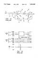
- FIG. 1Ais a block diagram of such a prior art delta-sigma modulator.
- the delta-sigma modulator 10includes a summing node 12 which sums an input signal 14 with a feedback signal on line 16.
- the summing nodeis connected to the input of an integrator 18, and the output of the integrator is filtered through a loop filter 20.
- the output of the loop filter 20is connected to the input of a quantizer or A/D convertor shown as a comparator 22.
- the output of the comparator 22forms the output, DOUT, of the modulator on line 24 and also forms the input to the switched capacitor feedback circuit shown generally as 26.
- the output of the switched capacitor feedback circuitis the feedback signal to the summing node 12.
- the switched capacitor feedback circuit 26includes a first single pole, double throw switch 28, which switches between a reference voltage, Vref, and ground in response to the output signal DOUT on line 24.
- the feedback capacitor 30, shown as C FBhas a first terminal connected to the pole of a switch 28, shown as element “a” of switch 28, and its opposite terminal connected to a node 32 which is also connected to the pole of another single pole, double throw switch 34.
- the pole of switch 34, shown as element “a” of switch 34is either connected to throw "c” which is connected to ground, or to throw "b” which is connected the summing node 12 in a timing sequence that is well known in the art and shown in FIG. 2B.
- switch 28is connected to either throw “b” which is connected to Vref, or to throw “c” which is connected to ground, depending on the state of the DOUT signal on line 24 while switch 30 is coupled to ground.
- switches 28 and 30are switched in order to provide the appropriate charge onto the summing node 12 as determined by the DOUT signal on line 24.
- the timing signals for switch 28 and the voltage signal node 32show a solid line when switch 28 is switching from the a-b to the a-c position and a dotted line when switch 28 is switching from the a-c position to the a-b position.
- the shaded area in the timing diagram for switch 28indicates that the switches may be either closed or open depending on the output of the comparator 22 on line 24.
- Shown in an illustrated embodiment of the inventionis a switched capacitor circuit in which the input signal to the capacitor is coupled to a different voltage N times during a sampling period, where N is greater than 2, and the other side of the sampling capacitor is switched between a reference voltage and an output node once during the sampling period.
- Also shown in an illustrated embodiment of the inventionis a method for transferring charge to an output terminal which includes the steps of first charging a capacitor to a first voltage by coupling a first terminal of the capacitor to a first voltage while coupling the second terminal to a reference voltage. Then coupling the second terminal to an output terminal with the first terminal coupled to the first voltage. Then coupling the first terminal to a second reference voltage while the second terminal remains coupled to the output terminal, and then coupling the first terminal to a third voltage.
- the second voltagehaving a magnitude which is between that of the first voltage and the third voltage.
- FIG. 1Ais a block diagram of a prior art delta-sigma modulator
- FIG. 1Bis a timing diagram for the switched capacitor feedback circuit shown in FIG. 1A;
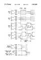
- FIG. 2Ais a block diagram of a delta-sigma modulator which includes a switched capacitor feedback circuit according to the present invention
- FIG. 2Bis a timing diagram for the switched capacitor feedback circuit shown in FIG. 2A;
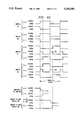
- FIG. 3Ais a block diagram of a delta-sigma modulator which includes the preferred embodiment of a switched capacitor feedback circuit according to the present invention
- FIG. 3Bis a timing diagram for the switched capacitor feedback circuit shown in FIG. 3A;
- FIG. 4Ais a schematic diagram of a differential switched capacitor integrator according to the present invention.
- FIG. 4Bis a timing diagram for the differential switched capacitor integrator shown in FIG. 4A.
- a switched capacitor feedback circuit as used in the preferred embodiment of the present inventionutilizes a three positioned switch in the input to the feedback capacitor to thereby couple plus Vref, ground, and minus Vref to charge the capacitor in two discrete steps.
- a differential referenceBy using a differential reference, and by halving the feedback capacitance, a total charge of 2 ⁇ Vref ⁇ C FB /2 is transferred in each sampling period. This is in contrast to prior art circuits which used only Vref to provide the same charge transfer of Vref ⁇ C FB .
- the inventionprovides the same signal charge by halving the feedback capacitance C FB and doubling the reference step amplitude.
- Thermal noise chargeis independent of Vref and so the invention enjoys a reduced thermal noise, Qnoise, as shown in equation 1 above. Therefore, by using the plus Vref and minus Vref, and by charging the feedback capacitor in two discrete steps, a 3 dB signal-to-noise improvement is achieved over the prior art circuit shown in FIG. 1A.
- the inventionprovides the reduced thermal noise by adding an additional switch or "detent" in the switching process.
- detentis borrowed from mechanical switch terminology. Multi-positioned mechanical rotary switches contain detents to hold a switch in each contact position.
- FIG. 2Ais block diagram of a delta-sigma modulator 36 which uses a switched capacitor feedback circuit 38 according to the present invention.
- FIG. 2Ais the same as FIG. 1A except that the switch 28 has been replaced by a three position switch 40.
- Switch 40initially begins in either position a-b or a-d (depending on the output of the comparator 22) with switch 34 initially at position a-c so that the capacitor C FB is charged to -Vref or +Vref.
- Switch 34then transitions to position a-b followed immediately by switch 40 transitioning to its position a-c. In this state a charge of C FB times Vref has been transferred to the summing node.
- the peak voltage during the charging phase which appears at node 32is +Vref of -Vref as shown in the FIG. 2B.
- the next stepis the transition of switch 40 to position a-d or a-b.
- This transitiontransfers an additional charge on C FB to the summing node and again creates a peak voltage of -Vref or +Vref on node 32.
- the capacitance of C FB of FIG. 2Ais one-half the capacitance of C FB of FIG. 1A, both circuits transfer the same amount of charge to the summing node 12.
- the circuit of FIG. 2Acan have a 3 dB improvement of Qnoise compared to FIG. 1A without degradation caused by the hot electron effect.
- a solid lineindicates the switch positions when switch 40 transitions from position a-b, through position a-c, to position a-d while the dashed line shows the switch positions when switch 40 transitions from position a-d, through position a-c, to position a-b.
- the shaded areas in the timing diagram for switch 40are regions in which switches can be either closed or open depending on the output of the comparator 22 on line 24.
- FIG. 3Ais a block diagram of a delta-sigma modulator 46 which includes the preferred embodiment of a switched capacitor feedback circuit 48 according to the present invention.
- the switched capacitor feedback circuit 38 of FIG. 2Ahas been replaced by two similar circuits 50 and 52.
- Circuit 50includes a capacitor 52 together with a three position switch 54 which places charge onto the capacitor 52 and a two position switch 56 which couples the charge from the capacitor 52 onto the summing node 12.
- Circuit 52is similar in that it includes a capacitor 58, a three position switch 60 which provides charge to the capacitor 58, and a two position switch 62 which couples the charge from the capacitor 58 onto the summing node 12.
- the switched capacitor feedback circuit 48differs from switched feedback capacitor 38 of FIG.
- switch 54switches from position a-b through position a-c to position a-d during each sampling period while position 60 switches from position a-d through a-c to position a-b during the same sampling periods.
- the two position switches 56 and 60are now controlled by the output of the comparator 22 so that one of the capacitors 52 or 58 is coupled to the summing node 12 while the other capacitor remains coupled to ground during the sampling period.
- FIG. 3AAlso shown in FIG. 3A is a transistor level schematic diagram for the two circuits 50 and 52.
- the capacitors 52 and 58have their charging terminals connected to the drain of a p-channel transistor 64 which has its source connected to +Vref.
- transistor 64forms switch position a-b.
- An n-channel transistor 66is coupled between the drain of transistor 64 and ground to form the position a-c of switches 54 and 60
- an n-channel transistor 68is coupled between the drains of transistors 64 and 66 and -Vref to form the switch position a-d of switches 54 and 60.
- another n-channel transistor, 72is coupled between the output of the capacitors 52 and 58 and ground and forms the switch positions a-c of switches 56 and 62.
- the n-channel transistors 70 and 72are placed in p wells which are biased by -Vref in the preferred embodiment.
- switch 56 and 62change position during the sampling period or remain constant depending on the output of the comparator 22 on line 24.
- one of the circuits 50 or 52will transfer charge to the summing node while the other circuit will not be connected to the summing node but will rather dump the charge to ground through switch position a-c of switches 56 or 62.
- Switches 54 and 60always operate the same during each sampling period to provide either a positive charge or a negative charge to the summing node 12.
- the timing signals shown in FIG. 3Bare the timing signals used to drive the gates of the transistors shown in FIG. 3A. More specifically, timing signals shown for position a-b of switches 56 and 62 are used as timing signals for the gate of transistor 70, the timing signals used for positions a-c of switches 56 and 62 are used as timing signals for the gate of transistor 72, the timing signals for position a-b of switches 54 and 60 are used as timing signals for the gate of transistor 64, the timing signals of switch positions a-c of switches 54 and 60 are used as the timing signals for transistor 66, and the timing signals for switch positions a-d of switches 54 and 60 are used as timing signals for the gate of transistor 68.
- switch position a-b of switches 56 and 62are first broken and then switch position a-c is closed.
- a short time later, particularly on the order of 10 nanoseconds, switch position a-b of switch 54 and switch position a-d of switch 60are open followed by the closing of switch positions a-c of switches 54 and 60.
- the width of the closure of switch position a-c of switches 54 and 60is on the order of 200 nanoseconds.
- the general theory followed in the switchingis to open the switches before the next position is closed. In other words, a "break-before-make" operation.
- the present inventioncan also be expanded to include not only three position switches but four or more position switches in order to allow the charge transfer to the summing node to be as large as possible while minimizing the size of the feedback capacitor C FB .
- the additional switch positionsrequire additional time to transfer the charge.
- the present inventioncan also be applied to differential switched capacitor integrators as shown in FIG. 4A.
- the differential switched capacitor integrator 70includes a first switched input capacitor circuit, shown generally as element 72, which receives as inputs a positive analog signal, V i+ , an input common mode voltage signal, V icm , and a negative analog signal, V i- .
- the output of the first switched capacitor circuit 72is connected to the positive input of a differential amplifier 76, and the output of the second switched capacitor circuit 74 is connected to the negative input of the differential amplifier 76.
- the negative output of the differential amplifier 76forms the positive output of the integrator, V o+ , and the positive output forms the negative output of the integrator, V o- .
- Coupled between the positive input and the negative output of the differential amplifier 76is a capacitor C 2A .
- Coupled between the negative input and the positive output of the differential amplifier 76is another capacitor C 2B .
- the switched capacitor circuit 72includes a capacitor C 1A which is selectively coupled to the three input signals V i+ , V icm , and V i- by switch 54.
- Switch 54has its pole, shown as element “a”, connected to the capacitor C 1A , its throw “b” connected to V i+ , its throw “c” connected to V icm , and its throw “d” connected to V i- .
- Connected to the other side of capacitor C 1Ais another switch 78 which has its pole, shown as element “a”, connected to the capacitor C 1A , its throw “b” connected to the positive input of the differential amplifier 76, and its throw "c” connected to a reference voltage V cm2 .
- the switched capacitor circuit 74includes a capacitor C 1B and switches 60 and 80.
- the capacitor B 1B , and switches 60 and 80are connected the same as capacitor C 1A , and switches 54 and 78 respectively except that the throw "b" of switch 80 is connected to the negative input of the differential amplifier 76 instead of the positive input.
- the input common mode voltage signal V icmis always halfway between the positive analog signal V i+ , and the negative analog signal V i- .
- V idis the differential input voltage.
- V cm2can be the same as V icm but does not have to be the same.
- V cm2could be ground while V icm could be an external signal from the analog source.
- switches 54 and 60With reference now to FIG. 4B, the operation of switches 54 and 60 is the same as shown in FIG. 3B.
- Switches 78 and 80operate the same as switches 56 and 62 of FIG. 3A except that switches 78 and 80 always switch from V cm2 to one of the inputs of the differential amplifier during each sample period. Therefore each of the switched capacitor input circuits 72 and 74 transfer both differential signals to an input of the differential amplifier 76 at two different times during each sample period. As a result the maximum voltage swing at the poles of switches 78 and 80 is only equal to one-half the analog voltage, and the hot carrier effects can be avoided.
Landscapes
- Engineering & Computer Science (AREA)
- Theoretical Computer Science (AREA)
- Compression, Expansion, Code Conversion, And Decoders (AREA)
Abstract
Description
V.sub.i+ =V.sub.icm +V.sub.id /2
V.sub.i- =V.sub.icm -V.sub.id /2
Claims (12)
Priority Applications (1)
| Application Number | Priority Date | Filing Date | Title |
|---|---|---|---|
| US07/970,693US5351050A (en) | 1992-11-03 | 1992-11-03 | Detent switching of summing node capacitors of a delta-sigma modulator |
Applications Claiming Priority (1)
| Application Number | Priority Date | Filing Date | Title |
|---|---|---|---|
| US07/970,693US5351050A (en) | 1992-11-03 | 1992-11-03 | Detent switching of summing node capacitors of a delta-sigma modulator |
Publications (1)
| Publication Number | Publication Date |
|---|---|
| US5351050Atrue US5351050A (en) | 1994-09-27 |
Family
ID=25517338
Family Applications (1)
| Application Number | Title | Priority Date | Filing Date |
|---|---|---|---|
| US07/970,693Expired - LifetimeUS5351050A (en) | 1992-11-03 | 1992-11-03 | Detent switching of summing node capacitors of a delta-sigma modulator |
Country Status (1)
| Country | Link |
|---|---|
| US (1) | US5351050A (en) |
Cited By (28)
| Publication number | Priority date | Publication date | Assignee | Title |
|---|---|---|---|---|
| US5644257A (en)* | 1993-03-24 | 1997-07-01 | Crystal Semiconductor Corporation | Sampling circuit charge management |
| US5719572A (en)* | 1994-07-08 | 1998-02-17 | Cirrus Logic, Inc. | Digital signal processor with reduced pattern dependent noise |
| US5801652A (en)* | 1994-07-08 | 1998-09-01 | Cirrus Logic, Inc. | Pattern dependent noise reduction in a digital processing circuit utilizing image circuitry |
| US5841310A (en)* | 1997-04-08 | 1998-11-24 | Burr-Brown Corporation | Current-to-voltage integrator for analog-to-digital converter, and method |
| US5872532A (en)* | 1994-09-30 | 1999-02-16 | Kabushiki Kaisha Toshiba | Selection apparatus |
| US5959565A (en)* | 1996-11-29 | 1999-09-28 | Rohm Co., Ltd. | Switched capacitor |
| EP0982863A1 (en)* | 1998-08-28 | 2000-03-01 | Texas Instruments Incorporated | Switched capacitor comparator and D/A converter |
| US6172630B1 (en)* | 1998-08-18 | 2001-01-09 | Tektronix, Inc. | Extended common mode input range for a delta-sigma converter |
| US6396428B1 (en) | 2001-06-04 | 2002-05-28 | Raytheon Company | Continuous time bandpass delta sigma modulator ADC architecture with feedforward signal compensation |
| US6614285B2 (en)* | 1998-04-03 | 2003-09-02 | Cirrus Logic, Inc. | Switched capacitor integrator having very low power and low distortion and noise |
| US6727749B1 (en)* | 2002-08-29 | 2004-04-27 | Xilinx, Inc. | Switched capacitor summing system and method |
| US6816100B1 (en) | 1999-03-12 | 2004-11-09 | The Regents Of The University Of California | Analog-to-digital converters with common-mode rejection dynamic element matching, including as used in delta-sigma modulators |
| US20050174274A1 (en)* | 2004-02-05 | 2005-08-11 | Brad Delanghe | Method and system for mixed analog-digital automatic gain control |
| US20050237694A1 (en)* | 2004-04-21 | 2005-10-27 | Analog Devices, Inc. | Methods and apparatus for reducing thermal noise |
| US20060119412A1 (en)* | 2004-12-03 | 2006-06-08 | Silicon Laboratories, Inc. | Switched capacitor input circuit and method therefor |
| US20060119411A1 (en)* | 2004-12-03 | 2006-06-08 | Silicon Laboratories, Inc. | Switched capacitor sampler circuit and method therefor |
| US20070179897A1 (en)* | 2006-01-27 | 2007-08-02 | Stefan Andersson | Conditional stream access |
| US7324029B2 (en)* | 2006-01-26 | 2008-01-29 | Emerson Process Management | Capacitance-to-digital interface circuit for differential pressure sensor |
| US20090051429A1 (en)* | 2007-08-22 | 2009-02-26 | Shen David H | High resolution variable gain control |
| US20090195423A1 (en)* | 2008-02-06 | 2009-08-06 | O2Micro, Inc. | Analog to digital converters |
| EP2088677A1 (en) | 2008-02-06 | 2009-08-12 | O2Micro, Inc. | Analog to digital converters |
| US20090278720A1 (en)* | 2008-05-07 | 2009-11-12 | Schneider Edmund M | Delta-sigma analog-to-digital converter circuit having reduced sampled reference noise |
| US20100328122A1 (en)* | 2008-02-06 | 2010-12-30 | Guoxing Li | Analog to digital converters |
| US8009077B1 (en) | 2009-06-08 | 2011-08-30 | Cirrus Logic, Inc. | Delta-sigma analog-to-digital converter (ADC) circuit with selectively switched reference |
| US20120274363A1 (en)* | 2011-04-28 | 2012-11-01 | Analog Devices, Inc. | Noise cancellation system and method for amplifiers |
| WO2013039607A1 (en)* | 2011-09-15 | 2013-03-21 | Analog Devices, Inc. | Apparatus and methods for adaptive common mode level shifting |
| US8432222B2 (en) | 2011-09-15 | 2013-04-30 | Analog Devices, Inc. | Apparatus and methods for electronic amplification |
| CN110313133A (en)* | 2017-02-15 | 2019-10-08 | 株式会社电装 | Deltasigma modulator, Δ Σ A/D converter and increment Delta Σ A/D converter |
Citations (3)
| Publication number | Priority date | Publication date | Assignee | Title |
|---|---|---|---|---|
| US4851841A (en)* | 1987-10-02 | 1989-07-25 | Crystal Semiconductor Corporation | Gain scaling of oversampled analog-to-digital converters |
| US5099195A (en)* | 1989-12-18 | 1992-03-24 | The General Electric Company, P.L.C. | Electronic device for measuring electrical power supply to a load |
| US5148167A (en)* | 1990-04-06 | 1992-09-15 | General Electric Company | Sigma-delta oversampled analog-to-digital converter network with chopper stabilization |
- 1992
- 1992-11-03USUS07/970,693patent/US5351050A/ennot_activeExpired - Lifetime
Patent Citations (3)
| Publication number | Priority date | Publication date | Assignee | Title |
|---|---|---|---|---|
| US4851841A (en)* | 1987-10-02 | 1989-07-25 | Crystal Semiconductor Corporation | Gain scaling of oversampled analog-to-digital converters |
| US5099195A (en)* | 1989-12-18 | 1992-03-24 | The General Electric Company, P.L.C. | Electronic device for measuring electrical power supply to a load |
| US5148167A (en)* | 1990-04-06 | 1992-09-15 | General Electric Company | Sigma-delta oversampled analog-to-digital converter network with chopper stabilization |
Cited By (46)
| Publication number | Priority date | Publication date | Assignee | Title |
|---|---|---|---|---|
| US5644257A (en)* | 1993-03-24 | 1997-07-01 | Crystal Semiconductor Corporation | Sampling circuit charge management |
| US5719572A (en)* | 1994-07-08 | 1998-02-17 | Cirrus Logic, Inc. | Digital signal processor with reduced pattern dependent noise |
| US5801652A (en)* | 1994-07-08 | 1998-09-01 | Cirrus Logic, Inc. | Pattern dependent noise reduction in a digital processing circuit utilizing image circuitry |
| US5872532A (en)* | 1994-09-30 | 1999-02-16 | Kabushiki Kaisha Toshiba | Selection apparatus |
| US5959565A (en)* | 1996-11-29 | 1999-09-28 | Rohm Co., Ltd. | Switched capacitor |
| US5841310A (en)* | 1997-04-08 | 1998-11-24 | Burr-Brown Corporation | Current-to-voltage integrator for analog-to-digital converter, and method |
| US6614285B2 (en)* | 1998-04-03 | 2003-09-02 | Cirrus Logic, Inc. | Switched capacitor integrator having very low power and low distortion and noise |
| DE19938045C2 (en)* | 1998-08-18 | 2003-03-27 | Tektronix Inc | Extended common-mode input range for a delta-sigma modulator |
| US6172630B1 (en)* | 1998-08-18 | 2001-01-09 | Tektronix, Inc. | Extended common mode input range for a delta-sigma converter |
| EP0982863A1 (en)* | 1998-08-28 | 2000-03-01 | Texas Instruments Incorporated | Switched capacitor comparator and D/A converter |
| US6249240B1 (en) | 1998-08-28 | 2001-06-19 | Texas Instruments Incorporated | Switched-capacitor circuitry with reduced loading upon reference voltages |
| US6816100B1 (en) | 1999-03-12 | 2004-11-09 | The Regents Of The University Of California | Analog-to-digital converters with common-mode rejection dynamic element matching, including as used in delta-sigma modulators |
| US6396428B1 (en) | 2001-06-04 | 2002-05-28 | Raytheon Company | Continuous time bandpass delta sigma modulator ADC architecture with feedforward signal compensation |
| US6727749B1 (en)* | 2002-08-29 | 2004-04-27 | Xilinx, Inc. | Switched capacitor summing system and method |
| US20050174274A1 (en)* | 2004-02-05 | 2005-08-11 | Brad Delanghe | Method and system for mixed analog-digital automatic gain control |
| US7218258B2 (en)* | 2004-02-05 | 2007-05-15 | Broadcom Corporation | Method and system for mixed analog-digital automatic gain control |
| US20050237694A1 (en)* | 2004-04-21 | 2005-10-27 | Analog Devices, Inc. | Methods and apparatus for reducing thermal noise |
| WO2005107077A1 (en) | 2004-04-21 | 2005-11-10 | Analog Devices, Inc. | Methods and apparatus for reducing thermal noise |
| US7298151B2 (en) | 2004-04-21 | 2007-11-20 | Analog Devices, Inc. | Methods and apparatus for reducing thermal noise |
| US20060119412A1 (en)* | 2004-12-03 | 2006-06-08 | Silicon Laboratories, Inc. | Switched capacitor input circuit and method therefor |
| US20060119411A1 (en)* | 2004-12-03 | 2006-06-08 | Silicon Laboratories, Inc. | Switched capacitor sampler circuit and method therefor |
| US7157956B2 (en) | 2004-12-03 | 2007-01-02 | Silicon Laboratories, Inc. | Switched capacitor input circuit and method therefor |
| US7157955B2 (en) | 2004-12-03 | 2007-01-02 | Silicon Laboratories, Inc. | Switched capacitor sampler circuit and method therefor |
| US7324029B2 (en)* | 2006-01-26 | 2008-01-29 | Emerson Process Management | Capacitance-to-digital interface circuit for differential pressure sensor |
| US20070179897A1 (en)* | 2006-01-27 | 2007-08-02 | Stefan Andersson | Conditional stream access |
| US20090051429A1 (en)* | 2007-08-22 | 2009-02-26 | Shen David H | High resolution variable gain control |
| US7982539B2 (en) | 2007-08-22 | 2011-07-19 | Nanoamp Mobile, Inc. | High resolution variable gain control |
| US20090195423A1 (en)* | 2008-02-06 | 2009-08-06 | O2Micro, Inc. | Analog to digital converters |
| EP2088677A1 (en) | 2008-02-06 | 2009-08-12 | O2Micro, Inc. | Analog to digital converters |
| US7796069B2 (en) | 2008-02-06 | 2010-09-14 | 02Micro International Limited | Analog to digital converters |
| US20100328122A1 (en)* | 2008-02-06 | 2010-12-30 | Guoxing Li | Analog to digital converters |
| US8193959B2 (en) | 2008-02-06 | 2012-06-05 | O2Micro, Inc. | Analog to digital converters |
| US20090278720A1 (en)* | 2008-05-07 | 2009-11-12 | Schneider Edmund M | Delta-sigma analog-to-digital converter circuit having reduced sampled reference noise |
| US7746257B2 (en) | 2008-05-07 | 2010-06-29 | Cirrus Logic, Inc. | Delta-sigma analog-to-digital converter circuit having reduced sampled reference noise |
| US8009077B1 (en) | 2009-06-08 | 2011-08-30 | Cirrus Logic, Inc. | Delta-sigma analog-to-digital converter (ADC) circuit with selectively switched reference |
| US20120274363A1 (en)* | 2011-04-28 | 2012-11-01 | Analog Devices, Inc. | Noise cancellation system and method for amplifiers |
| US8508257B2 (en)* | 2011-04-28 | 2013-08-13 | Analog Devices, Inc. | Noise cancellation system and method for amplifiers |
| CN103493138A (en)* | 2011-04-28 | 2014-01-01 | 美国亚德诺半导体公司 | Noise cancellation system and method for amplifiers |
| CN103493138B (en)* | 2011-04-28 | 2016-08-24 | 美国亚德诺半导体公司 | Noise canceling system and method for amplifier |
| WO2013039607A1 (en)* | 2011-09-15 | 2013-03-21 | Analog Devices, Inc. | Apparatus and methods for adaptive common mode level shifting |
| US8432222B2 (en) | 2011-09-15 | 2013-04-30 | Analog Devices, Inc. | Apparatus and methods for electronic amplification |
| US8552788B2 (en)* | 2011-09-15 | 2013-10-08 | Analog Devices, Inc. | Apparatus and methods for adaptive common-mode level shifting |
| CN103797711A (en)* | 2011-09-15 | 2014-05-14 | 美国亚德诺半导体公司 | Apparatus and methods for adaptive common mode level shifting |
| CN103797711B (en)* | 2011-09-15 | 2016-09-28 | 美国亚德诺半导体公司 | Equipment and method for the conversion of self adaptation common mode electrical level |
| DE112012003868B4 (en)* | 2011-09-15 | 2017-10-19 | Analog Devices, Inc. | Apparatus and method for adaptive common mode shift |
| CN110313133A (en)* | 2017-02-15 | 2019-10-08 | 株式会社电装 | Deltasigma modulator, Δ Σ A/D converter and increment Delta Σ A/D converter |
Similar Documents
| Publication | Publication Date | Title |
|---|---|---|
| US5351050A (en) | Detent switching of summing node capacitors of a delta-sigma modulator | |
| US4365204A (en) | Offset compensation for switched capacitor integrators | |
| Fiez et al. | Switched-current circuit design issues | |
| US4543534A (en) | Offset compensated switched capacitor circuits | |
| US5644257A (en) | Sampling circuit charge management | |
| US4570084A (en) | Clocked differential cascode voltage switch logic systems | |
| US5187390A (en) | Input sampling switch charge conservation | |
| JPS6244597Y2 (en) | ||
| KR100509714B1 (en) | Low Noise, Low Power CMOS Correlated Double Sampler | |
| KR0175299B1 (en) | Comparator circuitry | |
| US4866368A (en) | Circuit arrangement for storing sampled analogue electrical currents | |
| CA1173118A (en) | Intergrator with sampling stage | |
| US20020113724A1 (en) | Code independent charge transfer scheme for switched-capacitor digital-to-analog converter | |
| WO2003105348A1 (en) | Delta - sigma modulators with improved noise performance | |
| US5977895A (en) | Waveform shaping circuit for function circuit and high order delta sigma modulator | |
| US4746871A (en) | Differential switched capacitor integrator using a single integration capacitor | |
| US20020021162A1 (en) | Boosted switch device for a sampler of an analog/digital converter, and operating method thereof | |
| US20050017793A1 (en) | Boosted sampling circuit and relative method of driving | |
| GB1562774A (en) | Circuits for generating sequences of signals | |
| US4716319A (en) | Switched capacitor filter for low voltage applications | |
| GB2317726A (en) | Multiplier and neural network synapse using current mirrors having low-power MOSFETs | |
| US4837527A (en) | Switched capacitor arrangement | |
| RU2144213C1 (en) | Integration circuit with frequency modulation | |
| Albarran et al. | A charge-transfer multiplying digital-to-analog converter | |
| CA1262476A (en) | A modified cascode amplifier |
Legal Events
| Date | Code | Title | Description |
|---|---|---|---|
| AS | Assignment | Owner name:CRYSTAL SEMICONDUCTOR CORP., TEXAS Free format text:ASSIGNMENT OF ASSIGNORS INTEREST.;ASSIGNORS:THOMPSON, CHARLES D.;SWANSON, ERIC J.;REEL/FRAME:006417/0942 Effective date:19921030 | |
| FEPP | Fee payment procedure | Free format text:PAYOR NUMBER ASSIGNED (ORIGINAL EVENT CODE: ASPN); ENTITY STATUS OF PATENT OWNER: LARGE ENTITY | |
| STCF | Information on status: patent grant | Free format text:PATENTED CASE | |
| AS | Assignment | Owner name:BANK OF AMERICA NATIONAL TRUST & SAVINGS ASSOCIATI Free format text:SECURITY INTEREST;ASSIGNOR:CRYSTAL SEMICONDUCTOR CORPORATION;REEL/FRAME:007986/0878 Effective date:19960430 | |
| FPAY | Fee payment | Year of fee payment:4 | |
| AS | Assignment | Owner name:CIRRUS LOGIC, INC., TEXAS Free format text:ASSIGNMENT OF ASSIGNORS INTEREST;ASSIGNOR:CRYSTAL SEMICONDUCTOR CORPORATION;REEL/FRAME:010742/0623 Effective date:20000322 | |
| FEPP | Fee payment procedure | Free format text:PAYER NUMBER DE-ASSIGNED (ORIGINAL EVENT CODE: RMPN); ENTITY STATUS OF PATENT OWNER: LARGE ENTITY Free format text:PAYOR NUMBER ASSIGNED (ORIGINAL EVENT CODE: ASPN); ENTITY STATUS OF PATENT OWNER: LARGE ENTITY | |
| FPAY | Fee payment | Year of fee payment:8 | |
| REMI | Maintenance fee reminder mailed | ||
| FPAY | Fee payment | Year of fee payment:12 |