US5347258A - Annular resistor coupled with printed circuit board through-hole - Google Patents
Annular resistor coupled with printed circuit board through-holeDownload PDFInfo
- Publication number
- US5347258A US5347258AUS08/044,301US4430193AUS5347258AUS 5347258 AUS5347258 AUS 5347258AUS 4430193 AUS4430193 AUS 4430193AUS 5347258 AUS5347258 AUS 5347258A
- Authority
- US
- United States
- Prior art keywords
- resistor
- conductive
- resistor body
- conductive layer
- hole
- Prior art date
- Legal status (The legal status is an assumption and is not a legal conclusion. Google has not performed a legal analysis and makes no representation as to the accuracy of the status listed.)
- Expired - Lifetime
Links
Images


Classifications
- H—ELECTRICITY
- H05—ELECTRIC TECHNIQUES NOT OTHERWISE PROVIDED FOR
- H05K—PRINTED CIRCUITS; CASINGS OR CONSTRUCTIONAL DETAILS OF ELECTRIC APPARATUS; MANUFACTURE OF ASSEMBLAGES OF ELECTRICAL COMPONENTS
- H05K1/00—Printed circuits
- H05K1/16—Printed circuits incorporating printed electric components, e.g. printed resistor, capacitor, inductor
- H05K1/167—Printed circuits incorporating printed electric components, e.g. printed resistor, capacitor, inductor incorporating printed resistors
- H—ELECTRICITY
- H05—ELECTRIC TECHNIQUES NOT OTHERWISE PROVIDED FOR
- H05K—PRINTED CIRCUITS; CASINGS OR CONSTRUCTIONAL DETAILS OF ELECTRIC APPARATUS; MANUFACTURE OF ASSEMBLAGES OF ELECTRICAL COMPONENTS
- H05K1/00—Printed circuits
- H05K1/16—Printed circuits incorporating printed electric components, e.g. printed resistor, capacitor, inductor
- H05K1/162—Printed circuits incorporating printed electric components, e.g. printed resistor, capacitor, inductor incorporating printed capacitors
- H—ELECTRICITY
- H05—ELECTRIC TECHNIQUES NOT OTHERWISE PROVIDED FOR
- H05K—PRINTED CIRCUITS; CASINGS OR CONSTRUCTIONAL DETAILS OF ELECTRIC APPARATUS; MANUFACTURE OF ASSEMBLAGES OF ELECTRICAL COMPONENTS
- H05K1/00—Printed circuits
- H05K1/16—Printed circuits incorporating printed electric components, e.g. printed resistor, capacitor, inductor
- H05K1/165—Printed circuits incorporating printed electric components, e.g. printed resistor, capacitor, inductor incorporating printed inductors
- H—ELECTRICITY
- H05—ELECTRIC TECHNIQUES NOT OTHERWISE PROVIDED FOR
- H05K—PRINTED CIRCUITS; CASINGS OR CONSTRUCTIONAL DETAILS OF ELECTRIC APPARATUS; MANUFACTURE OF ASSEMBLAGES OF ELECTRICAL COMPONENTS
- H05K1/00—Printed circuits
- H05K1/02—Details
- H05K1/0296—Conductive pattern lay-out details not covered by sub groups H05K1/02 - H05K1/0295
- H05K1/0298—Multilayer circuits
- H—ELECTRICITY
- H05—ELECTRIC TECHNIQUES NOT OTHERWISE PROVIDED FOR
- H05K—PRINTED CIRCUITS; CASINGS OR CONSTRUCTIONAL DETAILS OF ELECTRIC APPARATUS; MANUFACTURE OF ASSEMBLAGES OF ELECTRICAL COMPONENTS
- H05K1/00—Printed circuits
- H05K1/02—Details
- H05K1/11—Printed elements for providing electric connections to or between printed circuits
- H05K1/115—Via connections; Lands around holes or via connections
- H05K1/116—Lands, clearance holes or other lay-out details concerning the surrounding of a via
- H—ELECTRICITY
- H05—ELECTRIC TECHNIQUES NOT OTHERWISE PROVIDED FOR
- H05K—PRINTED CIRCUITS; CASINGS OR CONSTRUCTIONAL DETAILS OF ELECTRIC APPARATUS; MANUFACTURE OF ASSEMBLAGES OF ELECTRICAL COMPONENTS
- H05K2201/00—Indexing scheme relating to printed circuits covered by H05K1/00
- H05K2201/08—Magnetic details
- H05K2201/083—Magnetic materials
- H05K2201/086—Magnetic materials for inductive purposes, e.g. printed inductor with ferrite core
- H—ELECTRICITY
- H05—ELECTRIC TECHNIQUES NOT OTHERWISE PROVIDED FOR
- H05K—PRINTED CIRCUITS; CASINGS OR CONSTRUCTIONAL DETAILS OF ELECTRIC APPARATUS; MANUFACTURE OF ASSEMBLAGES OF ELECTRICAL COMPONENTS
- H05K2201/00—Indexing scheme relating to printed circuits covered by H05K1/00
- H05K2201/09—Shape and layout
- H05K2201/09209—Shape and layout details of conductors
- H05K2201/0929—Conductive planes
- H05K2201/093—Layout of power planes, ground planes or power supply conductors, e.g. having special clearance holes therein
- H—ELECTRICITY
- H05—ELECTRIC TECHNIQUES NOT OTHERWISE PROVIDED FOR
- H05K—PRINTED CIRCUITS; CASINGS OR CONSTRUCTIONAL DETAILS OF ELECTRIC APPARATUS; MANUFACTURE OF ASSEMBLAGES OF ELECTRICAL COMPONENTS
- H05K2201/00—Indexing scheme relating to printed circuits covered by H05K1/00
- H05K2201/09—Shape and layout
- H05K2201/09209—Shape and layout details of conductors
- H05K2201/0929—Conductive planes
- H05K2201/09309—Core having two or more power planes; Capacitive laminate of two power planes
- H—ELECTRICITY
- H05—ELECTRIC TECHNIQUES NOT OTHERWISE PROVIDED FOR
- H05K—PRINTED CIRCUITS; CASINGS OR CONSTRUCTIONAL DETAILS OF ELECTRIC APPARATUS; MANUFACTURE OF ASSEMBLAGES OF ELECTRICAL COMPONENTS
- H05K2201/00—Indexing scheme relating to printed circuits covered by H05K1/00
- H05K2201/09—Shape and layout
- H05K2201/09209—Shape and layout details of conductors
- H05K2201/09654—Shape and layout details of conductors covering at least two types of conductors provided for in H05K2201/09218 - H05K2201/095
- H05K2201/09809—Coaxial layout
- H—ELECTRICITY
- H05—ELECTRIC TECHNIQUES NOT OTHERWISE PROVIDED FOR
- H05K—PRINTED CIRCUITS; CASINGS OR CONSTRUCTIONAL DETAILS OF ELECTRIC APPARATUS; MANUFACTURE OF ASSEMBLAGES OF ELECTRICAL COMPONENTS
- H05K2203/00—Indexing scheme relating to apparatus or processes for manufacturing printed circuits covered by H05K3/00
- H05K2203/05—Patterning and lithography; Masks; Details of resist
- H05K2203/0502—Patterning and lithography
- H05K2203/0545—Pattern for applying drops or paste; Applying a pattern made of drops or paste
- H—ELECTRICITY
- H05—ELECTRIC TECHNIQUES NOT OTHERWISE PROVIDED FOR
- H05K—PRINTED CIRCUITS; CASINGS OR CONSTRUCTIONAL DETAILS OF ELECTRIC APPARATUS; MANUFACTURE OF ASSEMBLAGES OF ELECTRICAL COMPONENTS
- H05K3/00—Apparatus or processes for manufacturing printed circuits
- H05K3/40—Forming printed elements for providing electric connections to or between printed circuits
- H05K3/42—Plated through-holes or plated via connections
- H05K3/429—Plated through-holes specially for multilayer circuits, e.g. having connections to inner circuit layers
Definitions
- the present inventionrelates to printed circuit boards and more particularly to printed circuit boards including various devices or components to be coupled with individual resistors.
- the present inventionis directed toward printed circuit boards (PCBs) and the like.
- PCBsprinted circuit boards
- These circuit boardstypically include large numbers of electronic devices which are commonly surface mounted and also additional components which may be present in the form of active layers within each PCB.
- the requirements for the devices and components in such printed circuit boardsare subject to conventional electronic design restraints.
- resistorshas increased the complexity of the PCBs and at the same time either decreased the available surface area of the PCBs for other devices or else resulted in an overall increase in the size of the PCBs to accommodate necessary surface devices and components including resistors.
- This conceptinvolved the replacement of surface mounted or discrete resistors by resistors formed on layers arranged either on or within the PCBs.
- planar resistorsprovide advantages in certain applications over discrete surface mounted resistors, they have still tended to result in relative increases in the complexity and space demands on the PCBs.
- the planar resistorsare formed on a surface layer of the PCB, it is of course possible to arrange an active surface device over the resistor.
- that surface portion of the PCB occupied by the planar resistormust be dedicated to the planar resistor itself. Accordingly, that portion of the board is not available for mounting pads, through-holes or the like.
- plated through-holeshave commonly been employed for this purpose and further increase complexity and space demands in the PCBs.
- Planar resistors of the type described abovehave also been formed on internal layers or planes of the PCBs. Such a configuration permits the use of standard subtractive PCB techniques, for example, to produce conductor patterns and resistor elements suited for high speed and high density circuit applications. However, even with the planar resistors being formed on internal layers of the PCBs, it is still necessary to provide plated through-holes or other conductors extending in a Z direction through the PCBs in order to provide the necessary couplings for the planar resistors with various surface mounted devices or components in the PCBs.
- the resistor elementsbe formed from generally conventional materials exhibiting either selected resistivity or conductivity. Accordingly, the resistance of each resistor element of the present invention is determined by its dimensions and the resistivity of the material from which it is formed.
- through-holeis employed in the present invention to refer to any Z directional conductor formed in the PCB for interconnecting a surface device or PCB component with a conductive layer on or in the PCB.
- through-holesare commonly employed for interconnecting surface devices mounted on either surface of the PCB either with an internal conductive layer or plane within the PCB or even a conductive layer on the surface of the PCB. In the latter case, the most common arrangement would be a through-hole interconnecting a surface device on one side of the PCB with a conductive layer or plane on the opposite surface of the PCB.
- through-holes of the type defined aboveare also employed for interconnecting surface mounted devices or components arranged on or in the PCB similarly with conductive layers or planes formed either on or in the PCB. Accordingly, the present invention specifically contemplates formation of its resistor elements in combination with any through-hole of the type defined above.
- a resistor assemblyin a PCB, the assembly including a conductive through-hole formed in the PCB for interconnection with a surface device or other PCB component, a conductive pad surrounding and conductively interconnected with the plated through-hole, a conductive layer surrounding and generally coplanar with the conductive pad and spaced apart from the conductive pad to form an annular recess, a resistor assembly being arranged in the annular recess and formed from a conductive material having a selected resistivity and outer and inner perimeters respectively conductively interconnected with the conductive layer and the conductive pad whereby the resistor assembly is electrically coupled along with the plated through-hole between the conductive layer and the surface device or component.
- the present inventioncontemplates such a resistor assembly or resistor assembly wherein the annular recess forms a continuous channel or separation between the conductive layer and the conductive pad or plated through-hole.
- the resistor assemblyis arranged in the annular recess and is preferably at least co-extensive with the annular recess. In such a co-extensive arrangement, the resistor assembly either extends just between the outer and inner perimeters or may even overlap the outer and inner perimeters are described in greater detail below.
- the resistor assemblymay readily be formed, for example, by deposition of a liquid precursor or by other methods of formation which will be apparent from the following description.
- the outer and inner perimeters of the resistor assemblyare preferably formed with substantially constant radii and the resistor is generally continuous between its outer and inner perimeters so that the operative resistance of the resistor assembly may be simply determined from the radii of its outer and inner perimeters, an effective thickness of the resistor assembly and its resistivity.
- the operative resistance of the resistor assembly or resistor assemblybe capable of calculation in the manner summarized above. More specifically, a typical and preferred method for calculating the operative resistance of the resistor assembly or resistor assembly is set forth immediately below.
- the effective resistance of the resistor or resistor assemblymay be determined as follows, having reference to FIG. 5B.
- Rresistance in ohms
- presistivity of the resistor in ohms centimeters
- Lthe length of the resistor in centimeters
- wthe width of the resistor in centimeters
- Hthe height of the resistor in centimeters (wH thus being the effective cross-sectional area of the resistor for purposes of calculating its resistance).
- the resistor body 62is graphically illustrated with substantially constant radii forming its outer and inner peripheries 56 and 58. Further, since the resistor body 62 forms a resistor between the conductive pad 60 and the conductive layer or upper surface 18, then the effective length of the resistor body 62 is equal to the radial dimension of the resistor body, that is r 2 -r 1 .
- the effective width of the resistor bodyis thus the mean circumference of the resistor body, that is the circumference of the resistor body generated from a point mid-way between the outer and inner peripheries 56 and 58.
- the effective width of the resistor bodymay be stated as follows: ##EQU2##
- the order in which the steps are performedmay be changed.
- the through-holecould be formed prior to deposition of the resistor assembly in the annular recess.
- a conductive padcould also be formed about the plated through-hole for interconnection with the resistor assembly.
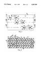
- FIG. 1is a plan view of a printed circuit board (PCB) with surface devices schematically illustrated for interconnection with various components of the PCB by respective through-holes.
- PCBprinted circuit board
- FIGS. 2, 3 and 4are respectively view taken in section along section lines II--II, III--III and IV--IV of FIG. 1.
- FIG. 5Ais a plan view of a capacitive laminate formed as a subassembly for inclusion in the PCB of FIG. 1 and illustrating, in greater detail, a resistor assembly formed according to the invention.
- FIG. 5Bis a fragmentary view of a single resistor body constructed according to the present invention and having a preferred configuration as also illustrated in FIG. 5A.
- FIG. 6is a fragmentary view taken along section lines VI--VI of FIG. 5A.
- FIG. 7is a fragmentary view illustrating a portion of a capacitive laminate similar to that illustrated in FIG. 5A to demonstrate another embodiment of the invention.
- a printed circuit boardis generally indicated at 10 conventionally formed with multiple layers as described in greater detail below with reference to FIGS. 2-4.
- Surface mounted devices 12, 14 and 16are arranged upon an upper surface 18 of the PCB for interconnection with conductive layers within the PCB as described in greater detail below.
- the internal layers of the PCBinclude a capacitive laminate 20 formed from conductive foils or layers 22 and 24 arranged on opposite sides of a dielectric layer 26 formed for example form epoxy or from other materials having a higher dielectric constant.
- the conductive foil 22is a power plane for the PCB 10 while the other conductive foil 24 is preferably a ground plane for the PCB.
- Such a higher dielectric constantcould be provided for example by a layer of epoxy or other polymer filled with a material such as any of a variety of well known ceramics (not otherwise shown).
- the PCBalso includes another conductive layer or signal plane 28 and additional layers 30, 32 and 34 arranged on opposite sides of both the capacitive laminate 20 and the signal plane 28 to complete the PCB.
- the PCB 10is described only for purposes of example.
- the inventioncontemplates any of a variety of PCBs having any number of layers.
- the inventionalso contemplates other devices or components in addition to the surface mounted devices 12, 14 and 16 which could be similarly interconnected with resistor bodies according to the present invention as described in greater detail below.
- the surface devices 12, 14 and 16are respectively interconnected with resistor assemblies 36A, 36B and 36C.
- the resistor assembliesare similarly configured but arranged in different conductive layers or planes of the PCB 10 as described in greater detail below.
- the surface mounted device 12is mounted on the surface 18 of the PCB 10 for example by mounting pads 38 and 40 which are respectively interconnected with signal traces 42 and 44.
- the signal traces 42 and 44are respectively interconnected with additional pads 46 and 48 respectively interconnected with plated through-holes 50 and 52.
- the resistor assembly 36Asurrounds and is conductively interconnected with the through-hole 50 while also being interconnected with the conductive or ground plane 24 of the capacitive laminate 20.
- the other plated through-hole 52can be interconnected with any portion or component of the PCB 10 depending upon the desired operation for the surface mounted device 12. Similar through-hole interconnections are provided for the surface mounted devices 14 and 16. Accordingly, the corresponding components of the surface mounting connections for those devices are indicated respectively by primed numerals and double-primed numerals otherwise corresponding to the through-hole connections described above for the surface mounted device 12.
- the resistor assembly 36Bis similarly constructed as the resistor assembly 36A illustrated in FIG. 2 but is interconnected with the conductive foil or power plane 22.
- the resistor assembly 36Cis also similarly constructed as the resistor assembly 36A while being arranged in conductive relation with the additional signal plane 28.
- a resistor assembly constructed according to the present inventionmay be arranged at the intersection of any through-hole with any conductive plane or layer (or combination thereof) in a PCB or the like
- FIGS. 2 and 3specifically illustrate resistor assemblies interconnected with either the power or ground planes 22 and 24 of a capacitive laminate. It will further be apparent from FIGS. 2 and 3 in combination with FIG. 1 that the surface devices 12 and 14 could thus be interconnected with both the respective resistor assemblies as well as the capacitive laminate by means of the same respective through-holes.
- FIG. 4illustrates that the resistor assembly could be arranged in other conductive layers of the PCB. It is also to be understood that those conductive layers could even be formed on one of the lateral surfaces of the PCB.
- the resistor assemblies 36A, 36B and 36C of FIGS. 2-4are generally illustrated at the intersection of through-holes formed in the PCB 10 for other purposes. More specifically, the through-holes illustrated in FIGS. 2-4 are generally contemplated for providing necessary electrical connections for the respective surface devices with various components within the PCB. In that case, the resistor assemblies 36A, 36B and 36C are merely added at the juncture of those pre-existing through-holes with selected conductive layers in the PCB.
- a resistor assembly constructed according to the present inventioncould similarly be provided at the intersection of a through-hole and a conductive plane, such a through-hole specifically being provided for purposes of connection with the resistor assembly.
- the resistor assembly of the present inventionis not to be limited to use with through-holes pre-existing in the PCB for other purposes.
- resistor assembly 36AThe construction of the resistor assembly 36A is illustrated in greater detail in FIGS. 5A and 6. Here again, it is to be understood that the configuration of the resistor assemblies 36B and 36C is similar to that described below for resistor assembly 36A.
- the capacitive laminate 20is illustrated as a component for inclusion in the PCB 10 of FIGS. 1-4.
- the conductive foils or power and ground planes 22 and 24are initially laminated to the dielectric layer 26 in order to form the capacitive laminate 20 as a structurally self-supporting component.
- the resistor assembly 36Ais formed on the upper conductive foil or power plane 22.
- the method of formation for the resistor assemblyis particularly simple.
- the method of formation for the resistor assembly of the inventionmakes it particularly easy to change the effective resistance for each resistor assembly as described in greater detail below.
- annular recess 54is formed in the conductive foils or power plane 22 between an outer periphery 56 and an inner periphery 58.
- formation of the annular recess 54also forms a conductive pad 60 between the inner periphery 58 and the plated through-hole 50.
- the power plane 22is formed from conductive material, it is thus a simple matter to etch the annular recess 54 at the same time that other circuit elements are etched into the conductive foil 22 as is conventional for a capacitive laminate in such a PCB.
- a resistor body 62is then arranged or formed in the annular recess 54 so that it is electrically interconnected with the power plane 22 and the conductive pad 60 at the outer and inner peripheries 56 and 58 respectively.
- the annular recess 54is formed with its outer and inner peripheries 56 and 58 having constant radii and the conductive pad 60 having a similar thickness as the power plane 22, at least adjacent the inner and outer peripheries 58 and 56.
- FIG. 5Bis provided to illustrate a simplified manner of calculation for determining the resistance of the resistor body 62 as described in greater detail below.
- the effective resistance of the resistor or resistor assemblymay be determined as follows, having reference to FIG. 5B.
- Rresistance in ohms
- presistivity of the resistor in ohms centimeters
- Lthe length of the resistor in centimeters
- wthe width of the resistor in centimeters
- Hthe height of the resistor in centimeters (wH thus being the effective cross-sectional area of the resistor for purposes of calculating its resistance).
- the resistor body 62is graphically illustrated with substantially constant radii forming its outer and inner peripheries 56 and 58. Further, since the resistor body 62 forms a resistor between the conductive pad 60 and the conductive layer or upper surface 18, then the effective length of the resistor body 62 is equal to the radial dimension of the resistor body, that is r 2 -r 1 .
- the effective width of the resistor bodyis thus the mean circumference of the resistor body, that is the circumference of the resistor body generated from a point mid-way between the outer and inner peripheries 56 and 58.
- the effective width of the resistor bodymay be stated as follows: ##EQU4##
- its effective resistancemay be predetermined simply by selecting the appropriate radii for the outer and inner peripheries 56 and 58.
- the radii for the peripheries of the resistor bodycould then be selected in order to establish its effective resistance.
- the resistor bodyis preferably formed from a liquid precursor such as a powdered resistor material suspended in a liquid. In this manner, the resistor body could be deposited and formed by conventional techniques if necessary or desired. However, it is to be understood that the resistor body could also be formed from other precursors either in liquid or paste or of other consistencies, even a dry film, for example.
- any liquid precursormay be employed for forming the resistor body as long as the precursor is capable of being filled or otherwise combined with a suitable resistor material either in the form of a powder or possibly larger particles.
- the precursormust also be selected so that it is capable of withstanding conventional PCB processing steps.
- a particular liquid precursor suitable for use in the present inventionmay be taken for example from U.S. Pat. No. 4,870,746 issued Oct. 3, 1989 to Klaser under assignment to Litton Systems, Inc.
- the conductive or resistive inks described in that referencemay also be used for forming the resistor body of the present invention. It is further to be noted that such conductive or resistive inks may be formed either as liquids capable of deposition by suitable silkscreen techniques of as a paste suitable for extrusion or planing to form the resistor body. Referring again to FIG. 5A, for example, such techniques are particularly adapted for forming the resistor body 62 in an annular recess such as that indicated at 54.
- a resistor assembly 36Dcould be formed as a replacement for any of the resistor assemblies 36A, 36B or 36C. As illustrated in FIG. 7, the resistor assembly 36D is formed with an annular recess 64 formed between an inner periphery 66 provided by a plated through-hole 68 and an outer periphery 70 adjacent a conductive plane 72. However, in the configuration of FIG. 7, the outer periphery 70 is rectangular.
- a resistor body 74is formed by similar segments 74A-D arranged in conductive interconnection with both the inner and outer peripheries 66 and 70.
- FIG. 7illustrated that a resistor assembly can be formed according to the present invention with different configurations (or different geometric shapes forming the outer and inner peripheries) for the annular recess.
- the inner periphery of the recesscan actually be formed by the plated through-hole itself as illustrated in FIG. 7.
- Calculation of the effective resistance for the resistor body 74may be more complicated.
- design variationssuch as those illustrated in FIG. 7 may be desirable for employing the resistor assembly of the present invention in different applications.
- annular recessis formed in a conductive plane, the annular recess having an outer periphery and an inner periphery such as those described above.
- the inner peripheryalso defines a conductive pad.
- a through-holemay be formed axially within the conductive pad either prior to formation of the annular recess or after formation of the resistor body and even following its inclusion in a PCB such as that indicated at 10 in FIGS. 1-4.
- the resistor bodyis then formed in the annular recess.
- the resistor bodyis at least co-extensive with the annular recess and preferably overlaps the outer and inner peripheries while at the same time being at least as thick as the conductive plane from which the annular recess was formed. As described above, this particularly simplifies determination of the effective resistance for the resistor body.
- the conductive plane including the resistor assemblyis then laminated into the PCB or similar circuit board assembly as described above. As was also noted above, the necessary through-holes could be formed following completion of the PCB.
Landscapes
- Engineering & Computer Science (AREA)
- Microelectronics & Electronic Packaging (AREA)
- Production Of Multi-Layered Print Wiring Board (AREA)
Abstract
Description
Claims (33)
Priority Applications (15)
| Application Number | Priority Date | Filing Date | Title |
|---|---|---|---|
| US08/044,301US5347258A (en) | 1993-04-07 | 1993-04-07 | Annular resistor coupled with printed circuit board through-hole |
| US08/220,540US5603847A (en) | 1993-04-07 | 1994-04-05 | Annular circuit components coupled with printed circuit board through-hole |
| DK94913381.3TDK0647389T3 (en) | 1993-04-07 | 1994-04-07 | Circular Circuit Components Connected at a Through Hole in a Printed Circuit Board (PCB) |
| EP94913381AEP0647389B1 (en) | 1993-04-07 | 1994-04-07 | Annular circuit components coupled with printed circuit board through-hole |
| CN94190360.5ACN1106790C (en) | 1993-04-07 | 1994-04-07 | Circuit element resistor and manufacturing method thereof |
| PCT/US1994/003832WO1994023554A1 (en) | 1993-04-07 | 1994-04-07 | Annular circuit components coupled with printed circuit board through-hole |
| DE69400795TDE69400795T2 (en) | 1993-04-07 | 1994-04-07 | RING-SHAPED CIRCUIT COMPONENTS COUPLED TO A PRINTED CIRCUIT BOARD |
| ES94913381TES2096466T3 (en) | 1993-04-07 | 1994-04-07 | COMPONENTS OF RING CIRCUITS COUPLED TO HOLES OF PASSING OF PRINTED CIRCUIT PLATES. |
| IL109242AIL109242A (en) | 1993-04-07 | 1994-04-07 | Annular circuit components coupled with printed circuit board through- hole |
| AU65563/94AAU6556394A (en) | 1993-04-07 | 1994-04-07 | Annular circuit components coupled with printed circuit board through-hole |
| AT94913381TATE144675T1 (en) | 1993-04-07 | 1994-04-07 | ANNUAL CIRCUIT COMPONENTS COUPLED TO A THROUGH A PRINTED CIRCUIT BOARD |
| FI950970AFI950970A7 (en) | 1993-04-07 | 1994-04-07 | Ring-shaped circuit components connected to a through hole in a circuit board |
| TW085217610UTW419176U (en) | 1993-04-07 | 1994-07-13 | Annular circuit components coupled with printed circuit board through-hole |
| NO19950933ANO314240B1 (en) | 1993-04-07 | 1995-03-10 | Annular circuit components coupled with through holes in a printed circuit board |
| US08/677,610US5708569A (en) | 1993-04-07 | 1996-07-08 | Annular circuit components coupled with printed circuit board through-hole |
Applications Claiming Priority (1)
| Application Number | Priority Date | Filing Date | Title |
|---|---|---|---|
| US08/044,301US5347258A (en) | 1993-04-07 | 1993-04-07 | Annular resistor coupled with printed circuit board through-hole |
Related Child Applications (1)
| Application Number | Title | Priority Date | Filing Date |
|---|---|---|---|
| US08/220,540Continuation-In-PartUS5603847A (en) | 1993-04-07 | 1994-04-05 | Annular circuit components coupled with printed circuit board through-hole |
Publications (1)
| Publication Number | Publication Date |
|---|---|
| US5347258Atrue US5347258A (en) | 1994-09-13 |
Family
ID=21931605
Family Applications (1)
| Application Number | Title | Priority Date | Filing Date |
|---|---|---|---|
| US08/044,301Expired - LifetimeUS5347258A (en) | 1993-04-07 | 1993-04-07 | Annular resistor coupled with printed circuit board through-hole |
Country Status (3)
| Country | Link |
|---|---|
| US (1) | US5347258A (en) |
| IL (1) | IL109242A (en) |
| TW (1) | TW419176U (en) |
Cited By (85)
| Publication number | Priority date | Publication date | Assignee | Title |
|---|---|---|---|---|
| US5537108A (en) | 1994-02-08 | 1996-07-16 | Prolinx Labs Corporation | Method and structure for programming fuses |
| US5572409A (en) | 1994-02-08 | 1996-11-05 | Prolinx Labs Corporation | Apparatus including a programmable socket adapter for coupling an electronic component to a component socket on a printed circuit board |
| US5661450A (en)* | 1995-11-21 | 1997-08-26 | Sun Microsystems, Inc. | Low inductance termination resistor arrays |
| US5726482A (en) | 1994-02-08 | 1998-03-10 | Prolinx Labs Corporation | Device-under-test card for a burn-in board |
| US5767575A (en) | 1995-10-17 | 1998-06-16 | Prolinx Labs Corporation | Ball grid array structure and method for packaging an integrated circuit chip |
| US5808351A (en) | 1994-02-08 | 1998-09-15 | Prolinx Labs Corporation | Programmable/reprogramable structure using fuses and antifuses |
| US5813881A (en) | 1994-02-08 | 1998-09-29 | Prolinx Labs Corporation | Programmable cable and cable adapter using fuses and antifuses |
| US5831510A (en)* | 1994-05-16 | 1998-11-03 | Zhang; Michael | PTC electrical devices for installation on printed circuit boards |
| US5834824A (en) | 1994-02-08 | 1998-11-10 | Prolinx Labs Corporation | Use of conductive particles in a nonconductive body as an integrated circuit antifuse |
| US5841686A (en)* | 1996-11-22 | 1998-11-24 | Ma Laboratories, Inc. | Dual-bank memory module with shared capacitors and R-C elements integrated into the module substrate |
| US5841075A (en)* | 1996-11-08 | 1998-11-24 | W. L. Gore & Associates, Inc. | Method for reducing via inductance in an electronic assembly and article |
| US5852397A (en)* | 1992-07-09 | 1998-12-22 | Raychem Corporation | Electrical devices |
| US5872338A (en) | 1996-04-10 | 1999-02-16 | Prolinx Labs Corporation | Multilayer board having insulating isolation rings |
| US5906043A (en) | 1995-01-18 | 1999-05-25 | Prolinx Labs Corporation | Programmable/reprogrammable structure using fuses and antifuses |
| US5906042A (en) | 1995-10-04 | 1999-05-25 | Prolinx Labs Corporation | Method and structure to interconnect traces of two conductive layers in a printed circuit board |
| US5917229A (en) | 1994-02-08 | 1999-06-29 | Prolinx Labs Corporation | Programmable/reprogrammable printed circuit board using fuse and/or antifuse as interconnect |
| US5945257A (en)* | 1997-10-29 | 1999-08-31 | Sequent Computer Systems, Inc. | Method of forming resistors |
| US5994997A (en)* | 1997-11-24 | 1999-11-30 | Motorola, Inc. | Thick-film resistor having concentric terminals and method therefor |
| US6021050A (en)* | 1998-12-02 | 2000-02-01 | Bourns, Inc. | Printed circuit boards with integrated passive components and method for making same |
| US6034427A (en) | 1998-01-28 | 2000-03-07 | Prolinx Labs Corporation | Ball grid array structure and method for packaging an integrated circuit chip |
| US6057381A (en)* | 1998-07-02 | 2000-05-02 | National Starch And Chemical Investment Holding Corporation | Method of making an electronic component using reworkable underfill encapsulants |
| US6063828A (en)* | 1998-07-02 | 2000-05-16 | National Starch And Chemical Investment Holding Corporation | Underfill encapsulant compositions for use in electronic devices |
| US6068782A (en)* | 1998-02-11 | 2000-05-30 | Ormet Corporation | Individual embedded capacitors for laminated printed circuit boards |
| US6108212A (en)* | 1998-06-05 | 2000-08-22 | Motorola, Inc. | Surface-mount device package having an integral passive component |
| US6207522B1 (en) | 1998-11-23 | 2001-03-27 | Microcoating Technologies | Formation of thin film capacitors |
| US6212078B1 (en) | 1999-10-27 | 2001-04-03 | Microcoating Technologies | Nanolaminated thin film circuitry materials |
| US6225035B1 (en) | 1998-03-18 | 2001-05-01 | Motorola, Inc. | Method for forming a thick-film resistor |
| US6225696B1 (en) | 1997-09-18 | 2001-05-01 | Trw Inc. | Advanced RF electronics package |
| US6232042B1 (en) | 1998-07-07 | 2001-05-15 | Motorola, Inc. | Method for manufacturing an integral thin-film metal resistor |
| US6256866B1 (en) | 1999-05-11 | 2001-07-10 | Motorola, Inc. | Polymer thick-film resistor printed on planar circuit board surface |
| US6281314B1 (en) | 1998-07-02 | 2001-08-28 | National Starch And Chemical Investment Holding Corporation | Compositions for use in the fabrication of circuit components and printed wire boards |
| US6310536B1 (en)* | 1998-12-23 | 2001-10-30 | Cray Inc. | Termination resistor in printed circuit board |
| US6309805B1 (en) | 1999-09-01 | 2001-10-30 | Morton International, Inc. | Method for securing and processing thin film materials |
| US6316566B1 (en) | 1998-07-02 | 2001-11-13 | National Starch And Chemical Investment Holding Corporation | Package encapsulant compositions for use in electronic devices |
| US6350841B1 (en) | 1998-07-02 | 2002-02-26 | National Starch And Chemical Investment Holding Corporation | Underfill encapsulants prepared from allylated amide compounds |
| US6351391B1 (en) | 2000-05-15 | 2002-02-26 | International Business Machines Corporation | Signal busses on printed board structures mounting ASIC chips with signal termination resistor devices using planar signal terminating devices |
| US6388037B2 (en) | 1998-07-02 | 2002-05-14 | National Starch And Chemical Investment Holding Corporation | Allylated amide compounds and die attach adhesives prepared therefrom |
| US6388548B1 (en)* | 1999-04-28 | 2002-05-14 | Tokin Corp. | Non-contact transformer and vehicular signal relay apparatus using it |
| US20020162214A1 (en)* | 1999-09-14 | 2002-11-07 | Scott Hetherton | Electrical devices and process for making such devices |
| US20030055121A1 (en)* | 1996-09-10 | 2003-03-20 | Dershem Stephen M. | Thermosetting resin compositions containing maleimide and/or vinyl compounds |
| US20030060531A1 (en)* | 1994-09-02 | 2003-03-27 | Dershem Stephen M. | Thermosetting resin compositions containing maleimide and/or vinyl compounds |
| US6552265B1 (en)* | 1998-10-06 | 2003-04-22 | Telefonaktiebolaget Lm Ericsson | Printed board assembly and method of its manufacture |
| US20030151905A1 (en)* | 2002-02-11 | 2003-08-14 | Adc Dsl Systems, Inc. | Electrical connections within substrates |
| WO2002003463A3 (en)* | 2000-06-29 | 2003-09-04 | Intel Corp | Electronic package having embedded capacitors and method of fabrication therefor |
| US6631551B1 (en) | 1998-06-26 | 2003-10-14 | Delphi Technologies, Inc. | Method of forming integral passive electrical components on organic circuit board substrates |
| US6640420B1 (en) | 1999-09-14 | 2003-11-04 | Tyco Electronics Corporation | Process for manufacturing a composite polymeric circuit protection device |
| US6727780B2 (en)* | 2001-10-24 | 2004-04-27 | Sun Microsystems, Inc. | Adding electrical resistance in series with bypass capacitors using annular resistors |
| US20040099646A1 (en)* | 2002-11-21 | 2004-05-27 | Nicholas Biunno | Laser trimming of annular passive components |
| US20040187297A1 (en)* | 2003-03-27 | 2004-09-30 | E Touch Corporation | Method of fabricating a polymer resistor in an interconnection via |
| US20040192039A1 (en)* | 2003-03-27 | 2004-09-30 | E Touch Corporation | Method of fabricating a multi-layer circuit structure having embedded polymer resistors |
| US20050039949A1 (en)* | 1999-08-27 | 2005-02-24 | Lex Kosowsky | Methods for fabricating current-carrying structures using voltage switchable dielectric materials |
| US20050168318A1 (en)* | 2002-11-21 | 2005-08-04 | Nicholas Biunno | Laser trimming of resistors |
| US6960636B2 (en) | 1994-09-02 | 2005-11-01 | Henkel Corporation | Thermosetting resin compositions containing maleimide and/or vinyl compounds |
| US7049929B1 (en)* | 2001-05-01 | 2006-05-23 | Tessera, Inc. | Resistor process |
| US20060213882A1 (en)* | 2002-11-21 | 2006-09-28 | Nicholas Biunno | Laser trimming of resistors |
| US20060286696A1 (en)* | 2005-06-21 | 2006-12-21 | Peiffer Joel S | Passive electrical article |
| US20070085200A1 (en)* | 2005-10-18 | 2007-04-19 | Lu Chee W A | Capacitor interconnection |
| US20070091581A1 (en)* | 2005-10-20 | 2007-04-26 | Franz Gisin | Via stub termination structures and methods for making same |
| US20070276641A1 (en)* | 2006-05-25 | 2007-11-29 | Dell Products L.P. | System and method to analyze and determine ampacity risks on PCB interconnections |
| US20080171430A1 (en)* | 2007-01-17 | 2008-07-17 | Kamins Theodore I | Methods of forming through-substrate interconnects |
| US20090044970A1 (en)* | 1999-08-27 | 2009-02-19 | Shocking Technologies, Inc | Methods for fabricating current-carrying structures using voltage switchable dielectric materials |
| US20090145643A1 (en)* | 2007-12-06 | 2009-06-11 | Ibiden Co., Ltd. | Printed wiring board with a built-in resistive element |
| US7645899B1 (en) | 1994-09-02 | 2010-01-12 | Henkel Corporation | Vinyl compounds |
| US7695644B2 (en) | 1999-08-27 | 2010-04-13 | Shocking Technologies, Inc. | Device applications for voltage switchable dielectric material having high aspect ratio particles |
| US7793236B2 (en) | 2007-06-13 | 2010-09-07 | Shocking Technologies, Inc. | System and method for including protective voltage switchable dielectric material in the design or simulation of substrate devices |
| CN101247699B (en)* | 2007-02-16 | 2010-10-06 | 财团法人工业技术研究院 | Circuit board, adjustable resistor embedded in circuit board and manufacturing method of adjustable resistor |
| US7825491B2 (en) | 2005-11-22 | 2010-11-02 | Shocking Technologies, Inc. | Light-emitting device using voltage switchable dielectric material |
| US7872251B2 (en) | 2006-09-24 | 2011-01-18 | Shocking Technologies, Inc. | Formulations for voltage switchable dielectric material having a stepped voltage response and methods for making the same |
| US7923844B2 (en) | 2005-11-22 | 2011-04-12 | Shocking Technologies, Inc. | Semiconductor devices including voltage switchable materials for over-voltage protection |
| US7968014B2 (en) | 2006-07-29 | 2011-06-28 | Shocking Technologies, Inc. | Device applications for voltage switchable dielectric material having high aspect ratio particles |
| US20120012369A1 (en)* | 2009-04-02 | 2012-01-19 | Murata Manufacturing Co., Ltd. | Circuit board |
| US8203421B2 (en) | 2008-04-14 | 2012-06-19 | Shocking Technologies, Inc. | Substrate device or package using embedded layer of voltage switchable dielectric material in a vertical switching configuration |
| US8206614B2 (en) | 2008-01-18 | 2012-06-26 | Shocking Technologies, Inc. | Voltage switchable dielectric material having bonded particle constituents |
| US8272123B2 (en) | 2009-01-27 | 2012-09-25 | Shocking Technologies, Inc. | Substrates having voltage switchable dielectric materials |
| US20130015943A1 (en)* | 2009-12-31 | 2013-01-17 | Shanghai Changyuan Wayon Circuit Protection Co., Ltd. | Surface-mount type overcurrent protection element |
| US8362871B2 (en) | 2008-11-05 | 2013-01-29 | Shocking Technologies, Inc. | Geometric and electric field considerations for including transient protective material in substrate devices |
| US8399773B2 (en) | 2009-01-27 | 2013-03-19 | Shocking Technologies, Inc. | Substrates having voltage switchable dielectric materials |
| US8968606B2 (en) | 2009-03-26 | 2015-03-03 | Littelfuse, Inc. | Components having voltage switchable dielectric materials |
| US9053844B2 (en) | 2009-09-09 | 2015-06-09 | Littelfuse, Inc. | Geometric configuration or alignment of protective material in a gap structure for electrical devices |
| US9082622B2 (en) | 2010-02-26 | 2015-07-14 | Littelfuse, Inc. | Circuit elements comprising ferroic materials |
| US9208931B2 (en) | 2008-09-30 | 2015-12-08 | Littelfuse, Inc. | Voltage switchable dielectric material containing conductor-on-conductor core shelled particles |
| US9208930B2 (en) | 2008-09-30 | 2015-12-08 | Littelfuse, Inc. | Voltage switchable dielectric material containing conductive core shelled particles |
| US9224728B2 (en) | 2010-02-26 | 2015-12-29 | Littelfuse, Inc. | Embedded protection against spurious electrical events |
| US9226391B2 (en) | 2009-01-27 | 2015-12-29 | Littelfuse, Inc. | Substrates having voltage switchable dielectric materials |
| US9320135B2 (en) | 2010-02-26 | 2016-04-19 | Littelfuse, Inc. | Electric discharge protection for surface mounted and embedded components |
Citations (14)
| Publication number | Priority date | Publication date | Assignee | Title |
|---|---|---|---|---|
| US2443018A (en)* | 1946-09-05 | 1948-06-08 | Mallory & Co Inc P R | Variable resistance device |
| US2994846A (en)* | 1960-05-26 | 1961-08-01 | Lockheed Aircraft Corp | Structurally integrated film resistor assembly |
| US4045636A (en)* | 1976-01-28 | 1977-08-30 | Bowmar Instrument Corporation | Keyboard switch assembly having printed circuit board with plural layer exposed contacts and undersurface jumper connections |
| US4130857A (en)* | 1977-04-08 | 1978-12-19 | Gte Sylvania Incorporated | Multilamp photoflash unit |
| US4724040A (en)* | 1986-01-14 | 1988-02-09 | Asahi Chemical Research Laboratory Co., Ltd. | Method for producing electric circuits on a base boad |
| US4735676A (en)* | 1986-01-14 | 1988-04-05 | Asahi Chemical Research Laboratory Co., Ltd. | Method for forming electric circuits on a base board |
| US4777718A (en)* | 1986-06-30 | 1988-10-18 | Motorola, Inc. | Method of forming and connecting a resistive layer on a pc board |
| US4808967A (en)* | 1985-05-29 | 1989-02-28 | Ohmega Electronics | Circuit board material |
| US4888574A (en)* | 1985-05-29 | 1989-12-19 | 501 Ohmega Electronics, Inc. | Circuit board material and method of making |
| US4892776A (en)* | 1987-09-02 | 1990-01-09 | Ohmega Electronics, Inc. | Circuit board material and electroplating bath for the production thereof |
| US4911796A (en)* | 1985-04-16 | 1990-03-27 | Protocad, Inc. | Plated through-holes in a printed circuit board |
| US4964948A (en)* | 1985-04-16 | 1990-10-23 | Protocad, Inc. | Printed circuit board through hole technique |
| US5039570A (en)* | 1990-04-12 | 1991-08-13 | Planar Circuit Technologies, Inc. | Resistive laminate for printed circuit boards, method and apparatus for forming the same |
| US5100695A (en)* | 1988-11-30 | 1992-03-31 | Nippon Cmk Corp. | Method of manufacturing a printed circuit board |
- 1993
- 1993-04-07USUS08/044,301patent/US5347258A/ennot_activeExpired - Lifetime
- 1994
- 1994-04-07ILIL109242Apatent/IL109242A/ennot_activeIP Right Cessation
- 1994-07-13TWTW085217610Upatent/TW419176U/ennot_activeIP Right Cessation
Patent Citations (14)
| Publication number | Priority date | Publication date | Assignee | Title |
|---|---|---|---|---|
| US2443018A (en)* | 1946-09-05 | 1948-06-08 | Mallory & Co Inc P R | Variable resistance device |
| US2994846A (en)* | 1960-05-26 | 1961-08-01 | Lockheed Aircraft Corp | Structurally integrated film resistor assembly |
| US4045636A (en)* | 1976-01-28 | 1977-08-30 | Bowmar Instrument Corporation | Keyboard switch assembly having printed circuit board with plural layer exposed contacts and undersurface jumper connections |
| US4130857A (en)* | 1977-04-08 | 1978-12-19 | Gte Sylvania Incorporated | Multilamp photoflash unit |
| US4911796A (en)* | 1985-04-16 | 1990-03-27 | Protocad, Inc. | Plated through-holes in a printed circuit board |
| US4964948A (en)* | 1985-04-16 | 1990-10-23 | Protocad, Inc. | Printed circuit board through hole technique |
| US4808967A (en)* | 1985-05-29 | 1989-02-28 | Ohmega Electronics | Circuit board material |
| US4888574A (en)* | 1985-05-29 | 1989-12-19 | 501 Ohmega Electronics, Inc. | Circuit board material and method of making |
| US4724040A (en)* | 1986-01-14 | 1988-02-09 | Asahi Chemical Research Laboratory Co., Ltd. | Method for producing electric circuits on a base boad |
| US4735676A (en)* | 1986-01-14 | 1988-04-05 | Asahi Chemical Research Laboratory Co., Ltd. | Method for forming electric circuits on a base board |
| US4777718A (en)* | 1986-06-30 | 1988-10-18 | Motorola, Inc. | Method of forming and connecting a resistive layer on a pc board |
| US4892776A (en)* | 1987-09-02 | 1990-01-09 | Ohmega Electronics, Inc. | Circuit board material and electroplating bath for the production thereof |
| US5100695A (en)* | 1988-11-30 | 1992-03-31 | Nippon Cmk Corp. | Method of manufacturing a printed circuit board |
| US5039570A (en)* | 1990-04-12 | 1991-08-13 | Planar Circuit Technologies, Inc. | Resistive laminate for printed circuit boards, method and apparatus for forming the same |
Cited By (131)
| Publication number | Priority date | Publication date | Assignee | Title |
|---|---|---|---|---|
| US5852397A (en)* | 1992-07-09 | 1998-12-22 | Raychem Corporation | Electrical devices |
| US20040246092A1 (en)* | 1992-07-09 | 2004-12-09 | Graves Gregory A. | Electrical devices |
| US6651315B1 (en) | 1992-07-09 | 2003-11-25 | Tyco Electronics Corporation | Electrical devices |
| US7355504B2 (en) | 1992-07-09 | 2008-04-08 | Tyco Electronics Corporation | Electrical devices |
| US5917229A (en) | 1994-02-08 | 1999-06-29 | Prolinx Labs Corporation | Programmable/reprogrammable printed circuit board using fuse and/or antifuse as interconnect |
| US5813881A (en) | 1994-02-08 | 1998-09-29 | Prolinx Labs Corporation | Programmable cable and cable adapter using fuses and antifuses |
| US5834824A (en) | 1994-02-08 | 1998-11-10 | Prolinx Labs Corporation | Use of conductive particles in a nonconductive body as an integrated circuit antifuse |
| US5726482A (en) | 1994-02-08 | 1998-03-10 | Prolinx Labs Corporation | Device-under-test card for a burn-in board |
| US5537108A (en) | 1994-02-08 | 1996-07-16 | Prolinx Labs Corporation | Method and structure for programming fuses |
| US5808351A (en) | 1994-02-08 | 1998-09-15 | Prolinx Labs Corporation | Programmable/reprogramable structure using fuses and antifuses |
| US5572409A (en) | 1994-02-08 | 1996-11-05 | Prolinx Labs Corporation | Apparatus including a programmable socket adapter for coupling an electronic component to a component socket on a printed circuit board |
| US6292088B1 (en) | 1994-05-16 | 2001-09-18 | Tyco Electronics Corporation | PTC electrical devices for installation on printed circuit boards |
| US5831510A (en)* | 1994-05-16 | 1998-11-03 | Zhang; Michael | PTC electrical devices for installation on printed circuit boards |
| US20030060531A1 (en)* | 1994-09-02 | 2003-03-27 | Dershem Stephen M. | Thermosetting resin compositions containing maleimide and/or vinyl compounds |
| US6916856B2 (en) | 1994-09-02 | 2005-07-12 | Henkel Corporation | Thermosetting resin compositions containing maleimide and/or vinyl compounds |
| US6960636B2 (en) | 1994-09-02 | 2005-11-01 | Henkel Corporation | Thermosetting resin compositions containing maleimide and/or vinyl compounds |
| US6790597B2 (en) | 1994-09-02 | 2004-09-14 | Henkel Corporation | Thermosetting resin compositions containing maleimide and/or vinyl compounds |
| US6825245B2 (en) | 1994-09-02 | 2004-11-30 | Henkel Corporation | Thermosetting resin compositions containing maleimide and/or vinyl compounds |
| US7645899B1 (en) | 1994-09-02 | 2010-01-12 | Henkel Corporation | Vinyl compounds |
| US5906043A (en) | 1995-01-18 | 1999-05-25 | Prolinx Labs Corporation | Programmable/reprogrammable structure using fuses and antifuses |
| US5962815A (en) | 1995-01-18 | 1999-10-05 | Prolinx Labs Corporation | Antifuse interconnect between two conducting layers of a printed circuit board |
| US5906042A (en) | 1995-10-04 | 1999-05-25 | Prolinx Labs Corporation | Method and structure to interconnect traces of two conductive layers in a printed circuit board |
| US5767575A (en) | 1995-10-17 | 1998-06-16 | Prolinx Labs Corporation | Ball grid array structure and method for packaging an integrated circuit chip |
| US5661450A (en)* | 1995-11-21 | 1997-08-26 | Sun Microsystems, Inc. | Low inductance termination resistor arrays |
| US5987744A (en) | 1996-04-10 | 1999-11-23 | Prolinx Labs Corporation | Method for supporting one or more electronic components |
| US5872338A (en) | 1996-04-10 | 1999-02-16 | Prolinx Labs Corporation | Multilayer board having insulating isolation rings |
| US20030055121A1 (en)* | 1996-09-10 | 2003-03-20 | Dershem Stephen M. | Thermosetting resin compositions containing maleimide and/or vinyl compounds |
| US6021564A (en)* | 1996-11-08 | 2000-02-08 | W. L. Gore & Associates, Inc. | Method for reducing via inductance in an electronic assembly and article |
| US5841075A (en)* | 1996-11-08 | 1998-11-24 | W. L. Gore & Associates, Inc. | Method for reducing via inductance in an electronic assembly and article |
| US5856937A (en)* | 1996-11-22 | 1999-01-05 | Ma Laboratories, Inc. | Processor module with dual-bank SRAM cache having shared capacitors and R-C elements integrated into the module substrate |
| US5841686A (en)* | 1996-11-22 | 1998-11-24 | Ma Laboratories, Inc. | Dual-bank memory module with shared capacitors and R-C elements integrated into the module substrate |
| US6261872B1 (en) | 1997-09-18 | 2001-07-17 | Trw Inc. | Method of producing an advanced RF electronic package |
| US6225696B1 (en) | 1997-09-18 | 2001-05-01 | Trw Inc. | Advanced RF electronics package |
| US5945257A (en)* | 1997-10-29 | 1999-08-31 | Sequent Computer Systems, Inc. | Method of forming resistors |
| US6136512A (en)* | 1997-10-29 | 2000-10-24 | International Business Machines Corporation | Method of forming resistors |
| US5994997A (en)* | 1997-11-24 | 1999-11-30 | Motorola, Inc. | Thick-film resistor having concentric terminals and method therefor |
| US6130601A (en)* | 1997-11-24 | 2000-10-10 | Motorola, Inc. | Thick-film resistor having concentric terminals and method therefor |
| US6034427A (en) | 1998-01-28 | 2000-03-07 | Prolinx Labs Corporation | Ball grid array structure and method for packaging an integrated circuit chip |
| US6068782A (en)* | 1998-02-11 | 2000-05-30 | Ormet Corporation | Individual embedded capacitors for laminated printed circuit boards |
| US6225035B1 (en) | 1998-03-18 | 2001-05-01 | Motorola, Inc. | Method for forming a thick-film resistor |
| US6108212A (en)* | 1998-06-05 | 2000-08-22 | Motorola, Inc. | Surface-mount device package having an integral passive component |
| US6631551B1 (en) | 1998-06-26 | 2003-10-14 | Delphi Technologies, Inc. | Method of forming integral passive electrical components on organic circuit board substrates |
| US6180187B1 (en) | 1998-07-02 | 2001-01-30 | National Starch And Chemical Investment Holding Corporation | Method of making an electronic component using reworkable underfill encapsulants |
| US6281314B1 (en) | 1998-07-02 | 2001-08-28 | National Starch And Chemical Investment Holding Corporation | Compositions for use in the fabrication of circuit components and printed wire boards |
| US6316566B1 (en) | 1998-07-02 | 2001-11-13 | National Starch And Chemical Investment Holding Corporation | Package encapsulant compositions for use in electronic devices |
| US6350838B2 (en) | 1998-07-02 | 2002-02-26 | National Starch And Chemical Investment Holding Corporation | Package encapsulant compositions for use in electronic devices |
| US6388037B2 (en) | 1998-07-02 | 2002-05-14 | National Starch And Chemical Investment Holding Corporation | Allylated amide compounds and die attach adhesives prepared therefrom |
| US6057381A (en)* | 1998-07-02 | 2000-05-02 | National Starch And Chemical Investment Holding Corporation | Method of making an electronic component using reworkable underfill encapsulants |
| US6063828A (en)* | 1998-07-02 | 2000-05-16 | National Starch And Chemical Investment Holding Corporation | Underfill encapsulant compositions for use in electronic devices |
| US6350841B1 (en) | 1998-07-02 | 2002-02-26 | National Starch And Chemical Investment Holding Corporation | Underfill encapsulants prepared from allylated amide compounds |
| US6232042B1 (en) | 1998-07-07 | 2001-05-15 | Motorola, Inc. | Method for manufacturing an integral thin-film metal resistor |
| US6552265B1 (en)* | 1998-10-06 | 2003-04-22 | Telefonaktiebolaget Lm Ericsson | Printed board assembly and method of its manufacture |
| US6207522B1 (en) | 1998-11-23 | 2001-03-27 | Microcoating Technologies | Formation of thin film capacitors |
| US6728092B2 (en) | 1998-11-23 | 2004-04-27 | Shipley-Company, L.L.C. | Formation of thin film capacitors |
| US20020145845A1 (en)* | 1998-11-23 | 2002-10-10 | Microcoating Technologies Of | Formation of thin film capacitors |
| US6021050A (en)* | 1998-12-02 | 2000-02-01 | Bourns, Inc. | Printed circuit boards with integrated passive components and method for making same |
| US6597277B2 (en)* | 1998-12-23 | 2003-07-22 | Cray Inc. | Termination resistor in printed circuit board |
| US6310536B1 (en)* | 1998-12-23 | 2001-10-30 | Cray Inc. | Termination resistor in printed circuit board |
| US6388548B1 (en)* | 1999-04-28 | 2002-05-14 | Tokin Corp. | Non-contact transformer and vehicular signal relay apparatus using it |
| US6507993B2 (en) | 1999-05-11 | 2003-01-21 | Motorola, Inc. | Polymer thick-film resistor printed on planar circuit board surface |
| US6256866B1 (en) | 1999-05-11 | 2001-07-10 | Motorola, Inc. | Polymer thick-film resistor printed on planar circuit board surface |
| US7695644B2 (en) | 1999-08-27 | 2010-04-13 | Shocking Technologies, Inc. | Device applications for voltage switchable dielectric material having high aspect ratio particles |
| US7446030B2 (en) | 1999-08-27 | 2008-11-04 | Shocking Technologies, Inc. | Methods for fabricating current-carrying structures using voltage switchable dielectric materials |
| US9144151B2 (en) | 1999-08-27 | 2015-09-22 | Littelfuse, Inc. | Current-carrying structures fabricated using voltage switchable dielectric materials |
| US8117743B2 (en) | 1999-08-27 | 2012-02-21 | Shocking Technologies, Inc. | Methods for fabricating current-carrying structures using voltage switchable dielectric materials |
| US20090044970A1 (en)* | 1999-08-27 | 2009-02-19 | Shocking Technologies, Inc | Methods for fabricating current-carrying structures using voltage switchable dielectric materials |
| US20050039949A1 (en)* | 1999-08-27 | 2005-02-24 | Lex Kosowsky | Methods for fabricating current-carrying structures using voltage switchable dielectric materials |
| US6309805B1 (en) | 1999-09-01 | 2001-10-30 | Morton International, Inc. | Method for securing and processing thin film materials |
| US6640420B1 (en) | 1999-09-14 | 2003-11-04 | Tyco Electronics Corporation | Process for manufacturing a composite polymeric circuit protection device |
| US6854176B2 (en) | 1999-09-14 | 2005-02-15 | Tyco Electronics Corporation | Process for manufacturing a composite polymeric circuit protection device |
| US20040090304A1 (en)* | 1999-09-14 | 2004-05-13 | Scott Hetherton | Electrical devices and process for making such devices |
| US20020162214A1 (en)* | 1999-09-14 | 2002-11-07 | Scott Hetherton | Electrical devices and process for making such devices |
| US7343671B2 (en) | 1999-09-14 | 2008-03-18 | Tyco Electronics Corporation | Process for manufacturing a composite polymeric circuit protection device |
| US6632591B2 (en) | 1999-10-27 | 2003-10-14 | Andrew T. Hunt | Nanolaminated thin film circuitry materials |
| US6212078B1 (en) | 1999-10-27 | 2001-04-03 | Microcoating Technologies | Nanolaminated thin film circuitry materials |
| US6351391B1 (en) | 2000-05-15 | 2002-02-26 | International Business Machines Corporation | Signal busses on printed board structures mounting ASIC chips with signal termination resistor devices using planar signal terminating devices |
| WO2002003463A3 (en)* | 2000-06-29 | 2003-09-04 | Intel Corp | Electronic package having embedded capacitors and method of fabrication therefor |
| US7049929B1 (en)* | 2001-05-01 | 2006-05-23 | Tessera, Inc. | Resistor process |
| US6727780B2 (en)* | 2001-10-24 | 2004-04-27 | Sun Microsystems, Inc. | Adding electrical resistance in series with bypass capacitors using annular resistors |
| US20030151905A1 (en)* | 2002-02-11 | 2003-08-14 | Adc Dsl Systems, Inc. | Electrical connections within substrates |
| US7152312B2 (en)* | 2002-02-11 | 2006-12-26 | Adc Dsl Systems, Inc. | Method for transmitting current through a substrate |
| US20060213882A1 (en)* | 2002-11-21 | 2006-09-28 | Nicholas Biunno | Laser trimming of resistors |
| US20040099647A1 (en)* | 2002-11-21 | 2004-05-27 | Nicholas Biunno | Laser trimming of resistors |
| US7297896B2 (en) | 2002-11-21 | 2007-11-20 | Hadco Santa Clara, Inc. | Laser trimming of resistors |
| US7329831B2 (en) | 2002-11-21 | 2008-02-12 | Hadco Santa Clara, Inc. | Laser trimming of resistors |
| US6972391B2 (en) | 2002-11-21 | 2005-12-06 | Hadco Santa Clara, Inc. | Laser trimming of annular passive components |
| US20040099646A1 (en)* | 2002-11-21 | 2004-05-27 | Nicholas Biunno | Laser trimming of annular passive components |
| US6940038B2 (en)* | 2002-11-21 | 2005-09-06 | Sanmina-Sci Corporation | Laser trimming of resistors |
| US20050168318A1 (en)* | 2002-11-21 | 2005-08-04 | Nicholas Biunno | Laser trimming of resistors |
| US20040192039A1 (en)* | 2003-03-27 | 2004-09-30 | E Touch Corporation | Method of fabricating a multi-layer circuit structure having embedded polymer resistors |
| US20040187297A1 (en)* | 2003-03-27 | 2004-09-30 | E Touch Corporation | Method of fabricating a polymer resistor in an interconnection via |
| US20100208440A1 (en)* | 2005-06-21 | 2010-08-19 | 3M Innovative Properties Company | Passive electrical article |
| US20060286696A1 (en)* | 2005-06-21 | 2006-12-21 | Peiffer Joel S | Passive electrical article |
| US20070085200A1 (en)* | 2005-10-18 | 2007-04-19 | Lu Chee W A | Capacitor interconnection |
| US7705691B2 (en) | 2005-10-18 | 2010-04-27 | Agency For Science, Technology & Research | Capacitor interconnection |
| US7457132B2 (en) | 2005-10-20 | 2008-11-25 | Sanmina-Sci Corporation | Via stub termination structures and methods for making same |
| US20070091581A1 (en)* | 2005-10-20 | 2007-04-26 | Franz Gisin | Via stub termination structures and methods for making same |
| US8310064B2 (en) | 2005-11-22 | 2012-11-13 | Shocking Technologies, Inc. | Semiconductor devices including voltage switchable materials for over-voltage protection |
| US7825491B2 (en) | 2005-11-22 | 2010-11-02 | Shocking Technologies, Inc. | Light-emitting device using voltage switchable dielectric material |
| US7923844B2 (en) | 2005-11-22 | 2011-04-12 | Shocking Technologies, Inc. | Semiconductor devices including voltage switchable materials for over-voltage protection |
| US7596482B2 (en) | 2006-05-25 | 2009-09-29 | Dell Products L.P. | System and method to analyze and determine ampacity risks on PCB interconnections |
| US20070276641A1 (en)* | 2006-05-25 | 2007-11-29 | Dell Products L.P. | System and method to analyze and determine ampacity risks on PCB interconnections |
| US7968010B2 (en) | 2006-07-29 | 2011-06-28 | Shocking Technologies, Inc. | Method for electroplating a substrate |
| US7981325B2 (en) | 2006-07-29 | 2011-07-19 | Shocking Technologies, Inc. | Electronic device for voltage switchable dielectric material having high aspect ratio particles |
| US7968015B2 (en) | 2006-07-29 | 2011-06-28 | Shocking Technologies, Inc. | Light-emitting diode device for voltage switchable dielectric material having high aspect ratio particles |
| US7968014B2 (en) | 2006-07-29 | 2011-06-28 | Shocking Technologies, Inc. | Device applications for voltage switchable dielectric material having high aspect ratio particles |
| US8163595B2 (en) | 2006-09-24 | 2012-04-24 | Shocking Technologies, Inc. | Formulations for voltage switchable dielectric materials having a stepped voltage response and methods for making the same |
| US7872251B2 (en) | 2006-09-24 | 2011-01-18 | Shocking Technologies, Inc. | Formulations for voltage switchable dielectric material having a stepped voltage response and methods for making the same |
| US7566657B2 (en)* | 2007-01-17 | 2009-07-28 | Hewlett-Packard Development Company, L.P. | Methods of forming through-substrate interconnects |
| US20080171430A1 (en)* | 2007-01-17 | 2008-07-17 | Kamins Theodore I | Methods of forming through-substrate interconnects |
| CN101247699B (en)* | 2007-02-16 | 2010-10-06 | 财团法人工业技术研究院 | Circuit board, adjustable resistor embedded in circuit board and manufacturing method of adjustable resistor |
| US7793236B2 (en) | 2007-06-13 | 2010-09-07 | Shocking Technologies, Inc. | System and method for including protective voltage switchable dielectric material in the design or simulation of substrate devices |
| US8208267B2 (en)* | 2007-12-06 | 2012-06-26 | Ibiden Co., Ltd. | Printed wiring board with a built-in resistive element |
| US20090145643A1 (en)* | 2007-12-06 | 2009-06-11 | Ibiden Co., Ltd. | Printed wiring board with a built-in resistive element |
| US8206614B2 (en) | 2008-01-18 | 2012-06-26 | Shocking Technologies, Inc. | Voltage switchable dielectric material having bonded particle constituents |
| US8203421B2 (en) | 2008-04-14 | 2012-06-19 | Shocking Technologies, Inc. | Substrate device or package using embedded layer of voltage switchable dielectric material in a vertical switching configuration |
| US9208930B2 (en) | 2008-09-30 | 2015-12-08 | Littelfuse, Inc. | Voltage switchable dielectric material containing conductive core shelled particles |
| US9208931B2 (en) | 2008-09-30 | 2015-12-08 | Littelfuse, Inc. | Voltage switchable dielectric material containing conductor-on-conductor core shelled particles |
| US8362871B2 (en) | 2008-11-05 | 2013-01-29 | Shocking Technologies, Inc. | Geometric and electric field considerations for including transient protective material in substrate devices |
| US8399773B2 (en) | 2009-01-27 | 2013-03-19 | Shocking Technologies, Inc. | Substrates having voltage switchable dielectric materials |
| US8272123B2 (en) | 2009-01-27 | 2012-09-25 | Shocking Technologies, Inc. | Substrates having voltage switchable dielectric materials |
| US9226391B2 (en) | 2009-01-27 | 2015-12-29 | Littelfuse, Inc. | Substrates having voltage switchable dielectric materials |
| US8968606B2 (en) | 2009-03-26 | 2015-03-03 | Littelfuse, Inc. | Components having voltage switchable dielectric materials |
| US9136212B2 (en)* | 2009-04-02 | 2015-09-15 | Murata Manufacturing Co., Ltd. | Circuit board |
| US20120012369A1 (en)* | 2009-04-02 | 2012-01-19 | Murata Manufacturing Co., Ltd. | Circuit board |
| US9053844B2 (en) | 2009-09-09 | 2015-06-09 | Littelfuse, Inc. | Geometric configuration or alignment of protective material in a gap structure for electrical devices |
| US8576043B2 (en)* | 2009-12-31 | 2013-11-05 | Shanghai Changyuan Wayon Circuit Protection Co., Ltd. | Surface-mount type overcurrent protection element |
| US20130015943A1 (en)* | 2009-12-31 | 2013-01-17 | Shanghai Changyuan Wayon Circuit Protection Co., Ltd. | Surface-mount type overcurrent protection element |
| US9082622B2 (en) | 2010-02-26 | 2015-07-14 | Littelfuse, Inc. | Circuit elements comprising ferroic materials |
| US9224728B2 (en) | 2010-02-26 | 2015-12-29 | Littelfuse, Inc. | Embedded protection against spurious electrical events |
| US9320135B2 (en) | 2010-02-26 | 2016-04-19 | Littelfuse, Inc. | Electric discharge protection for surface mounted and embedded components |
Also Published As
| Publication number | Publication date |
|---|---|
| IL109242A0 (en) | 1994-07-31 |
| IL109242A (en) | 1997-11-20 |
| TW419176U (en) | 2001-01-11 |
Similar Documents
| Publication | Publication Date | Title |
|---|---|---|
| US5347258A (en) | Annular resistor coupled with printed circuit board through-hole | |
| EP0647389B1 (en) | Annular circuit components coupled with printed circuit board through-hole | |
| EP1186213B1 (en) | Method and apparatus for reducing electrical resonances and noise propagation in power distribution circuits employing plane conductors | |
| US4300115A (en) | Multilayer via resistors | |
| US4109296A (en) | Machine insertable circuit board electronic component | |
| CA1090002A (en) | High performance integrated circuit semiconductor package and method of making | |
| US5450278A (en) | Chip type capacitor for removing radio frequency noise | |
| KR100242669B1 (en) | Multi-layer through type capacitor array | |
| US5677515A (en) | Shielded multilayer printed wiring board, high frequency, high isolation | |
| US6418009B1 (en) | Broadband multi-layer capacitor | |
| EP0013782B1 (en) | Flat electric coil with tap | |
| US4675788A (en) | Multi-layer circuit board | |
| US20020020896A1 (en) | Electronic component device and method of manufacturing the same | |
| EP0849793A2 (en) | Improvements in or relating to integrated circuit device packages | |
| CA2158785C (en) | Electronic thick film component multiple terminal and method of making the same | |
| US4599486A (en) | High capacitance bus bar including multilayer ceramic capacitors | |
| EP0148506B1 (en) | Circuit board | |
| JP3019616B2 (en) | Stack-through capacitor array | |
| EP1951009B1 (en) | Printed circuit board | |
| CA1140680A (en) | Electronic circuit arrangement mounted on printed circuit board | |
| US7035082B2 (en) | Structure of multi-electrode capacitor and method for manufacturing process of the same | |
| JPH098427A (en) | Printed circuit board with built-in capacitor | |
| JP2000357632A (en) | Electronic component | |
| JPS63278399A (en) | How to construct a hybrid thick film circuit | |
| CA2142055C (en) | Annular circuit components coupled with printed circuit board through-hole |
Legal Events
| Date | Code | Title | Description |
|---|---|---|---|
| AS | Assignment | Owner name:ZYCON CORPORATION, A CA CORP., CALIFORNIA Free format text:ASSIGNMENT OF ASSIGNORS INTEREST.;ASSIGNORS:HOWARD, JAMES R.;LUCAS, GREGORY L.;BRYAN, SCOTT K.;AND OTHERS;REEL/FRAME:006524/0585 Effective date:19930302 | |
| STPP | Information on status: patent application and granting procedure in general | Free format text:APPLICATION UNDERGOING PREEXAM PROCESSING | |
| CC | Certificate of correction | ||
| FEPP | Fee payment procedure | Free format text:PAYOR NUMBER ASSIGNED (ORIGINAL EVENT CODE: ASPN); ENTITY STATUS OF PATENT OWNER: LARGE ENTITY | |
| AS | Assignment | Owner name:HADCO SANTA CLARA, INC., CALIFORNIA Free format text:CHANGE OF NAME;ASSIGNOR:ZYCON CORPORATION;REEL/FRAME:008920/0047 Effective date:19970710 | |
| FPAY | Fee payment | Year of fee payment:4 | |
| FPAY | Fee payment | Year of fee payment:8 | |
| REMI | Maintenance fee reminder mailed | ||
| AS | Assignment | Owner name:LASALLE BUSINESS CREDIT, INC., AS COLLATERAL AGENT Free format text:PLEDGE AND SECURITY AGREEMENT;ASSIGNORS:SANMINA-SCI CORPORATION;COMPATIBLE MEMORY, INC.;ESSEX ACQUISITION SUBSIDIARY, INC.;AND OTHERS;REEL/FRAME:013362/0374 Effective date:20021223 | |
| AS | Assignment | Owner name:COMPATIBLE MEMORY, INC., CALIFORNIA Free format text:TERMINATION OF SECURITY INTEREST IN PATENTS;ASSIGNOR:LASALLE BUSINESS CREDIT, LLC (SUCCESSOR BY MERGER TO LASALLE BUSINESS CREDIT, INC.), AS COLLATERAL AGENT;REEL/FRAME:014289/0558 Effective date:20030922 Owner name:ESSEX ACQUISITION SUBSIDIARY, INC., CALIFORNIA Free format text:TERMINATION OF SECURITY INTEREST IN PATENTS;ASSIGNOR:LASALLE BUSINESS CREDIT, LLC (SUCCESSOR BY MERGER TO LASALLE BUSINESS CREDIT, INC.), AS COLLATERAL AGENT;REEL/FRAME:014289/0558 Effective date:20030922 Owner name:HADCO CORPORATION, CALIFORNIA Free format text:TERMINATION OF SECURITY INTEREST IN PATENTS;ASSIGNOR:LASALLE BUSINESS CREDIT, LLC (SUCCESSOR BY MERGER TO LASALLE BUSINESS CREDIT, INC.), AS COLLATERAL AGENT;REEL/FRAME:014289/0558 Effective date:20030922 Owner name:HADCO SANTA CLARA, INC., CALIFORNIA Free format text:TERMINATION OF SECURITY INTEREST IN PATENTS;ASSIGNOR:LASALLE BUSINESS CREDIT, LLC (SUCCESSOR BY MERGER TO LASALLE BUSINESS CREDIT, INC.), AS COLLATERAL AGENT;REEL/FRAME:014289/0558 Effective date:20030922 Owner name:INTERAGENCY, INC., CALIFORNIA Free format text:TERMINATION OF SECURITY INTEREST IN PATENTS;ASSIGNOR:LASALLE BUSINESS CREDIT, LLC (SUCCESSOR BY MERGER TO LASALLE BUSINESS CREDIT, INC.), AS COLLATERAL AGENT;REEL/FRAME:014289/0558 Effective date:20030922 Owner name:INTERWORKS COMPUTER PRODUCTS, CALIFORNIA Free format text:TERMINATION OF SECURITY INTEREST IN PATENTS;ASSIGNOR:LASALLE BUSINESS CREDIT, LLC (SUCCESSOR BY MERGER TO LASALLE BUSINESS CREDIT, INC.), AS COLLATERAL AGENT;REEL/FRAME:014289/0558 Effective date:20030922 Owner name:MANU-TRONICS, INC., CALIFORNIA Free format text:TERMINATION OF SECURITY INTEREST IN PATENTS;ASSIGNOR:LASALLE BUSINESS CREDIT, LLC (SUCCESSOR BY MERGER TO LASALLE BUSINESS CREDIT, INC.), AS COLLATERAL AGENT;REEL/FRAME:014289/0558 Effective date:20030922 Owner name:MOOSE ACQUISITION SUBSIDIARY, INC., CALIFORNIA Free format text:TERMINATION OF SECURITY INTEREST IN PATENTS;ASSIGNOR:LASALLE BUSINESS CREDIT, LLC (SUCCESSOR BY MERGER TO LASALLE BUSINESS CREDIT, INC.), AS COLLATERAL AGENT;REEL/FRAME:014289/0558 Effective date:20030922 Owner name:SANMINA CANADA HOLDINGS, INC., CALIFORNIA Free format text:TERMINATION OF SECURITY INTEREST IN PATENTS;ASSIGNOR:LASALLE BUSINESS CREDIT, LLC (SUCCESSOR BY MERGER TO LASALLE BUSINESS CREDIT, INC.), AS COLLATERAL AGENT;REEL/FRAME:014289/0558 Effective date:20030922 Owner name:SANMINA ENCLOSURE SYSTEMS USA INC., CALIFORNIA Free format text:TERMINATION OF SECURITY INTEREST IN PATENTS;ASSIGNOR:LASALLE BUSINESS CREDIT, LLC (SUCCESSOR BY MERGER TO LASALLE BUSINESS CREDIT, INC.), AS COLLATERAL AGENT;REEL/FRAME:014289/0558 Effective date:20030922 Owner name:SANMINA-SCI CORPORATION, CALIFORNIA Free format text:TERMINATION OF SECURITY INTEREST IN PATENTS;ASSIGNOR:LASALLE BUSINESS CREDIT, LLC (SUCCESSOR BY MERGER TO LASALLE BUSINESS CREDIT, INC.), AS COLLATERAL AGENT;REEL/FRAME:014289/0558 Effective date:20030922 Owner name:SANMINA-SCI SYSTEMS (ALABAMA) INC., CALIFORNIA Free format text:TERMINATION OF SECURITY INTEREST IN PATENTS;ASSIGNOR:LASALLE BUSINESS CREDIT, LLC (SUCCESSOR BY MERGER TO LASALLE BUSINESS CREDIT, INC.), AS COLLATERAL AGENT;REEL/FRAME:014289/0558 Effective date:20030922 Owner name:SANMINA-SCI SYSTEMS ENCLOSURES, LLC, CALIFORNIA Free format text:TERMINATION OF SECURITY INTEREST IN PATENTS;ASSIGNOR:LASALLE BUSINESS CREDIT, LLC (SUCCESSOR BY MERGER TO LASALLE BUSINESS CREDIT, INC.), AS COLLATERAL AGENT;REEL/FRAME:014289/0558 Effective date:20030922 Owner name:SCI ENCLOSURES (DENTON), INC., CALIFORNIA Free format text:TERMINATION OF SECURITY INTEREST IN PATENTS;ASSIGNOR:LASALLE BUSINESS CREDIT, LLC (SUCCESSOR BY MERGER TO LASALLE BUSINESS CREDIT, INC.), AS COLLATERAL AGENT;REEL/FRAME:014289/0558 Effective date:20030922 Owner name:SCI HOLDINGS, INC., CALIFORNIA Free format text:TERMINATION OF SECURITY INTEREST IN PATENTS;ASSIGNOR:LASALLE BUSINESS CREDIT, LLC (SUCCESSOR BY MERGER TO LASALLE BUSINESS CREDIT, INC.), AS COLLATERAL AGENT;REEL/FRAME:014289/0558 Effective date:20030922 Owner name:SCI SYSTEMS, INC., CALIFORNIA Free format text:TERMINATION OF SECURITY INTEREST IN PATENTS;ASSIGNOR:LASALLE BUSINESS CREDIT, LLC (SUCCESSOR BY MERGER TO LASALLE BUSINESS CREDIT, INC.), AS COLLATERAL AGENT;REEL/FRAME:014289/0558 Effective date:20030922 Owner name:SCI TECHNOLOGY, INC., CALIFORNIA Free format text:TERMINATION OF SECURITY INTEREST IN PATENTS;ASSIGNOR:LASALLE BUSINESS CREDIT, LLC (SUCCESSOR BY MERGER TO LASALLE BUSINESS CREDIT, INC.), AS COLLATERAL AGENT;REEL/FRAME:014289/0558 Effective date:20030922 Owner name:SCIMEX, INC., CALIFORNIA Free format text:TERMINATION OF SECURITY INTEREST IN PATENTS;ASSIGNOR:LASALLE BUSINESS CREDIT, LLC (SUCCESSOR BY MERGER TO LASALLE BUSINESS CREDIT, INC.), AS COLLATERAL AGENT;REEL/FRAME:014289/0558 Effective date:20030922 Owner name:VIKING COMPONENTS INCORPORATED, CALIFORNIA Free format text:TERMINATION OF SECURITY INTEREST IN PATENTS;ASSIGNOR:LASALLE BUSINESS CREDIT, LLC (SUCCESSOR BY MERGER TO LASALLE BUSINESS CREDIT, INC.), AS COLLATERAL AGENT;REEL/FRAME:014289/0558 Effective date:20030922 | |
| AS | Assignment | Owner name:COMPATIBLE MEMORY, INC., CALIFORNIA Free format text:TERMINATION OF SECURITY INTEREST IN PATENTS;ASSIGNOR:LASALLE BUSINESS CREDIT, LLC (SUCCESSOR BY MERGER TO LASALLE BUSINESS CREDIT, INC.), COLLATERAL AGENT;REEL/FRAME:014462/0678 Effective date:20030922 Owner name:ESSEX ACQUISITION SUBSIDIARY, INC., CALIFORNIA Free format text:TERMINATION OF SECURITY INTEREST IN PATENTS;ASSIGNOR:LASALLE BUSINESS CREDIT, LLC (SUCCESSOR BY MERGER TO LASALLE BUSINESS CREDIT, INC.), COLLATERAL AGENT;REEL/FRAME:014462/0678 Effective date:20030922 Owner name:HADCO CORPORATION, CALIFORNIA Free format text:TERMINATION OF SECURITY INTEREST IN PATENTS;ASSIGNOR:LASALLE BUSINESS CREDIT, LLC (SUCCESSOR BY MERGER TO LASALLE BUSINESS CREDIT, INC.), COLLATERAL AGENT;REEL/FRAME:014462/0678 Effective date:20030922 Owner name:HADCO SANTA CLARA, INC., CALIFORNIA Free format text:TERMINATION OF SECURITY INTEREST IN PATENTS;ASSIGNOR:LASALLE BUSINESS CREDIT, LLC (SUCCESSOR BY MERGER TO LASALLE BUSINESS CREDIT, INC.), COLLATERAL AGENT;REEL/FRAME:014462/0678 Effective date:20030922 Owner name:INTERAGENCY, INC., CALIFORNIA Free format text:TERMINATION OF SECURITY INTEREST IN PATENTS;ASSIGNOR:LASALLE BUSINESS CREDIT, LLC (SUCCESSOR BY MERGER TO LASALLE BUSINESS CREDIT, INC.), COLLATERAL AGENT;REEL/FRAME:014462/0678 Effective date:20030922 Owner name:INTERWORKS COMPUTER PRODUCTS, CALIFORNIA Free format text:TERMINATION OF SECURITY INTEREST IN PATENTS;ASSIGNOR:LASALLE BUSINESS CREDIT, LLC (SUCCESSOR BY MERGER TO LASALLE BUSINESS CREDIT, INC.), COLLATERAL AGENT;REEL/FRAME:014462/0678 Effective date:20030922 Owner name:MANU-TRONICS, INC., CALIFORNIA Free format text:TERMINATION OF SECURITY INTEREST IN PATENTS;ASSIGNOR:LASALLE BUSINESS CREDIT, LLC (SUCCESSOR BY MERGER TO LASALLE BUSINESS CREDIT, INC.), COLLATERAL AGENT;REEL/FRAME:014462/0678 Effective date:20030922 Owner name:MOOSE ACQUISITION SUBSIDIARY, INC., CALIFORNIA Free format text:TERMINATION OF SECURITY INTEREST IN PATENTS;ASSIGNOR:LASALLE BUSINESS CREDIT, LLC (SUCCESSOR BY MERGER TO LASALLE BUSINESS CREDIT, INC.), COLLATERAL AGENT;REEL/FRAME:014462/0678 Effective date:20030922 Owner name:NEWISYS, INC., CALIFORNIA Free format text:TERMINATION OF SECURITY INTEREST IN PATENTS;ASSIGNOR:LASALLE BUSINESS CREDIT, LLC (SUCCESSOR BY MERGER TO LASALLE BUSINESS CREDIT, INC.), COLLATERAL AGENT;REEL/FRAME:014462/0678 Effective date:20030922 Owner name:SANMINA CANADA HOLDINGS, INC., CALIFORNIA Free format text:TERMINATION OF SECURITY INTEREST IN PATENTS;ASSIGNOR:LASALLE BUSINESS CREDIT, LLC (SUCCESSOR BY MERGER TO LASALLE BUSINESS CREDIT, INC.), COLLATERAL AGENT;REEL/FRAME:014462/0678 Effective date:20030922 Owner name:SANMINA ENCLOSURE SYSTEMS USA INC., CALIFORNIA Free format text:TERMINATION OF SECURITY INTEREST IN PATENTS;ASSIGNOR:LASALLE BUSINESS CREDIT, LLC (SUCCESSOR BY MERGER TO LASALLE BUSINESS CREDIT, INC.), COLLATERAL AGENT;REEL/FRAME:014462/0678 Effective date:20030922 Owner name:SANMINA-SCI CORPORATION, CALIFORNIA Free format text:TERMINATION OF SECURITY INTEREST IN PATENTS;ASSIGNOR:LASALLE BUSINESS CREDIT, LLC (SUCCESSOR BY MERGER TO LASALLE BUSINESS CREDIT, INC.), COLLATERAL AGENT;REEL/FRAME:014462/0678 Effective date:20030922 Owner name:SANMINA-SCI SYSTEMS (ALABAMA) INC., CALIFORNIA Free format text:TERMINATION OF SECURITY INTEREST IN PATENTS;ASSIGNOR:LASALLE BUSINESS CREDIT, LLC (SUCCESSOR BY MERGER TO LASALLE BUSINESS CREDIT, INC.), COLLATERAL AGENT;REEL/FRAME:014462/0678 Effective date:20030922 Owner name:SANMINA-SCI SYSTEMS ENCLOSURES, LLC, CALIFORNIA Free format text:TERMINATION OF SECURITY INTEREST IN PATENTS;ASSIGNOR:LASALLE BUSINESS CREDIT, LLC (SUCCESSOR BY MERGER TO LASALLE BUSINESS CREDIT, INC.), COLLATERAL AGENT;REEL/FRAME:014462/0678 Effective date:20030922 Owner name:SCI ENCLOSUIRES (DENTON), INC., CALIFORNIA Free format text:TERMINATION OF SECURITY INTEREST IN PATENTS;ASSIGNOR:LASALLE BUSINESS CREDIT, LLC (SUCCESSOR BY MERGER TO LASALLE BUSINESS CREDIT, INC.), COLLATERAL AGENT;REEL/FRAME:014462/0678 Effective date:20030922 Owner name:SCI HOLDINGS, INC., CALIFORNIA Free format text:TERMINATION OF SECURITY INTEREST IN PATENTS;ASSIGNOR:LASALLE BUSINESS CREDIT, LLC (SUCCESSOR BY MERGER TO LASALLE BUSINESS CREDIT, INC.), COLLATERAL AGENT;REEL/FRAME:014462/0678 Effective date:20030922 Owner name:SCI SYSTEMS, INC., CALIFORNIA Free format text:TERMINATION OF SECURITY INTEREST IN PATENTS;ASSIGNOR:LASALLE BUSINESS CREDIT, LLC (SUCCESSOR BY MERGER TO LASALLE BUSINESS CREDIT, INC.), COLLATERAL AGENT;REEL/FRAME:014462/0678 Effective date:20030922 Owner name:SCI TECHNOLOGY, INC., CALIFORNIA Free format text:TERMINATION OF SECURITY INTEREST IN PATENTS;ASSIGNOR:LASALLE BUSINESS CREDIT, LLC (SUCCESSOR BY MERGER TO LASALLE BUSINESS CREDIT, INC.), COLLATERAL AGENT;REEL/FRAME:014462/0678 Effective date:20030922 Owner name:SCIMEX, INC., CALIFORNIA Free format text:TERMINATION OF SECURITY INTEREST IN PATENTS;ASSIGNOR:LASALLE BUSINESS CREDIT, LLC (SUCCESSOR BY MERGER TO LASALLE BUSINESS CREDIT, INC.), COLLATERAL AGENT;REEL/FRAME:014462/0678 Effective date:20030922 Owner name:VIKING COMPONENTS INCORPORATED, CALIFORNIA Free format text:TERMINATION OF SECURITY INTEREST IN PATENTS;ASSIGNOR:LASALLE BUSINESS CREDIT, LLC (SUCCESSOR BY MERGER TO LASALLE BUSINESS CREDIT, INC.), COLLATERAL AGENT;REEL/FRAME:014462/0678 Effective date:20030922 | |
| AS | Assignment | Owner name:U.S. BANK NATIONAL ASSOCIATION, AS SUCCESSOR CORPO Free format text:PLEDGE SUPPLEMENT;ASSIGNORS:VIKING INTERWORKS INC.;HADCO SANTA CLARA, INC.;SCI SYSTEMS, INC.;AND OTHERS;REEL/FRAME:015841/0960 Effective date:20040113 | |
| AS | Assignment | Owner name:CITIBANK, N.A., NEW YORK Free format text:PLEDGE AND SECURITY AGREEMENT;ASSIGNORS:SANMINA-SCI CORPORATION;HADCO CORPORATION;HADCO SANTA CLARA, INC.;AND OTHERS;REEL/FRAME:016097/0729 Effective date:20041026 Owner name:CITIBANK, N.A.,NEW YORK Free format text:PLEDGE AND SECURITY AGREEMENT;ASSIGNORS:SANMINA-SCI CORPORATION;HADCO CORPORATION;HADCO SANTA CLARA, INC.;AND OTHERS;REEL/FRAME:016097/0729 Effective date:20041026 | |
| FPAY | Fee payment | Year of fee payment:12 | |
| AS | Assignment | Owner name:SANMINA-SCI CORPORATION, CALIFORNIA Free format text:RELEASE BY SECURED PARTY;ASSIGNOR:U.S. BANK NATIONAL ASSOCIATION (AS SUCCESSOR TO STATE STREET BANK AND TRUST COMPANY OF CALIFORNIA, N.A.), AS COLLATERAL TRUSTEE;REEL/FRAME:017646/0661 Effective date:20060512 | |
| AS | Assignment | Owner name:HADCO SANTA CLARA, INC., CALIFORNIA Free format text:RELEASE BY SECURED PARTY;ASSIGNOR:CITIBANK, N.A.;REEL/FRAME:021890/0312 Effective date:20081119 Owner name:HADCO CORPORATION, CALIFORNIA Free format text:RELEASE BY SECURED PARTY;ASSIGNOR:CITIBANK, N.A.;REEL/FRAME:021890/0312 Effective date:20081119 Owner name:SCIMEX, INC., CALIFORNIA Free format text:RELEASE BY SECURED PARTY;ASSIGNOR:CITIBANK, N.A.;REEL/FRAME:021890/0312 Effective date:20081119 Owner name:SANMINA-SCI SYSTEMS HOLDINGS, INC., CALIFORNIA Free format text:RELEASE BY SECURED PARTY;ASSIGNOR:CITIBANK, N.A.;REEL/FRAME:021890/0312 Effective date:20081119 Owner name:SCI TECHNOLOGY, INC., CALIFORNIA Free format text:RELEASE BY SECURED PARTY;ASSIGNOR:CITIBANK, N.A.;REEL/FRAME:021890/0312 Effective date:20081119 Owner name:SANMINA-SCI CORPORATION, CALIFORNIA Free format text:RELEASE BY SECURED PARTY;ASSIGNOR:CITIBANK, N.A.;REEL/FRAME:021890/0312 Effective date:20081119 Owner name:HADCO SANTA CLARA, INC.,CALIFORNIA Free format text:RELEASE BY SECURED PARTY;ASSIGNOR:CITIBANK, N.A.;REEL/FRAME:021890/0312 Effective date:20081119 Owner name:HADCO CORPORATION,CALIFORNIA Free format text:RELEASE BY SECURED PARTY;ASSIGNOR:CITIBANK, N.A.;REEL/FRAME:021890/0312 Effective date:20081119 Owner name:SCIMEX, INC.,CALIFORNIA Free format text:RELEASE BY SECURED PARTY;ASSIGNOR:CITIBANK, N.A.;REEL/FRAME:021890/0312 Effective date:20081119 Owner name:SANMINA-SCI SYSTEMS HOLDINGS, INC.,CALIFORNIA Free format text:RELEASE BY SECURED PARTY;ASSIGNOR:CITIBANK, N.A.;REEL/FRAME:021890/0312 Effective date:20081119 Owner name:SCI TECHNOLOGY, INC.,CALIFORNIA Free format text:RELEASE BY SECURED PARTY;ASSIGNOR:CITIBANK, N.A.;REEL/FRAME:021890/0312 Effective date:20081119 Owner name:SANMINA-SCI CORPORATION,CALIFORNIA Free format text:RELEASE BY SECURED PARTY;ASSIGNOR:CITIBANK, N.A.;REEL/FRAME:021890/0312 Effective date:20081119 |