US5346858A - Semiconductor non-corrosive metal overcoat - Google Patents
Semiconductor non-corrosive metal overcoatDownload PDFInfo
- Publication number
- US5346858A US5346858AUS07/914,832US91483292AUS5346858AUS 5346858 AUS5346858 AUS 5346858AUS 91483292 AUS91483292 AUS 91483292AUS 5346858 AUS5346858 AUS 5346858A
- Authority
- US
- United States
- Prior art keywords
- layers
- corrosive
- passivation layer
- semiconductor device
- corrosive multi
- Prior art date
- Legal status (The legal status is an assumption and is not a legal conclusion. Google has not performed a legal analysis and makes no representation as to the accuracy of the status listed.)
- Expired - Lifetime
Links
Images

Classifications
- H—ELECTRICITY
- H01—ELECTRIC ELEMENTS
- H01L—SEMICONDUCTOR DEVICES NOT COVERED BY CLASS H10
- H01L24/00—Arrangements for connecting or disconnecting semiconductor or solid-state bodies; Methods or apparatus related thereto
- H01L24/01—Means for bonding being attached to, or being formed on, the surface to be connected, e.g. chip-to-package, die-attach, "first-level" interconnects; Manufacturing methods related thereto
- H01L24/02—Bonding areas ; Manufacturing methods related thereto
- H01L24/03—Manufacturing methods
- H—ELECTRICITY
- H01—ELECTRIC ELEMENTS
- H01L—SEMICONDUCTOR DEVICES NOT COVERED BY CLASS H10
- H01L23/00—Details of semiconductor or other solid state devices
- H01L23/58—Structural electrical arrangements for semiconductor devices not otherwise provided for, e.g. in combination with batteries
- H01L23/585—Structural electrical arrangements for semiconductor devices not otherwise provided for, e.g. in combination with batteries comprising conductive layers or plates or strips or rods or rings
- H—ELECTRICITY
- H01—ELECTRIC ELEMENTS
- H01L—SEMICONDUCTOR DEVICES NOT COVERED BY CLASS H10
- H01L2224/00—Indexing scheme for arrangements for connecting or disconnecting semiconductor or solid-state bodies and methods related thereto as covered by H01L24/00
- H01L2224/01—Means for bonding being attached to, or being formed on, the surface to be connected, e.g. chip-to-package, die-attach, "first-level" interconnects; Manufacturing methods related thereto
- H01L2224/02—Bonding areas; Manufacturing methods related thereto
- H01L2224/04—Structure, shape, material or disposition of the bonding areas prior to the connecting process
- H01L2224/0401—Bonding areas specifically adapted for bump connectors, e.g. under bump metallisation [UBM]
- H—ELECTRICITY
- H01—ELECTRIC ELEMENTS
- H01L—SEMICONDUCTOR DEVICES NOT COVERED BY CLASS H10
- H01L2924/00—Indexing scheme for arrangements or methods for connecting or disconnecting semiconductor or solid-state bodies as covered by H01L24/00
- H01L2924/01—Chemical elements
- H01L2924/01005—Boron [B]
- H—ELECTRICITY
- H01—ELECTRIC ELEMENTS
- H01L—SEMICONDUCTOR DEVICES NOT COVERED BY CLASS H10
- H01L2924/00—Indexing scheme for arrangements or methods for connecting or disconnecting semiconductor or solid-state bodies as covered by H01L24/00
- H01L2924/01—Chemical elements
- H01L2924/01006—Carbon [C]
- H—ELECTRICITY
- H01—ELECTRIC ELEMENTS
- H01L—SEMICONDUCTOR DEVICES NOT COVERED BY CLASS H10
- H01L2924/00—Indexing scheme for arrangements or methods for connecting or disconnecting semiconductor or solid-state bodies as covered by H01L24/00
- H01L2924/01—Chemical elements
- H01L2924/01013—Aluminum [Al]
- H—ELECTRICITY
- H01—ELECTRIC ELEMENTS
- H01L—SEMICONDUCTOR DEVICES NOT COVERED BY CLASS H10
- H01L2924/00—Indexing scheme for arrangements or methods for connecting or disconnecting semiconductor or solid-state bodies as covered by H01L24/00
- H01L2924/01—Chemical elements
- H01L2924/01022—Titanium [Ti]
- H—ELECTRICITY
- H01—ELECTRIC ELEMENTS
- H01L—SEMICONDUCTOR DEVICES NOT COVERED BY CLASS H10
- H01L2924/00—Indexing scheme for arrangements or methods for connecting or disconnecting semiconductor or solid-state bodies as covered by H01L24/00
- H01L2924/01—Chemical elements
- H01L2924/01024—Chromium [Cr]
- H—ELECTRICITY
- H01—ELECTRIC ELEMENTS
- H01L—SEMICONDUCTOR DEVICES NOT COVERED BY CLASS H10
- H01L2924/00—Indexing scheme for arrangements or methods for connecting or disconnecting semiconductor or solid-state bodies as covered by H01L24/00
- H01L2924/01—Chemical elements
- H01L2924/01044—Ruthenium [Ru]
- H—ELECTRICITY
- H01—ELECTRIC ELEMENTS
- H01L—SEMICONDUCTOR DEVICES NOT COVERED BY CLASS H10
- H01L2924/00—Indexing scheme for arrangements or methods for connecting or disconnecting semiconductor or solid-state bodies as covered by H01L24/00
- H01L2924/01—Chemical elements
- H01L2924/01046—Palladium [Pd]
- H—ELECTRICITY
- H01—ELECTRIC ELEMENTS
- H01L—SEMICONDUCTOR DEVICES NOT COVERED BY CLASS H10
- H01L2924/00—Indexing scheme for arrangements or methods for connecting or disconnecting semiconductor or solid-state bodies as covered by H01L24/00
- H01L2924/01—Chemical elements
- H01L2924/01074—Tungsten [W]
- H—ELECTRICITY
- H01—ELECTRIC ELEMENTS
- H01L—SEMICONDUCTOR DEVICES NOT COVERED BY CLASS H10
- H01L2924/00—Indexing scheme for arrangements or methods for connecting or disconnecting semiconductor or solid-state bodies as covered by H01L24/00
- H01L2924/01—Chemical elements
- H01L2924/01078—Platinum [Pt]
- H—ELECTRICITY
- H01—ELECTRIC ELEMENTS
- H01L—SEMICONDUCTOR DEVICES NOT COVERED BY CLASS H10
- H01L2924/00—Indexing scheme for arrangements or methods for connecting or disconnecting semiconductor or solid-state bodies as covered by H01L24/00
- H01L2924/01—Chemical elements
- H01L2924/01079—Gold [Au]
- H—ELECTRICITY
- H01—ELECTRIC ELEMENTS
- H01L—SEMICONDUCTOR DEVICES NOT COVERED BY CLASS H10
- H01L2924/00—Indexing scheme for arrangements or methods for connecting or disconnecting semiconductor or solid-state bodies as covered by H01L24/00
- H01L2924/19—Details of hybrid assemblies other than the semiconductor or other solid state devices to be connected
- H01L2924/1901—Structure
- H01L2924/1904—Component type
- H01L2924/19041—Component type being a capacitor
- Y—GENERAL TAGGING OF NEW TECHNOLOGICAL DEVELOPMENTS; GENERAL TAGGING OF CROSS-SECTIONAL TECHNOLOGIES SPANNING OVER SEVERAL SECTIONS OF THE IPC; TECHNICAL SUBJECTS COVERED BY FORMER USPC CROSS-REFERENCE ART COLLECTIONS [XRACs] AND DIGESTS
- Y10—TECHNICAL SUBJECTS COVERED BY FORMER USPC
- Y10S—TECHNICAL SUBJECTS COVERED BY FORMER USPC CROSS-REFERENCE ART COLLECTIONS [XRACs] AND DIGESTS
- Y10S148/00—Metal treatment
- Y10S148/102—Mask alignment
Definitions
- This inventionrelates to semiconductor devices, and more particularly to the deposition of a non-corrosive metal barrier over semiconductor passivation to eliminate active metal circuit corrosion.
- Present semiconductor technologyincludes depositing a nitride passivation coating over the surface of a semiconductor device.
- Bond pad metallization used with such passivationis typically aluminum which is susceptible to corrosion.
- pin holes in the nitride passivationallow corrosion products to contact underlying active metal of the semiconductor device.
- Another process to prevent the corrosion products from affecting the semiconductor deviceuses a deposit of a noble metal in the form of a bump or cap on the bond pads in addition to the nitride passivation layer.
- a noble metalin the form of a bump or cap on the bond pads in addition to the nitride passivation layer.
- pinholes in the nitride passivation coatingstill allow corrosion products to enter the pin holes and contact the underlying active metal on the semiconductor device.
- the inventionis a device and method for making the device which includes a deposited layer of a non-corrosive noble metal barrier over the semiconductor passivation to eliminate active metal circuit corrosion.
- This techniquecan be used in conjunction with the deposition of a multi metal layer "bump" or "cap” on the bond pads of the semiconductor device.
- Typical multi metal layersconsist of deposition of a diffusion barrier metal such as Titanium-tungsten or chromium followed by deposition of a noble metal layer which may include, but is not limited to gold, palladium, platinum and ruthenium.
- Another improvementresults in enhanced electrical simultaneous switching performance due to the metal layer over the device surface serving as a noise filtering capacitor.
- the non-corrosive metal barrierprovides an additional location upon which to place standardized bonding alignment targets which improve bonding process yields.
- the inventionreduces wafer fab manufacturing/waste treatment costs associated with the non-corrosive bond pad technique by leaving the barrier layer intact on the device. Previous processes etched away any barrier layer, except that on the bond pad, reexposing the existing device passivation.
- FIG. 1is a top view of a typical semiconductor chip with bond pads around the periphery
- FIG. 2illustrates a cross-section view of a section 2--2 of FIG. 1, showing a prior art contact and passivation;
- FIG. 3illustrates a cross-sectional view of section 2--2 of FIG. 1, for hermetic bond pad technology
- FIG. 4illustrates a cross-sectional view of section 2--2 of FIG. 1 for a non-corrosive barrier defined in the present invention
- FIG. 5illustrates the non-corrosive layer and contact of the present invention.
- FIG. 6is a top view of a device of the present invention illustrating alignment targets in the non-corrosive barrier layer.
- FIG. 1illustrates the top of a semiconductor chip 10 having bond pads 11 around the periphery of the chip. Each bond pad is to a contact area on the semiconductor chip. The area around each bond pad is covered with a passivation non-conducting material to protect the top of the semiconductor chip and any circuitry on the chip surface.
- FIG. 2illustrates a prior art device.
- Semiconductor chip 10has a non-metallic, non-conductive passivation coating 12 on the top of the chip. An opening is made in coating 12 to expose bond pad 13.
- Bond pad 13is a conductive material, typically aluminum which is susceptible to corrosion.
- FIG. 3illustrates a prior art device in which a noble metal cap 14 is placed over the aluminum bond pad 13.
- Cap 14covers and seals aluminum bond pad 13, but passivation 12, typically a nitride, can have pin holes through which corrosion material may contact the underlying surface of the semiconductor device.
- FIG. 4is a cross-sectional view of a device of the present invention, prior to its completion.
- Semiconductor device 10has contact pad 13 formed on the surface of the device.
- a passivation layer 12is placed over the surface of device 10, and an opening 13a is made in layer 12 to expose contact pad 13.
- a layer 15 of a non-corrosive metal materialis formed over passivation layer 12, filling opening 13a and contacting bond pad 13.
- FIG. 5is a cross-sectional view of the device of FIG. 4 after etching layer 15 to provide a non corrosive metal cap 16 on bond pad 13 and a covering non corrosive of metal on the passivation layer 12.
- Layer 15is etched around each bond pad to electrically isolate the bond pad from the remaining part of layer 15. The remaining part of layer 15 covers the entire surface of device 10 not covered by bond pad cap 16.
- Layer 15may be, for example, gold, palladium, platinum and ruthenium. Layer 15 may be composed of more than one layer of metal. Typical multi metal layers consist of deposition of a diffusion barrier metal such as Titanium-tungsten or chromium followed by deposition of a noble metal layer which may include, but is not limited to gold, palladium, platinum and ruthenium.
- a diffusion barrier metalsuch as Titanium-tungsten or chromium
- a noble metal layerwhich may include, but is not limited to gold, palladium, platinum and ruthenium.
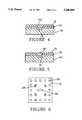
- FIG. 6is a top view of a typical device of the present invention. Shown is a device with layer 15 and contacts 16 on top of the device. Also shown is a device identification template 20 and alignment marks 19, Alignment marks are etched through layer 15, exposing the non-metallic passivation layer 12. In prior art devices, the alignment marks could not be etched in the passivation layer since metal circuitry under the passivation layer would be exposed.
Landscapes
- Engineering & Computer Science (AREA)
- Computer Hardware Design (AREA)
- Microelectronics & Electronic Packaging (AREA)
- Power Engineering (AREA)
- Physics & Mathematics (AREA)
- Condensed Matter Physics & Semiconductors (AREA)
- General Physics & Mathematics (AREA)
- Manufacturing & Machinery (AREA)
- Internal Circuitry In Semiconductor Integrated Circuit Devices (AREA)
- Wire Bonding (AREA)
Abstract
Description
This invention relates to semiconductor devices, and more particularly to the deposition of a non-corrosive metal barrier over semiconductor passivation to eliminate active metal circuit corrosion.
Present semiconductor technology includes depositing a nitride passivation coating over the surface of a semiconductor device. Bond pad metallization used with such passivation is typically aluminum which is susceptible to corrosion. Also pin holes in the nitride passivation allow corrosion products to contact underlying active metal of the semiconductor device.
Another process to prevent the corrosion products from affecting the semiconductor device uses a deposit of a noble metal in the form of a bump or cap on the bond pads in addition to the nitride passivation layer. However, pinholes in the nitride passivation coating still allow corrosion products to enter the pin holes and contact the underlying active metal on the semiconductor device.
The invention is a device and method for making the device which includes a deposited layer of a non-corrosive noble metal barrier over the semiconductor passivation to eliminate active metal circuit corrosion. This technique can be used in conjunction with the deposition of a multi metal layer "bump" or "cap" on the bond pads of the semiconductor device. Typical multi metal layers consist of deposition of a diffusion barrier metal such as Titanium-tungsten or chromium followed by deposition of a noble metal layer which may include, but is not limited to gold, palladium, platinum and ruthenium.
Several advantages result from the invention. An improved reliability due to protection of underlying active metal circuitry on the device surface from corrosion. Packaging material containing higher levels of ionic contaminants can be used, and such packaging materials are less expensive.
Another improvement results in enhanced electrical simultaneous switching performance due to the metal layer over the device surface serving as a noise filtering capacitor. The non-corrosive metal barrier provides an additional location upon which to place standardized bonding alignment targets which improve bonding process yields.
The invention reduces wafer fab manufacturing/waste treatment costs associated with the non-corrosive bond pad technique by leaving the barrier layer intact on the device. Previous processes etched away any barrier layer, except that on the bond pad, reexposing the existing device passivation.
The technical advance represented by the invention as well as the objects thereof will become apparent from the following description of a preferred embodiment of the invention when considered in conjunction with the accompanying drawings, and the novel features set forth in the appended claims.
FIG. 1 is a top view of a typical semiconductor chip with bond pads around the periphery;
FIG. 2 illustrates a cross-section view of asection 2--2 of FIG. 1, showing a prior art contact and passivation;
FIG. 3 illustrates a cross-sectional view ofsection 2--2 of FIG. 1, for hermetic bond pad technology;
FIG. 4 illustrates a cross-sectional view ofsection 2--2 of FIG. 1 for a non-corrosive barrier defined in the present invention;
FIG. 5 illustrates the non-corrosive layer and contact of the present invention; and
FIG. 6 is a top view of a device of the present invention illustrating alignment targets in the non-corrosive barrier layer.
FIG. 1 illustrates the top of asemiconductor chip 10 havingbond pads 11 around the periphery of the chip. Each bond pad is to a contact area on the semiconductor chip. The area around each bond pad is covered with a passivation non-conducting material to protect the top of the semiconductor chip and any circuitry on the chip surface.
FIG. 2 illustrates a prior art device.Semiconductor chip 10 has a non-metallic, non-conductive passivation coating 12 on the top of the chip. An opening is made in coating 12 to exposebond pad 13.Bond pad 13 is a conductive material, typically aluminum which is susceptible to corrosion.
FIG. 3 illustrates a prior art device in which anoble metal cap 14 is placed over thealuminum bond pad 13.Cap 14 covers and sealsaluminum bond pad 13, butpassivation 12, typically a nitride, can have pin holes through which corrosion material may contact the underlying surface of the semiconductor device.
FIG. 4 is a cross-sectional view of a device of the present invention, prior to its completion.Semiconductor device 10 hascontact pad 13 formed on the surface of the device. Apassivation layer 12 is placed over the surface ofdevice 10, and an opening 13a is made inlayer 12 to exposecontact pad 13. Alayer 15 of a non-corrosive metal material is formed overpassivation layer 12, filling opening 13a and contactingbond pad 13.
FIG. 5 is a cross-sectional view of the device of FIG. 4 afteretching layer 15 to provide a noncorrosive metal cap 16 onbond pad 13 and a covering non corrosive of metal on thepassivation layer 12.Layer 15 is etched around each bond pad to electrically isolate the bond pad from the remaining part oflayer 15. The remaining part oflayer 15 covers the entire surface ofdevice 10 not covered bybond pad cap 16.
FIG. 6 is a top view of a typical device of the present invention. Shown is a device withlayer 15 andcontacts 16 on top of the device. Also shown is adevice identification template 20 andalignment marks 19, Alignment marks are etched throughlayer 15, exposing thenon-metallic passivation layer 12. In prior art devices, the alignment marks could not be etched in the passivation layer since metal circuitry under the passivation layer would be exposed.
Claims (4)
1. A method for eliminating active metal circuit corrosion through the surface passivation layer and around contacts on a semiconductor device, comprising the steps of:
applying non-corrosive multi-layers of at least two different metals over the entire surface of the semiconductor device, including the passivation layer, and over the contacts on the semiconductor device;
etching the non-corrosive multi-layers to separate the non-corrosive multi-layers on the contacts from the non-corrosive multi-layers on the passivation layer to electrically isolate the contacts and the non-corrosive multi-layers thereon from the non-corrosive multi-layers on the passivation layer; and
leaving the non-corrosive multi-layers on the passivation layer on the completed semiconductor device.
2. The method according to claim 1, wherein said non-corrosive multi-layers have alignment marks formed therein.
3. The method according to claim 1, wherein said non-corrosive multi-layers include a device identification template.
4. A method for eliminating active metal circuit corrosion through the surface passivation layer, and around contacts on a semiconductor device, comprising the steps of:
applying non-corrosive multi-layers of metals over the entire surface of the semiconductor device, including the passivation layer, and over the contacts on the semiconductor device;
etching the non-corrosive multi-layers to separate the non-corrosive multi-layers on the contacts from the non-corrosive multi-layers on the passivation layer to electrically isolate the contacts and the non-corrosive multi-layers thereon from the non-corrosive multi-layers on the passivation layer;
leaving the non-corrosive multi-layers on the passivation layer on the completed semiconductor device.
Priority Applications (2)
| Application Number | Priority Date | Filing Date | Title |
|---|---|---|---|
| US07/914,832US5346858A (en) | 1992-07-16 | 1992-07-16 | Semiconductor non-corrosive metal overcoat |
| JP5175478AJPH06181233A (en) | 1992-07-16 | 1993-07-15 | Semiconductor device having eliminated corrosion of metal circuit and its method |
Applications Claiming Priority (1)
| Application Number | Priority Date | Filing Date | Title |
|---|---|---|---|
| US07/914,832US5346858A (en) | 1992-07-16 | 1992-07-16 | Semiconductor non-corrosive metal overcoat |
Publications (1)
| Publication Number | Publication Date |
|---|---|
| US5346858Atrue US5346858A (en) | 1994-09-13 |
Family
ID=25434830
Family Applications (1)
| Application Number | Title | Priority Date | Filing Date |
|---|---|---|---|
| US07/914,832Expired - LifetimeUS5346858A (en) | 1992-07-16 | 1992-07-16 | Semiconductor non-corrosive metal overcoat |
Country Status (2)
| Country | Link |
|---|---|
| US (1) | US5346858A (en) |
| JP (1) | JPH06181233A (en) |
Cited By (16)
| Publication number | Priority date | Publication date | Assignee | Title |
|---|---|---|---|---|
| EP0743676A3 (en)* | 1995-05-19 | 1998-01-07 | Matsushita Electric Industrial Co., Ltd. | Semiconductor device checking method |
| US5936311A (en)* | 1996-12-31 | 1999-08-10 | Intel Corporation | Integrated circuit alignment marks distributed throughout a surface metal line |
| US20020158334A1 (en)* | 2001-04-30 | 2002-10-31 | Intel Corporation | Microelectronic device having signal distribution functionality on an interfacial layer thereof |
| US20020173133A1 (en)* | 2001-05-21 | 2002-11-21 | Intel Corporation | Method for packaging a microelectronic device using on-die bond pad expansion |
| US6586276B2 (en)* | 2001-07-11 | 2003-07-01 | Intel Corporation | Method for fabricating a microelectronic device using wafer-level adhesion layer deposition |
| US20040183209A1 (en)* | 2003-03-17 | 2004-09-23 | Megic Corporation | High performance IC chip having discrete decoupling capacitors attached to its IC surface |
| US20040256704A1 (en)* | 2003-06-18 | 2004-12-23 | Intel Corporation | Apparatus and method extending flip-chip pad structures for wirebonding on low-k dielectric silicon |
| US20050090071A1 (en)* | 2003-10-28 | 2005-04-28 | Dower Joseph P. | Fabricating semiconductor chips |
| US6888240B2 (en) | 2001-04-30 | 2005-05-03 | Intel Corporation | High performance, low cost microelectronic circuit package with interposer |
| US20060208254A1 (en)* | 1997-08-08 | 2006-09-21 | California Institute Of Technology | Techniques and systems for analyte detection |
| US20060258143A1 (en)* | 2005-05-16 | 2006-11-16 | Taiwan Semiconductor Manufacturing Co., Ltd. | Method of reducing process steps in metal line protective structure formation |
| US7183658B2 (en) | 2001-09-05 | 2007-02-27 | Intel Corporation | Low cost microelectronic circuit package |
| US20070194460A1 (en)* | 2006-02-23 | 2007-08-23 | Chu-Chung Lee | Cap layer for an aluminum copper bond pad |
| US20070284751A1 (en)* | 1998-12-21 | 2007-12-13 | Mou-Shiung Lin | Top layers of metal for high performance IC's |
| US20080150623A1 (en)* | 2006-12-26 | 2008-06-26 | Megica Corporation | Voltage Regulator Integrated with Semiconductor Chip |
| US20100165585A1 (en)* | 2008-12-26 | 2010-07-01 | Megica Corporation | Chip packages with power management integrated circuits and related techniques |
Families Citing this family (2)
| Publication number | Priority date | Publication date | Assignee | Title |
|---|---|---|---|---|
| JP3962402B2 (en)* | 2003-11-10 | 2007-08-22 | 松下電器産業株式会社 | Semiconductor device |
| CN1617312A (en) | 2003-11-10 | 2005-05-18 | 松下电器产业株式会社 | Semiconductor device and manufacturing method thereof |
Citations (10)
| Publication number | Priority date | Publication date | Assignee | Title |
|---|---|---|---|---|
| US3997963A (en)* | 1973-06-29 | 1976-12-21 | Ibm Corporation | Novel beam-lead integrated circuit structure and method for making the same including automatic registration of beam-leads with corresponding dielectric substrate leads |
| US4742023A (en)* | 1986-08-28 | 1988-05-03 | Fujitsu Limited | Method for producing a semiconductor device |
| US4761386A (en)* | 1984-10-22 | 1988-08-02 | National Semiconductor Corporation | Method of fabricating conductive non-metallic self-passivating non-corrodable IC bonding pads |
| JPH02125447A (en)* | 1988-06-22 | 1990-05-14 | Hitachi Ltd | Semiconductor device and manufacture thereof |
| US4968637A (en)* | 1989-05-31 | 1990-11-06 | Raytheon Company | Method of manufacture TiW alignment mark and implant mask |
| US5026667A (en)* | 1987-12-29 | 1991-06-25 | Analog Devices, Incorporated | Producing integrated circuit chips with reduced stress effects |
| US5063655A (en)* | 1990-04-02 | 1991-11-12 | International Business Machines Corp. | Method to integrate drive/control devices and ink jet on demand devices in a single printhead chip |
| US5071518A (en)* | 1989-10-24 | 1991-12-10 | Microelectronics And Computer Technology Corporation | Method of making an electrical multilayer interconnect |
| US5078831A (en)* | 1990-03-30 | 1992-01-07 | Masafumi Miyazaki | Method of making multilayer printed wiring board |
| US5136364A (en)* | 1991-06-12 | 1992-08-04 | National Semiconductor Corporation | Semiconductor die sealing |
- 1992
- 1992-07-16USUS07/914,832patent/US5346858A/ennot_activeExpired - Lifetime
- 1993
- 1993-07-15JPJP5175478Apatent/JPH06181233A/enactivePending
Patent Citations (10)
| Publication number | Priority date | Publication date | Assignee | Title |
|---|---|---|---|---|
| US3997963A (en)* | 1973-06-29 | 1976-12-21 | Ibm Corporation | Novel beam-lead integrated circuit structure and method for making the same including automatic registration of beam-leads with corresponding dielectric substrate leads |
| US4761386A (en)* | 1984-10-22 | 1988-08-02 | National Semiconductor Corporation | Method of fabricating conductive non-metallic self-passivating non-corrodable IC bonding pads |
| US4742023A (en)* | 1986-08-28 | 1988-05-03 | Fujitsu Limited | Method for producing a semiconductor device |
| US5026667A (en)* | 1987-12-29 | 1991-06-25 | Analog Devices, Incorporated | Producing integrated circuit chips with reduced stress effects |
| JPH02125447A (en)* | 1988-06-22 | 1990-05-14 | Hitachi Ltd | Semiconductor device and manufacture thereof |
| US4968637A (en)* | 1989-05-31 | 1990-11-06 | Raytheon Company | Method of manufacture TiW alignment mark and implant mask |
| US5071518A (en)* | 1989-10-24 | 1991-12-10 | Microelectronics And Computer Technology Corporation | Method of making an electrical multilayer interconnect |
| US5078831A (en)* | 1990-03-30 | 1992-01-07 | Masafumi Miyazaki | Method of making multilayer printed wiring board |
| US5063655A (en)* | 1990-04-02 | 1991-11-12 | International Business Machines Corp. | Method to integrate drive/control devices and ink jet on demand devices in a single printhead chip |
| US5136364A (en)* | 1991-06-12 | 1992-08-04 | National Semiconductor Corporation | Semiconductor die sealing |
Cited By (39)
| Publication number | Priority date | Publication date | Assignee | Title |
|---|---|---|---|---|
| EP0743676A3 (en)* | 1995-05-19 | 1998-01-07 | Matsushita Electric Industrial Co., Ltd. | Semiconductor device checking method |
| US5936311A (en)* | 1996-12-31 | 1999-08-10 | Intel Corporation | Integrated circuit alignment marks distributed throughout a surface metal line |
| US5943588A (en)* | 1996-12-31 | 1999-08-24 | Intel Corporation | Method of manufacturing and using alignment marks |
| US20060208254A1 (en)* | 1997-08-08 | 2006-09-21 | California Institute Of Technology | Techniques and systems for analyte detection |
| US7550310B2 (en)* | 1997-08-08 | 2009-06-23 | California Institute Of Technology | Techniques and systems for analyte detection |
| US20090309614A1 (en)* | 1998-04-09 | 2009-12-17 | California Institute Of Technology | Techniques and systems for analyte detection |
| US20070284753A1 (en)* | 1998-12-21 | 2007-12-13 | Mou-Shiung Lin | Top layers of metal for high performance IC's |
| US20070284751A1 (en)* | 1998-12-21 | 2007-12-13 | Mou-Shiung Lin | Top layers of metal for high performance IC's |
| US7884479B2 (en) | 1998-12-21 | 2011-02-08 | Megica Corporation | Top layers of metal for high performance IC's |
| US7863654B2 (en) | 1998-12-21 | 2011-01-04 | Megica Corporation | Top layers of metal for high performance IC's |
| US8415800B2 (en) | 1998-12-21 | 2013-04-09 | Megica Corporation | Top layers of metal for high performance IC's |
| US7999384B2 (en) | 1998-12-21 | 2011-08-16 | Megica Corporation | Top layers of metal for high performance IC's |
| US8471384B2 (en) | 1998-12-21 | 2013-06-25 | Megica Corporation | Top layers of metal for high performance IC's |
| US8022545B2 (en) | 1998-12-21 | 2011-09-20 | Megica Corporation | Top layers of metal for high performance IC's |
| US8531038B2 (en) | 1998-12-21 | 2013-09-10 | Megica Corporation | Top layers of metal for high performance IC's |
| US20070284752A1 (en)* | 1998-12-21 | 2007-12-13 | Mou-Shiung Lin | Top layers of metal for high performance IC's |
| US6888240B2 (en) | 2001-04-30 | 2005-05-03 | Intel Corporation | High performance, low cost microelectronic circuit package with interposer |
| US6894399B2 (en) | 2001-04-30 | 2005-05-17 | Intel Corporation | Microelectronic device having signal distribution functionality on an interfacial layer thereof |
| US20020158334A1 (en)* | 2001-04-30 | 2002-10-31 | Intel Corporation | Microelectronic device having signal distribution functionality on an interfacial layer thereof |
| US20020173133A1 (en)* | 2001-05-21 | 2002-11-21 | Intel Corporation | Method for packaging a microelectronic device using on-die bond pad expansion |
| US7071024B2 (en)* | 2001-05-21 | 2006-07-04 | Intel Corporation | Method for packaging a microelectronic device using on-die bond pad expansion |
| US6586276B2 (en)* | 2001-07-11 | 2003-07-01 | Intel Corporation | Method for fabricating a microelectronic device using wafer-level adhesion layer deposition |
| US7183658B2 (en) | 2001-09-05 | 2007-02-27 | Intel Corporation | Low cost microelectronic circuit package |
| US20040183209A1 (en)* | 2003-03-17 | 2004-09-23 | Megic Corporation | High performance IC chip having discrete decoupling capacitors attached to its IC surface |
| US8368150B2 (en)* | 2003-03-17 | 2013-02-05 | Megica Corporation | High performance IC chip having discrete decoupling capacitors attached to its IC surface |
| US7262513B2 (en) | 2003-06-18 | 2007-08-28 | Intel Corporation | Apparatus and method extending flip-chip pad structures for wirebonding on low-k dielectric silicon |
| US20040256704A1 (en)* | 2003-06-18 | 2004-12-23 | Intel Corporation | Apparatus and method extending flip-chip pad structures for wirebonding on low-k dielectric silicon |
| US20050258549A1 (en)* | 2003-06-18 | 2005-11-24 | Intel Corporation | Apparatus and method extending flip-chip pad structures for wirebonding on low-k dielectric silicon |
| US6927156B2 (en)* | 2003-06-18 | 2005-08-09 | Intel Corporation | Apparatus and method extending flip-chip pad structures for wirebonding on low-k dielectric silicon |
| US6975040B2 (en)* | 2003-10-28 | 2005-12-13 | Agere Systems Inc | Fabricating semiconductor chips |
| US20050090071A1 (en)* | 2003-10-28 | 2005-04-28 | Dower Joseph P. | Fabricating semiconductor chips |
| US20060258143A1 (en)* | 2005-05-16 | 2006-11-16 | Taiwan Semiconductor Manufacturing Co., Ltd. | Method of reducing process steps in metal line protective structure formation |
| US7495335B2 (en)* | 2005-05-16 | 2009-02-24 | Taiwan Semiconductor Manufacturing Co., Ltd. | Method of reducing process steps in metal line protective structure formation |
| US20070194460A1 (en)* | 2006-02-23 | 2007-08-23 | Chu-Chung Lee | Cap layer for an aluminum copper bond pad |
| US7656045B2 (en) | 2006-02-23 | 2010-02-02 | Freescale Semiconductor, Inc. | Cap layer for an aluminum copper bond pad |
| US20080150623A1 (en)* | 2006-12-26 | 2008-06-26 | Megica Corporation | Voltage Regulator Integrated with Semiconductor Chip |
| US8749021B2 (en) | 2006-12-26 | 2014-06-10 | Megit Acquisition Corp. | Voltage regulator integrated with semiconductor chip |
| US20100165585A1 (en)* | 2008-12-26 | 2010-07-01 | Megica Corporation | Chip packages with power management integrated circuits and related techniques |
| US8809951B2 (en) | 2008-12-26 | 2014-08-19 | Megit Acquisition Corp. | Chip packages having dual DMOS devices with power management integrated circuits |
Also Published As
| Publication number | Publication date |
|---|---|
| JPH06181233A (en) | 1994-06-28 |
Similar Documents
| Publication | Publication Date | Title |
|---|---|---|
| US5346858A (en) | Semiconductor non-corrosive metal overcoat | |
| US6451681B1 (en) | Method of forming copper interconnection utilizing aluminum capping film | |
| US6187680B1 (en) | Method/structure for creating aluminum wirebound pad on copper BEOL | |
| US6630736B1 (en) | Light barrier for light sensitive semiconductor devices | |
| US5707894A (en) | Bonding pad structure and method thereof | |
| EP0076856A1 (en) | Method of making a semiconductor device having a projecting, plated electrode | |
| US5059553A (en) | Metal bump for a thermal compression bond and method for making same | |
| US6144100A (en) | Integrated circuit with bonding layer over active circuitry | |
| US7880300B2 (en) | Semiconductor chip comprising a metal coating structure and associated production method | |
| HK1049913A1 (en) | Metal redistribution layer having solderable pads and wire bondable pads | |
| US9852940B2 (en) | Method for forming a reliable solderable contact | |
| KR100365166B1 (en) | Method and apparatus for capping metallization layer | |
| US5776801A (en) | Leadframe having contact pads defined by a polymer insulating film | |
| US5436198A (en) | Method of manufacturing semiconductor device having straight wall bump | |
| KR20090009890A (en) | Contacts and Methods Surrounded by Passivation and Polyimide | |
| US4622576A (en) | Conductive non-metallic self-passivating non-corrodable IC bonding pads | |
| US4394678A (en) | Elevated edge-protected bonding pedestals for semiconductor devices | |
| US6327158B1 (en) | Metal pads for electrical probe testing on wafer with bump interconnects | |
| US4680610A (en) | Semiconductor component comprising bump-like, metallic lead contacts and multilayer wiring | |
| US6972496B2 (en) | Chip-scaled package having a sealed connection wire | |
| CA2075462C (en) | Bump structure and method for bonding to a semi-conductor device | |
| US5053851A (en) | Metal bump for a thermal compression bond and method for making same | |
| US7327030B2 (en) | Apparatus and method incorporating discrete passive components in an electronic package | |
| JP2674567B2 (en) | Semiconductor device | |
| US20050186772A1 (en) | Process for producing metallic interconnects and contact surfaces on electronic components |
Legal Events
| Date | Code | Title | Description |
|---|---|---|---|
| AS | Assignment | Owner name:TEXAS INSTRUMENTS INCORPORATED, TEXAS Free format text:ASSIGNMENT OF ASSIGNORS INTEREST.;ASSIGNORS:THOMAS, JAMES R.;NYE, LARRY W.;BROOK, RICHARD M.;REEL/FRAME:006207/0826;SIGNING DATES FROM 19920515 TO 19920714 | |
| STCF | Information on status: patent grant | Free format text:PATENTED CASE | |
| FEPP | Fee payment procedure | Free format text:PAYOR NUMBER ASSIGNED (ORIGINAL EVENT CODE: ASPN); ENTITY STATUS OF PATENT OWNER: LARGE ENTITY | |
| FPAY | Fee payment | Year of fee payment:4 | |
| FPAY | Fee payment | Year of fee payment:8 | |
| FPAY | Fee payment | Year of fee payment:12 |