US5345564A - Serial communication peripheral integrated electronic circuit that recognizes its unique address before the entire circuit is enabled - Google Patents
Serial communication peripheral integrated electronic circuit that recognizes its unique address before the entire circuit is enabledDownload PDFInfo
- Publication number
- US5345564A US5345564AUS07/861,298US86129892AUS5345564AUS 5345564 AUS5345564 AUS 5345564AUS 86129892 AUS86129892 AUS 86129892AUS 5345564 AUS5345564 AUS 5345564A
- Authority
- US
- United States
- Prior art keywords
- peripheral
- cpu
- data
- identification code
- circuit
- Prior art date
- Legal status (The legal status is an assumption and is not a legal conclusion. Google has not performed a legal analysis and makes no representation as to the accuracy of the status listed.)
- Expired - Lifetime
Links
Images

Classifications
- G—PHYSICS
- G06—COMPUTING OR CALCULATING; COUNTING
- G06F—ELECTRIC DIGITAL DATA PROCESSING
- G06F1/00—Details not covered by groups G06F3/00 - G06F13/00 and G06F21/00
- G06F1/26—Power supply means, e.g. regulation thereof
- G06F1/32—Means for saving power
- G06F1/3203—Power management, i.e. event-based initiation of a power-saving mode
- G06F1/3234—Power saving characterised by the action undertaken
- G06F1/3237—Power saving characterised by the action undertaken by disabling clock generation or distribution
- G—PHYSICS
- G06—COMPUTING OR CALCULATING; COUNTING
- G06F—ELECTRIC DIGITAL DATA PROCESSING
- G06F1/00—Details not covered by groups G06F3/00 - G06F13/00 and G06F21/00
- G06F1/26—Power supply means, e.g. regulation thereof
- G06F1/32—Means for saving power
- G06F1/3203—Power management, i.e. event-based initiation of a power-saving mode
- G06F1/3234—Power saving characterised by the action undertaken
- G06F1/325—Power saving in peripheral device
- G—PHYSICS
- G06—COMPUTING OR CALCULATING; COUNTING
- G06F—ELECTRIC DIGITAL DATA PROCESSING
- G06F13/00—Interconnection of, or transfer of information or other signals between, memories, input/output devices or central processing units
- G06F13/38—Information transfer, e.g. on bus
- G06F13/42—Bus transfer protocol, e.g. handshake; Synchronisation
- G06F13/4204—Bus transfer protocol, e.g. handshake; Synchronisation on a parallel bus
- G06F13/4221—Bus transfer protocol, e.g. handshake; Synchronisation on a parallel bus being an input/output bus, e.g. ISA bus, EISA bus, PCI bus, SCSI bus
- G06F13/423—Bus transfer protocol, e.g. handshake; Synchronisation on a parallel bus being an input/output bus, e.g. ISA bus, EISA bus, PCI bus, SCSI bus with synchronous protocol
- Y—GENERAL TAGGING OF NEW TECHNOLOGICAL DEVELOPMENTS; GENERAL TAGGING OF CROSS-SECTIONAL TECHNOLOGIES SPANNING OVER SEVERAL SECTIONS OF THE IPC; TECHNICAL SUBJECTS COVERED BY FORMER USPC CROSS-REFERENCE ART COLLECTIONS [XRACs] AND DIGESTS
- Y02—TECHNOLOGIES OR APPLICATIONS FOR MITIGATION OR ADAPTATION AGAINST CLIMATE CHANGE
- Y02D—CLIMATE CHANGE MITIGATION TECHNOLOGIES IN INFORMATION AND COMMUNICATION TECHNOLOGIES [ICT], I.E. INFORMATION AND COMMUNICATION TECHNOLOGIES AIMING AT THE REDUCTION OF THEIR OWN ENERGY USE
- Y02D10/00—Energy efficient computing, e.g. low power processors, power management or thermal management
Definitions
- This inventionis related generally to computer system peripheral integrated circuits and their use, and, more specifically, to a technique and circuit for enabling a master processing unit to select one of several peripheral circuits having slave processing units for data communication with the master.
- a commonly used technique for transferring data between a central processing unit (“CPU”) and a selected one of several peripheral circuitsis by serial communication.
- a known serial peripheral interface (“SPI")utilizes four lines for full duplex communication, one line for digital data being received by the peripheral, another for digital data being sent by the peripheral, another for a clock signal and another for a select line.
- Half duplex communicationrequires only three lines, the line to send data from the peripheral not being utilized. All of these lines are connected between the CPU, acting as a master device, and each of the peripheral circuits, acting as slaves.
- a single lineis utilized with a first data word transmitted by the CPU to each of the peripherals containing an identification of the one peripheral with which the CPU is to establish data communication.
- the unique identification code within each of the peripheralsis then compared with that first data word, and the peripheral that detects a positive comparison enables itself for the communication while the other peripherals remain in a passive state.
- This identification code comparisonis usually accomplished by a slave processor that exists as part of each of the peripheral circuits executing a software routine. It is a primary object of the present invention to improve this peripheral identification technique.
- a small hardwired circuitis provided at each interface of the slave peripheral with the master CPU that compares the first data word received from the CPU with an internally programmed unique identification code.
- the remainder of the peripheralincluding its processor and other active circuitry, is enabled only after a positive comparison is made. Only the small amount of comparator circuitry of each peripheral is awakened by the CPU when a communication link is to be established.
- the active portion of each of the peripherals in the systemremains asleep except for that of the one peripheral having an internally stored identification code that matches the peripheral selecting data word sent by the CPU.
- a primary advantage of this techniqueis a reduction in the amount of power consumed by the peripheral circuits, and thus a reduction in the power that must be supplied to a computer system that includes two or more such peripherals.
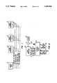
- FIG. 1schematically illustrates a computing system utilizing a plurality of peripheral circuits that incorporates the improvement of the present invention
- FIG. 2is a block diagram of each of the peripherals (slaves) shown in the block diagram of FIG. 1;
- FIG. 3illustrates one implementation of the interface circuits of FIG. 2.
- FIGS. 4(A)-4(E)provide a timing diagram illustrating an operation of the system of FIG. 1 with peripherals of the type illustrated in FIGS. 2 and 3.
- a digital systemincludes a master unit 11 and a plurality of slave units 13, 15 . . . 17.
- An example of such a systemis a special purpose computer system wherein the master unit 11 is a system CPU and each of the slave units 13, 15 . . . 17 is a peripheral circuit that interfaces with various elements and systems outside of the computer system shown in FIG. 1.
- the peripheral circuits 13, 15 . . . 17are connected in parallel with each other and the CPU 11 through four circuits to establish full duplex communication between the CPU and the various peripherals as selected.
- These circuitsusually a single conductor, include a line 19 transmitting data from the CPU to the peripherals, a line 21 for transmitting data from the peripherals to the CPU 11, a line 23 for the CPU to supply an operating clock signal to the peripherals, and a line 25 providing a control signal that designates when transfer of data is occurring between the CPU 11 and one or more peripherals 13, 15 . . . 17.
- This "slave select" signal in line 25is shown in FIG. 4(A) in a system timing diagram example.
- the clock signal on line 23is shown in FIG. 4(B) and the timing of a data transfer in either of the lines 19 or 21 shown in FIG. 4(C).
- the technique of the present inventionapplies to a system with two or more peripherals, "n" peripherals being shown in the system of FIG. 1.
- FIG. 2a block diagram showing the overall construction of each of the peripheral circuits 13, 15 . . . 17 of FIG. 1 is shown.
- Each of the four lines 19, 21, 23 and 25connects with an interface circuit 27, which itself is shown in more detail in FIG. 3.
- the processor 29is connected with the interface circuit 27 through a read/write line 31, internal data and address busses 33 and 35, and a line 37 that provides a signal when a character byte has been received by the interface circuit 27.
- An example of this signalis provided as part of the timing diagram in FIG. 4(D).
- the slave processor 29is driven by a separate clock source 39 through a switching element 41 that is controlled by a signal and a control line 43.
- the line 43becomes active in a pulse that indicates the interface circuit 27 has determined that this peripheral is being accessed by the system CPU 11.
- the switch 41connects the clock 39 to drive the slave processor 29.
- the slave processor 29has no clock signal connected to it and, particularly if implemented in complimentary metal-oxide-silicon ("CMOS"), results in the slave processor 29 consuming substantially no power during those periods when the peripheral is not being accessed.
- CMOScomplimentary metal-oxide-silicon
- the interface circuits 27 of each of the peripherals 13, 15 . . . 17are thus enabled when the clock signal in the common line 23 is turned on, these circuits are a small part of each peripheral and thus those in the peripheral not being accessed at the moment consume very little power.
- FIG. 3shows such in interface circuit 27.
- a control register 45is provided for storing a unique identification (address) code of the peripheral, usually in a byte of binary data. This code is loaded into the register 45 in a normal manner, such as during an initialization routine controlled by the system CPU 11 when power is first turned onto the system after a period of no operation.
- a companion receive register 47serially receives data on the line 19 from the system CPU 11 and issues the signal in line 37 (FIG. 4(D)) in the line 37 when a predetermined number of data bits have been received, conveniently eight bits to form one byte. Data is then communicated internally of the interface circuit 27 and with the peripheral slave processor 29 in parallel.
- FIGS. 4(A)-4(E)This comparison in data transmission operation is best illustrated in the timing diagram of FIGS. 4(A)-4(E).
- the slave select line 25(FIG. 4(A)) goes active, the first data word is clocked into the receive register 47 of each of the peripherals 13, 15 . . . 17 over the line 19.
- this first byte of datahas been received, as indicated by FIG. 4(C), and, if a positive comparison of that byte with the identification code of the peripheral is made, the awakening signal in line 43 goes active at that same time, as shown by a negative going pulse in FIG. 4(E).
- the desired datais then transferred between the selected peripheral and the master CPU, as shown by FIG. 4(C).
- the received character signal in line 37goes active (FIG. 4(D).
- each of the registers 45 and 47in operation of the comparative circuit 49, is controlled from a control logic circuit 59 through various control lines extending therefrom.
- An additional register 61serves to receive a byte of data in parallel from the slave processor 29 over the internal data bus 33, and then serially to the system CPU 11 over the line 21.
- this latter register 61is not involved in the peripheral selection or a power control function described previously. Even so, it can been seen from FIG. 3 the small number of elements that are powered up and rendered operational when the system CPU 11 starts the SPI clock signal in line 23. Little power is consumed in this circuit until, and unless, the peripheral incorporating it is chosen to become operational.
Landscapes
- Engineering & Computer Science (AREA)
- Theoretical Computer Science (AREA)
- Physics & Mathematics (AREA)
- General Engineering & Computer Science (AREA)
- General Physics & Mathematics (AREA)
- Information Transfer Systems (AREA)
Abstract
Description
Claims (3)
Priority Applications (1)
| Application Number | Priority Date | Filing Date | Title |
|---|---|---|---|
| US07/861,298US5345564A (en) | 1992-03-31 | 1992-03-31 | Serial communication peripheral integrated electronic circuit that recognizes its unique address before the entire circuit is enabled |
Applications Claiming Priority (1)
| Application Number | Priority Date | Filing Date | Title |
|---|---|---|---|
| US07/861,298US5345564A (en) | 1992-03-31 | 1992-03-31 | Serial communication peripheral integrated electronic circuit that recognizes its unique address before the entire circuit is enabled |
Publications (1)
| Publication Number | Publication Date |
|---|---|
| US5345564Atrue US5345564A (en) | 1994-09-06 |
Family
ID=25335428
Family Applications (1)
| Application Number | Title | Priority Date | Filing Date |
|---|---|---|---|
| US07/861,298Expired - LifetimeUS5345564A (en) | 1992-03-31 | 1992-03-31 | Serial communication peripheral integrated electronic circuit that recognizes its unique address before the entire circuit is enabled |
Country Status (1)
| Country | Link |
|---|---|
| US (1) | US5345564A (en) |
Cited By (22)
| Publication number | Priority date | Publication date | Assignee | Title |
|---|---|---|---|---|
| US5572685A (en)* | 1994-03-23 | 1996-11-05 | International Computers Limited | Computer system |
| US5594879A (en)* | 1993-10-29 | 1997-01-14 | Compaq Computer Corporation | Method of and apparatus for arbitrarily disabling under processor control individual slots on a computer bus |
| US5617572A (en)* | 1995-01-31 | 1997-04-01 | Dell Usa, L.P. | System for reducing power consumption in computers |
| US5630152A (en)* | 1992-05-18 | 1997-05-13 | Motorola, Inc. | Communication protocol between master and slave device with register information sharing |
| GB2308469A (en)* | 1995-12-22 | 1997-06-25 | Motorola Inc | Power conserving clocking system |
| US5666538A (en)* | 1995-06-07 | 1997-09-09 | Ast Research, Inc. | Disk power manager for network servers |
| US5682548A (en)* | 1993-08-12 | 1997-10-28 | Databook, Incorporated | Interface component for coupling main bus of computer system to peripheral ports having windows each includes bit specifying whether operations are quiet or not quiet |
| EP0814412A1 (en)* | 1996-06-19 | 1997-12-29 | Motorola, Inc. | A digital signal processor and a method for interfacing a digital signal processor |
| US5797038A (en)* | 1996-09-09 | 1998-08-18 | Ford Motor Company | Method and system for serially based host/peripheral communication |
| US5832286A (en)* | 1991-12-04 | 1998-11-03 | Sharp Kabushiki Kaisha | Power control apparatus for digital electronic device |
| US6032254A (en)* | 1996-04-26 | 2000-02-29 | Oki Electric Industry Co., Ltd. | Method of identifying peripheral device employed in a semiconductor device |
| US6078852A (en)* | 1996-12-18 | 2000-06-20 | Robert Bosch Gmbh | Method and device for administering wake times |
| WO2001009705A3 (en)* | 1999-08-03 | 2001-11-15 | Btech Inc | Serial bus communications system |
| WO2002041124A3 (en)* | 2000-11-15 | 2003-03-13 | Koninkl Philips Electronics Nv | Power management method and arrangement for bus-coupled circuit blocks |
| US20050198418A1 (en)* | 2004-03-02 | 2005-09-08 | Nec Electronics Corporation | Multilayer system and clock control method |
| US20060129722A1 (en)* | 2004-12-14 | 2006-06-15 | Rockwell Automation Technologies, Inc. | Low protocol, high speed serial transfer for intra-board or inter-board data communication |
| EP1008030B1 (en)* | 1996-12-16 | 2007-04-25 | Intel Corporation | Method and apparatus for supporting power conservation operation modes |
| CN1320471C (en)* | 2004-11-30 | 2007-06-06 | 北京中星微电子有限公司 | Half duplex series communication bus external device interface |
| GB2447794A (en)* | 2007-03-23 | 2008-09-24 | Intel Corp | Downstream cycle-aware dynamic interconnect isolation |
| US20090265494A1 (en)* | 2008-04-22 | 2009-10-22 | Seiko Epson Corporation | Data transmission and reception system, master device, and slave device |
| US20150109026A1 (en)* | 2013-10-22 | 2015-04-23 | Hon Hai Precision Industry Co., Ltd. | Electronic device assembly |
| US10313859B2 (en)* | 2015-01-21 | 2019-06-04 | Zhenhua Li | Personal working system capable of being dynamically combined and adjusted |
Citations (3)
| Publication number | Priority date | Publication date | Assignee | Title |
|---|---|---|---|---|
| US4615005A (en)* | 1980-10-27 | 1986-09-30 | Hitachi, Ltd. | Data processing apparatus with clock signal control by microinstruction for reduced power consumption and method therefor |
| US4841440A (en)* | 1983-04-26 | 1989-06-20 | Nec Corporation | Control processor for controlling a peripheral unit |
| US5111423A (en)* | 1988-07-21 | 1992-05-05 | Altera Corporation | Programmable interface for computer system peripheral circuit card |
- 1992
- 1992-03-31USUS07/861,298patent/US5345564A/ennot_activeExpired - Lifetime
Patent Citations (3)
| Publication number | Priority date | Publication date | Assignee | Title |
|---|---|---|---|---|
| US4615005A (en)* | 1980-10-27 | 1986-09-30 | Hitachi, Ltd. | Data processing apparatus with clock signal control by microinstruction for reduced power consumption and method therefor |
| US4841440A (en)* | 1983-04-26 | 1989-06-20 | Nec Corporation | Control processor for controlling a peripheral unit |
| US5111423A (en)* | 1988-07-21 | 1992-05-05 | Altera Corporation | Programmable interface for computer system peripheral circuit card |
Cited By (35)
| Publication number | Priority date | Publication date | Assignee | Title |
|---|---|---|---|---|
| US5832286A (en)* | 1991-12-04 | 1998-11-03 | Sharp Kabushiki Kaisha | Power control apparatus for digital electronic device |
| US5630152A (en)* | 1992-05-18 | 1997-05-13 | Motorola, Inc. | Communication protocol between master and slave device with register information sharing |
| US5682548A (en)* | 1993-08-12 | 1997-10-28 | Databook, Incorporated | Interface component for coupling main bus of computer system to peripheral ports having windows each includes bit specifying whether operations are quiet or not quiet |
| US5594879A (en)* | 1993-10-29 | 1997-01-14 | Compaq Computer Corporation | Method of and apparatus for arbitrarily disabling under processor control individual slots on a computer bus |
| US5572685A (en)* | 1994-03-23 | 1996-11-05 | International Computers Limited | Computer system |
| US5617572A (en)* | 1995-01-31 | 1997-04-01 | Dell Usa, L.P. | System for reducing power consumption in computers |
| US5666538A (en)* | 1995-06-07 | 1997-09-09 | Ast Research, Inc. | Disk power manager for network servers |
| US5961613A (en)* | 1995-06-07 | 1999-10-05 | Ast Research, Inc. | Disk power manager for network servers |
| EP0783148A3 (en)* | 1995-12-22 | 1999-08-25 | Motorola, Inc. | Power conserving clocking system |
| GB2308469A (en)* | 1995-12-22 | 1997-06-25 | Motorola Inc | Power conserving clocking system |
| US6032254A (en)* | 1996-04-26 | 2000-02-29 | Oki Electric Industry Co., Ltd. | Method of identifying peripheral device employed in a semiconductor device |
| SG88761A1 (en)* | 1996-04-26 | 2002-05-21 | Oki Electric Ind Co Ltd | Method of identifying peripheral device employed in a semiconductor device |
| EP0814412A1 (en)* | 1996-06-19 | 1997-12-29 | Motorola, Inc. | A digital signal processor and a method for interfacing a digital signal processor |
| US5797038A (en)* | 1996-09-09 | 1998-08-18 | Ford Motor Company | Method and system for serially based host/peripheral communication |
| EP1008030B1 (en)* | 1996-12-16 | 2007-04-25 | Intel Corporation | Method and apparatus for supporting power conservation operation modes |
| US6078852A (en)* | 1996-12-18 | 2000-06-20 | Robert Bosch Gmbh | Method and device for administering wake times |
| US6463543B1 (en) | 1999-08-03 | 2002-10-08 | Btech, Inc. | Serial bus communications system |
| WO2001009705A3 (en)* | 1999-08-03 | 2001-11-15 | Btech Inc | Serial bus communications system |
| KR100895543B1 (en) | 2000-11-15 | 2009-04-29 | 엔엑스피 비 브이 | Power Management System and Power Management Methods |
| US6694441B1 (en) | 2000-11-15 | 2004-02-17 | Koninklijke Philips Electronics N.V. | Power management method and arrangement for bus-coupled circuit blocks |
| WO2002041124A3 (en)* | 2000-11-15 | 2003-03-13 | Koninkl Philips Electronics Nv | Power management method and arrangement for bus-coupled circuit blocks |
| US20050198418A1 (en)* | 2004-03-02 | 2005-09-08 | Nec Electronics Corporation | Multilayer system and clock control method |
| US7277976B2 (en)* | 2004-03-02 | 2007-10-02 | Nec Electronics Corporation | Multilayer system and clock control method |
| CN1320471C (en)* | 2004-11-30 | 2007-06-06 | 北京中星微电子有限公司 | Half duplex series communication bus external device interface |
| US20060129722A1 (en)* | 2004-12-14 | 2006-06-15 | Rockwell Automation Technologies, Inc. | Low protocol, high speed serial transfer for intra-board or inter-board data communication |
| US7243173B2 (en)* | 2004-12-14 | 2007-07-10 | Rockwell Automation Technologies, Inc. | Low protocol, high speed serial transfer for intra-board or inter-board data communication |
| GB2447794A (en)* | 2007-03-23 | 2008-09-24 | Intel Corp | Downstream cycle-aware dynamic interconnect isolation |
| US20080235422A1 (en)* | 2007-03-23 | 2008-09-25 | Dhinesh Sasidaran | Downstream cycle-aware dynamic interconnect isolation |
| US20090265494A1 (en)* | 2008-04-22 | 2009-10-22 | Seiko Epson Corporation | Data transmission and reception system, master device, and slave device |
| US8082377B2 (en)* | 2008-04-22 | 2011-12-20 | Seiko Epson Corporation | Data transmission and reception system, master device, and slave device |
| US20150109026A1 (en)* | 2013-10-22 | 2015-04-23 | Hon Hai Precision Industry Co., Ltd. | Electronic device assembly |
| US9667254B2 (en)* | 2013-10-22 | 2017-05-30 | Hon Hai Precision Industry Co., Ltd. | Electronic device assembly |
| US10313859B2 (en)* | 2015-01-21 | 2019-06-04 | Zhenhua Li | Personal working system capable of being dynamically combined and adjusted |
| US10531260B2 (en) | 2015-01-21 | 2020-01-07 | Zhenhua Li | Personal working system capable of being dynamically combined and adjusted |
| CN111814126A (en)* | 2015-01-21 | 2020-10-23 | 李振华 | A personal work system that can be dynamically combined and adjusted |
Similar Documents
| Publication | Publication Date | Title |
|---|---|---|
| US5345564A (en) | Serial communication peripheral integrated electronic circuit that recognizes its unique address before the entire circuit is enabled | |
| US5021950A (en) | Multiprocessor system with standby function | |
| US4841440A (en) | Control processor for controlling a peripheral unit | |
| US7529862B2 (en) | System for providing access of multiple data buffers to a data retaining and processing device | |
| CA1335843C (en) | Programmable option select | |
| US5802269A (en) | Method and apparatus for power management of distributed direct memory access (DDMA) devices | |
| EP0458304B1 (en) | Direct memory access transfer controller and use | |
| US4984190A (en) | Serial data transfer system | |
| US5778195A (en) | PC card | |
| JPH0677249B2 (en) | Microcomputer | |
| US7822076B2 (en) | Apparatus for multiplexing signals through I/O pins | |
| US4622630A (en) | Data processing system having unique bus control protocol | |
| US5954813A (en) | Data processor with transparent operation during a background mode and method therefor | |
| EP0996068A2 (en) | Deterministic arbitration of a serial bus using arbitration addresses | |
| EP0478149A2 (en) | Workstation and method of configuring same | |
| US5019962A (en) | Direct memory access controller for a multi-microcomputer system | |
| US20040015615A1 (en) | Method for performing data transfer of KVM switch | |
| US6751689B2 (en) | Interface circuit and method for transmitting data between a serial interface and a processor | |
| US5371863A (en) | High speed processor bus extension | |
| US8060676B2 (en) | Method of hot switching data transfer rate on bus | |
| US20030200401A1 (en) | Microcomputer system automatically backing-up data written in storage medium in transceiver, and transceiver connected thereto | |
| EP0783148A2 (en) | Power conserving clocking system | |
| US5222227A (en) | Direct memory access controller for a multi-microcomputer system | |
| EP0473278B1 (en) | Logic apparatus for use with a computing device | |
| US6018781A (en) | Work station having simultaneous access to registers contained in two different interfaces |
Legal Events
| Date | Code | Title | Description |
|---|---|---|---|
| AS | Assignment | Owner name:ZILOG, INC., CALIFORNIA Free format text:ASSIGNMENT OF ASSIGNORS INTEREST.;ASSIGNORS:JENSEN, BRADLEY D.;MORSON, ED;REEL/FRAME:006199/0479;SIGNING DATES FROM 19920528 TO 19920611 | |
| STCF | Information on status: patent grant | Free format text:PATENTED CASE | |
| FEPP | Fee payment procedure | Free format text:PAYOR NUMBER ASSIGNED (ORIGINAL EVENT CODE: ASPN); ENTITY STATUS OF PATENT OWNER: LARGE ENTITY | |
| FPAY | Fee payment | Year of fee payment:4 | |
| AS | Assignment | Owner name:STATE STREET BANK AND TRUST COMPANY, CONNECTICUT Free format text:SECURITY INTEREST;ASSIGNOR:ZILOG, INC.;REEL/FRAME:009089/0001 Effective date:19980227 | |
| FPAY | Fee payment | Year of fee payment:8 | |
| FPAY | Fee payment | Year of fee payment:12 | |
| AS | Assignment | Owner name:ZILOG, INC., CALIFORNIA Free format text:U.S. BANKRUPTCY COURT FOR NORTHERN DISTRICT OF CALIFORNIA ORDER RELEASING ALL LIENS;ASSIGNOR:STATE STREET BANK AND TRUST COMPANY;REEL/FRAME:022868/0934 Effective date:20020430 | |
| AS | Assignment | Owner name:IXYS CH GMBH, SWITZERLAND Free format text:ASSIGNMENT OF ASSIGNORS INTEREST;ASSIGNOR:ZILOG, INC.;REEL/FRAME:024964/0132 Effective date:20100217 | |
| AS | Assignment | Owner name:IXYS INTL LIMITED, CAYMAN ISLANDS Free format text:ASSIGNMENT OF ASSIGNORS INTEREST;ASSIGNOR:IXYS CH GMBH;REEL/FRAME:035663/0618 Effective date:20150515 |