US5345256A - High density interconnect apparatus for an ink jet printhead - Google Patents
High density interconnect apparatus for an ink jet printheadDownload PDFInfo
- Publication number
- US5345256A US5345256AUS08/020,050US2005093AUS5345256AUS 5345256 AUS5345256 AUS 5345256AUS 2005093 AUS2005093 AUS 2005093AUS 5345256 AUS5345256 AUS 5345256A
- Authority
- US
- United States
- Prior art keywords
- electrically conductive
- array
- printhead
- top side
- mounting plate
- Prior art date
- Legal status (The legal status is an assumption and is not a legal conclusion. Google has not performed a legal analysis and makes no representation as to the accuracy of the status listed.)
- Expired - Lifetime
Links
Images
Classifications
- B—PERFORMING OPERATIONS; TRANSPORTING
- B41—PRINTING; LINING MACHINES; TYPEWRITERS; STAMPS
- B41J—TYPEWRITERS; SELECTIVE PRINTING MECHANISMS, i.e. MECHANISMS PRINTING OTHERWISE THAN FROM A FORME; CORRECTION OF TYPOGRAPHICAL ERRORS
- B41J2/00—Typewriters or selective printing mechanisms characterised by the printing or marking process for which they are designed
- B41J2/005—Typewriters or selective printing mechanisms characterised by the printing or marking process for which they are designed characterised by bringing liquid or particles selectively into contact with a printing material
- B41J2/01—Ink jet
- B41J2/135—Nozzles
- B41J2/14—Structure thereof only for on-demand ink jet heads
- B41J2/14201—Structure of print heads with piezoelectric elements
- B41J2/14209—Structure of print heads with piezoelectric elements of finger type, chamber walls consisting integrally of piezoelectric material
- B—PERFORMING OPERATIONS; TRANSPORTING
- B41—PRINTING; LINING MACHINES; TYPEWRITERS; STAMPS
- B41J—TYPEWRITERS; SELECTIVE PRINTING MECHANISMS, i.e. MECHANISMS PRINTING OTHERWISE THAN FROM A FORME; CORRECTION OF TYPOGRAPHICAL ERRORS
- B41J2/00—Typewriters or selective printing mechanisms characterised by the printing or marking process for which they are designed
- B41J2/005—Typewriters or selective printing mechanisms characterised by the printing or marking process for which they are designed characterised by bringing liquid or particles selectively into contact with a printing material
- B41J2/01—Ink jet
- B41J2/135—Nozzles
- B41J2/14—Structure thereof only for on-demand ink jet heads
- B41J2002/14379—Edge shooter
Definitions
- the present inventiongenerally relates to ink jet printhead apparatus and more particularly relates to apparatus for operatively interconnecting an ink jet printhead to an electrical power supply source used to control and piezoelectrically drive the printhead.
- a piezoelectrically actuated in jet printheadis a relatively small device used to selectively eject tiny ink droplets onto a paper sheet operatively fed through a printer, in which the printhead is incorporated, to thereby form from the ejected ink droplets selected text and/or graphics on the sheet.
- an ink jet printheadhas a horizontally spaced parallel array of internal ink-receiving channels. These internal channels are covered at their front ends by a plate member through which a spaced series of small ink discharge orifices are formed. Each channel opens outwardly through a different one of the spaced orifices.
- a spaced series of internal piezoelectric wall portions of the printhead bodyseparate and laterally bound the channels along their lengths.
- the two printhead sidewall portions that laterally bound the channel associated with the selected orificeare piezoelectrically deflected into the channel and then returned to their normal undeflected positions.
- the driven inward deflection of the opposite channel wall portionsincreases the pressure of the ink within the channel sufficiently to force a small quantity of ink, in droplet form, outwardly through the discharge orifice.
- the electrical signals required to create and control the requisite printhead channel side wall deflectionsare typically generated by a suitable electronic driver. Due to the large number of very closely spaced ink channels present in even a small ink jet printhead structure, the resulting number of these electrical signals is quite high, while the physical area available at each ink channel for making the necessary printhead/driver connection is quite small. Accordingly, the connection of the printhead to its associated electronic driver has typically presented a significant connectivity design challenge.
- Another approach to this connectivity problemhas been to mount the electronic driver remotely from the printhead and provide the requisite electrical connections from the printhead channel side walls to the remotely disposed driver.
- One method previously proposed for providing this printhead-to-driver interconnect structurehas been to form a high density, parallel array of electrically conductive surface traces on the printhead body and use a specially designed flexible ribbon connector to form the connection between these high density traces and a much lower density parallel array on a printed circuit board associated with the driver.
- the flexible connectorhas formed thereon a high density series of electrically conductive surface traces registrable with the traces on the printhead body, a low density series of electrically conductive surface traces registrable with corresponding traces on the driver circuit board, and a trace "fan-out" section interconnecting the high and low density connector traces.
- the high and low density trace sections on the flexible connectorare respectively soldered (using a pressure/heat fellow process) to the high density trace section on the printhead body and to the low density trace section on the driver circuit board.
- improved ink jet printhead apparatusfor removable connection to an electronic driver in an ink jet printer.
- the apparatusincludes a piezoelectrically drivable ink jet printhead having a body with a front end section having a spaced series of ink discharge orifices extending rearwardly therethrough.
- a spaced, parallel series of internal sidewall sectionsextend rearwardly through the printhead body from its front end section and laterally bound a spaced series of internal ink receiving channels interdigitated with the sidewall sections and opening outwardly through the discharge orifices.
- Each opposing pair of the sidewall sectionsare piezoelectrically deflectable toward one another to constrict the internal channel which they laterally bound to thereby force ink received in such channel outwardly through its associated ink discharge orifice.
- a rear end portion of the printhead bodyextends rearwardly beyond the channels and has a side surface portion.
- this side surface portionFormed on this side surface portion is a relatively high density, mutually spaced array of electrically conductive areas which are operatively connected to the internal sidewall sections and through which piezoelectric driving signals may be transmitted to the sidewall sections to operatively deflect them.
- these electrically conductive areasmay be operatively coupled to a separate electronic driver within the printer by means of a multi-tiered printed circuit board fixedly secured to the printhead body.
- the multi-tiered printed circuit boardhas a first exterior side surface positioned against the body side surface portion; a relatively high density, mutually spaced second array of electrically conductive areas formed on the first exterior side surface and being in registry with, and fixedly and conductively secured to, the first array of electrically conductive areas; a relatively low density, mutually spaced third array of electrically conductive areas, preferably electrically conductive surface pads, formed on a second exterior side surface of the printed circuit board; and a mutually spaced series of electrically conductive crossover circuit paths formed within the interior of the printed circuit board and operatively interconnecting the second and third arrays of electrically conductive areas.
- the third array of electrically conductive areasmay be releasably brought into contact with similarly spaced electrically conductive connector areas on the electronic driver to thereby electrically connect the printhead body internal sidewall sections to the electronic driver.
- the multi-tiered printed circuit boardthus functions as a compact high density-to-low density interconnect device, carried by the printhead body, for coupling the electronic driver to the printhead.
- the printhead bodyis preferably carried within a top side surface groove of a mounting plate member, with the aforementioned surface portion of the printhead body, on which the first array of electrically conductive areas are formed, being essentially flush with the first exterior side surface of the multi-tiered printed circuit board, and the printed circuit board extending along such first exterior side surface of the mounting plate member.
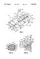
- FIG. 1is a simplified, somewhat schematic perspective view of an ink jet printhead structure, and associated high density remote driver interconnect apparatus, embodying principles of the present invention
- FIG. 2is an exploded perspective view of the printhead and interconnect apparatus
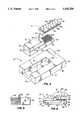
- FIG. 3is an enlarged scale partial cross-sectional view through the printhead taken along line 3--3 of FIG. 1;
- FIG. 4is a bottom plan view of the a multi-tiered printed circuit board portion of the interconnect apparatus
- FIG. 5is an enlarged scale perspective view of a corner portion of the multi-tiered circuit board showing, in highly schematic form, representative internal cross-over routings between high and low density side surface connector portions thereof;
- FIG. 6is a highly schematic side elevational view of the printhead illustrating the manner in which it may be operatively connected to a remotely mounted electronic driver.
- FIGS. 1 and 2Perspectively illustrated in FIGS. 1 and 2 is a specially designed ink jet printhead structure 10 embodying principles of the present invention and including a printhead 12, a mounting plate member 14, and a multi-tiered printed circuit board 16 used to electrically connect the printhead 12 to an electronic driver 18 (schematically depicted in FIG. 6) in a manner subsequently described.
- a left or front end section of the printhead 12is defined by a rectangular orifice plate 20 that is preferably formed from a nonpiezoelectric ceramic material. Extending rearwardly through the plate 20 are a horizontally spaced series of small ink discharge orifices 22. As illustrated, the orifices 22 are grouped in horizontally successive, vertically sloped sets.
- top and bottom body sections 24,26are substantially thicker than the intermediate body section 28, the widths of the three body sections are identical, the sections 24,28 rearwardly terminate in essentially the same vertical plane, and the bottom body section 26 extends rearwardly beyond the back ends of the sections 24,28 and has an exposed top side surface portion 30 and a rear end 32.
- the top and bottom body sections 24,26are preferably formed from a nonpolled ceramic material, although section 26 could be formed from a polled material if desired, and the vertically intermediate body section 28 is formed from a piezoelectrically active ceramic material suitably polled in a horizontal direction.
- a series of vertical grooves of predetermined width and depthare appropriately formed in the sections in a manner such that in the assembled printhead the grooves are horizontally aligned to form within the printhead body a horizontally spaced series of parallel interior channels 34.
- the horizontally spaced channels 34longitudinally extend rearwardly from the orifice plate 20, with the front end of each of the channels opening outwardly through one of the ink discharge orifices 22.
- Each of the channels 34is laterally bounded along its front-to-rear length by an opposed pair of a series of internal actuator sidewall sections 36.
- each actuator sidewall section 36is defined by vertically stacked portions of the printhead body sections 24,26,28.
- the channels 34communicate with an ink manifold chamber (not shown) formed within the interior of the printhead body.
- the manifold chamberis communicated with, and receives a supply of ink from, a suitable external ink supply vessel 38 (see FIG. 1) via a flexible ink delivery tube 40.
- the mounting plate member 14is preferably formed from a metal material, such as aluminum, and has a front end 40, a rear end 42, a top side 44 and a bottom side 46.
- An elongated, rectangularly cross-sectioned groove 48is formed in the top side 44 of the mounting plate member 14 and longitudinally extends rearwardly from its front end 40, the groove 48 having a rear end surface 50 spaced forwardly apart from the rear end 42 of the mounting plate member.
- the front-to-rear length of the groove 48is somewhat shorter than the corresponding length of the bottom printhead body section 26, the horizontal width of the groove 48 is just slightly greater than the corresponding width of the body section 26, and the vertical height of the groove 48 is essentially identical to that of the printhead body section 26.
- the bottom printhead body section 26is downwardly received, and suitably secured, within the groove 48 with the rear end 32 of body section 26 abutting the rear end surface 50 of the groove 48. Accordingly, the orifice plate 20 is forwardly spaced apart from the front end 40 of the mounting plate member 14, and the top side surface 30 (FIG. 2) of the bottom printhead body section 26 is essentially flush with the exposed top side surface 44 of the mounting plate member 14.
- the operative discharge of ink droplets from any selected one of the interior printhead body channels 34, via its associated orifice 22,is effected by imposing electrical driving voltages on the opposing actuator sidewall sections 36 (see FIG. 3) that bound such channel.
- these driving voltagesare transmitted to the actuator sidewall sections 36 (from the previously mentioned electronic driver 18 schematically shown in phantom in FIG. 6) via a series of mutually spaced, parallel electrically conductive surface traces 52 (see FIG. 2) formed on the exposed top side surface portion 30 of the bottom printhead body section 26.
- the parallel surface traces 52longitudinally extend in a front-to-rear direction along the exposed top side surface 30 of the bottom printhead body section 26, with the spaced apart front ends of the traces 52 being electrically connected to the similarly spaced segments of the piezoelectrically active printhead body section 28 that form vertically intermediate portions of the actuator sidewall sections 36.
- opposite polarity voltagesare transmitted, from the electronic driver 18 to the opposed actuator sidewall sections 36 that laterally bound the channel, through the appropriate pair of surface traces 52.
- Thiscauses the opposed pair of actuator sidewall actuator sections 36 to laterally deflect away from one another.
- the voltagesare then reversed which causes the sidewall actuator sections to deflect toward one another, thereby forcing ink in droplet form outwardly through the selected orifice 22.
- a ground potentialis applied to the sidewall actuator sections to cause them to return to their rest (i.e., undeflected) positions.
- the spacing between the parallel surface traces 52is also quite small, representatively on the order of about 3 mils.
- the connective interface formed on the printhead 12 by the surface traces 52is thus referred to as having a high density or pitch.
- the connective interface on the separate electronic driver 18(see FIG. 6) is of a considerably lower density (representatively on the order of about 50 mils) and is defined by a spaced series of electrically conductive surface pads 54a formed on the underside of a printed circuit board 56 forming a connection portion of the electronic driver 18.
- the operative connection between the high density surface traces 52 (FIG. 2) on the printhead 12 and the much lower density pads 54 on the driver circuit board 56 (FIG. 6)is releasably effected using the printed circuit board 16 (FIGS. 1 and 6) carried by the printhead 12.
- the printed circuit board 16has an elongated rectangular configuration, a front-to-rear length substantially longer than that of the exposed top side surface portion 30 of the printhead body section 26, a width substantially identical to that of the surface portion 30, a front end 58, and a rear end 60.
- Printed circuit board 16is of a multi-tier construction and, for purposes of illustration and discussion, is shown as representatively having, from top to bottom, three layers 16a,16b and 16c although it could have a much larger number of such layers.
- each of the traces 52abegins adjacent the front end 58 of the circuit board and ends a substantial distance forwardly of the rear end 60 of the circuit board 16.
- the trace sets 52,52amay be brought into precise registration with one another by placing a front underside portion of the circuit board 16 atop the exposed top side surface portion 30 of the printhead body section 26, in lateral alignment therewith, with the front end 58 of the circuit board 16 positioned against the rear end of the printhead body section 24.
- the top side of the upper circuit board layer 16ahas formed thereon a spaced series of electrically conductive surface pads 54a that have a pitch spacing (representatively about 50 mils) substantially greater than the pitch spacing of the linear surface traces 52,52a.
- the surface pads 54aare oriented on the circuit board layer 16a in a manner such that they may be brought into precise alignment with the surface pads 54 on the electronic driver circuit board 56.
- the surface pads 54aare positioned in a spaced apart orientation that extends over essentially the entire top side surface area of the circuit board 16.
- the surface pads 54a on the top side of the circuit board 16are operatively interconnected with the linear surface traces 52a on the bottom side of the circuit board 16 by means of a series of electrical crossover circuit paths 62 within the interior of the circuit board 16.
- the circuit paths 62representatively have horizontal portions 62a extending along the top side surfaces of the circuit board layers 16a,16b and 16c, and vertical "via" portions 62b extending vertically through such layers.
- the crossover paths 62constitute means for transitioning from the high density bottom side connection area defined by the linear traces 52a to the lower density top side connection area defined by the surface pads 54a, this expansion from high to low connection area densities taking place longitudinally along the printed circuit board 16.
- the printhead body section 26is placed in the mounting plate groove 48, and secured to the mounting plate member, as previously described.
- the circuit board 16is then placed atop the printhead body surface 30 and the top side 44 of the mounting plate member 14, as shown in FIG. 1, with the facing linear surface traces 52,52a in precisely registered contact with one another.
- the contacting surface trace sets 52,52aare then soldered to one another, preferably using a pressure/heat reflow process, thereby electrically connecting the surface traces 52 to the top side surface pads 54a.
- an electrically conductive adhesive materialcould be used to electrically connect the trace sets 52,52a to one another.
- the printhead structure 10may then be operably and releasably connected to the separate electronic driver 18 (see FIG. 6) simply by appropriately bringing the printhead structure surface pads 54a into releasable contact with the identically arranged contact pads 54 on the driver circuit board 56 as indicated by the double-ended arrow 64 in FIG. 6.
- the use of the multi-tiered printed circuit board 16 to effect the necessary high density-to-low density connection interface between the printhead 12 and the electronic driver 18provides the printhead structure 10 with several advantages. First, because the driver 18 is separately mounted within the overall printer structure, and not permanently secured to the printhead, the overall fabrication cost of the printhead 12, and thus its replacement cost, is substantially reduced.
- the use of the multi-tiered printed circuit board 16further reduces the overall fabrication cost of the printhead 12.
- the horizontal width of the array of linear surface traces 52 on the printhead bodyis only slightly less than the horizontal width of the printhead body. Accordingly, if a flexible ribbon connector was used to provide a high density-to-low density connection interface between the printhead and its associated electronic driver, the low density end of the ribbon connector would have to be considerably wider than the printhead body since the only direction for pitch expansion on the flexible ribbon connector would be along its width.
- the width of this interconnect portion of the printhead structureneed not exceed the width of the printhead body.
- the maximum width of the printheadis correspondingly reduced. This permits several printheads to be grouped in a close side-by-side relationship if desired.
- the use of the multi-tiered printed circuit board 16provides the printhead 12 with a more rugged construction and facilitates the connection of the printhead to its associated driver.
- the mounting plate member 14, which underlies a rear end portion of the circuit board 16serves not only to conveniently support the printhead 12 and facilitate its handling, but also functions to brace the circuit board 16 when it is operatively pressed into contact with the driver circuit board 56.
Landscapes
- Particle Formation And Scattering Control In Inkjet Printers (AREA)
- Ink Jet (AREA)
Abstract
Description
Claims (8)
Priority Applications (5)
| Application Number | Priority Date | Filing Date | Title |
|---|---|---|---|
| US08/020,050US5345256A (en) | 1993-02-19 | 1993-02-19 | High density interconnect apparatus for an ink jet printhead |
| CA002115893ACA2115893A1 (en) | 1993-02-19 | 1994-02-17 | High density interconnect apparatus for an inkjet printhead |
| AT94301186TATE152046T1 (en) | 1993-02-19 | 1994-02-18 | HIGH DENSITY CONNECTION ARRANGEMENT FOR INKJET PRINTHEAD |
| DE69402738TDE69402738T2 (en) | 1993-02-19 | 1994-02-18 | High density connector assembly for ink jet printhead |
| EP94301186AEP0611653B1 (en) | 1993-02-19 | 1994-02-18 | High density interconnect apparatus for an ink-jet printhead |
Applications Claiming Priority (1)
| Application Number | Priority Date | Filing Date | Title |
|---|---|---|---|
| US08/020,050US5345256A (en) | 1993-02-19 | 1993-02-19 | High density interconnect apparatus for an ink jet printhead |
Publications (1)
| Publication Number | Publication Date |
|---|---|
| US5345256Atrue US5345256A (en) | 1994-09-06 |
Family
ID=21796477
Family Applications (1)
| Application Number | Title | Priority Date | Filing Date |
|---|---|---|---|
| US08/020,050Expired - LifetimeUS5345256A (en) | 1993-02-19 | 1993-02-19 | High density interconnect apparatus for an ink jet printhead |
Country Status (5)
| Country | Link |
|---|---|
| US (1) | US5345256A (en) |
| EP (1) | EP0611653B1 (en) |
| AT (1) | ATE152046T1 (en) |
| CA (1) | CA2115893A1 (en) |
| DE (1) | DE69402738T2 (en) |
Cited By (18)
| Publication number | Priority date | Publication date | Assignee | Title |
|---|---|---|---|---|
| US5688391A (en)* | 1996-03-26 | 1997-11-18 | Microfab Technologies, Inc. | Method for electro-deposition passivation of ink channels in ink jet printhead |
| US5707684A (en)* | 1994-02-28 | 1998-01-13 | Microfab Technologies, Inc. | Method for producing micro-optical components |
| US5757404A (en)* | 1994-10-14 | 1998-05-26 | Oce-Nederland, B.V. | Inkjet array and method of production |
| US5984447A (en)* | 1995-05-10 | 1999-11-16 | Brother Kogyo Kabushiki Kaisha | L-shaped inkjet print head in which driving voltage is directly applied to driving electrodes |
| US6024439A (en)* | 1995-09-21 | 2000-02-15 | Canon Kabushiki Kaisha | Ink-jet head having projecting portion |
| US6188416B1 (en) | 1997-02-13 | 2001-02-13 | Microfab Technologies, Inc. | Orifice array for high density ink jet printhead |
| US6188414B1 (en) | 1998-04-30 | 2001-02-13 | Hewlett-Packard Company | Inkjet printhead with preformed substrate |
| US6328423B1 (en) | 1999-08-16 | 2001-12-11 | Hewlett-Packard Company | Ink jet cartridge with integrated circuitry |
| US20020109757A1 (en)* | 1999-02-09 | 2002-08-15 | Toshiba Tec Kabushiki Kaisha | Ink jet printer head and method for fabricating the same |
| US20020140954A1 (en)* | 2001-03-27 | 2002-10-03 | Kia Silverbrook | Printer assembly having flexible ink channel extrusion |
| US6642068B1 (en) | 2002-05-03 | 2003-11-04 | Donald J. Hayes | Method for producing a fiber optic switch |
| US6805902B1 (en) | 2000-02-28 | 2004-10-19 | Microfab Technologies, Inc. | Precision micro-optical elements and the method of making precision micro-optical elements |
| US20070153059A1 (en)* | 2004-01-21 | 2007-07-05 | Silverbrook Research Pty Ltd | Inkjet printhead having independent modular components |
| US20080311771A1 (en)* | 2007-06-12 | 2008-12-18 | Seong Bean Cho | Edge connection structure for printed circuit boards |
| US20100223975A1 (en)* | 2008-03-03 | 2010-09-09 | Keith Lueck | Calibration and Accuracy Check System for a Breath Tester |
| US20110273497A1 (en)* | 2010-05-10 | 2011-11-10 | Canon Kabushiki Kaisha | Recording head |
| JP2017056697A (en)* | 2015-09-18 | 2017-03-23 | コニカミノルタ株式会社 | Piezoelectric actuator unit, ink jet head, ink jet recording device, head chip and wiring substrate |
| JP2017109388A (en)* | 2015-12-16 | 2017-06-22 | エスアイアイ・プリンテック株式会社 | Liquid ejecting head and liquid ejecting apparatus |
Families Citing this family (2)
| Publication number | Priority date | Publication date | Assignee | Title |
|---|---|---|---|---|
| AUPQ455999A0 (en)* | 1999-12-09 | 2000-01-06 | Silverbrook Research Pty Ltd | Memjet four color modular print head packaging |
| US6585352B1 (en) | 2000-08-16 | 2003-07-01 | Hewlett-Packard Development Company, L.P. | Compact high-performance, high-density ink jet printhead |
Citations (3)
| Publication number | Priority date | Publication date | Assignee | Title |
|---|---|---|---|---|
| EP0183936A1 (en)* | 1984-11-28 | 1986-06-11 | Contraves Ag | Multilayer circuit and method of making the electrical connections |
| US4628332A (en)* | 1984-01-30 | 1986-12-09 | Canon Kabushiki Kaisha | Ink printhead with holder mount |
| US5227813A (en)* | 1991-08-16 | 1993-07-13 | Compaq Computer Corporation | Sidewall actuator for a high density ink jet printhead |
Family Cites Families (6)
| Publication number | Priority date | Publication date | Assignee | Title |
|---|---|---|---|---|
| US4879568A (en)* | 1987-01-10 | 1989-11-07 | Am International, Inc. | Droplet deposition apparatus |
| US4878070A (en)* | 1988-10-17 | 1989-10-31 | Xerox Corporation | Thermal ink jet print cartridge assembly |
| EP0468995B1 (en)* | 1989-04-17 | 1995-06-14 | Domino Printing Sciences Plc | Ink jet nozzle/valve, pen and printer |
| JPH03143644A (en)* | 1989-10-31 | 1991-06-19 | Sony Corp | Electrostatic recording head |
| JPH03153365A (en)* | 1989-11-13 | 1991-07-01 | Tokyo Electric Co Ltd | Thermal head |
| US5103246A (en)* | 1989-12-11 | 1992-04-07 | Hewlett-Packard Company | X-Y multiplex drive circuit and associated ink feed connection for maximizing packing density on thermal ink jet (TIJ) printheads |
- 1993
- 1993-02-19USUS08/020,050patent/US5345256A/ennot_activeExpired - Lifetime
- 1994
- 1994-02-17CACA002115893Apatent/CA2115893A1/ennot_activeAbandoned
- 1994-02-18ATAT94301186Tpatent/ATE152046T1/ennot_activeIP Right Cessation
- 1994-02-18DEDE69402738Tpatent/DE69402738T2/ennot_activeExpired - Fee Related
- 1994-02-18EPEP94301186Apatent/EP0611653B1/ennot_activeExpired - Lifetime
Patent Citations (3)
| Publication number | Priority date | Publication date | Assignee | Title |
|---|---|---|---|---|
| US4628332A (en)* | 1984-01-30 | 1986-12-09 | Canon Kabushiki Kaisha | Ink printhead with holder mount |
| EP0183936A1 (en)* | 1984-11-28 | 1986-06-11 | Contraves Ag | Multilayer circuit and method of making the electrical connections |
| US5227813A (en)* | 1991-08-16 | 1993-07-13 | Compaq Computer Corporation | Sidewall actuator for a high density ink jet printhead |
Cited By (41)
| Publication number | Priority date | Publication date | Assignee | Title |
|---|---|---|---|---|
| US5707684A (en)* | 1994-02-28 | 1998-01-13 | Microfab Technologies, Inc. | Method for producing micro-optical components |
| US5757404A (en)* | 1994-10-14 | 1998-05-26 | Oce-Nederland, B.V. | Inkjet array and method of production |
| US5984447A (en)* | 1995-05-10 | 1999-11-16 | Brother Kogyo Kabushiki Kaisha | L-shaped inkjet print head in which driving voltage is directly applied to driving electrodes |
| US6024439A (en)* | 1995-09-21 | 2000-02-15 | Canon Kabushiki Kaisha | Ink-jet head having projecting portion |
| US5858190A (en)* | 1996-03-26 | 1999-01-12 | Microfab Technologies, Inc. | Method for electro-deposition passivation of ink channels in ink jet printhead |
| US5688391A (en)* | 1996-03-26 | 1997-11-18 | Microfab Technologies, Inc. | Method for electro-deposition passivation of ink channels in ink jet printhead |
| US6188416B1 (en) | 1997-02-13 | 2001-02-13 | Microfab Technologies, Inc. | Orifice array for high density ink jet printhead |
| US6188414B1 (en) | 1998-04-30 | 2001-02-13 | Hewlett-Packard Company | Inkjet printhead with preformed substrate |
| US20020109757A1 (en)* | 1999-02-09 | 2002-08-15 | Toshiba Tec Kabushiki Kaisha | Ink jet printer head and method for fabricating the same |
| US7108359B2 (en)* | 1999-02-09 | 2006-09-19 | Toshiba Tec Kabushiki Kaisha | Ink jet printer head and method for fabricating the same |
| US6328423B1 (en) | 1999-08-16 | 2001-12-11 | Hewlett-Packard Company | Ink jet cartridge with integrated circuitry |
| US6805902B1 (en) | 2000-02-28 | 2004-10-19 | Microfab Technologies, Inc. | Precision micro-optical elements and the method of making precision micro-optical elements |
| US7914120B2 (en) | 2001-03-27 | 2011-03-29 | Silverbrook Research Pty Ltd | Modular printhead incorporating a capping device |
| US8070275B2 (en) | 2001-03-27 | 2011-12-06 | Silverbrook Research Pty Ltd | Method for assembling a modular printhead assembly |
| US8020966B2 (en) | 2001-03-27 | 2011-09-20 | Silverbrook Research Pty Ltd | Ink channel extrusion module for pagewidth printhead |
| US20070200897A1 (en)* | 2001-03-27 | 2007-08-30 | Silverbrook Research Pty Ltd | Method For Assembling A Modular Printhead Assembly |
| US7280247B2 (en)* | 2001-03-27 | 2007-10-09 | Silverbrook Research Pty Ltd | Printer assembly having flexible ink channel extrusion |
| US20070263047A1 (en)* | 2001-03-27 | 2007-11-15 | Silverbrook Research Pty Ltd | Printhead Ink Delivery System With Clamping Endcap |
| US7303256B2 (en) | 2001-03-27 | 2007-12-04 | Silverbrook Research Pty Ltd | Printhead assembly comprised of a plurality of printhead modules |
| US20070296762A1 (en)* | 2001-03-27 | 2007-12-27 | Silverbrook Research Pty Ltd | Modular printhead incorporating a capping device |
| US20110134189A1 (en)* | 2001-03-27 | 2011-06-09 | Silverbrook Research Pty Ltd | Inkjet printer having modular pagewidth printhead |
| US20020140954A1 (en)* | 2001-03-27 | 2002-10-03 | Kia Silverbrook | Printer assembly having flexible ink channel extrusion |
| US20100214363A1 (en)* | 2001-03-27 | 2010-08-26 | Silverbrook Research Pty Ltd | Method for assembling a modular printhead assembly |
| US7775640B2 (en) | 2001-03-27 | 2010-08-17 | Silverbrook Research Pty Ltd | Printhead ink delivery system with clamping endcap |
| US7581814B2 (en) | 2001-03-27 | 2009-09-01 | Silverbrook Research Pty Ltd | Ink channel extrusion module for a pagewidth printhead |
| US20090295883A1 (en)* | 2001-03-27 | 2009-12-03 | Silverbrook Research Pty Ltd | Ink Channel Extrusion Module For Pagewidth Printhead |
| US7712866B2 (en) | 2001-03-27 | 2010-05-11 | Silverbrook Research Pty Ltd | Method for assembling a modular printhead assembly |
| US6642068B1 (en) | 2002-05-03 | 2003-11-04 | Donald J. Hayes | Method for producing a fiber optic switch |
| US20080246812A1 (en)* | 2004-01-21 | 2008-10-09 | Silverbrook Research Pty Ltd | Printer Assembly For A Pagewidth Printer Having A Support Frame Configured To Minimize Substantial Dimensional Changes |
| US7399053B2 (en)* | 2004-01-21 | 2008-07-15 | Silverbrook Research Pty Ltd | Inkjet printhead having independent modular components |
| US20070153059A1 (en)* | 2004-01-21 | 2007-07-05 | Silverbrook Research Pty Ltd | Inkjet printhead having independent modular components |
| US8100509B2 (en) | 2004-01-21 | 2012-01-24 | Silverbrook Research Pty Ltd | Printer assembly for a pagewidth printer having a support frame configured to minimize substantial dimensional changes |
| US20080311771A1 (en)* | 2007-06-12 | 2008-12-18 | Seong Bean Cho | Edge connection structure for printed circuit boards |
| US7534966B2 (en)* | 2007-06-12 | 2009-05-19 | Clear Electronics, Inc. | Edge connection structure for printed circuit boards |
| US8418523B2 (en) | 2008-03-03 | 2013-04-16 | Keith Lueck | Calibration and accuracy check system for a breath tester |
| US20100223975A1 (en)* | 2008-03-03 | 2010-09-09 | Keith Lueck | Calibration and Accuracy Check System for a Breath Tester |
| US8713985B2 (en) | 2008-03-03 | 2014-05-06 | Alcotek, Inc. | Calibration and accuracy check system |
| US20110273497A1 (en)* | 2010-05-10 | 2011-11-10 | Canon Kabushiki Kaisha | Recording head |
| US9186897B2 (en)* | 2010-05-10 | 2015-11-17 | Canon Kabushiki Kaisha | Recording head |
| JP2017056697A (en)* | 2015-09-18 | 2017-03-23 | コニカミノルタ株式会社 | Piezoelectric actuator unit, ink jet head, ink jet recording device, head chip and wiring substrate |
| JP2017109388A (en)* | 2015-12-16 | 2017-06-22 | エスアイアイ・プリンテック株式会社 | Liquid ejecting head and liquid ejecting apparatus |
Also Published As
| Publication number | Publication date |
|---|---|
| EP0611653B1 (en) | 1997-04-23 |
| ATE152046T1 (en) | 1997-05-15 |
| DE69402738D1 (en) | 1997-05-28 |
| EP0611653A3 (en) | 1994-09-14 |
| DE69402738T2 (en) | 1997-11-13 |
| CA2115893A1 (en) | 1994-08-20 |
| EP0611653A2 (en) | 1994-08-24 |
Similar Documents
| Publication | Publication Date | Title |
|---|---|---|
| US5345256A (en) | High density interconnect apparatus for an ink jet printhead | |
| JP3534762B2 (en) | INK JET PRINT HEAD DEVICE AND ITS MANUFACTURING METHOD | |
| JP5274741B2 (en) | Droplet adhesion device | |
| EP0615845A2 (en) | Methods of fabricating a page wide piezoelectric ink jet printhead assembly | |
| KR100556659B1 (en) | Ink printing device | |
| US7874651B2 (en) | Liquid droplet discharge head and liquid droplet discharge apparatus | |
| JPH02151445A (en) | Improved thermal-ink printing cartridge assembly | |
| US6682180B2 (en) | Ink jet head and printing apparatus | |
| US6281914B1 (en) | Ink jet-type printer device with printer head on circuit board | |
| US9566789B2 (en) | Liquid discharge apparatus and method for producing piezoelectric actuator | |
| US20060170738A1 (en) | Ink-Jet Head and Connecting Structure | |
| US7597426B2 (en) | Ink-jet head and ink-jet printer | |
| US6886914B2 (en) | Liquid jetting apparatus | |
| US6095641A (en) | Simplified ink jet recording head and a manufacturing method thereof | |
| US5444467A (en) | Differential drive system for an ink jet printhead | |
| EP0268395A2 (en) | Print head for ink jet printer | |
| US7441874B2 (en) | Insulated heat unit for ink jet printer, an ink jet printer including an insulated head unit and signal transmission board used for the ink jet printer | |
| EP1512534A1 (en) | Inkjet head | |
| US6979078B2 (en) | Ink-jet head with ink blockage prevention device | |
| US7156501B2 (en) | Inkjet head | |
| US7347522B2 (en) | Ink-jet head and image recording apparatus | |
| JP2005059337A (en) | Inkjet head and inkjet printer | |
| US20070229635A1 (en) | Ink-Jet Head | |
| US8136927B2 (en) | Liquid droplet discharge head, liquid droplet discharge apparatus, and method for producing liquid droplet discharge head | |
| US7219981B2 (en) | Ink-jet head and producing method thereof |
Legal Events
| Date | Code | Title | Description |
|---|---|---|---|
| AS | Assignment | Owner name:COMPAQ COMPUTER CORPORATION, TEXAS Free format text:ASSIGNMENT OF ASSIGNORS INTEREST.;ASSIGNOR:STORTZ, JAMES L.;REEL/FRAME:006496/0517 Effective date:19930204 | |
| STCF | Information on status: patent grant | Free format text:PATENTED CASE | |
| FPAY | Fee payment | Year of fee payment:4 | |
| AS | Assignment | Owner name:COMPAQ INFORMATION TECHNOLOGIES GROUP, L.P., TEXAS Free format text:ASSIGNMENT OF ASSIGNORS INTEREST;ASSIGNOR:COMPAQ COMPUTER CORPORATION;REEL/FRAME:012418/0222 Effective date:20010620 | |
| FPAY | Fee payment | Year of fee payment:8 | |
| AS | Assignment | Owner name:HEWLETT-PACKARD DEVELOPMENT COMPANY, L.P., TEXAS Free format text:CHANGE OF NAME;ASSIGNOR:COMPAQ INFORMATION TECHNOLOGIES GROUP, LP;REEL/FRAME:015000/0305 Effective date:20021001 | |
| FEPP | Fee payment procedure | Free format text:PAYOR NUMBER ASSIGNED (ORIGINAL EVENT CODE: ASPN); ENTITY STATUS OF PATENT OWNER: LARGE ENTITY | |
| FPAY | Fee payment | Year of fee payment:12 |