US5343406A - Distributed memory architecture for a configurable logic array and method for using distributed memory - Google Patents
Distributed memory architecture for a configurable logic array and method for using distributed memoryDownload PDFInfo
- Publication number
- US5343406A US5343406AUS07/387,566US38756689AUS5343406AUS 5343406 AUS5343406 AUS 5343406AUS 38756689 AUS38756689 AUS 38756689AUS 5343406 AUS5343406 AUS 5343406A
- Authority
- US
- United States
- Prior art keywords
- memory cells
- logic
- lines
- configurable logic
- array
- Prior art date
- Legal status (The legal status is an assumption and is not a legal conclusion. Google has not performed a legal analysis and makes no representation as to the accuracy of the status listed.)
- Expired - Lifetime
Links
Images


Classifications
- H—ELECTRICITY
- H03—ELECTRONIC CIRCUITRY
- H03K—PULSE TECHNIQUE
- H03K19/00—Logic circuits, i.e. having at least two inputs acting on one output; Inverting circuits
- H03K19/02—Logic circuits, i.e. having at least two inputs acting on one output; Inverting circuits using specified components
- H03K19/173—Logic circuits, i.e. having at least two inputs acting on one output; Inverting circuits using specified components using elementary logic circuits as components
- H03K19/1733—Controllable logic circuits
- H03K19/1735—Controllable logic circuits by wiring, e.g. uncommitted logic arrays
- H03K19/1736—Controllable logic circuits by wiring, e.g. uncommitted logic arrays in which the wiring can be modified
Definitions
- This inventionrelates to means and methods of performing custom logic functions in an integrated circuit logic device.
- a Xilinx configurable logic arrayincludes an array of logic blocks, each of which can be configured to perform a desired logic function (each logic block combining multiple AND, OR, MUX gates or FLIP-FLOPs for example).
- the Xilinx configurable logic arrayalso includes interconnect lines which can be programmed to connect individual logic blocks to achieve the overall complex logic function provided by the entire chip. In the current Xilinx products, two kinds of configurable blocks are used in a configurable logic array chip.
- input/output logic blockswhich can be programmed to connect input buffers or output buffers to the pin and to perform some logic functions.
- logic blockswhich do not offer the input/output buffer option but offer more logic functions within a single block.
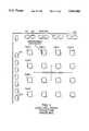
- FIG. 1shows part of one of the configurable logic array chips for which automatic programming is available.
- Configurable input/output blocks IO1 through IO15are shown.
- Configurable logic blocks CLB11-CLB14, CLB21-CLB24, CLB31-CLB34 and CLB41-CLB44are shown.
- Each of the configurable blocksimplements a plurality of logic gates such as AND, OR, XOR, INVERT, and MUX, as well as TRISTATE buffers and FLIPFLOP's which can be combined to implement a plurality of more complex logic functions.
- the logic gates of a logic blockare formed into flexible functions which are specified when the block is configured.
- the logic blockmay include a four-input AND gate. Zero, one two, three or four AND gate inputs need be used, the unused inputs being connected to the positive voltage supply. An input signal may pass directly or through an inverter to the AND gate. Since gates within a block are physically located and connected together in the substrate and adjoining layers of the semiconductor material, any desired one of a plurality of functions such as AND, OR, NAND, NOR, XOR of two inputs A and B can be performed by electronic components located in close physical proximity, therefore the signal delay caused by the logic block is minimal in spite of the flexibility and complexity of the logic block.
- One type of logic blockis programmed to provide a desired function of several input signals by loading memory cells of a look-up table with the truth table of a desired logic function. This way great flexibility is achieved with minimum signal delay.
- These configurable blockseach have input and output leads for receiving input signals and providing output signals. These leads are shown in FIG. 1 as short lines extending outward from each of the blocks and not connected to other portions of the array. These configurable blocks also have configuration leads not shown in FIG. 1 for programming the particular logic function or loading the truth table. The configuration leads determine what logic function will be applied by the block to signals entered on its input leads to generate a signal placed by the block on its output lead or leads. These logic blocks are discussed in U.S. Pat. No. 4,706,216 issued Nov. 10, 1987, which is incorporated herein by reference.
- FIG. 2shows in more detail a smaller portion of a configurable logic array chip with the interconnects lines for connecting one configurable logic block (CLB) or input/output block (IOB) to another CLB or IOB.
- CLBconfigurable logic block
- IOBinput/output block
- Some of the interconnect linesare short segments which extend only a short part of the distance across the entire array, and others typically extend in one dimension the entire length or width of the array.
- FIG. 2bis a legend showing meanings for the marks in FIG. 2a.
- Diagonal linesindicate programmable pass transistors for connecting horizontal lines to vertical lines. Each transistor will have one current carrying terminal connected to a horizontal line and one to a vertical line.
- FIG. 2ashows in more detail this full-exchange interconnection indicated by an "X" in FIG. 2a.
- Line 90-4is segmented from line 90-1 in that it is connected to line 90-1 by N-channel pass transistor T5 when memory cell M5 holds a logical 1 and disconnected from line 90-1 when memory cell M5 holds a logical 0.
- FIGS. 2a through 2dare discussed more full in U.S. patent application Ser. No. 07/158,011, now U.S. Pat. No. 4,870,302, incorporated herein by reference.
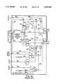
- FIG. 3ashows one possible CLB which is part of a configurable logic array and can be configured to perform many different logic functions.
- FIG. 3ashows combinatorial function generator 354 having input lines 381-385 for receiving logic block inputs a-3 and input lines 367 and 380 for receiving output signals from D-flipflops 352 and 357 respectively.
- Combinatorial function generator 354also provides two combinatorial output functions F and G on lines 374 and 378, each of which may serve as input to either or both flipflops 352 and 357 as controlled by multiplexers 350, 351, 355 and 356.
- Output functions F and Gmay also be provided as logic block output signals X and Y respectively on lines 395 and 396 as controlled by multiplexers 353 and 358.
- FIG. 3aWhich functions are actually implemented by the logic block of FIG. 3a depends upon the settings of configuration control lines not shown in FIG. 3a.
- configuration control linesare shown in FIG. 3b as lines extending from RAM 108 or 109 to select multiplexer 110 or 111.
- Combinatorial function generator 354 of FIG. 3agenerates two cominatorial functions F and G just as block 100 of FIG. 3b generates two combinatorial functions F1 and F2.
- FIG. 3bis discussed in U.S. Pat. No. 4,706,216, ibid.
- Combinatorial function generator 354can generate any combinatorial function of five variables, or can generate two functions of four variables each.
- combinatorial function generator 354is programmed by loading a truth table into a row of memory cells. As is well known, an n-input multiplexer can select one of 2 n locations in response to an n-bit address.
- Function generator 354is a multiplexer which reads one of 32 (2 5 ) memory cells in response to an address which comprises the five input signals on lines 381-385, or alternatively reads one of sixteen memory cells to provide a first function of four of the variables on a first output line, and reads one of a second sixteen memory cells to provide a second function of any four of the five variables on a second output line 378.
- the operation of the logic block of FIG. 3ais described more thoroughly in the Xilinx "Programmable Gate Array Data Book", copyright 1988 by Xilinx, Inc., available from Xilinx, Inc., 2100 Logic Drive, San Jose, Calif. 95124.
- a logic array including configurable blocks such as shown in FIG. 3a or 3b and interconnect lines such as shown in FIG. 2acan be configured to perform a multiplicity of complex logic functions. For example, it can be programmed to perform the function which is represented by the schematic diagram of FIG. 3c.
- the schematic of FIG. 3cincludes input buffers, logic gates AND1OUT, XOR1OUT, OR1OUT, and OR2OUT, flip flops Q1OUT and Q2OUT, and output buffers.
- the input and output buffersare provided by input/output blocks P2 through P9. These blocks are located at the periphery of the logic array chip.
- Gates AND1OUT and OR1OUT and flip flop Q1OUTare implemented in logic block AB; gate XOR1OUT and flip flop Q2OUT are implemented in logic block AC, and gate OR2OUT is implemented in logic block AA.
- Logic blocks AA, AB, and ACcan be of the type shown in FIG. 3b.
- FIG. 3bcan be configured to provide the Qff output signal of flip flop 121 as the Y output of the logic block.
- the logic block of FIG. 3bimplements the logic shown in block AB of FIG. 3d.
- other logic blocks of the type shown in FIG. 3bcan implement the logic shown in blocks AC and AA of FIG. 3d.
- memory cellshave been used in existing logic arrays to control the logic functions performed by the arrays by writing values to the memory cells such as 8-bit RAM 109 of FIG. 3b during a configuration step, these memory cells have not been accessible to a user of the logic array for writing, storing, and reading data during operation of the logic array, as will now be explained.
- the prior art memory cell of FIG. 4comprises two inverters 41 and 42 connected in a loop such that the input of one inverter is connected to the output of the other inverter.
- Data line (or bit line) Dyis connected to or disconnected from the inverter by address line (or word line) Ax.
- Either output line Q or its inverse Qcontrols the state of one of the configuration transistors in a logic block such as shown in FIG. 3a or 3b.
- a preferred embodiment of this prior art memory cellachieves a known state on power-up and is described in U.S. Pat. No. 4,821,233 issued Apr. 11, 1989, incorporated herein by reference.
- the memory cell of FIG. 4is loaded during configuration of the array.
- This configuration steprequires that certain of the pins at the external perimeter of the array be used for configuration signals. When configuration is complete, these same external pins are most frequently configured to serve as data input or output pins. One or two pins have been used to switch the chip from configuration to operation mode but no provision has been available to alter these memory cells during operation after the configuration step is complete. Memory needed by a user during operation of such an array has generally been provided on a separate chip.
- memorydistributed within the logic array, and to have the distributed memory available for access by the user during operation of the array.
- the userintends to use a configurable logic array chip as a combination central processing unit, a memory, and a first-in-first-out output buffer
- the present inventionprovides means and method for programming a configurable logic block so that some of the configuration memory cells of the block can be changed during operation and may be used as a RAM (random access memory) for storing data of the user as well as for generating a logic function.
- the same logic blockcan be reconfigured so that at another time the memory cells which were once under control of the user during operation are configured to provide a static logic function which does not change during operation.
- the present inventionoffers flexibility not only in how certain memory cells are used but also in where within the logic array the user-accessible data cells are placed.
- the memory cells which may alternatively be used for storing dataare those which store the lookup table used for configuring a combinatorial logic function which is within a logic block.
- Other memory cellsmay be used only for their configuration function and not alternatively for storing data, for example those which control the interconnection between logic blocks.
- the MUX memory cells which control connection of flip flops to other elements within a logic blockmay be alternatively used for data in one embodiment, though in a presently preferred embodiment these MUX internal configuration cells are used for configuration only.
- MUX internal configuration cellsalternatively for memory in an embodiment in which there are relatively few MUX configuration cells and the MUX configuration cells are not grouped in groups of eight such that they could be conveniently dedicated to storing at least a byte of information.
- To use the MUX cells for storagewould result in a relatively inefficient use of the powerful logic options available with the preferred embodiment, therefore address lines necessary for such use are not presently provided.
- This optionis provided by including two means for accessing each dual function cell, one which is used to supply off-chip signals during configuration of the cell and another which is used during operation to store signals which may be generated on-chip.
- FIG. 1shows part of one of the configurable logic array chips for which automatic programming is available.
- FIG. 2(A through D) show a small portion of a configurable logic array chip with interconnects for connecting leads of one CLB or IOB to another CLB or IOB.
- FIG. 3ashows one prior art configurable logic block.
- FIG. 3bshows another prior art configurable logic block in which memory cells for storing the configuration of the combinatorial logic functions are shown.
- FIG. 3cshows a representative logic function which can be implemented by two logic blocks of the type shown in FIG. 3b.
- FIG. 3dshows the portions of logic which will be implemented by each of the logic blocks.
- FIG. 4shows a prior art 5-transistor memory cell of a type which can be used to configure the configurable logic blocks of FIG. 3a or 3b.
- FIG. 5ashows a configurable logic block incorporating the present invention.
- FIG. 5bshows a portion of a configurable logic array incorporating the logic block of FIG. 5a.
- FIG. 6shows a 5-transistor memory cell having dual access means for use with the present invention.
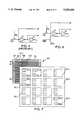
- FIG. 7shows a schematic representation of a logic array chip having logic blocks, each logic block providing two logic functions under control of a configuration memory array.
- FIG. 8shows part of one circuit for providing the distributed memory cells of FIG. 6 in the logic block of FIG. 5a.
- FIG. 7illustrates a logic array chip having 16 logic blocks.
- the principles discussed herewill of course apply to a chip having any number of logic blocks.
- the logic blocks shown in FIG. 7are identical, that is, they can all be programmed to perform the same functions. (Once they have been configured, each logic block performs a specific function as specified by the user, typically not identical to that of other logic blocks. Interconnect lines can provide outputs from one logic block as input to another logic block, again as specified by the user.
- the blocks in an arrayare generally not configured identically.
- some of the blocks in an arraymay serve as memory devices rather than function generators.
- the usercan build a logic system which contains combinatorial logic, flip-flops for logic storage, and groups of memory cells for data storage.
- FIG. 7includes a grid M7 of memory cells for configuring the sixteen logic blocks B1,1 through B4,4.
- Address lines A1 through A32run horizontally and data lines D1 through D32 run vertically through grid M7.
- Ax and Dydenote representative address and data lines respectively.
- a memory cellis located at each intersection of the grid of FIG. 7.
- the group of memory cells C1,1comprises a lookup table for the configuration of function generators F1,1 and G1,1 in block B1,1.
- the memory cells at the intersections of address line A1 through A4 and data lines D1 through D4store the lookup table for the function generator F1,1 and each of them may be formed as shown in FIG. 6.
- the memory cells at the intersection of address lines A5 through A8 and data lines D1 through D4store the lookup table for the function generator G1,1.
- Memory cells at the intersections of address lines A1 through A8 with data lines D5 through D8store configuration information for other parts of the block B1,1 not part of the combinational function generators F1,1 and G1,1. These memory cells may be formed as shown in FIG. 4. Memory cells for the other blocks in FIG. 7 follow the same pattern.
- the combinatorial logic table memory cells at the intersection of address lines A1 through A32 and data lines D1-D4, D9-D12, D17-D20, and D25-D28have the dual control shown in FIG. 6 so that they may be loaded during configuration of the chip by applying data on lines D1-D4, D9-D12, D17-D20, and D25-D28 while accessing cells through address lines A1 through A32, then loaded (written to) or read by other logic on the chip at any time during operation of the logic array as will be discussed below.
- Other memory cellspreferably have the single access shown in FIG. 4.
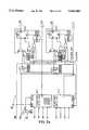
- FIG. 5ashows a generalized one of the logic blocks Bj,k of FIG. 7 in more detail.
- FIG. 5bshows the configurable logic block of FIG. 5a surrounded by interconnect structure which is also part of the configurable logic array of FIG. 7. Reference numerals in FIG. 5b which are the same as those in FIG. 5a have the same meaning as they have in FIG. 5a.
- function generator F1,1is a multiplexer which reads one of sixteen memory cells (shown in FIG. 7 as at the intersections of address lines A1 through A4 and data lines D1 through D4 but not shown in FIG. 54) in response to an address provided on four input lines F1, F2, F3 and F4.
- the memory cell contentsit is possible to read the memory cell contents during operation as well as to use the memory cell contents to control a logical operation performed by the logic block in which the memory cells reside.
- the usercan write new data into the memory cells and he can then perform the new function represented by the new data or read the data out for use elsewhere in the logic array. Data can be changed one table at a time, under control of the logic programmed into the array.
- the architectureis more flexible and more efficient because the same memory cells can be used for more than one purpose. Since in a preferred embodiment, logic blocks have the same architecture throughout the array, the distributed memory provided by this invention can be used where needed.
- the memory cells of this inventioncan be used as a RAM. If the user wants a byte-wide register set with 16 bytes of registers, he can program 8 function blocks to be loaded as a RAM, and control these 8 function blocks as a register. Similarly, if the user needs a 256 by 1 bit organization, the outputs of function blocks (each with 32 bits) are multiplexed together to form the required organization by configuring appropriate memory cells during configuration of the array.
- the circuit of FIG. 5aincorporates the two means for accessing memory cells such as shown in FIG. 6.
- Write enable line WEcan be controlled by a user during operation of the cell to allow for loading data on line DIN into function generator F1,1 or on one of lines DIN or H1 through line Du into function generator G1,1.
- line DINcan be used when the write enable line is high (function generators F1,1 and G1,1 are not being loaded) to provide data to flip flops FF1 and/or FF2 if memory cells M2 through M13 are programmed so that data on line DIN is received on the D input port of flip flops FF1 and/or FF2.
- FIG. 8The dual means for controlling the memory cell of FIG. 6 as used in the function generators F1,1 and G1,1 of FIG. 5a will now be explained.
- the operation of function generators F1,1 and G1,1is shown in more detail in FIG. 8.
- Function generator inputs F1 through F4 shown in FIG. 5aare shown in FIG. 8 as selected from among a plurality of signals. In one embodiment, 18 lines are provided from which to select the F4 input signal. Many variations and means for selecting from a plurality of signals are possible.
- FIG. 5bshows 16 lines from which the F1 signal is taken and 14 from which the F4 signal is taken, each line separately controlled by a memory cell.
- the variation shown in FIG. 8provides for selecting the signal from only one of 18 lines by a two step selection process.
- the signal on each of these 18 linesis buffered through a buffer such as B81.
- the signalsare grouped into three groups of five and one group of three signals.
- Pass transistors such as transistor M81are controlled by a multiplexer to select one signal of each group of signals and pass transistors such as transistor M82 are controlled by this multiplexer to select one of the groups of signals, such that a single signal from the 18 lines is presented as the F4 signal.
- This F4 signalis inverted by inverter I81 and provided as input to NOR gates NOR81 and NOR82.
- the signalis inverted again by inverter I82 and provided as input to NOR gates NOR83 and NOR84.
- a similar operationgenerates function F2 which is inverted by inverter I83 and provided as input to NOR gates NOR82 and NOR84, and inverted again by inverter I84 and provided to NOR gates NOR81 and NOR83.
- function F2which is inverted by inverter I83 and provided as input to NOR gates NOR82 and NOR84, and inverted again by inverter I84 and provided to NOR gates NOR81 and NOR83.
- a plurality of memory cellseach provide bits of a word stored in function generator F1,1.
- Each of the memory cellssuch as memory cells M1,1 and M1,2 are formed as illustrated in FIG. 6.
- the lines for configuring memory cells M1,1 and M1,2 during the process of configuring the entire logic arrayare labeled Dy1 and Dy2 respectively, and their respective address lines are labeled Ax1 and Ax2.
- memory cells M1,1 and M1,2may be configured by data applied under control of the same address line, Ax1 for example.
- memory cell WE-Fwill be loaded with a logical zero during configuration, thereby providing a logical one to NOR gate NORFH1 and enabling NOR gate NORFH1 to respond to a write enable signal on line WE if NOR gate NORFH1 is also enabled by AND gate ANDFH1.
- FIG. 8does not show the memory cells of the G function generator G1,1, nor does it show means for addressing the memory cells of the G function generator.
- the memory cells of the G function generator F1,1are addressed, read, and written by circuitry which is identical to that for addressing the F function generator except for the following differences which are shown in FIG. 8.
- the signal H1is provided to AND gate ANDFH1 and its complement H1 is provided to AND gate ANDGH1.
- Multiplexer MUX 51selects which of signals DIN and H1 are provided to the G function generator. If signal DIN is provided to the G function generator, only one of the F function generator and the G function generator will be addressed at one time, since H1 and H1 are complementary signals.
- the single data line DINcan be used for providing data to memory cells in both F function generator F1,1 and G function generator G1,1.
- the embodiment discussed in detail hereuses 16 memory cells in each of function generators F1,1 and G1,1, and uses four input lines to address each of these sets of memory cells. It is clear that the invention is not limited to this embodiment, since other numbers of memory cells and address lines, for example 128 memory cells and six address lines, could also be used. Further, a logic block need not be limited to providing two functions.
- FIG. 8there are sixteen memory cells, M1,1 through M1,16 in function generator F1,1 of which only two are shown. Control of the remaining memory cells can be understood from the level of detail shown in FIG. 8.
- Memory cell M1enables both AND gate ANDFH1 and AND gate ANDGH1 and determines whether the logic block of FIG. 5a will treat the 32 memory cells in function generators F1,1 and G1,1 as a single bank of 32 cells for which a single output is selected in response to signals on the eight lines F1 through F4 and G1 through G4, or whether the logic block of FIG.
- a logical 1 in memory cell M1produces a logical 0 on the inverted output of memory cell M1, turning off transistor T51b of MUX 51 and disabling the H1 and H1 inputs to AND gates ANDFH1 and ANDGH1 respectively.
- the logical 1 in memory cell M1turns on transistor T51a in MUX 51, which allows the signals on line H1 to be used as data signals to function generator G1,1.
- a logical 0 in memory cell M1turns off transistor T51a so that the signals on line H1 are not provided as data to G function generator G1,1.
- the high signal provided on the inverted output of memory cell M1turns on transistor T51b, causing the G function generator G1,1 to receive data on line DIN.
- This high signal on the inverted output of memory cell M1is also provided to AND gates ANDFH1 and ANDGH1, enabling the signal on lines H1 and H1 to be provided to NOR gates NORFH1 and NORGH1 respectively.
- NOR gates NORFH1 and NORGH1As can be seen in FIG. 8, a logical 1 in memory cell WE-F produces a logical 0 to NOR gate NORFH1.
- Only one of memory cells M1,1 through M1,16will be connected at any one time to line DIN by having all three of its write enable transistors such as T85,1, T81a and T81H turned on.
- the decodingis performed in two stages (other decode logic is also possible, as is well known).
- Writing to memory cells M1,1 through M1,4is controlled by NOR gate NOR85 which provides a high output signal only when lines F1 and F3 are low.
- Three other groups of memory cells M5 through M16(not shown) are addressed by other combinations of signals on lines F1 and F3.
- transistors T85,1 through T85,4will be high. If lines F2 and F4 are low, NOR gate NOR81 will provide a high output signal (and NOR gates NOR82 through NOR84 will all provide low output signals). The high output signal on NOR gate NOR81 will turn on transistors T81a and T81b. If transistor T81H is also on, the data on line DIN as inverted by inverter IIN will be written to memory cell M1,1.
- transistors T81b and T85bare also turned on by the combination of low signals on lines F1 through F4, the data on DIN which is inverted and entered to memory cell M1,1 will be inverted again by inverter I1,1 and provided on F function generator output line FA.
- inverter I1,1it is possible to provide the Q output of memory cell M1,1 to the output line FA of function generator F1,1.
- inverters I1,1, I1,2, etcit is possible to provide a single inverter to invert and buffer the signal on node N85.
- such an embodimentis not preferred because signal propagation would be slower.
- memory cells M1 through M16are configured as RAM storage, in the embodiment of FIG. 8, they will be read as serial output on the FA output line from F function generator F1,1.
- the F output signal from function generator F1,1 shown in FIG. 5ais derived by providing the FA output signal of FIG. 8 to an inverter. This data is accessed by connecting, during configuration of the array, the F output line shown in FIG. 5b to a desired input line of another configurable logic block like that shown in FIG. 5b located in another part of the array.
- the four signals H1, DIN, WE and clock enable signal CEcan be taken from interconnect lines physically spaced apart around the logic block. In one embodiment these signals are decoded within the logic block and applied to desired lines, adding another level of programmability.
Landscapes
- Physics & Mathematics (AREA)
- Engineering & Computer Science (AREA)
- Computer Hardware Design (AREA)
- Computing Systems (AREA)
- General Engineering & Computer Science (AREA)
- Mathematical Physics (AREA)
- Logic Circuits (AREA)
Abstract
Description
This invention relates to means and methods of performing custom logic functions in an integrated circuit logic device.
As integrated circuit devices have become able to perform more functions within a single integrated circuit chip, the manufacturers of integrated circuit chips have developed ways of automatically and quickly responding to orders for custom chips to perform specific functions for specific applications. On the one hand, gate array manufacturers apply custom metallization layers as a final step in a standard manufacturing process in order to connect transistors located within a semiconductor substrate to perform a particular logic function ordered by a customer. On the other hand, for customers who make frequent design changes, who want only small numbers of identical devices, or who may not have fully tested a new design, user programmable integrated circuit chips are available. In a user programmable device, there are many pass transistors which can be turned on or off to connect or not connect corresponding lines to logic circuits, to other lines, or output pins. By turning on the proper combination of pass transistors and connecting the proper set of lines a user can obtain a desired logic function. The user can reprogram a different design into the chip by turning on different combinations of pass transistors.
Xilinx, Inc. the assignee of the present invention, manufactures configurable logic arrays having a higher level of integration than typical programmable logic arrays. A Xilinx configurable logic array includes an array of logic blocks, each of which can be configured to perform a desired logic function (each logic block combining multiple AND, OR, MUX gates or FLIP-FLOPs for example). The Xilinx configurable logic array also includes interconnect lines which can be programmed to connect individual logic blocks to achieve the overall complex logic function provided by the entire chip. In the current Xilinx products, two kinds of configurable blocks are used in a configurable logic array chip. Around the perimeter of the chip, and connected to each of the external pins are input/output logic blocks which can be programmed to connect input buffers or output buffers to the pin and to perform some logic functions. In the interior of the chip are logic blocks which do not offer the input/output buffer option but offer more logic functions within a single block.
FIG. 1 shows part of one of the configurable logic array chips for which automatic programming is available. Configurable input/output blocks IO1 through IO15 are shown. Configurable logic blocks CLB11-CLB14, CLB21-CLB24, CLB31-CLB34 and CLB41-CLB44 are shown. Each of the configurable blocks implements a plurality of logic gates such as AND, OR, XOR, INVERT, and MUX, as well as TRISTATE buffers and FLIPFLOP's which can be combined to implement a plurality of more complex logic functions.
The logic gates of a logic block are formed into flexible functions which are specified when the block is configured. For example the logic block may include a four-input AND gate. Zero, one two, three or four AND gate inputs need be used, the unused inputs being connected to the positive voltage supply. An input signal may pass directly or through an inverter to the AND gate. Since gates within a block are physically located and connected together in the substrate and adjoining layers of the semiconductor material, any desired one of a plurality of functions such as AND, OR, NAND, NOR, XOR of two inputs A and B can be performed by electronic components located in close physical proximity, therefore the signal delay caused by the logic block is minimal in spite of the flexibility and complexity of the logic block. One type of logic block is programmed to provide a desired function of several input signals by loading memory cells of a look-up table with the truth table of a desired logic function. This way great flexibility is achieved with minimum signal delay.
These configurable blocks each have input and output leads for receiving input signals and providing output signals. These leads are shown in FIG. 1 as short lines extending outward from each of the blocks and not connected to other portions of the array. These configurable blocks also have configuration leads not shown in FIG. 1 for programming the particular logic function or loading the truth table. The configuration leads determine what logic function will be applied by the block to signals entered on its input leads to generate a signal placed by the block on its output lead or leads. These logic blocks are discussed in U.S. Pat. No. 4,706,216 issued Nov. 10, 1987, which is incorporated herein by reference.
Available to connect these logic blocks to each other are interconnect lines with programmable interconnects, such as shown in FIG. 2. FIG. 2 shows in more detail a smaller portion of a configurable logic array chip with the interconnects lines for connecting one configurable logic block (CLB) or input/output block (IOB) to another CLB or IOB. Some of the interconnect lines are short segments which extend only a short part of the distance across the entire array, and others typically extend in one dimension the entire length or width of the array. FIG. 2b is a legend showing meanings for the marks in FIG. 2a. Diagonal lines indicate programmable pass transistors for connecting horizontal lines to vertical lines. Each transistor will have one current carrying terminal connected to a horizontal line and one to a vertical line. The control terminals of the transistors are not shown in FIG. 2a but are each connected to a memory cell into which a zero or one is entered. The zero or one in the memory cell causes the horizontal line to be connected or not connected to the vertical line. Transistors are also placed at ends of segmented lines to control the continuity of adjacent segments. Each of these transistors is also controlled by a memory cell. FIG. 2c shows in more detail this full-exchange interconnection indicated by an "X" in FIG. 2a. Line 90-4 is segmented from line 90-1 in that it is connected to line 90-1 by N-channel pass transistor T5 when memory cell M5 holds a logical 1 and disconnected from line 90-1 when memory cell M5 holds a logical 0. Likewise line 90-4 is connected to line 90-3 by transistor T1 when memory cell M1 holds a logical 1 and disconnected when memory cell M1 holds a logical 0. A set of memory cells thus controls the configuration of the interconnect lines interconnecting the logic blocks in the array. FIGS. 2a through 2d are discussed more full in U.S. patent application Ser. No. 07/158,011, now U.S. Pat. No. 4,870,302, incorporated herein by reference.
FIG. 3a shows one possible CLB which is part of a configurable logic array and can be configured to perform many different logic functions. FIG. 3a showscombinatorial function generator 354 having input lines 381-385 for receiving logic block inputs a-3 andinput lines flipflops Combinatorial function generator 354 also provides two combinatorial output functions F and G onlines flipflops multiplexers lines multiplexers RAM multiplexer 110 or 111.Combinatorial function generator 354 of FIG. 3a generates two cominatorial functions F and G just asblock 100 of FIG. 3b generates two combinatorial functions F1 and F2. FIG. 3b is discussed in U.S. Pat. No. 4,706,216, ibid.Combinatorial function generator 354 can generate any combinatorial function of five variables, or can generate two functions of four variables each. In current Xilinx logic blockscombinatorial function generator 354 is programmed by loading a truth table into a row of memory cells. As is well known, an n-input multiplexer can select one of 2n locations in response to an n-bit address.Function generator 354 is a multiplexer which reads one of 32 (25) memory cells in response to an address which comprises the five input signals on lines 381-385, or alternatively reads one of sixteen memory cells to provide a first function of four of the variables on a first output line, and reads one of a second sixteen memory cells to provide a second function of any four of the five variables on asecond output line 378. The operation of the logic block of FIG. 3a is described more thoroughly in the Xilinx "Programmable Gate Array Data Book", copyright 1988 by Xilinx, Inc., available from Xilinx, Inc., 2100 Logic Drive, San Jose, Calif. 95124.
A logic array including configurable blocks such as shown in FIG. 3a or 3b and interconnect lines such as shown in FIG. 2a can be configured to perform a multiplicity of complex logic functions. For example, it can be programmed to perform the function which is represented by the schematic diagram of FIG. 3c. The schematic of FIG. 3c includes input buffers, logic gates AND1OUT, XOR1OUT, OR1OUT, and OR2OUT, flip flops Q1OUT and Q2OUT, and output buffers. As shown in FIG. 3d, the input and output buffers are provided by input/output blocks P2 through P9. These blocks are located at the periphery of the logic array chip. Gates AND1OUT and OR1OUT and flip flop Q1OUT are implemented in logic block AB; gate XOR1OUT and flip flop Q2OUT are implemented in logic block AC, and gate OR2OUT is implemented in logic block AA. Logic blocks AA, AB, and AC can be of the type shown in FIG. 3b. By placing the output of buffers P9, P8, and P7 (FIG. 3d) on leads A, B, and C (FIG. 3b) respectively, settingMUX 104 of FIG. 3b (by loading a memory cell not shown) to provide signal A,MUX 105 to provide signal B, andMUX 106 to provide signal C, and by loading the appropriate truth table into 8-bit RAM 109, signals A, B, and C will cause multiplexer 111 to select the value fromRAM 109 to represent the function in FIG. 3d of a two input AND gate plus a third signal serving as input to a two input OR gate. By settingMUX 114 to provide this output as signal F1 and settingMUX 126 to provide this signal as input to flipflop 121,flip flop 121 can be configured to implement flipflop Q1OUT of FIG. 3d.Multiplexers flip flop 121 as the Y output of the logic block. In this way the logic block of FIG. 3b implements the logic shown in block AB of FIG. 3d. similarly, other logic blocks of the type shown in FIG. 3b can implement the logic shown in blocks AC and AA of FIG. 3d.
Although memory cells have been used in existing logic arrays to control the logic functions performed by the arrays by writing values to the memory cells such as 8-bit RAM 109 of FIG. 3b during a configuration step, these memory cells have not been accessible to a user of the logic array for writing, storing, and reading data during operation of the logic array, as will now be explained.
The prior art memory cell of FIG. 4 comprises twoinverters
In some applications, it may be desirable to have memory distributed within the logic array, and to have the distributed memory available for access by the user during operation of the array. For example, in an application in which the user intends to use a configurable logic array chip as a combination central processing unit, a memory, and a first-in-first-out output buffer, it may be desirable to locate the memory storage close to where the information is generated. If the logic steps are performed by a logic block, storage of, say, one byte of information physically close to the logic block which generates the information requires less silicon area for interconnect lines and fewer interconnect transistors to route the generated information to its storage location.
The present invention provides means and method for programming a configurable logic block so that some of the configuration memory cells of the block can be changed during operation and may be used as a RAM (random access memory) for storing data of the user as well as for generating a logic function. The same logic block can be reconfigured so that at another time the memory cells which were once under control of the user during operation are configured to provide a static logic function which does not change during operation. The present invention offers flexibility not only in how certain memory cells are used but also in where within the logic array the user-accessible data cells are placed.
In one embodiment, the memory cells which may alternatively be used for storing data are those which store the lookup table used for configuring a combinatorial logic function which is within a logic block. Other memory cells may be used only for their configuration function and not alternatively for storing data, for example those which control the interconnection between logic blocks. The MUX memory cells which control connection of flip flops to other elements within a logic block may be alternatively used for data in one embodiment, though in a presently preferred embodiment these MUX internal configuration cells are used for configuration only. It is not presently preferred to is use the MUX internal configuration cells alternatively for memory in an embodiment in which there are relatively few MUX configuration cells and the MUX configuration cells are not grouped in groups of eight such that they could be conveniently dedicated to storing at least a byte of information. To use the MUX cells for storage would result in a relatively inefficient use of the powerful logic options available with the preferred embodiment, therefore address lines necessary for such use are not presently provided.
When the option of allowing the user to store data in memory cells is available, there must also be provision for entering the user's data into these cells and reading from the cells. This option is provided by including two means for accessing each dual function cell, one which is used to supply off-chip signals during configuration of the cell and another which is used during operation to store signals which may be generated on-chip.
FIG. 1 shows part of one of the configurable logic array chips for which automatic programming is available.
FIG. 2 (A through D) show a small portion of a configurable logic array chip with interconnects for connecting leads of one CLB or IOB to another CLB or IOB.
FIG. 3a shows one prior art configurable logic block.
FIG. 3b shows another prior art configurable logic block in which memory cells for storing the configuration of the combinatorial logic functions are shown.
FIG. 3c shows a representative logic function which can be implemented by two logic blocks of the type shown in FIG. 3b.
FIG. 3d shows the portions of logic which will be implemented by each of the logic blocks.
FIG. 4 shows a prior art 5-transistor memory cell of a type which can be used to configure the configurable logic blocks of FIG. 3a or 3b.
FIG. 5a shows a configurable logic block incorporating the present invention.
FIG. 5b shows a portion of a configurable logic array incorporating the logic block of FIG. 5a.
FIG. 6 shows a 5-transistor memory cell having dual access means for use with the present invention.
FIG. 7 shows a schematic representation of a logic array chip having logic blocks, each logic block providing two logic functions under control of a configuration memory array.
FIG. 8 shows part of one circuit for providing the distributed memory cells of FIG. 6 in the logic block of FIG. 5a.
The overall structure of a logic array chip is represented in FIG. 7. FIG. 7 illustrates a logic array chip having 16 logic blocks. The principles discussed here will of course apply to a chip having any number of logic blocks. The logic blocks shown in FIG. 7 are identical, that is, they can all be programmed to perform the same functions. (Once they have been configured, each logic block performs a specific function as specified by the user, typically not identical to that of other logic blocks. Interconnect lines can provide outputs from one logic block as input to another logic block, again as specified by the user. The blocks in an array are generally not configured identically.) As a feature of the present invention, some of the blocks in an array may serve as memory devices rather than function generators. The user can build a logic system which contains combinatorial logic, flip-flops for logic storage, and groups of memory cells for data storage.
FIG. 7 includes a grid M7 of memory cells for configuring the sixteen logic blocks B1,1 through B4,4. Address lines A1 through A32 run horizontally and data lines D1 through D32 run vertically through grid M7. Ax and Dy denote representative address and data lines respectively. A memory cell is located at each intersection of the grid of FIG. 7. The group of memory cells C1,1 comprises a lookup table for the configuration of function generators F1,1 and G1,1 in block B1,1. The memory cells at the intersections of address line A1 through A4 and data lines D1 through D4 store the lookup table for the function generator F1,1 and each of them may be formed as shown in FIG. 6. The memory cells at the intersection of address lines A5 through A8 and data lines D1 through D4 store the lookup table for the function generator G1,1. Memory cells at the intersections of address lines A1 through A8 with data lines D5 through D8 store configuration information for other parts of the block B1,1 not part of the combinational function generators F1,1 and G1,1. These memory cells may be formed as shown in FIG. 4. Memory cells for the other blocks in FIG. 7 follow the same pattern.
In one embodiment, the combinatorial logic table memory cells at the intersection of address lines A1 through A32 and data lines D1-D4, D9-D12, D17-D20, and D25-D28 have the dual control shown in FIG. 6 so that they may be loaded during configuration of the chip by applying data on lines D1-D4, D9-D12, D17-D20, and D25-D28 while accessing cells through address lines A1 through A32, then loaded (written to) or read by other logic on the chip at any time during operation of the logic array as will be discussed below. Other memory cells preferably have the single access shown in FIG. 4.
FIG. 5a shows a generalized one of the logic blocks Bj,k of FIG. 7 in more detail. FIG. 5b shows the configurable logic block of FIG. 5a surrounded by interconnect structure which is also part of the configurable logic array of FIG. 7. Reference numerals in FIG. 5b which are the same as those in FIG. 5a have the same meaning as they have in FIG. 5a. Referring to FIG. 5a, function generator F1,1 is a multiplexer which reads one of sixteen memory cells (shown in FIG. 7 as at the intersections of address lines A1 through A4 and data lines D1 through D4 but not shown in FIG. 54) in response to an address provided on four input lines F1, F2, F3 and F4. The loading alternatives of the static memory cell of FIG. 6 make it possible to write into the memory cell of FIG. 6 at a time after the array is configured as well as during the configuration, making certain memory cells in each logic block of the array, for example memory cell Bj,k, separately available to the programmed logic. Previously, data for configuring a function generator came from outside the chip. With the present invention, the data in the function generators such as F1,1 and G1,1 of FIG. 5a are potentially generated on the chip. The user, when configuring the logic array will program the appropriate circuitry to generate the data for memory cells in any function generator being used for memory storage as well as to address these function generator memory cells. Further, with this invention, it is possible to read the memory cell contents during operation as well as to use the memory cell contents to control a logical operation performed by the logic block in which the memory cells reside. The user can write new data into the memory cells and he can then perform the new function represented by the new data or read the data out for use elsewhere in the logic array. Data can be changed one table at a time, under control of the logic programmed into the array. The architecture is more flexible and more efficient because the same memory cells can be used for more than one purpose. Since in a preferred embodiment, logic blocks have the same architecture throughout the array, the distributed memory provided by this invention can be used where needed.
The memory cells of this invention can be used as a RAM. If the user wants a byte-wide register set with 16 bytes of registers, he can program 8 function blocks to be loaded as a RAM, and control these 8 function blocks as a register. Similarly, if the user needs a 256 by 1 bit organization, the outputs of function blocks (each with 32 bits) are multiplexed together to form the required organization by configuring appropriate memory cells during configuration of the array.
Once the array has been configured and memory cells M1 through M5 of FIG. 5a have been set, the use of the memory cells which control function generators G1,1 and F1,1 is established. If they are to be used as memory, the memory contents can be changed, as RAM memory is typically changed, but the fact that the memory in function generators G1,1 and F1,1 can be changed will not be changed until memory cells M1 through M5 are changed. The memory contents in function generator F1,1 can also be used to generate a function F' of inputs F1, F2, F3, and F4. The same is true with function generator G1,1. But the function generator now has the property that other logic in the array can change the function performed by the logic block without the user having to reconfigure the entire logic array.
The circuit of FIG. 5a incorporates the two means for accessing memory cells such as shown in FIG. 6. Write enable line WE can be controlled by a user during operation of the cell to allow for loading data on line DIN into function generator F1,1 or on one of lines DIN or H1 through line Du into function generator G1,1.
The data loaded into the sixteen memory cells of function generator F1,1 or the sixteen memory cells of function generator G1,1 become the truth table entries provided in response to an address input on lines G1 through G4 or F1 through F4. Write enable line WE disables flip-flop storage means FF1 and FF2 by applying the low write-enable signal to ANDgates multiplexers
The dual means for controlling the memory cell of FIG. 6 as used in the function generators F1,1 and G1,1 of FIG. 5a will now be explained. The operation of function generators F1,1 and G1,1 is shown in more detail in FIG. 8. Function generator inputs F1 through F4 shown in FIG. 5a are shown in FIG. 8 as selected from among a plurality of signals. In one embodiment, 18 lines are provided from which to select the F4 input signal. Many variations and means for selecting from a plurality of signals are possible. FIG. 5b shows 16 lines from which the F1 signal is taken and 14 from which the F4 signal is taken, each line separately controlled by a memory cell. The variation shown in FIG. 8 provides for selecting the signal from only one of 18 lines by a two step selection process. The signal on each of these 18 lines is buffered through a buffer such as B81. The signals are grouped into three groups of five and one group of three signals. Pass transistors such as transistor M81 are controlled by a multiplexer to select one signal of each group of signals and pass transistors such as transistor M82 are controlled by this multiplexer to select one of the groups of signals, such that a single signal from the 18 lines is presented as the F4 signal. This F4 signal is inverted by inverter I81 and provided as input to NOR gates NOR81 and NOR82. The signal is inverted again by inverter I82 and provided as input to NOR gates NOR83 and NOR84.
A similar operation generates function F2 which is inverted by inverter I83 and provided as input to NOR gates NOR82 and NOR84, and inverted again by inverter I84 and provided to NOR gates NOR81 and NOR83. With this arrangement, only one of NOR gates NOR81 through NOR84 will provide a logical "1" output, thus only one of transistors T81b through T84b will be turned on.
As shown in FIG. 8, a plurality of memory cells, of which memory cells M1,1 and M1,2 are shown, each provide bits of a word stored in function generator F1,1. Each of the memory cells such as memory cells M1,1 and M1,2 are formed as illustrated in FIG. 6. In FIG. 8, the lines for configuring memory cells M1,1 and M1,2 during the process of configuring the entire logic array are labeled Dy1 and Dy2 respectively, and their respective address lines are labeled Ax1 and Ax2. (Of course, memory cells M1,1 and M1,2 may be configured by data applied under control of the same address line, Ax1 for example.)
If it is desired that memory cells M1,1 through M1,16 be accessible during operation of the logic array, memory cell WE-F will be loaded with a logical zero during configuration, thereby providing a logical one to NOR gate NORFH1 and enabling NOR gate NORFH1 to respond to a write enable signal on line WE if NOR gate NORFH1 is also enabled by AND gate ANDFH1.
FIG. 8 does not show the memory cells of the G function generator G1,1, nor does it show means for addressing the memory cells of the G function generator. However, the memory cells of the G function generator F1,1 are addressed, read, and written by circuitry which is identical to that for addressing the F function generator except for the following differences which are shown in FIG. 8. The signal H1 is provided to AND gate ANDFH1 and its complement H1 is provided to AND gate ANDGH1.Multiplexer MUX 51 selects which of signals DIN and H1 are provided to the G function generator. If signal DIN is provided to the G function generator, only one of the F function generator and the G function generator will be addressed at one time, since H1 and H1 are complementary signals. Thus the single data line DIN can be used for providing data to memory cells in both F function generator F1,1 and G function generator G1,1. The embodiment discussed in detail here uses 16 memory cells in each of function generators F1,1 and G1,1, and uses four input lines to address each of these sets of memory cells. It is clear that the invention is not limited to this embodiment, since other numbers of memory cells and address lines, for example 128 memory cells and six address lines, could also be used. Further, a logic block need not be limited to providing two functions.
In the embodiment of FIG. 8, there are sixteen memory cells, M1,1 through M1,16 in function generator F1,1 of which only two are shown. Control of the remaining memory cells can be understood from the level of detail shown in FIG. 8. Memory cell M1 enables both AND gate ANDFH1 and AND gate ANDGH1 and determines whether the logic block of FIG. 5a will treat the 32 memory cells in function generators F1,1 and G1,1 as a single bank of 32 cells for which a single output is selected in response to signals on the eight lines F1 through F4 and G1 through G4, or whether the logic block of FIG. 5a will treat the 32 memory cells in function generators F1,1 and G1,1 as two banks of 16 cells each, for which separate outputs are selected, an F output in response to signals on lines F1 through F4 and a G output in response to signals on lines G1 through G4. Data to be written to memory cells of the F function generator F1,1 (for example memory cells M1,1 and M1,2) are provided on line DIN (shown in both FIG. 5a and FIG. 8).
A logical 1 in memory cell M1 produces a logical 0 on the inverted output of memory cell M1, turning off transistor T51b ofMUX 51 and disabling the H1 and H1 inputs to AND gates ANDFH1 and ANDGH1 respectively. The logical 1 in memory cell M1 turns on transistor T51a inMUX 51, which allows the signals on line H1 to be used as data signals to function generator G1,1. A logical 0 in memory cell M1 turns off transistor T51a so that the signals on line H1 are not provided as data to G function generator G1,1. The high signal provided on the inverted output of memory cell M1 turns on transistor T51b, causing the G function generator G1,1 to receive data on line DIN. This high signal on the inverted output of memory cell M1 is also provided to AND gates ANDFH1 and ANDGH1, enabling the signal on lines H1 and H1 to be provided to NOR gates NORFH1 and NORGH1 respectively. As can be seen in FIG. 8, a logical 1 in memory cell WE-F produces a logical 0 to NOR gate NORFH1. The combination of a logical 1 in memory cell WE-F, a logical 0 in memory cell M1 (producing a logical 0 to AND gate ANDFH1) and a low signal on write enable line WE allows a high signal on line H1 (logical zero on line H1) to cause NOR gate NORFH1 to place a high signal on transistor T81H so that memory cells M1,1, M1,2 and other memory cells (fourteen others in this embodiment) in function generator F1,1 can be written to in response to addresses provided on lines F1 through F4 as decoded by nor gates NOR81 through NOR88 to control transistors such as T85,1 and T81a.
Only one of memory cells M1,1 through M1,16 will be connected at any one time to line DIN by having all three of its write enable transistors such as T85,1, T81a and T81H turned on. In the embodiment of FIG. 8, the decoding is performed in two stages (other decode logic is also possible, as is well known). Writing to memory cells M1,1 through M1,4 is controlled by NOR gate NOR85 which provides a high output signal only when lines F1 and F3 are low. Three other groups of memory cells M5 through M16 (not shown) are addressed by other combinations of signals on lines F1 and F3.
Taking the case when lines F1 and F3 are low, transistors T85,1 through T85,4 will be high. If lines F2 and F4 are low, NOR gate NOR81 will provide a high output signal (and NOR gates NOR82 through NOR84 will all provide low output signals). The high output signal on NOR gate NOR81 will turn on transistors T81a and T81b. If transistor T81H is also on, the data on line DIN as inverted by inverter IIN will be written to memory cell M1,1.
Since transistors T81b and T85b are also turned on by the combination of low signals on lines F1 through F4, the data on DIN which is inverted and entered to memory cell M1,1 will be inverted again by inverter I1,1 and provided on F function generator output line FA. (Of course, rather than providing a separate inverter Il,l, it is possible to provide the Q output of memory cell M1,1 to the output line FA of function generator F1,1. And rather than providing inverters I1,1, I1,2, etc on each of sixteen cells M1,1 through M1,16, it is possible to provide a single inverter to invert and buffer the signal on node N85. However such an embodiment is not preferred because signal propagation would be slower.
If memory cells M1 through M16 are configured as RAM storage, in the embodiment of FIG. 8, they will be read as serial output on the FA output line from F function generator F1,1. The F output signal from function generator F1,1 shown in FIG. 5a is derived by providing the FA output signal of FIG. 8 to an inverter. This data is accessed by connecting, during configuration of the array, the F output line shown in FIG. 5b to a desired input line of another configurable logic block like that shown in FIG. 5b located in another part of the array. As shown in FIG. 5b, the four signals H1, DIN, WE and clock enable signal CE can be taken from interconnect lines physically spaced apart around the logic block. In one embodiment these signals are decoded within the logic block and applied to desired lines, adding another level of programmability.
Of course many other embodiments which provide for loading data both during configuration of the logic array cell and for loading data during operation of the logic array cell are also possible.
In light of the above disclosure, other embodiments of the present invention will become obvious to those skilled in the art. For example, though a table look-up means of using memory cells to provide a combinatorial logic function has been described, other arrangements are also possible such as using memory cells to connect or disconnect AND, OR, XOR, and invert logic gates. For another example, though a memory cell comprising two inverters in series has been described, a typical six-transistor static memory cell can be used and provided with access from two sources. For yet another example, although a logic block having two function generators is shown, it is clear that logic blocks having other numbers of function generators can also be provided, and that memory cells within a plurality of function generators can be controlled to provide different numbers of words of output. Such variations are intended to fall within the scope of the present invention.
Claims (7)
1. A configurable logic array having a configurable logic block comprising a memory cell, said memory cell being electrically connected by a first address line to a first data line for receiving a first data signal during initial configuration of said configurable logic block, and electrically connected by a second address line to a second data line for receiving second data signals during operation of said configurable logic array.
2. A configurable logic array comprising:
a plurality of configurable logic blocks, each configurable logic block having at least two inputs;
a plurality of memory cells associated with each of said configurable logic blocks;
a plurality of configuration lines;
a plurality of interconnect lines, said interconnect lines being connectable to each other and to said inputs;
first means for writing to all of said memory cells in a logic block through said configuration lines; and
second means for writing to at least some of said memory cells in said logic block through said interconnect lines.
3. A configurable logic array as in claim 2 in which said second means for writing to at least some of said memory cells after configuration of said configurable logic block is under control of logic programmed into said configurable logic array.
4. A configurable logic array as in claim 2 in which each of said memory cells includes two nodes for providing output signals complementary to each other.
5. A configurable logic array as in claim 2 in which said memory cells are grouped to form a truth table for a desired logic function.
6. A configurable logic array as in claim 4 in which said first means for writing to each of said memory cells includes a first access line electrically connectable to a first one of said plurality of configuration lines and a first pass transistor having a control terminal connected to a second one of said plurality of configuration lines for allowing said memory cell to be read or written to on said first access line.
7. A configurable logic array as in claim 6 in which said second means for writing to at least some of said memory cells comprises a second access line connectable to a first one of said plurality of interconnect lines and a second pass transistor having a control terminal connectable to a second one of said plurality of interconnect lines for allowing said memory cell to be written to on said second access line.
Priority Applications (8)
| Application Number | Priority Date | Filing Date | Title |
|---|---|---|---|
| US07/387,566US5343406A (en) | 1989-07-28 | 1989-07-28 | Distributed memory architecture for a configurable logic array and method for using distributed memory |
| EP90308210AEP0410759B1 (en) | 1989-07-28 | 1990-07-26 | Configurable logic array and method |
| DE69031525TDE69031525T2 (en) | 1989-07-28 | 1990-07-26 | Configurable logic arrangement and associated procedure |
| CA002022056ACA2022056C (en) | 1989-07-28 | 1990-07-26 | Distributed memory architecture for a configurable logic array and method for using distributed memory |
| DE199090308210TDE410759T1 (en) | 1989-07-28 | 1990-07-26 | CONFIGURABLE LOGIC ARRANGEMENT AND RELATED METHOD. |
| JP2201092AJP2703397B2 (en) | 1989-07-28 | 1990-07-27 | Logical array whose configuration can be changed |
| US08/284,935US5432719A (en) | 1989-07-28 | 1994-08-01 | Distributed memory architecture for a configurable logic array and method for using distribution memory |
| US08/429,434US5488316A (en) | 1989-07-28 | 1995-04-26 | Circuit for selecting a bit in a look-up table |
Applications Claiming Priority (1)
| Application Number | Priority Date | Filing Date | Title |
|---|---|---|---|
| US07/387,566US5343406A (en) | 1989-07-28 | 1989-07-28 | Distributed memory architecture for a configurable logic array and method for using distributed memory |
Related Child Applications (1)
| Application Number | Title | Priority Date | Filing Date |
|---|---|---|---|
| US08/284,935DivisionUS5432719A (en) | 1989-07-28 | 1994-08-01 | Distributed memory architecture for a configurable logic array and method for using distribution memory |
Publications (1)
| Publication Number | Publication Date |
|---|---|
| US5343406Atrue US5343406A (en) | 1994-08-30 |
Family
ID=23530436
Family Applications (3)
| Application Number | Title | Priority Date | Filing Date |
|---|---|---|---|
| US07/387,566Expired - LifetimeUS5343406A (en) | 1989-07-28 | 1989-07-28 | Distributed memory architecture for a configurable logic array and method for using distributed memory |
| US08/284,935Expired - LifetimeUS5432719A (en) | 1989-07-28 | 1994-08-01 | Distributed memory architecture for a configurable logic array and method for using distribution memory |
| US08/429,434Expired - LifetimeUS5488316A (en) | 1989-07-28 | 1995-04-26 | Circuit for selecting a bit in a look-up table |
Family Applications After (2)
| Application Number | Title | Priority Date | Filing Date |
|---|---|---|---|
| US08/284,935Expired - LifetimeUS5432719A (en) | 1989-07-28 | 1994-08-01 | Distributed memory architecture for a configurable logic array and method for using distribution memory |
| US08/429,434Expired - LifetimeUS5488316A (en) | 1989-07-28 | 1995-04-26 | Circuit for selecting a bit in a look-up table |
Country Status (5)
| Country | Link |
|---|---|
| US (3) | US5343406A (en) |
| EP (1) | EP0410759B1 (en) |
| JP (1) | JP2703397B2 (en) |
| CA (1) | CA2022056C (en) |
| DE (2) | DE410759T1 (en) |
Cited By (178)
| Publication number | Priority date | Publication date | Assignee | Title |
|---|---|---|---|---|
| US5488316A (en)* | 1989-07-28 | 1996-01-30 | Xilinx, Inc. | Circuit for selecting a bit in a look-up table |
| EP0707382A2 (en) | 1994-09-20 | 1996-04-17 | Xilinx, Inc. | Circuit for fast carry and logic |
| US5539692A (en)* | 1993-02-19 | 1996-07-23 | Hitachi, Ltd. | Semiconductor memory and method of setting type |
| US5546018A (en)* | 1993-09-02 | 1996-08-13 | Xilinx, Inc. | Fast carry structure with synchronous input |
| US5550839A (en)* | 1993-03-12 | 1996-08-27 | Xilinx, Inc. | Mask-programmed integrated circuits having timing and logic compatibility to user-configured logic arrays |
| US5559450A (en)* | 1995-07-27 | 1996-09-24 | Lucent Technologies Inc. | Field programmable gate array with multi-port RAM |
| US5623217A (en)* | 1996-02-26 | 1997-04-22 | Lucent Technologies Inc. | Field programmable gate array with write-port enabled memory |
| US5661660A (en)* | 1994-05-09 | 1997-08-26 | Xilinx, Inc. | Method for providing multiple function symbols |
| US5682107A (en)* | 1994-04-01 | 1997-10-28 | Xilinx, Inc. | FPGA architecture with repeatable tiles including routing matrices and logic matrices |
| US5705938A (en)* | 1995-05-02 | 1998-01-06 | Xilinx, Inc. | Programmable switch for FPGA input/output signals |
| US5734581A (en)* | 1988-10-05 | 1998-03-31 | Quickturn Design Systems, Inc. | Method for implementing tri-state nets in a logic emulation system |
| US5737235A (en)* | 1995-05-02 | 1998-04-07 | Xilinx Inc | FPGA with parallel and serial user interfaces |
| US5796269A (en)* | 1996-04-09 | 1998-08-18 | Xilinx, Inc. | Composable memory array for a programmable logic device and method for implementing same |
| US5801547A (en)* | 1996-03-01 | 1998-09-01 | Xilinx, Inc. | Embedded memory for field programmable gate array |
| US5815024A (en)* | 1993-06-11 | 1998-09-29 | Altera Corporation | Look-up table using multi-level decode |
| US5826006A (en)* | 1996-09-30 | 1998-10-20 | International Business Machines Corporation | Method and apparatus for testing the data output system of a memory system |
| EP0726577A3 (en)* | 1995-02-10 | 1998-11-25 | Xilinx, Inc. | Synchronous dual port RAM |
| US5844422A (en)* | 1996-11-13 | 1998-12-01 | Xilinx, Inc. | State saving and restoration in reprogrammable FPGAs |
| KR19990006542A (en)* | 1997-06-04 | 1999-01-25 | 빌헬름 에핑 | Reprogrammable switching circuit with optimized programming code and method for optimizing signal execution time of reprogrammable switching circuit |
| US5889413A (en)* | 1996-11-22 | 1999-03-30 | Xilinx, Inc. | Lookup tables which double as shift registers |
| US5889411A (en)* | 1997-02-26 | 1999-03-30 | Xilinx, Inc. | FPGA having logic element carry chains capable of generating wide XOR functions |
| US5894565A (en)* | 1996-05-20 | 1999-04-13 | Atmel Corporation | Field programmable gate array with distributed RAM and increased cell utilization |
| US5894228A (en)* | 1996-01-10 | 1999-04-13 | Altera Corporation | Tristate structures for programmable logic devices |
| US5898319A (en)* | 1993-09-02 | 1999-04-27 | Xilinx, Inc. | Method and structure for providing fast conditional sum in a field programmable gate array |
| US5907248A (en)* | 1997-02-26 | 1999-05-25 | Xilinx, Inc. | FPGA interconnect structure with high-speed high fanout capability |
| US5920202A (en)* | 1997-02-26 | 1999-07-06 | Xilinx, Inc. | Configurable logic element with ability to evaluate five and six input functions |
| US5933023A (en)* | 1996-09-03 | 1999-08-03 | Xilinx, Inc. | FPGA architecture having RAM blocks with programmable word length and width and dedicated address and data lines |
| US5942913A (en)* | 1997-03-20 | 1999-08-24 | Xilinx, Inc. | FPGA repeatable interconnect structure with bidirectional and unidirectional interconnect lines |
| US5959466A (en)* | 1997-01-31 | 1999-09-28 | Actel Corporation | Field programmable gate array with mask programmed input and output buffers |
| US5963050A (en)* | 1997-02-26 | 1999-10-05 | Xilinx, Inc. | Configurable logic element with fast feedback paths |
| US5977791A (en)* | 1996-04-15 | 1999-11-02 | Altera Corporation | Embedded memory block with FIFO mode for programmable logic device |
| US6009256A (en)* | 1997-05-02 | 1999-12-28 | Axis Systems, Inc. | Simulation/emulation system and method |
| US6011744A (en)* | 1997-07-16 | 2000-01-04 | Altera Corporation | Programmable logic device with multi-port memory |
| US6018490A (en)* | 1991-09-03 | 2000-01-25 | Altera Corporation | Programmable logic array integrated circuits |
| US6020760A (en)* | 1997-07-16 | 2000-02-01 | Altera Corporation | I/O buffer circuit with pin multiplexing |
| US6026230A (en)* | 1997-05-02 | 2000-02-15 | Axis Systems, Inc. | Memory simulation system and method |
| US6028445A (en)* | 1997-12-30 | 2000-02-22 | Xilinx, Inc. | Decoder structure and method for FPGA configuration |
| US6034540A (en)* | 1997-04-08 | 2000-03-07 | Altera Corporation | Programmable logic integrated circuit architecture incorporating a lonely register |
| US6034857A (en)* | 1997-07-16 | 2000-03-07 | Altera Corporation | Input/output buffer with overcurrent protection circuit |
| US6037829A (en)* | 1993-06-11 | 2000-03-14 | Altera Corporation | Look-up table using multi-level decode |
| US6049223A (en)* | 1995-03-22 | 2000-04-11 | Altera Corporation | Programmable logic array integrated circuit with general-purpose memory configurable as a random access or FIFO memory |
| US6118707A (en)* | 1995-12-20 | 2000-09-12 | International Business Machines Corporation | Method of operating a field programmable memory array with a field programmable gate array |
| US6134166A (en)* | 1995-03-22 | 2000-10-17 | Altera Corporation | Programmable logic array integrated circuit incorporating a first-in first-out memory |
| US6134516A (en)* | 1997-05-02 | 2000-10-17 | Axis Systems, Inc. | Simulation server system and method |
| US6150837A (en)* | 1997-02-28 | 2000-11-21 | Actel Corporation | Enhanced field programmable gate array |
| US6154053A (en)* | 1993-09-02 | 2000-11-28 | Xilinx, Inc. | Look-ahead carry structure with homogeneous CLB structure and pitch larger than CLB pitch |
| US6160418A (en)* | 1999-01-14 | 2000-12-12 | Xilinx, Inc. | Integrated circuit with selectively disabled logic blocks |
| US6172520B1 (en) | 1997-12-30 | 2001-01-09 | Xilinx, Inc. | FPGA system with user-programmable configuration ports and method for reconfiguring the FPGA |
| US6184709B1 (en)* | 1996-04-09 | 2001-02-06 | Xilinx, Inc. | Programmable logic device having a composable memory array overlaying a CLB array |
| US6201410B1 (en) | 1997-02-26 | 2001-03-13 | Xilinx, Inc. | Wide logic gate implemented in an FPGA configurable logic element |
| US6204689B1 (en) | 1997-02-26 | 2001-03-20 | Xilinx, Inc. | Input/output interconnect circuit for FPGAs |
| US6249143B1 (en) | 1997-05-23 | 2001-06-19 | Altera Corporation | Programmable logic array integrated circuit with distributed random access memory array |
| US6262933B1 (en) | 1999-01-29 | 2001-07-17 | Altera Corporation | High speed programmable address decoder |
| US6288570B1 (en) | 1993-09-02 | 2001-09-11 | Xilinx, Inc. | Logic structure and circuit for fast carry |
| US6288568B1 (en) | 1996-11-22 | 2001-09-11 | Xilinx, Inc. | FPGA architecture with deep look-up table RAMs |
| US6289494B1 (en) | 1997-11-12 | 2001-09-11 | Quickturn Design Systems, Inc. | Optimized emulation and prototyping architecture |
| US6292018B1 (en)* | 1992-11-05 | 2001-09-18 | Xilinx, Inc. | Configurable cellular array |
| US6297665B1 (en) | 1996-11-22 | 2001-10-02 | Xilinx, Inc. | FPGA architecture with dual-port deep look-up table RAMS |
| US6301695B1 (en) | 1999-01-14 | 2001-10-09 | Xilinx, Inc. | Methods to securely configure an FPGA using macro markers |
| US6305005B1 (en) | 1999-01-14 | 2001-10-16 | Xilinx, Inc. | Methods to securely configure an FPGA using encrypted macros |
| US6321366B1 (en) | 1997-05-02 | 2001-11-20 | Axis Systems, Inc. | Timing-insensitive glitch-free logic system and method |
| US6323682B1 (en) | 1996-11-22 | 2001-11-27 | Xilinx, Inc. | FPGA architecture with wide function multiplexers |
| US6324676B1 (en) | 1999-01-14 | 2001-11-27 | Xilinx, Inc. | FPGA customizable to accept selected macros |
| US20010049816A1 (en)* | 1999-12-30 | 2001-12-06 | Adaptive Silicon, Inc. | Multi-scale programmable array |
| US6346824B1 (en) | 1996-04-09 | 2002-02-12 | Xilinx, Inc. | Dedicated function fabric for use in field programmable gate arrays |
| US6357037B1 (en) | 1999-01-14 | 2002-03-12 | Xilinx, Inc. | Methods to securely configure an FPGA to accept selected macros |
| US6356110B1 (en) | 2000-04-03 | 2002-03-12 | Altera Corporation San Jose Ca | Multifunction memory array in a programmable logic device |
| US6384627B1 (en) | 2001-02-16 | 2002-05-07 | Xilinx, Inc. | Logic block used as dynamically configurable logic function |
| US6389379B1 (en) | 1997-05-02 | 2002-05-14 | Axis Systems, Inc. | Converification system and method |
| US6388466B1 (en) | 2001-04-27 | 2002-05-14 | Xilinx, Inc. | FPGA logic element with variable-length shift register capability |
| US6411124B2 (en) | 2000-04-28 | 2002-06-25 | Altera Corporation | Programmable logic device logic modules with shift register capabilities |
| US6421251B1 (en) | 1997-05-02 | 2002-07-16 | Axis Systems Inc | Array board interconnect system and method |
| US20020130681A1 (en)* | 1991-09-03 | 2002-09-19 | Cliff Richard G. | Programmable logic array integrated circuits |
| US6462577B1 (en) | 2000-04-28 | 2002-10-08 | Altera Corporation | Configurable memory structures in a programmable logic device |
| US6467017B1 (en) | 1998-06-23 | 2002-10-15 | Altera Corporation | Programmable logic device having embedded dual-port random access memory configurable as single-port memory |
| US6467009B1 (en) | 1998-10-14 | 2002-10-15 | Triscend Corporation | Configurable processor system unit |
| US6486702B1 (en) | 1999-07-02 | 2002-11-26 | Altera Corporation | Embedded memory blocks for programmable logic |
| US6570404B1 (en) | 1996-03-29 | 2003-05-27 | Altera Corporation | High-performance programmable logic architecture |
| US6654889B1 (en) | 1999-02-19 | 2003-11-25 | Xilinx, Inc. | Method and apparatus for protecting proprietary configuration data for programmable logic devices |
| US20040066864A1 (en)* | 2002-10-07 | 2004-04-08 | Cranford Hayden C. | Method and system for data and edge detection with correlation tables |
| US6720796B1 (en) | 2001-05-06 | 2004-04-13 | Altera Corporation | Multiple size memories in a programmable logic device |
| US6721840B1 (en) | 2000-08-18 | 2004-04-13 | Triscend Corporation | Method and system for interfacing an integrated circuit to synchronous dynamic memory and static memory |
| US6724810B1 (en) | 2000-11-17 | 2004-04-20 | Xilinx, Inc. | Method and apparatus for de-spreading spread spectrum signals |
| US20040080999A1 (en)* | 2002-10-18 | 2004-04-29 | Madurawe Raminda Udaya | Configurable storage device |
| US6759870B2 (en) | 1991-09-03 | 2004-07-06 | Altera Corporation | Programmable logic array integrated circuits |
| US20040194048A1 (en)* | 2003-03-31 | 2004-09-30 | Arnold Jeffrey M. | System and method for efficiently mapping heterogeneous objects onto an array of heterogeneous programmable logic resources |
| US20040193852A1 (en)* | 2003-03-31 | 2004-09-30 | Johnson Scott D. | Extension adapter |
| US20050027944A1 (en)* | 2003-07-29 | 2005-02-03 | Williams Kenneth Mark | Instruction set for efficient bit stream and byte stream I/O |
| US6857043B1 (en)* | 2000-04-28 | 2005-02-15 | Altera Corporation | Shift register implementations of first-in/first-out memories utilizing a double increment gray code counter |
| US6882177B1 (en) | 1996-01-10 | 2005-04-19 | Altera Corporation | Tristate structures for programmable logic devices |
| US20050091630A1 (en)* | 2003-10-23 | 2005-04-28 | Madurawe Raminda U. | Programmable interconnect structures |
| US20050093573A1 (en)* | 2002-07-08 | 2005-05-05 | Madurawe Raminda U. | Semiconductor devices fabricated with different processing options |
| US20050102646A1 (en)* | 2002-07-08 | 2005-05-12 | Madurawe Raminda U. | Configuration circuits for three dimensional programmable logic devices |
| US20050114565A1 (en)* | 2003-03-31 | 2005-05-26 | Stretch, Inc. | Systems and methods for selecting input/output configuration in an integrated circuit |
| US20050121789A1 (en)* | 2003-12-04 | 2005-06-09 | Madurawe Raminda U. | Programmable structured arrays |
| US20050146352A1 (en)* | 2003-12-24 | 2005-07-07 | Madurawe Raminda U. | Look-up table based logic macro-cells |
| US20050149896A1 (en)* | 2004-01-05 | 2005-07-07 | Madurawe Raminda U. | Integrated circuits with RAM and ROM fabrication options |
| US6920551B1 (en) | 2001-03-08 | 2005-07-19 | Xilinx, Inc. | Configurable processor system |
| US20050162933A1 (en)* | 2002-10-21 | 2005-07-28 | Madurawe Raminda U. | Programmable interconnect structures |
| US20050180044A1 (en)* | 2004-02-14 | 2005-08-18 | Samsung Electronics Co., Ltd. | Damping structure of a hard disk drive |
| US20050181546A1 (en)* | 2002-07-08 | 2005-08-18 | Madurawe Raminda U. | Methods for fabricating fuse programmable three dimensional integrated circuits |
| US6996713B1 (en) | 2002-03-29 | 2006-02-07 | Xilinx, Inc. | Method and apparatus for protecting proprietary decryption keys for programmable logic devices |
| US20060095886A1 (en)* | 1993-08-03 | 2006-05-04 | Ting Beniamin S | Architecture and interconnect scheme for programmable logic circuits |
| US20060139054A1 (en)* | 2003-12-24 | 2006-06-29 | Madurawe Raminda U | Look-up table structure with embedded carry logic |
| US7084665B1 (en) | 2004-07-22 | 2006-08-01 | Altera Corporation | Distributed random access memory in a programmable logic device |
| US20060202716A1 (en)* | 1996-09-04 | 2006-09-14 | Pani Peter M | Method and apparatus for universal program controlled bus architecture |
| US7111110B1 (en) | 2002-12-10 | 2006-09-19 | Altera Corporation | Versatile RAM for programmable logic device |
| US7134025B1 (en) | 2002-03-29 | 2006-11-07 | Xilinx, Inc. | Methods and circuits for preventing the overwriting of memory frames in programmable logic devices |
| US20060259747A1 (en)* | 2003-07-29 | 2006-11-16 | Stretch, Inc. | Long instruction word processing with instruction extensions |
| US20070001309A1 (en)* | 2005-06-29 | 2007-01-04 | Nec Electronics Corporatio | Semiconductor device having multiple-layered interconnect |
| US20070146178A1 (en)* | 2005-12-27 | 2007-06-28 | David Lewis | Distributed memory in field-programmable gate array integrated circuit devices |
| US20070152708A1 (en)* | 2002-07-08 | 2007-07-05 | Madurawe Raminda U | MPGA products based on a prototype FPGA |
| US20070171105A1 (en)* | 2003-12-24 | 2007-07-26 | Madurawe Raminda U | Look-up table structure with embedded carry logic |
| US20070210826A1 (en)* | 2006-03-08 | 2007-09-13 | Madurawe Raminda U | Programmable logic devices comprising time multiplexed programmable interconnect |
| US7301822B1 (en)* | 2005-05-18 | 2007-11-27 | Xilinx, Inc. | Multi-boot configuration of programmable devices |
| US20080024165A1 (en)* | 2006-07-28 | 2008-01-31 | Raminda Udaya Madurawe | Configurable embedded multi-port memory |
| US20080068041A1 (en)* | 2003-11-25 | 2008-03-20 | Madurawe Raminda U | Look-up table structure with embedded carry logic |
| US20080067594A1 (en)* | 2002-07-08 | 2008-03-20 | Madurawe Raminda U | Insulated-gate field-effect thin film transistors |
| US7358762B1 (en) | 2005-05-18 | 2008-04-15 | Xilinx, Inc. | Parallel interface for configuring programmable devices |
| US20080106953A1 (en)* | 2004-05-17 | 2008-05-08 | Madurawe Raminda U | Multi-port memory devices |
| US7402897B2 (en) | 2002-08-08 | 2008-07-22 | Elm Technology Corporation | Vertical system integration |
| US20080191739A1 (en)* | 1996-09-04 | 2008-08-14 | Pani Peter M | Method and apparatus for universal program controlled bus architecture |
| US20080278678A1 (en)* | 2003-10-09 | 2008-11-13 | Howell Thomas A | Eyeglasses with user monitoring |
| US20090129174A1 (en)* | 2007-11-19 | 2009-05-21 | Raminda Madurawe | Multi-port thin-film memory devices |
| US20090128188A1 (en)* | 2007-11-19 | 2009-05-21 | Raminda Udaya Madurawe | Pad invariant FPGA and ASIC devices |
| US20090128189A1 (en)* | 2007-11-19 | 2009-05-21 | Raminda Udaya Madurawe | Three dimensional programmable devices |
| US20090146189A1 (en)* | 2007-11-19 | 2009-06-11 | Raminda Udaya Madurawe | Pads and pin-outs in three dimensional integrated circuits |
| US20090167350A1 (en)* | 2007-12-26 | 2009-07-02 | Raminda Madurawe | Programmable logic based latches and shift registers |
| US20090167348A1 (en)* | 2007-12-26 | 2009-07-02 | Nij Dorairaj | Programmable latch based multiplier |
| US20090167347A1 (en)* | 2007-12-26 | 2009-07-02 | Nij Dorairaj | Using programmable latch to implement logic |
| US20090167349A1 (en)* | 2007-12-26 | 2009-07-02 | Raminda Madurawe | Programmable logic based latches and shift registers |
| US7565525B2 (en) | 1996-12-09 | 2009-07-21 | Pact Xpp Technologies Ag | Runtime configurable arithmetic and logic cell |
| US7576561B1 (en) | 2007-11-13 | 2009-08-18 | Xilinx, Inc. | Device and method of configuring a device having programmable logic |
| US7577822B2 (en) | 2001-12-14 | 2009-08-18 | Pact Xpp Technologies Ag | Parallel task operation in processor and reconfigurable coprocessor configured based on information in link list including termination information for synchronization |
| US7581081B2 (en) | 2003-03-31 | 2009-08-25 | Stretch, Inc. | Systems and methods for software extensible multi-processing |
| US7595659B2 (en) | 2000-10-09 | 2009-09-29 | Pact Xpp Technologies Ag | Logic cell array and bus system |
| US7602214B2 (en) | 2002-09-06 | 2009-10-13 | Pact Xpp Technologies Ag | Reconfigurable sequencer structure |
| US7650448B2 (en) | 1996-12-20 | 2010-01-19 | Pact Xpp Technologies Ag | I/O and memory bus system for DFPS and units with two- or multi-dimensional programmable cell architectures |
| US7657877B2 (en) | 2001-06-20 | 2010-02-02 | Pact Xpp Technologies Ag | Method for processing data |
| US7657861B2 (en) | 2002-08-07 | 2010-02-02 | Pact Xpp Technologies Ag | Method and device for processing data |
| US7816947B1 (en) | 2008-03-31 | 2010-10-19 | Man Wang | Method and apparatus for providing a non-volatile programmable transistor |
| US7822881B2 (en) | 1996-12-27 | 2010-10-26 | Martin Vorbach | Process for automatic dynamic reloading of data flow processors (DFPs) and units with two- or three-dimensional programmable cell architectures (FPGAs, DPGAs, and the like) |
| US7840842B2 (en) | 2001-09-03 | 2010-11-23 | Martin Vorbach | Method for debugging reconfigurable architectures |
| US7844796B2 (en) | 2001-03-05 | 2010-11-30 | Martin Vorbach | Data processing device and method |
| US20110153064A1 (en)* | 1999-10-29 | 2011-06-23 | Eugene Fellows | Automated Will Call System |
| US7996827B2 (en) | 2001-08-16 | 2011-08-09 | Martin Vorbach | Method for the translation of programs for reconfigurable architectures |
| US8001266B1 (en) | 2003-03-31 | 2011-08-16 | Stretch, Inc. | Configuring a multi-processor system |
| US8058899B2 (en) | 2000-10-06 | 2011-11-15 | Martin Vorbach | Logic cell array and bus system |
| US8099618B2 (en) | 2001-03-05 | 2012-01-17 | Martin Vorbach | Methods and devices for treating and processing data |
| US8127061B2 (en) | 2002-02-18 | 2012-02-28 | Martin Vorbach | Bus systems and reconfiguration methods |
| US8156284B2 (en) | 2002-08-07 | 2012-04-10 | Martin Vorbach | Data processing method and device |
| US8159268B1 (en) | 2010-11-16 | 2012-04-17 | Raminda Udaya Madurawe | Interconnect structures for metal configurable integrated circuits |
| US8159265B1 (en) | 2010-11-16 | 2012-04-17 | Raminda Udaya Madurawe | Memory for metal configurable integrated circuits |
| US8159266B1 (en) | 2010-11-16 | 2012-04-17 | Raminda Udaya Madurawe | Metal configurable integrated circuits |
| US8209653B2 (en) | 2001-09-03 | 2012-06-26 | Martin Vorbach | Router |
| US8230411B1 (en) | 1999-06-10 | 2012-07-24 | Martin Vorbach | Method for interleaving a program over a plurality of cells |
| US8250503B2 (en) | 2006-01-18 | 2012-08-21 | Martin Vorbach | Hardware definition method including determining whether to implement a function as hardware or software |
| US8281108B2 (en) | 2002-01-19 | 2012-10-02 | Martin Vorbach | Reconfigurable general purpose processor having time restricted configurations |
| US8301872B2 (en) | 2000-06-13 | 2012-10-30 | Martin Vorbach | Pipeline configuration protocol and configuration unit communication |
| USRE44365E1 (en) | 1997-02-08 | 2013-07-09 | Martin Vorbach | Method of self-synchronization of configurable elements of a programmable module |
| US20130314124A1 (en)* | 2012-05-25 | 2013-11-28 | Semiconductor Energy Laboratory Co., Ltd. | Programmable logic device and semiconductor device |
| US8686475B2 (en) | 2001-09-19 | 2014-04-01 | Pact Xpp Technologies Ag | Reconfigurable elements |
| US8686549B2 (en) | 2001-09-03 | 2014-04-01 | Martin Vorbach | Reconfigurable elements |
| US8791581B2 (en) | 1997-04-04 | 2014-07-29 | Glenn J Leedy | Three dimensional structure memory |
| US8812820B2 (en) | 2003-08-28 | 2014-08-19 | Pact Xpp Technologies Ag | Data processing device and method |
| US8819505B2 (en) | 1997-12-22 | 2014-08-26 | Pact Xpp Technologies Ag | Data processor having disabled cores |
| US8914590B2 (en) | 2002-08-07 | 2014-12-16 | Pact Xpp Technologies Ag | Data processing method and device |
| US9037807B2 (en) | 2001-03-05 | 2015-05-19 | Pact Xpp Technologies Ag | Processor arrangement on a chip including data processing, memory, and interface elements |
| US9087169B2 (en) | 2008-09-14 | 2015-07-21 | Raminda U. Madurawe | Automated metal pattern generation for integrated circuits |
| US9172370B2 (en) | 2012-12-06 | 2015-10-27 | Semiconductor Energy Laboratory Co., Ltd. | Semiconductor device |
| US9287878B2 (en) | 2014-04-25 | 2016-03-15 | Semiconductor Energy Laboratory Co., Ltd. | Semiconductor device |
| US9391620B2 (en) | 2012-12-24 | 2016-07-12 | Semiconductor Energy Laboratory Co., Ltd. | Programmable logic device and semiconductor device |
| US9401714B2 (en) | 2012-10-17 | 2016-07-26 | Semiconductor Energy Laboratory Co., Ltd. | Programmable logic device |
| US9509314B2 (en) | 2014-03-13 | 2016-11-29 | Semiconductor Energy Laboratory Co., Ltd. | Method for operating programmable logic device |
| US9824024B1 (en)* | 2014-10-31 | 2017-11-21 | Altera Corporation | Configurable storage blocks with embedded first-in first-out and delay line circuitry |
| US20190191586A1 (en)* | 2017-12-19 | 2019-06-20 | Hamilton Sundstrand Corporation | Multilevel hierarchical architecture for power distribution systems |
| US10564698B2 (en) | 2016-08-19 | 2020-02-18 | Semiconductor Energy Laboratory Co., Ltd. | Method for controlling power supply in semiconductor device |
| US10990290B2 (en) | 2017-05-15 | 2021-04-27 | Alibaba Group Holding Limited | High-volume, low-latency data processing in flexibly configured local heterogeneous computing environments |
Families Citing this family (55)
| Publication number | Priority date | Publication date | Assignee | Title |
|---|---|---|---|---|
| US5255221A (en)* | 1991-04-02 | 1993-10-19 | At&T Bell Laboratories | Fully configurable versatile field programmable function element |
| EP0877385B1 (en)* | 1992-07-02 | 2001-10-17 | Atmel Corporation | Non-disruptive, randomly addressable memory system |
| US5646547A (en)* | 1994-04-28 | 1997-07-08 | Xilinx, Inc. | Logic cell which can be configured as a latch without static one's problem |
| CA2091860A1 (en)* | 1992-07-29 | 1994-01-30 | F. Erich Goetting | Configuration control unit for programming a field programmable gate array and reading array status |
| GB9303084D0 (en)* | 1993-02-16 | 1993-03-31 | Inmos Ltd | Programmable logic circuit |
| EP0734573B1 (en)* | 1993-12-13 | 2002-04-03 | Lattice Semiconductor Corporation | Application specific modules in a programmable logic device |
| US5802540A (en)* | 1995-11-08 | 1998-09-01 | Altera Corporation | Programming and verification address generation for random access memory blocks in programmable logic array integrated circuit devices |
| US5680518A (en)* | 1994-08-26 | 1997-10-21 | Hangartner; Ricky D. | Probabilistic computing methods and apparatus |
| US5572148A (en)* | 1995-03-22 | 1996-11-05 | Altera Corporation | Programmable logic array integrated circuit with general-purpose memory configurable as a random access or FIFO memory |
| US5570040A (en)* | 1995-03-22 | 1996-10-29 | Altera Corporation | Programmable logic array integrated circuit incorporating a first-in first-out memory |
| US5652529A (en)* | 1995-06-02 | 1997-07-29 | International Business Machines Corporation | Programmable array clock/reset resource |
| US5646545A (en)* | 1995-08-18 | 1997-07-08 | Xilinx, Inc. | Time multiplexed programmable logic device |
| US5784313A (en)* | 1995-08-18 | 1998-07-21 | Xilinx, Inc. | Programmable logic device including configuration data or user data memory slices |
| US5821773A (en)* | 1995-09-06 | 1998-10-13 | Altera Corporation | Look-up table based logic element with complete permutability of the inputs to the secondary signals |
| US5719507A (en)* | 1995-10-12 | 1998-02-17 | Xilinx, Inc. | Logic gate having transmission gate for electrically configurable device multiplexer |
| US5600264A (en)* | 1995-10-16 | 1997-02-04 | Xilinx, Inc. | Programmable single buffered six pass transistor configuration |
| US5760602A (en)* | 1996-01-17 | 1998-06-02 | Hewlett-Packard Company | Time multiplexing a plurality of configuration settings of a programmable switch element in a FPGA |
| US5841295A (en)* | 1996-02-09 | 1998-11-24 | Hewlett-Packard Company | Hybrid programmable logic device |
| US5737766A (en)* | 1996-02-14 | 1998-04-07 | Hewlett Packard Company | Programmable gate array configuration memory which allows sharing with user memory |
| US5744980A (en)* | 1996-02-16 | 1998-04-28 | Actel Corporation | Flexible, high-performance static RAM architecture for field-programmable gate arrays |
| US5924115A (en)* | 1996-03-29 | 1999-07-13 | Interval Research Corporation | Hierarchical memory architecture for a programmable integrated circuit having an interconnect structure connected in a tree configuration |
| US5801551A (en)* | 1996-08-01 | 1998-09-01 | Advanced Micro Devices, Inc. | Depletion mode pass gates with controlling decoder and negative power supply for a programmable logic device |
| US6014038A (en)* | 1997-03-21 | 2000-01-11 | Lightspeed Semiconductor Corporation | Function block architecture for gate array |
| US5905385A (en)* | 1997-04-01 | 1999-05-18 | Advanced Micro Devices, Inc. | Memory bits used to couple look up table inputs to facilitate increased availability to routing resources particularly for variable sized look up tables for a field programmable gate array (FPGA) |
| US6611932B2 (en) | 1997-12-05 | 2003-08-26 | Lightspeed Semiconductor Corporation | Method and apparatus for controlling and observing data in a logic block-based ASIC |
| US6223313B1 (en) | 1997-12-05 | 2001-04-24 | Lightspeed Semiconductor Corporation | Method and apparatus for controlling and observing data in a logic block-based asic |
| CA2320079A1 (en)* | 1998-02-06 | 1999-08-12 | Siemens Aktiengesellschaft | Method and device for processing data in accordance with a predetermined processing function with the aid of a programmable logic element |
| US6184707B1 (en) | 1998-10-07 | 2001-02-06 | Altera Corporation | Look-up table based logic element with complete permutability of the inputs to the secondary signals |
| US6163168A (en)* | 1998-12-09 | 2000-12-19 | Vantis Corporation | Efficient interconnect network for use in FPGA device having variable grain architecture |
| US6400180B2 (en) | 1999-02-25 | 2002-06-04 | Xilinix, Inc. | Configurable lookup table for programmable logic devices |
| US6150838A (en) | 1999-02-25 | 2000-11-21 | Xilinx, Inc. | FPGA configurable logic block with multi-purpose logic/memory circuit |
| US6396302B2 (en)* | 1999-02-25 | 2002-05-28 | Xilinx, Inc. | Configurable logic element with expander structures |
| US6184712B1 (en) | 1999-02-25 | 2001-02-06 | Xilinx, Inc. | FPGA configurable logic block with multi-purpose logic/memory circuit |
| DE60012639T2 (en)* | 1999-03-04 | 2005-08-04 | Altera Corp., San Jose | CONNECTION RESOURCES FOR PROGRAMMABLE LOGICAL INTEGRATED CIRCUITS |
| US6331790B1 (en) | 2000-03-10 | 2001-12-18 | Easic Corporation | Customizable and programmable cell array |
| US6756811B2 (en)* | 2000-03-10 | 2004-06-29 | Easic Corporation | Customizable and programmable cell array |
| US6738962B1 (en) | 2000-06-12 | 2004-05-18 | Altera Corporation | Configuration and/or reconfiguration of integrated circuit devices that include programmable logic and microprocessor circuitry |
| US6696856B1 (en) | 2001-10-30 | 2004-02-24 | Lightspeed Semiconductor Corporation | Function block architecture with variable drive strengths |
| US6842039B1 (en) | 2002-10-21 | 2005-01-11 | Altera Corporation | Configuration shift register |
| US6937064B1 (en)* | 2002-10-24 | 2005-08-30 | Altera Corporation | Versatile logic element and logic array block |
| DE10255768B3 (en)* | 2002-11-28 | 2004-06-24 | Infineon Technologies Ag | Configurable logic block device using field programmable gate array technology and incorporating look-up tables |
| US6798240B1 (en)* | 2003-01-24 | 2004-09-28 | Altera Corporation | Logic circuitry with shared lookup table |
| US7800401B1 (en) | 2003-02-10 | 2010-09-21 | Altera Corporation | Fracturable lookup table and logic element |
| US6943580B2 (en)* | 2003-02-10 | 2005-09-13 | Altera Corporation | Fracturable lookup table and logic element |
| US6888373B2 (en) | 2003-02-11 | 2005-05-03 | Altera Corporation | Fracturable incomplete look up table for area efficient logic elements |
| US7185035B1 (en) | 2003-10-23 | 2007-02-27 | Altera Corporation | Arithmetic structures for programmable logic devices |
| US7219325B1 (en)* | 2003-11-21 | 2007-05-15 | Xilinx, Inc. | Exploiting unused configuration memory cells |
| US7565388B1 (en) | 2003-11-21 | 2009-07-21 | Altera Corporation | Logic cell supporting addition of three binary words |
| US7167022B1 (en) | 2004-03-25 | 2007-01-23 | Altera Corporation | Omnibus logic element including look up table based logic elements |
| US7030652B1 (en) | 2004-04-23 | 2006-04-18 | Altera Corporation | LUT-based logic element with support for Shannon decomposition and associated method |
| US8331549B2 (en)* | 2006-05-01 | 2012-12-11 | Verint Americas Inc. | System and method for integrated workforce and quality management |
| US7456653B2 (en)* | 2007-03-09 | 2008-11-25 | Altera Corporation | Programmable logic device having logic array block interconnect lines that can interconnect logic elements in different logic blocks |
| US7508231B2 (en) | 2007-03-09 | 2009-03-24 | Altera Corporation | Programmable logic device having redundancy with logic element granularity |
| US7969812B2 (en)* | 2009-07-13 | 2011-06-28 | Seagate Technology Llc | Semiconductor control line address decoding circuit |
| US20110085304A1 (en)* | 2009-10-14 | 2011-04-14 | Irvine Sensors Corporation | Thermal management device comprising thermally conductive heat spreader with electrically isolated through-hole vias |
Citations (20)
| Publication number | Priority date | Publication date | Assignee | Title |
|---|---|---|---|---|
| US4422160A (en)* | 1981-01-08 | 1983-12-20 | Nippon Electric Co., Ltd. | Memory device |
| JPS62238642A (en)* | 1986-04-09 | 1987-10-19 | Hitachi Ltd | Master slice type semiconductor integrated circuit device |
| US4791602A (en)* | 1983-04-14 | 1988-12-13 | Control Data Corporation | Soft programmable logic array |
| US4791603A (en)* | 1986-07-18 | 1988-12-13 | Honeywell Inc. | Dynamically reconfigurable array logic |
| US4796234A (en)* | 1985-11-05 | 1989-01-03 | Hitachi, Ltd. | Semiconductor memory having selectively activated blocks including CMOS sense amplifiers |
| US4845633A (en)* | 1985-12-02 | 1989-07-04 | Apple Computer Inc. | System for programming graphically a programmable, asynchronous logic cell and array |
| US4873459A (en)* | 1986-09-19 | 1989-10-10 | Actel Corporation | Programmable interconnect architecture |
| US4876466A (en)* | 1987-11-20 | 1989-10-24 | Mitsubishi Denki Kabushiki Kaisha | Programmable logic array having a changeable logic structure |
| US4879684A (en)* | 1987-04-16 | 1989-11-07 | Jenoptik Jena Gmbh | Write-read circuit |
| US4881200A (en)* | 1987-10-22 | 1989-11-14 | Nec Corporation | Erasable programmable read only memory device |
| US4896296A (en)* | 1985-03-04 | 1990-01-23 | Lattice Semiconductor Corporation | Programmable logic device configurable input/output cell |
| US4942319A (en)* | 1989-01-19 | 1990-07-17 | National Semiconductor Corp. | Multiple page programmable logic architecture |
| US4972105A (en)* | 1989-09-22 | 1990-11-20 | The U.S. Government As Represented By The Director, National Security Agency | Programmable configurable logic memory |
| US4975601A (en)* | 1989-09-29 | 1990-12-04 | Sgs-Thomson Microelectronics, Inc. | User-writable random access memory logic block for programmable logic devices |
| US4990992A (en)* | 1983-07-27 | 1991-02-05 | Hitachi, Ltd. | Semiconductor integrated circuit device |
| US4998223A (en)* | 1989-07-11 | 1991-03-05 | Fujitsu Limited | Programmable semiconductor memory apparatus |
| US5021689A (en)* | 1989-01-19 | 1991-06-04 | National Semiconductor Corp. | Multiple page programmable logic architecture |
| US5109353A (en)* | 1988-12-02 | 1992-04-28 | Quickturn Systems, Incorporated | Apparatus for emulation of electronic hardware system |
| US5216636A (en)* | 1991-09-16 | 1993-06-01 | Advanced Micro Devices, Inc. | Cmos memory cell |
| US5231588A (en)* | 1989-08-15 | 1993-07-27 | Advanced Micro Devices, Inc. | Programmable gate array with logic cells having symmetrical input/output structures |
Family Cites Families (10)
| Publication number | Priority date | Publication date | Assignee | Title |
|---|---|---|---|---|
| JPS558135A (en)* | 1978-07-04 | 1980-01-21 | Mamoru Tanaka | Rewritable programable logic array |
| US4870302A (en)* | 1984-03-12 | 1989-09-26 | Xilinx, Inc. | Configurable electrical circuit having configurable logic elements and configurable interconnects |
| US4706216A (en)* | 1985-02-27 | 1987-11-10 | Xilinx, Inc. | Configurable logic element |
| US4677318A (en)* | 1985-04-12 | 1987-06-30 | Altera Corporation | Programmable logic storage element for programmable logic devices |
| US4670748A (en)* | 1985-08-09 | 1987-06-02 | Harris Corporation | Programmable chip select decoder |
| US4821233A (en)* | 1985-09-19 | 1989-04-11 | Xilinx, Incorporated | 5-transistor memory cell with known state on power-up |
| JPS62107520A (en)* | 1985-11-01 | 1987-05-18 | Matsushita Electric Ind Co Ltd | Programmable logic array |
| US5343406A (en)* | 1989-07-28 | 1994-08-30 | Xilinx, Inc. | Distributed memory architecture for a configurable logic array and method for using distributed memory |
| KR930009704B1 (en)* | 1991-09-07 | 1993-10-08 | 재단법인 한국전자통신연구소 | Semiconductor Device with Chip Select Pair |
| US5315178A (en)* | 1993-08-27 | 1994-05-24 | Hewlett-Packard Company | IC which can be used as a programmable logic cell array or as a register file |
- 1989
- 1989-07-28USUS07/387,566patent/US5343406A/ennot_activeExpired - Lifetime
- 1990
- 1990-07-26CACA002022056Apatent/CA2022056C/ennot_activeExpired - Lifetime
- 1990-07-26DEDE199090308210Tpatent/DE410759T1/enactivePending
- 1990-07-26DEDE69031525Tpatent/DE69031525T2/ennot_activeExpired - Lifetime
- 1990-07-26EPEP90308210Apatent/EP0410759B1/ennot_activeExpired - Lifetime
- 1990-07-27JPJP2201092Apatent/JP2703397B2/ennot_activeExpired - Lifetime
- 1994
- 1994-08-01USUS08/284,935patent/US5432719A/ennot_activeExpired - Lifetime
- 1995
- 1995-04-26USUS08/429,434patent/US5488316A/ennot_activeExpired - Lifetime
Patent Citations (21)
| Publication number | Priority date | Publication date | Assignee | Title |
|---|---|---|---|---|
| US4422160A (en)* | 1981-01-08 | 1983-12-20 | Nippon Electric Co., Ltd. | Memory device |
| US4791602A (en)* | 1983-04-14 | 1988-12-13 | Control Data Corporation | Soft programmable logic array |
| US4990992A (en)* | 1983-07-27 | 1991-02-05 | Hitachi, Ltd. | Semiconductor integrated circuit device |
| US4896296A (en)* | 1985-03-04 | 1990-01-23 | Lattice Semiconductor Corporation | Programmable logic device configurable input/output cell |
| US4796234A (en)* | 1985-11-05 | 1989-01-03 | Hitachi, Ltd. | Semiconductor memory having selectively activated blocks including CMOS sense amplifiers |
| US4845633A (en)* | 1985-12-02 | 1989-07-04 | Apple Computer Inc. | System for programming graphically a programmable, asynchronous logic cell and array |
| JPS62238642A (en)* | 1986-04-09 | 1987-10-19 | Hitachi Ltd | Master slice type semiconductor integrated circuit device |
| US4791603A (en)* | 1986-07-18 | 1988-12-13 | Honeywell Inc. | Dynamically reconfigurable array logic |
| US4873459B1 (en)* | 1986-09-19 | 1995-01-10 | Actel Corp | Programmable interconnect architecture |
| US4873459A (en)* | 1986-09-19 | 1989-10-10 | Actel Corporation | Programmable interconnect architecture |
| US4879684A (en)* | 1987-04-16 | 1989-11-07 | Jenoptik Jena Gmbh | Write-read circuit |
| US4881200A (en)* | 1987-10-22 | 1989-11-14 | Nec Corporation | Erasable programmable read only memory device |
| US4876466A (en)* | 1987-11-20 | 1989-10-24 | Mitsubishi Denki Kabushiki Kaisha | Programmable logic array having a changeable logic structure |
| US5109353A (en)* | 1988-12-02 | 1992-04-28 | Quickturn Systems, Incorporated | Apparatus for emulation of electronic hardware system |
| US5021689A (en)* | 1989-01-19 | 1991-06-04 | National Semiconductor Corp. | Multiple page programmable logic architecture |
| US4942319A (en)* | 1989-01-19 | 1990-07-17 | National Semiconductor Corp. | Multiple page programmable logic architecture |
| US4998223A (en)* | 1989-07-11 | 1991-03-05 | Fujitsu Limited | Programmable semiconductor memory apparatus |
| US5231588A (en)* | 1989-08-15 | 1993-07-27 | Advanced Micro Devices, Inc. | Programmable gate array with logic cells having symmetrical input/output structures |
| US4972105A (en)* | 1989-09-22 | 1990-11-20 | The U.S. Government As Represented By The Director, National Security Agency | Programmable configurable logic memory |
| US4975601A (en)* | 1989-09-29 | 1990-12-04 | Sgs-Thomson Microelectronics, Inc. | User-writable random access memory logic block for programmable logic devices |
| US5216636A (en)* | 1991-09-16 | 1993-06-01 | Advanced Micro Devices, Inc. | Cmos memory cell |
Non-Patent Citations (3)
| Title |
|---|
| Merchand; "An Alterable Programmable Logic Array"; IEEE Journal of Solid State Physics; Oct. 1985. |
| Merchand; An Alterable Programmable Logic Array ; IEEE Journal of Solid State Physics; Oct. 1985.* |
| Xilinx Programmable Gate Array Data Book, 1988, available from Xilinx, Inc., 2100 Logic Drive, San Jose, Calif. 95124.* |
Cited By (372)
| Publication number | Priority date | Publication date | Assignee | Title |
|---|---|---|---|---|
| US5796623A (en)* | 1988-10-05 | 1998-08-18 | Quickturn Design Systems, Inc. | Apparatus and method for performing computations with electrically reconfigurable logic devices |
| US5812414A (en)* | 1988-10-05 | 1998-09-22 | Quickturn Design Systems, Inc. | Method for performing simulation using a hardware logic emulation system |
| US5734581A (en)* | 1988-10-05 | 1998-03-31 | Quickturn Design Systems, Inc. | Method for implementing tri-state nets in a logic emulation system |
| US5488316A (en)* | 1989-07-28 | 1996-01-30 | Xilinx, Inc. | Circuit for selecting a bit in a look-up table |
| US20020130681A1 (en)* | 1991-09-03 | 2002-09-19 | Cliff Richard G. | Programmable logic array integrated circuits |
| US20040066212A1 (en)* | 1991-09-03 | 2004-04-08 | Altera Corporation | Programmable logic array integrated circuits |
| US6134173A (en)* | 1991-09-03 | 2000-10-17 | Altera Corporation | Programmable logic array integrated circuits |
| US6023439A (en)* | 1991-09-03 | 2000-02-08 | Altera Corporation | Programmable logic array integrated circuits |
| US6018490A (en)* | 1991-09-03 | 2000-01-25 | Altera Corporation | Programmable logic array integrated circuits |
| US6897679B2 (en) | 1991-09-03 | 2005-05-24 | Altera Corporation | Programmable logic array integrated circuits |
| US6064599A (en)* | 1991-09-03 | 2000-05-16 | Altera Corporation | Programmable logic array integrated circuits |
| US6759870B2 (en) | 1991-09-03 | 2004-07-06 | Altera Corporation | Programmable logic array integrated circuits |
| US6292018B1 (en)* | 1992-11-05 | 2001-09-18 | Xilinx, Inc. | Configurable cellular array |
| US5539692A (en)* | 1993-02-19 | 1996-07-23 | Hitachi, Ltd. | Semiconductor memory and method of setting type |
| US5550839A (en)* | 1993-03-12 | 1996-08-27 | Xilinx, Inc. | Mask-programmed integrated circuits having timing and logic compatibility to user-configured logic arrays |
| US6351152B1 (en) | 1993-06-11 | 2002-02-26 | Altera Corporation | Look-up table using multi-level decode |
| US5815024A (en)* | 1993-06-11 | 1998-09-29 | Altera Corporation | Look-up table using multi-level decode |
| US6037829A (en)* | 1993-06-11 | 2000-03-14 | Altera Corporation | Look-up table using multi-level decode |
| US20100073024A1 (en)* | 1993-08-03 | 2010-03-25 | Ting Benjamin S | Architecture and interconnect scheme for programmable logic circuits |
| US8289047B2 (en) | 1993-08-03 | 2012-10-16 | Actel Corporation | Architecture and interconnect scheme for programmable logic circuits |
| US20110050282A1 (en)* | 1993-08-03 | 2011-03-03 | Ting Benjamin S | Architecture and interconnect scheme for programmable logic circuits |
| US20060095886A1 (en)* | 1993-08-03 | 2006-05-04 | Ting Beniamin S | Architecture and interconnect scheme for programmable logic circuits |
| US7646218B2 (en) | 1993-08-03 | 2010-01-12 | Actel Corporation | Architecture and interconnect scheme for programmable logic circuits |
| US20080265938A1 (en)* | 1993-08-03 | 2008-10-30 | Ting Benjamin S | Architecture and interconnect scheme for programmable logic circuits |
| US7409664B2 (en) | 1993-08-03 | 2008-08-05 | Actel Corporation | Architecture and interconnect scheme for programmable logic circuits |
| US5898319A (en)* | 1993-09-02 | 1999-04-27 | Xilinx, Inc. | Method and structure for providing fast conditional sum in a field programmable gate array |
| US5546018A (en)* | 1993-09-02 | 1996-08-13 | Xilinx, Inc. | Fast carry structure with synchronous input |
| US6288570B1 (en) | 1993-09-02 | 2001-09-11 | Xilinx, Inc. | Logic structure and circuit for fast carry |
| US6154053A (en)* | 1993-09-02 | 2000-11-28 | Xilinx, Inc. | Look-ahead carry structure with homogeneous CLB structure and pitch larger than CLB pitch |
| US5682107A (en)* | 1994-04-01 | 1997-10-28 | Xilinx, Inc. | FPGA architecture with repeatable tiles including routing matrices and logic matrices |
| US5883525A (en)* | 1994-04-01 | 1999-03-16 | Xilinx, Inc. | FPGA architecture with repeatable titles including routing matrices and logic matrices |
| US5661660A (en)* | 1994-05-09 | 1997-08-26 | Xilinx, Inc. | Method for providing multiple function symbols |
| EP0707382A2 (en) | 1994-09-20 | 1996-04-17 | Xilinx, Inc. | Circuit for fast carry and logic |
| EP0726577A3 (en)* | 1995-02-10 | 1998-11-25 | Xilinx, Inc. | Synchronous dual port RAM |
| US6218860B1 (en) | 1995-03-22 | 2001-04-17 | Altera Corporation | Programmable logic array integrated circuit incorporating a first-in first-out memory |
| US6340897B1 (en) | 1995-03-22 | 2002-01-22 | Altera Corporation | Programmable logic array integrated circuit with general-purpose memory configurable as a random access or FIFO memory |
| US6134166A (en)* | 1995-03-22 | 2000-10-17 | Altera Corporation | Programmable logic array integrated circuit incorporating a first-in first-out memory |
| US6049223A (en)* | 1995-03-22 | 2000-04-11 | Altera Corporation | Programmable logic array integrated circuit with general-purpose memory configurable as a random access or FIFO memory |
| US5705938A (en)* | 1995-05-02 | 1998-01-06 | Xilinx, Inc. | Programmable switch for FPGA input/output signals |
| US5737235A (en)* | 1995-05-02 | 1998-04-07 | Xilinx Inc | FPGA with parallel and serial user interfaces |
| USRE37195E1 (en) | 1995-05-02 | 2001-05-29 | Xilinx, Inc. | Programmable switch for FPGA input/output signals |
| US5559450A (en)* | 1995-07-27 | 1996-09-24 | Lucent Technologies Inc. | Field programmable gate array with multi-port RAM |
| US6118707A (en)* | 1995-12-20 | 2000-09-12 | International Business Machines Corporation | Method of operating a field programmable memory array with a field programmable gate array |
| US6882177B1 (en) | 1996-01-10 | 2005-04-19 | Altera Corporation | Tristate structures for programmable logic devices |
| US6239613B1 (en) | 1996-01-10 | 2001-05-29 | Altera Corporation | Tristate structures for programmable logic devices |
| US5894228A (en)* | 1996-01-10 | 1999-04-13 | Altera Corporation | Tristate structures for programmable logic devices |
| US5623217A (en)* | 1996-02-26 | 1997-04-22 | Lucent Technologies Inc. | Field programmable gate array with write-port enabled memory |
| US5801547A (en)* | 1996-03-01 | 1998-09-01 | Xilinx, Inc. | Embedded memory for field programmable gate array |
| US6570404B1 (en) | 1996-03-29 | 2003-05-27 | Altera Corporation | High-performance programmable logic architecture |
| US6882176B1 (en) | 1996-03-29 | 2005-04-19 | Altera Corporation | High-performance programmable logic architecture |
| US6184709B1 (en)* | 1996-04-09 | 2001-02-06 | Xilinx, Inc. | Programmable logic device having a composable memory array overlaying a CLB array |
| US5886538A (en)* | 1996-04-09 | 1999-03-23 | Xilinx, Inc. | Composable memory array for a programmable logic device and method implementing same |
| US5796269A (en)* | 1996-04-09 | 1998-08-18 | Xilinx, Inc. | Composable memory array for a programmable logic device and method for implementing same |
| US6346824B1 (en) | 1996-04-09 | 2002-02-12 | Xilinx, Inc. | Dedicated function fabric for use in field programmable gate arrays |
| US6275065B1 (en) | 1996-04-09 | 2001-08-14 | Altera Corporation | Programmable logic integrated circuit architecture incorporating a lonely register |
| US5977791A (en)* | 1996-04-15 | 1999-11-02 | Altera Corporation | Embedded memory block with FIFO mode for programmable logic device |
| US6242946B1 (en) | 1996-04-15 | 2001-06-05 | Altera Corporation | Embedded memory block with FIFO mode for programmable logic device |
| US6292021B1 (en) | 1996-05-20 | 2001-09-18 | Atmel Corporation | FPGA structure having main, column and sector reset lines |
| US6026227A (en)* | 1996-05-20 | 2000-02-15 | Atmel Corporation | FPGA logic cell internal structure including pair of look-up tables |
| US6014509A (en)* | 1996-05-20 | 2000-01-11 | Atmel Corporation | Field programmable gate array having access to orthogonal and diagonal adjacent neighboring cells |
| US5894565A (en)* | 1996-05-20 | 1999-04-13 | Atmel Corporation | Field programmable gate array with distributed RAM and increased cell utilization |
| US6167559A (en)* | 1996-05-20 | 2000-12-26 | Atmel Corporation | FPGA structure having main, column and sector clock lines |
| US5933023A (en)* | 1996-09-03 | 1999-08-03 | Xilinx, Inc. | FPGA architecture having RAM blocks with programmable word length and width and dedicated address and data lines |
| US20060202716A1 (en)* | 1996-09-04 | 2006-09-14 | Pani Peter M | Method and apparatus for universal program controlled bus architecture |
| US7830173B2 (en) | 1996-09-04 | 2010-11-09 | Actel Corporation | Method and apparatus for universal program controlled bus architecture |
| US7915918B2 (en) | 1996-09-04 | 2011-03-29 | Actel Corporation | Method and apparatus for universal program controlled bus architecture |
| US7382156B2 (en) | 1996-09-04 | 2008-06-03 | Actel Corporation | Method and apparatus for universal program controlled bus architecture |
| US20110043248A1 (en)* | 1996-09-04 | 2011-02-24 | Pani Peter M | Method and apparatus for universal program controlled bus architecture |
| US20080191739A1 (en)* | 1996-09-04 | 2008-08-14 | Pani Peter M | Method and apparatus for universal program controlled bus architecture |
| US5826006A (en)* | 1996-09-30 | 1998-10-20 | International Business Machines Corporation | Method and apparatus for testing the data output system of a memory system |
| US5844422A (en)* | 1996-11-13 | 1998-12-01 | Xilinx, Inc. | State saving and restoration in reprogrammable FPGAs |
| US6323682B1 (en) | 1996-11-22 | 2001-11-27 | Xilinx, Inc. | FPGA architecture with wide function multiplexers |
| US6297665B1 (en) | 1996-11-22 | 2001-10-02 | Xilinx, Inc. | FPGA architecture with dual-port deep look-up table RAMS |
| US5889413A (en)* | 1996-11-22 | 1999-03-30 | Xilinx, Inc. | Lookup tables which double as shift registers |
| US6262597B1 (en) | 1996-11-22 | 2001-07-17 | Xilinx, Inc. | FIFO in FPGA having logic elements that include cascadable shift registers |
| US6288568B1 (en) | 1996-11-22 | 2001-09-11 | Xilinx, Inc. | FPGA architecture with deep look-up table RAMs |
| US6118298A (en)* | 1996-11-22 | 2000-09-12 | Xilinx, Inc. | Structure for optionally cascading shift registers |
| US7565525B2 (en) | 1996-12-09 | 2009-07-21 | Pact Xpp Technologies Ag | Runtime configurable arithmetic and logic cell |
| US7822968B2 (en) | 1996-12-09 | 2010-10-26 | Martin Vorbach | Circuit having a multidimensional structure of configurable cells that include multi-bit-wide inputs and outputs |
| US8156312B2 (en) | 1996-12-09 | 2012-04-10 | Martin Vorbach | Processor chip for reconfigurable data processing, for processing numeric and logic operations and including function and interconnection control units |
| US7650448B2 (en) | 1996-12-20 | 2010-01-19 | Pact Xpp Technologies Ag | I/O and memory bus system for DFPS and units with two- or multi-dimensional programmable cell architectures |
| US7899962B2 (en) | 1996-12-20 | 2011-03-01 | Martin Vorbach | I/O and memory bus system for DFPs and units with two- or multi-dimensional programmable cell architectures |
| US8195856B2 (en) | 1996-12-20 | 2012-06-05 | Martin Vorbach | I/O and memory bus system for DFPS and units with two- or multi-dimensional programmable cell architectures |
| US7822881B2 (en) | 1996-12-27 | 2010-10-26 | Martin Vorbach | Process for automatic dynamic reloading of data flow processors (DFPs) and units with two- or three-dimensional programmable cell architectures (FPGAs, DPGAs, and the like) |
| US6362649B1 (en) | 1997-01-31 | 2002-03-26 | Actel Corporation | Field programmable gate array with mask programmed input and output buffers |
| US5959466A (en)* | 1997-01-31 | 1999-09-28 | Actel Corporation | Field programmable gate array with mask programmed input and output buffers |
| USRE45223E1 (en) | 1997-02-08 | 2014-10-28 | Pact Xpp Technologies Ag | Method of self-synchronization of configurable elements of a programmable module |
| USRE44365E1 (en) | 1997-02-08 | 2013-07-09 | Martin Vorbach | Method of self-synchronization of configurable elements of a programmable module |
| USRE45109E1 (en) | 1997-02-08 | 2014-09-02 | Pact Xpp Technologies Ag | Method of self-synchronization of configurable elements of a programmable module |
| USRE44383E1 (en) | 1997-02-08 | 2013-07-16 | Martin Vorbach | Method of self-synchronization of configurable elements of a programmable module |
| US5963050A (en)* | 1997-02-26 | 1999-10-05 | Xilinx, Inc. | Configurable logic element with fast feedback paths |
| US6201410B1 (en) | 1997-02-26 | 2001-03-13 | Xilinx, Inc. | Wide logic gate implemented in an FPGA configurable logic element |
| US6204689B1 (en) | 1997-02-26 | 2001-03-20 | Xilinx, Inc. | Input/output interconnect circuit for FPGAs |
| US6204690B1 (en) | 1997-02-26 | 2001-03-20 | Xilinx, Inc. | FPGA architecture with offset interconnect lines |
| US5889411A (en)* | 1997-02-26 | 1999-03-30 | Xilinx, Inc. | FPGA having logic element carry chains capable of generating wide XOR functions |
| US6051992A (en)* | 1997-02-26 | 2000-04-18 | Xilinx, Inc. | Configurable logic element with ability to evaluate five and six input functions |
| US6107827A (en)* | 1997-02-26 | 2000-08-22 | Xilinx, Inc. | FPGA CLE with two independent carry chains |
| US6124731A (en)* | 1997-02-26 | 2000-09-26 | Xilinx, Inc. | Configurable logic element with ability to evaluate wide logic functions |
| US6448808B2 (en)* | 1997-02-26 | 2002-09-10 | Xilinx, Inc. | Interconnect structure for a programmable logic device |
| US6292022B2 (en) | 1997-02-26 | 2001-09-18 | Xilinx, Inc. | Interconnect structure for a programmable logic device |
| US5907248A (en)* | 1997-02-26 | 1999-05-25 | Xilinx, Inc. | FPGA interconnect structure with high-speed high fanout capability |
| US5920202A (en)* | 1997-02-26 | 1999-07-06 | Xilinx, Inc. | Configurable logic element with ability to evaluate five and six input functions |
| US20050081177A1 (en)* | 1997-02-28 | 2005-04-14 | Actel Corporation | Enhanced field programmable gate array |
| US6150837A (en)* | 1997-02-28 | 2000-11-21 | Actel Corporation | Enhanced field programmable gate array |
| US5942913A (en)* | 1997-03-20 | 1999-08-24 | Xilinx, Inc. | FPGA repeatable interconnect structure with bidirectional and unidirectional interconnect lines |
| US9087556B2 (en) | 1997-04-04 | 2015-07-21 | Glenn J Leedy | Three dimension structure memory |
| US8791581B2 (en) | 1997-04-04 | 2014-07-29 | Glenn J Leedy | Three dimensional structure memory |
| US8796862B2 (en) | 1997-04-04 | 2014-08-05 | Glenn J Leedy | Three dimensional memory structure |
| US8841778B2 (en) | 1997-04-04 | 2014-09-23 | Glenn J Leedy | Three dimensional memory structure |
| US8907499B2 (en) | 1997-04-04 | 2014-12-09 | Glenn J Leedy | Three dimensional structure memory |
| US6034540A (en)* | 1997-04-08 | 2000-03-07 | Altera Corporation | Programmable logic integrated circuit architecture incorporating a lonely register |
| US6134516A (en)* | 1997-05-02 | 2000-10-17 | Axis Systems, Inc. | Simulation server system and method |
| US6009256A (en)* | 1997-05-02 | 1999-12-28 | Axis Systems, Inc. | Simulation/emulation system and method |
| US6421251B1 (en) | 1997-05-02 | 2002-07-16 | Axis Systems Inc | Array board interconnect system and method |
| US6389379B1 (en) | 1997-05-02 | 2002-05-14 | Axis Systems, Inc. | Converification system and method |
| US6026230A (en)* | 1997-05-02 | 2000-02-15 | Axis Systems, Inc. | Memory simulation system and method |
| US6321366B1 (en) | 1997-05-02 | 2001-11-20 | Axis Systems, Inc. | Timing-insensitive glitch-free logic system and method |
| US6249143B1 (en) | 1997-05-23 | 2001-06-19 | Altera Corporation | Programmable logic array integrated circuit with distributed random access memory array |
| US6263481B1 (en)* | 1997-06-04 | 2001-07-17 | Siemens Aktiengesellschaft | Signal propagation time optimization method for reprogrammable circuit that arranges same number of combinator blocks between each two utilized registers on programmed series |
| KR19990006542A (en)* | 1997-06-04 | 1999-01-25 | 빌헬름 에핑 | Reprogrammable switching circuit with optimized programming code and method for optimizing signal execution time of reprogrammable switching circuit |
| US6151258A (en)* | 1997-07-16 | 2000-11-21 | Quickturn Design Systems, Inc. | Programmable logic device with multi-port memory |
| US6011744A (en)* | 1997-07-16 | 2000-01-04 | Altera Corporation | Programmable logic device with multi-port memory |
| US6285211B1 (en) | 1997-07-16 | 2001-09-04 | Altera Corporation | I/O buffer circuit with pin multiplexing |
| US6011730A (en)* | 1997-07-16 | 2000-01-04 | Altera Corporation | Programmable logic device with multi-port memory |
| US6034857A (en)* | 1997-07-16 | 2000-03-07 | Altera Corporation | Input/output buffer with overcurrent protection circuit |
| US6259588B1 (en) | 1997-07-16 | 2001-07-10 | Altera Corporation | Input/output buffer with overcurrent protection circuit |
| US6219284B1 (en) | 1997-07-16 | 2001-04-17 | Altera Corporation | Programmable logic device with multi-port memory |
| US6020760A (en)* | 1997-07-16 | 2000-02-01 | Altera Corporation | I/O buffer circuit with pin multiplexing |
| US6625793B2 (en) | 1997-11-12 | 2003-09-23 | Quickturn Design Systems, Inc. | Optimized emulation and prototyping architecture |
| US6289494B1 (en) | 1997-11-12 | 2001-09-11 | Quickturn Design Systems, Inc. | Optimized emulation and prototyping architecture |
| US8819505B2 (en) | 1997-12-22 | 2014-08-26 | Pact Xpp Technologies Ag | Data processor having disabled cores |
| US6172520B1 (en) | 1997-12-30 | 2001-01-09 | Xilinx, Inc. | FPGA system with user-programmable configuration ports and method for reconfiguring the FPGA |
| US6028445A (en)* | 1997-12-30 | 2000-02-22 | Xilinx, Inc. | Decoder structure and method for FPGA configuration |
| US6467017B1 (en) | 1998-06-23 | 2002-10-15 | Altera Corporation | Programmable logic device having embedded dual-port random access memory configurable as single-port memory |
| US6467009B1 (en) | 1998-10-14 | 2002-10-15 | Triscend Corporation | Configurable processor system unit |
| US6381732B1 (en) | 1999-01-14 | 2002-04-30 | Xilinx, Inc. | FPGA customizable to accept selected macros |
| US6160418A (en)* | 1999-01-14 | 2000-12-12 | Xilinx, Inc. | Integrated circuit with selectively disabled logic blocks |
| US6324676B1 (en) | 1999-01-14 | 2001-11-27 | Xilinx, Inc. | FPGA customizable to accept selected macros |
| US6357037B1 (en) | 1999-01-14 | 2002-03-12 | Xilinx, Inc. | Methods to securely configure an FPGA to accept selected macros |
| US6301695B1 (en) | 1999-01-14 | 2001-10-09 | Xilinx, Inc. | Methods to securely configure an FPGA using macro markers |
| US6305005B1 (en) | 1999-01-14 | 2001-10-16 | Xilinx, Inc. | Methods to securely configure an FPGA using encrypted macros |
| US6459303B1 (en) | 1999-01-29 | 2002-10-01 | Altera Corporation | High speed programmable address decoder |
| US6262933B1 (en) | 1999-01-29 | 2001-07-17 | Altera Corporation | High speed programmable address decoder |
| US6654889B1 (en) | 1999-02-19 | 2003-11-25 | Xilinx, Inc. | Method and apparatus for protecting proprietary configuration data for programmable logic devices |
| US8468329B2 (en) | 1999-02-25 | 2013-06-18 | Martin Vorbach | Pipeline configuration protocol and configuration unit communication |
| US8726250B2 (en) | 1999-06-10 | 2014-05-13 | Pact Xpp Technologies Ag | Configurable logic integrated circuit having a multidimensional structure of configurable elements |
| US8312200B2 (en) | 1999-06-10 | 2012-11-13 | Martin Vorbach | Processor chip including a plurality of cache elements connected to a plurality of processor cores |
| US8230411B1 (en) | 1999-06-10 | 2012-07-24 | Martin Vorbach | Method for interleaving a program over a plurality of cells |
| US6593772B2 (en) | 1999-07-02 | 2003-07-15 | Altera Corporation | Embedded memory blocks for programmable logic |
| US6486702B1 (en) | 1999-07-02 | 2002-11-26 | Altera Corporation | Embedded memory blocks for programmable logic |
| US20110153064A1 (en)* | 1999-10-29 | 2011-06-23 | Eugene Fellows | Automated Will Call System |
| US7062520B2 (en) | 1999-12-30 | 2006-06-13 | Stretch, Inc. | Multi-scale programmable array |
| US6633181B1 (en)* | 1999-12-30 | 2003-10-14 | Stretch, Inc. | Multi-scale programmable array |
| US20010049816A1 (en)* | 1999-12-30 | 2001-12-06 | Adaptive Silicon, Inc. | Multi-scale programmable array |
| US6356110B1 (en) | 2000-04-03 | 2002-03-12 | Altera Corporation San Jose Ca | Multifunction memory array in a programmable logic device |
| US6857043B1 (en)* | 2000-04-28 | 2005-02-15 | Altera Corporation | Shift register implementations of first-in/first-out memories utilizing a double increment gray code counter |
| US6462577B1 (en) | 2000-04-28 | 2002-10-08 | Altera Corporation | Configurable memory structures in a programmable logic device |
| US6411124B2 (en) | 2000-04-28 | 2002-06-25 | Altera Corporation | Programmable logic device logic modules with shift register capabilities |
| US8301872B2 (en) | 2000-06-13 | 2012-10-30 | Martin Vorbach | Pipeline configuration protocol and configuration unit communication |
| US6721840B1 (en) | 2000-08-18 | 2004-04-13 | Triscend Corporation | Method and system for interfacing an integrated circuit to synchronous dynamic memory and static memory |
| US8471593B2 (en) | 2000-10-06 | 2013-06-25 | Martin Vorbach | Logic cell array and bus system |
| US9047440B2 (en) | 2000-10-06 | 2015-06-02 | Pact Xpp Technologies Ag | Logical cell array and bus system |
| US8058899B2 (en) | 2000-10-06 | 2011-11-15 | Martin Vorbach | Logic cell array and bus system |
| US7595659B2 (en) | 2000-10-09 | 2009-09-29 | Pact Xpp Technologies Ag | Logic cell array and bus system |
| US6724810B1 (en) | 2000-11-17 | 2004-04-20 | Xilinx, Inc. | Method and apparatus for de-spreading spread spectrum signals |
| US6384627B1 (en) | 2001-02-16 | 2002-05-07 | Xilinx, Inc. | Logic block used as dynamically configurable logic function |
| US7844796B2 (en) | 2001-03-05 | 2010-11-30 | Martin Vorbach | Data processing device and method |
| US8099618B2 (en) | 2001-03-05 | 2012-01-17 | Martin Vorbach | Methods and devices for treating and processing data |
| US9037807B2 (en) | 2001-03-05 | 2015-05-19 | Pact Xpp Technologies Ag | Processor arrangement on a chip including data processing, memory, and interface elements |
| US8312301B2 (en) | 2001-03-05 | 2012-11-13 | Martin Vorbach | Methods and devices for treating and processing data |
| US9075605B2 (en) | 2001-03-05 | 2015-07-07 | Pact Xpp Technologies Ag | Methods and devices for treating and processing data |
| US8145881B2 (en) | 2001-03-05 | 2012-03-27 | Martin Vorbach | Data processing device and method |
| US6920551B1 (en) | 2001-03-08 | 2005-07-19 | Xilinx, Inc. | Configurable processor system |
| US6388466B1 (en) | 2001-04-27 | 2002-05-14 | Xilinx, Inc. | FPGA logic element with variable-length shift register capability |
| US6720796B1 (en) | 2001-05-06 | 2004-04-13 | Altera Corporation | Multiple size memories in a programmable logic device |
| US20100095094A1 (en)* | 2001-06-20 | 2010-04-15 | Martin Vorbach | Method for processing data |
| US7657877B2 (en) | 2001-06-20 | 2010-02-02 | Pact Xpp Technologies Ag | Method for processing data |
| US7996827B2 (en) | 2001-08-16 | 2011-08-09 | Martin Vorbach | Method for the translation of programs for reconfigurable architectures |
| US8869121B2 (en) | 2001-08-16 | 2014-10-21 | Pact Xpp Technologies Ag | Method for the translation of programs for reconfigurable architectures |
| US8429385B2 (en) | 2001-09-03 | 2013-04-23 | Martin Vorbach | Device including a field having function cells and information providing cells controlled by the function cells |
| US8686549B2 (en) | 2001-09-03 | 2014-04-01 | Martin Vorbach | Reconfigurable elements |
| US8407525B2 (en) | 2001-09-03 | 2013-03-26 | Pact Xpp Technologies Ag | Method for debugging reconfigurable architectures |
| US7840842B2 (en) | 2001-09-03 | 2010-11-23 | Martin Vorbach | Method for debugging reconfigurable architectures |
| US8209653B2 (en) | 2001-09-03 | 2012-06-26 | Martin Vorbach | Router |
| US8069373B2 (en) | 2001-09-03 | 2011-11-29 | Martin Vorbach | Method for debugging reconfigurable architectures |
| US8686475B2 (en) | 2001-09-19 | 2014-04-01 | Pact Xpp Technologies Ag | Reconfigurable elements |
| US7577822B2 (en) | 2001-12-14 | 2009-08-18 | Pact Xpp Technologies Ag | Parallel task operation in processor and reconfigurable coprocessor configured based on information in link list including termination information for synchronization |
| US8281108B2 (en) | 2002-01-19 | 2012-10-02 | Martin Vorbach | Reconfigurable general purpose processor having time restricted configurations |
| US8127061B2 (en) | 2002-02-18 | 2012-02-28 | Martin Vorbach | Bus systems and reconfiguration methods |
| US6996713B1 (en) | 2002-03-29 | 2006-02-07 | Xilinx, Inc. | Method and apparatus for protecting proprietary decryption keys for programmable logic devices |
| US7389429B1 (en) | 2002-03-29 | 2008-06-17 | Xilinx, Inc. | Self-erasing memory for protecting decryption keys and proprietary configuration data |
| US7219237B1 (en) | 2002-03-29 | 2007-05-15 | Xilinx, Inc. | Read- and write-access control circuits for decryption-key memories on programmable logic devices |
| US7373668B1 (en) | 2002-03-29 | 2008-05-13 | Xilinx, Inc. | Methods and circuits for protecting proprietary configuration data for programmable logic devices |
| US7200235B1 (en) | 2002-03-29 | 2007-04-03 | Xilinx, Inc. | Error-checking and correcting decryption-key memory for programmable logic devices |
| US7366306B1 (en) | 2002-03-29 | 2008-04-29 | Xilinx, Inc. | Programmable logic device that supports secure and non-secure modes of decryption-key access |
| US7162644B1 (en) | 2002-03-29 | 2007-01-09 | Xilinx, Inc. | Methods and circuits for protecting proprietary configuration data for programmable logic devices |
| US7134025B1 (en) | 2002-03-29 | 2006-11-07 | Xilinx, Inc. | Methods and circuits for preventing the overwriting of memory frames in programmable logic devices |
| US7268580B2 (en) | 2002-07-08 | 2007-09-11 | Viciciv Technology | Configuration circuits for three dimensional programmable logic devices |
| US9912336B2 (en) | 2002-07-08 | 2018-03-06 | Callahan Cellular L.L.C. | Three dimensional integrated circuits |
| US8829664B2 (en) | 2002-07-08 | 2014-09-09 | Raminda Udaya Madurawe | Three dimensional integrated circuits |
| US20060150137A1 (en)* | 2002-07-08 | 2006-07-06 | Madurawe Raminda U | Three dimensional integrated circuits |
| US7312109B2 (en) | 2002-07-08 | 2007-12-25 | Viciciv, Inc. | Methods for fabricating fuse programmable three dimensional integrated circuits |
| US7285982B2 (en) | 2002-07-08 | 2007-10-23 | Viciciv Technology | Configuration circuits for programmable logic devices |
| US8856699B2 (en) | 2002-07-08 | 2014-10-07 | Raminda Udaya Madurawe | Three dimensional integrated circuits |
| US10447272B2 (en) | 2002-07-08 | 2019-10-15 | Callahan Cellular L.L.C. | Three dimensional integrated-circuits |
| US8499269B2 (en) | 2002-07-08 | 2013-07-30 | Raminda Udaya Madurawe | Timing exact design conversions from FPGA to ASIC |
| US20050093573A1 (en)* | 2002-07-08 | 2005-05-05 | Madurawe Raminda U. | Semiconductor devices fabricated with different processing options |
| US20080067594A1 (en)* | 2002-07-08 | 2008-03-20 | Madurawe Raminda U | Insulated-gate field-effect thin film transistors |
| US20060152248A1 (en)* | 2002-07-08 | 2006-07-13 | Madurawe Raminda U | Configuration circuits for programmable logic devices |
| US20080074146A1 (en)* | 2002-07-08 | 2008-03-27 | Madurawe Raminda U | Three dimensional integrated circuits |
| US7356799B2 (en) | 2002-07-08 | 2008-04-08 | Viciciv Technology, Inc. | Timing exact design conversions from FPGA to ASIC |
| US20050102646A1 (en)* | 2002-07-08 | 2005-05-12 | Madurawe Raminda U. | Configuration circuits for three dimensional programmable logic devices |
| US7362133B2 (en) | 2002-07-08 | 2008-04-22 | Viciciv Technology, Inc. | Three dimensional integrated circuits |
| US20070210830A1 (en)* | 2002-07-08 | 2007-09-13 | Madurawe Raminda U | Three dimensional integrated circuits |
| US8429585B2 (en)* | 2002-07-08 | 2013-04-23 | Raminda Udaya Madurawe | Three dimensional integrated circuits |
| US9547736B2 (en) | 2002-07-08 | 2017-01-17 | Callahan Cellular L.L.C. | Timing exact design conversions from FPGA to ASIC |
| US20070210336A1 (en)* | 2002-07-08 | 2007-09-13 | Madurawe Raminda U | Semiconductor devices fabricated with different processing options |
| US7627848B2 (en) | 2002-07-08 | 2009-12-01 | Tier Logic, Inc. | Bit stream compatible FPGA to MPGA conversions |
| US7538575B2 (en) | 2002-07-08 | 2009-05-26 | Tier Logic, Inc. | Three dimensional integrated circuits |
| US7673273B2 (en) | 2002-07-08 | 2010-03-02 | Tier Logic, Inc. | MPGA products based on a prototype FPGA |
| US7205589B2 (en) | 2002-07-08 | 2007-04-17 | Viciciv Technology | Semiconductor devices fabricated with different processing options |
| US20070152708A1 (en)* | 2002-07-08 | 2007-07-05 | Madurawe Raminda U | MPGA products based on a prototype FPGA |
| US20080191738A1 (en)* | 2002-07-08 | 2008-08-14 | Raminda Udaya Madurawe | Three dimensional integrated circuits |
| US10339245B2 (en) | 2002-07-08 | 2019-07-02 | Callahan Cellular L.L.C. | Timing exact design conversions from FPGA to ASIC |
| US7759705B2 (en) | 2002-07-08 | 2010-07-20 | Tier Logic, Inc. | Semiconductor devices fabricated with different processing options |
| US9240790B2 (en) | 2002-07-08 | 2016-01-19 | Callahan Cellular L.L.C. | Three dimensional integrated circuits |
| US20080218205A1 (en)* | 2002-07-08 | 2008-09-11 | Raminda Udaya Madurawe | Timing Exact Design Conversions from FPGA to ASIC |
| US20060158217A1 (en)* | 2002-07-08 | 2006-07-20 | Madurawe Raminda U | Timing exact design conversions from FPGA to ASIC |
| US20050181546A1 (en)* | 2002-07-08 | 2005-08-18 | Madurawe Raminda U. | Methods for fabricating fuse programmable three dimensional integrated circuits |
| US7446563B2 (en) | 2002-07-08 | 2008-11-04 | Tier Logic | Three dimensional integrated circuits |
| US20110102014A1 (en)* | 2002-07-08 | 2011-05-05 | Raminda Udaya Madurawe | Three dimensional integrated circuits |
| US20070103192A1 (en)* | 2002-07-08 | 2007-05-10 | Madurawe Raminda U | Bit stream compatible FPGA to MPGA design conversions |
| US20090004788A1 (en)* | 2002-07-08 | 2009-01-01 | Raminda Udaya Madurawe | Thin film transistors and fabrication methods |
| US8156284B2 (en) | 2002-08-07 | 2012-04-10 | Martin Vorbach | Data processing method and device |
| US8281265B2 (en) | 2002-08-07 | 2012-10-02 | Martin Vorbach | Method and device for processing data |
| US8914590B2 (en) | 2002-08-07 | 2014-12-16 | Pact Xpp Technologies Ag | Data processing method and device |
| US7657861B2 (en) | 2002-08-07 | 2010-02-02 | Pact Xpp Technologies Ag | Method and device for processing data |
| US7402897B2 (en) | 2002-08-08 | 2008-07-22 | Elm Technology Corporation | Vertical system integration |
| US7928763B2 (en) | 2002-09-06 | 2011-04-19 | Martin Vorbach | Multi-core processing system |
| US8310274B2 (en) | 2002-09-06 | 2012-11-13 | Martin Vorbach | Reconfigurable sequencer structure |
| US8803552B2 (en) | 2002-09-06 | 2014-08-12 | Pact Xpp Technologies Ag | Reconfigurable sequencer structure |
| US7602214B2 (en) | 2002-09-06 | 2009-10-13 | Pact Xpp Technologies Ag | Reconfigurable sequencer structure |
| US7782087B2 (en) | 2002-09-06 | 2010-08-24 | Martin Vorbach | Reconfigurable sequencer structure |
| US20040066864A1 (en)* | 2002-10-07 | 2004-04-08 | Cranford Hayden C. | Method and system for data and edge detection with correlation tables |
| US7349498B2 (en)* | 2002-10-07 | 2008-03-25 | International Business Machines Corporation | Method and system for data and edge detection with correlation tables |
| US9679914B2 (en) | 2002-10-08 | 2017-06-13 | Callahan Cellular L.L.C. | Pads and pin-outs in three dimensional integrated circuits |
| US9070668B2 (en) | 2002-10-08 | 2015-06-30 | Yakimishu Co. Ltd. L.L.C. | Pads and pin-outs in three dimensional integrated circuits |
| US20060146596A1 (en)* | 2002-10-18 | 2006-07-06 | Madurawe Raminda U | Configurable storage device |
| US7298641B2 (en) | 2002-10-18 | 2007-11-20 | Viciciv Technology | Configurable storage device |
| US7042756B2 (en) | 2002-10-18 | 2006-05-09 | Viciciv Technology | Configurable storage device |
| US20040080999A1 (en)* | 2002-10-18 | 2004-04-29 | Madurawe Raminda Udaya | Configurable storage device |
| US20050162933A1 (en)* | 2002-10-21 | 2005-07-28 | Madurawe Raminda U. | Programmable interconnect structures |
| US7084666B2 (en) | 2002-10-21 | 2006-08-01 | Viciciv Technology | Programmable interconnect structures |
| US7679399B2 (en) | 2002-10-21 | 2010-03-16 | Tier Logic, Inc. | Programmable interconnect structures |
| US20070030027A1 (en)* | 2002-10-21 | 2007-02-08 | Madurawe Raminda U | Programmable interconnect structures |
| US7332934B2 (en) | 2002-10-21 | 2008-02-19 | Viciciv | Programmable interconnect structures |
| US20070052444A1 (en)* | 2002-10-21 | 2007-03-08 | Madurawe Raminda U | Programmable interconnect structures |
| US7239174B2 (en) | 2002-10-21 | 2007-07-03 | Viciciv Technology | Programmable interconnect structures |
| US20090039917A1 (en)* | 2002-10-21 | 2009-02-12 | Raminda Udaya Madurawe | Programmable Interconnect Structures |
| US7111110B1 (en) | 2002-12-10 | 2006-09-19 | Altera Corporation | Versatile RAM for programmable logic device |
| US7480763B2 (en) | 2002-12-10 | 2009-01-20 | Altera Corporation | Versatile RAM for a programmable logic device |
| US20040194048A1 (en)* | 2003-03-31 | 2004-09-30 | Arnold Jeffrey M. | System and method for efficiently mapping heterogeneous objects onto an array of heterogeneous programmable logic resources |
| US7613900B2 (en) | 2003-03-31 | 2009-11-03 | Stretch, Inc. | Systems and methods for selecting input/output configuration in an integrated circuit |
| US20040193852A1 (en)* | 2003-03-31 | 2004-09-30 | Johnson Scott D. | Extension adapter |
| US7000211B2 (en) | 2003-03-31 | 2006-02-14 | Stretch, Inc. | System and method for efficiently mapping heterogeneous objects onto an array of heterogeneous programmable logic resources |
| US7590829B2 (en) | 2003-03-31 | 2009-09-15 | Stretch, Inc. | Extension adapter |
| US7581081B2 (en) | 2003-03-31 | 2009-08-25 | Stretch, Inc. | Systems and methods for software extensible multi-processing |
| US8001266B1 (en) | 2003-03-31 | 2011-08-16 | Stretch, Inc. | Configuring a multi-processor system |
| US20050114565A1 (en)* | 2003-03-31 | 2005-05-26 | Stretch, Inc. | Systems and methods for selecting input/output configuration in an integrated circuit |
| US7373642B2 (en) | 2003-07-29 | 2008-05-13 | Stretch, Inc. | Defining instruction extensions in a standard programming language |
| US6954845B2 (en) | 2003-07-29 | 2005-10-11 | Stretch, Inc. | Reconfigurable instruction set computing |
| US7610475B2 (en) | 2003-07-29 | 2009-10-27 | Stretch, Inc. | Programmable logic configuration for instruction extensions |
| US20050027971A1 (en)* | 2003-07-29 | 2005-02-03 | Williams Kenneth M. | Defining instruction extensions in a standard programming language |
| US20050273581A1 (en)* | 2003-07-29 | 2005-12-08 | Stretch, Inc. | Programmable logic configuration for instruction extensions |
| US7284114B2 (en) | 2003-07-29 | 2007-10-16 | Stretch, Inc. | Video processing system with reconfigurable instructions |
| US7421561B2 (en) | 2003-07-29 | 2008-09-02 | Stretch, Inc. | Instruction set for efficient bit stream and byte stream I/O |
| US7418575B2 (en) | 2003-07-29 | 2008-08-26 | Stretch, Inc. | Long instruction word processing with instruction extensions |
| US20050027944A1 (en)* | 2003-07-29 | 2005-02-03 | Williams Kenneth Mark | Instruction set for efficient bit stream and byte stream I/O |
| US20050169550A1 (en)* | 2003-07-29 | 2005-08-04 | Arnold Jeffrey M. | Video processing system with reconfigurable instructions |
| US20050027970A1 (en)* | 2003-07-29 | 2005-02-03 | Arnold Jeffrey Mark | Reconfigurable instruction set computing |
| US20060259747A1 (en)* | 2003-07-29 | 2006-11-16 | Stretch, Inc. | Long instruction word processing with instruction extensions |
| US8812820B2 (en) | 2003-08-28 | 2014-08-19 | Pact Xpp Technologies Ag | Data processing device and method |
| US20080278678A1 (en)* | 2003-10-09 | 2008-11-13 | Howell Thomas A | Eyeglasses with user monitoring |
| US7129744B2 (en) | 2003-10-23 | 2006-10-31 | Viciciv Technology | Programmable interconnect structures |
| US20050091630A1 (en)* | 2003-10-23 | 2005-04-28 | Madurawe Raminda U. | Programmable interconnect structures |
| US7466163B2 (en) | 2003-11-25 | 2008-12-16 | Tier Logic, Inc. | Look-up table structure with embedded carry logic |
| US20080068041A1 (en)* | 2003-11-25 | 2008-03-20 | Madurawe Raminda U | Look-up table structure with embedded carry logic |
| US7253659B2 (en) | 2003-12-04 | 2007-08-07 | Viciciv Technology | Field programmable structured arrays |
| US20050121789A1 (en)* | 2003-12-04 | 2005-06-09 | Madurawe Raminda U. | Programmable structured arrays |
| US20060139056A1 (en)* | 2003-12-04 | 2006-06-29 | Madurawe Raminda U | Field programmable structured arrays |
| US20060181308A1 (en)* | 2003-12-04 | 2006-08-17 | Raminda Udaya Madurawe | Programmable structured arrays |
| US8810276B2 (en) | 2003-12-04 | 2014-08-19 | Raminda U. Madurawe | Programmable structured arrays |
| US8274309B2 (en) | 2003-12-04 | 2012-09-25 | Raminda Udaya Madurawe | Programmable structured arrays |
| US9397665B2 (en) | 2003-12-04 | 2016-07-19 | Callahan Cellular L.L.C. | Programmable structured arrays |
| US7030651B2 (en) | 2003-12-04 | 2006-04-18 | Viciciv Technology | Programmable structured arrays |
| US20090134909A1 (en)* | 2003-12-04 | 2009-05-28 | Raminda Udaya Madurawe | Programmable structured arrays |
| US9882567B2 (en) | 2003-12-04 | 2018-01-30 | Callahan Cellular L.L.C. | Programmable structured arrays |
| US7323905B2 (en) | 2003-12-04 | 2008-01-29 | Viciciv Technology | Programmable structured arrays |
| US10594320B2 (en) | 2003-12-04 | 2020-03-17 | Callahan Cellular L.L.C. | Programmable structured arrays |
| US7208976B2 (en) | 2003-12-24 | 2007-04-24 | Viciciv Technology | Look-up table based logic macro-cells |
| US20070035329A1 (en)* | 2003-12-24 | 2007-02-15 | Madurawe Raminda U | Look-up table based logic macro-cells |
| US20060139054A1 (en)* | 2003-12-24 | 2006-06-29 | Madurawe Raminda U | Look-up table structure with embedded carry logic |
| US7336097B2 (en) | 2003-12-24 | 2008-02-26 | Viciciv, Inc. | Look-up table structure with embedded carry logic |
| US7285984B2 (en) | 2003-12-24 | 2007-10-23 | Viciciv Technology | Look-up table structure with embedded carry logic |
| US7176716B2 (en) | 2003-12-24 | 2007-02-13 | Viciciv Technology | Look-up table structure with embedded carry logic |
| US20060132175A1 (en)* | 2003-12-24 | 2006-06-22 | Madurawe Raminda U | Look-up table based logic macro-cells |
| US20070171105A1 (en)* | 2003-12-24 | 2007-07-26 | Madurawe Raminda U | Look-up table structure with embedded carry logic |
| US20070139237A1 (en)* | 2003-12-24 | 2007-06-21 | Madurawe Raminda U | Look-up table structure with embedded carry logic |
| US20050146352A1 (en)* | 2003-12-24 | 2005-07-07 | Madurawe Raminda U. | Look-up table based logic macro-cells |
| US7239175B2 (en) | 2003-12-24 | 2007-07-03 | Viciciv Technology | Look-up table based logic macro-cells |
| US7019557B2 (en) | 2003-12-24 | 2006-03-28 | Viciciv Technology | Look-up table based logic macro-cells |
| US20070152707A1 (en)* | 2004-01-05 | 2007-07-05 | Madurawe Raminda U | Integrated circuits with RAM and ROM fabrication options |
| US20050149896A1 (en)* | 2004-01-05 | 2005-07-07 | Madurawe Raminda U. | Integrated circuits with RAM and ROM fabrication options |
| US7265577B2 (en) | 2004-01-05 | 2007-09-04 | Viciciv Technology | Integrated circuits with RAM and ROM fabrication options |
| US7176713B2 (en) | 2004-01-05 | 2007-02-13 | Viciciv Technology | Integrated circuits with RAM and ROM fabrication options |
| US20050180044A1 (en)* | 2004-02-14 | 2005-08-18 | Samsung Electronics Co., Ltd. | Damping structure of a hard disk drive |
| US20080106953A1 (en)* | 2004-05-17 | 2008-05-08 | Madurawe Raminda U | Multi-port memory devices |
| US7489164B2 (en) | 2004-05-17 | 2009-02-10 | Raminda Udaya Madurawe | Multi-port memory devices |
| US7304499B1 (en) | 2004-07-22 | 2007-12-04 | Altera Corporation | Distributed random access memory in a programmable logic device |
| US7084665B1 (en) | 2004-07-22 | 2006-08-01 | Altera Corporation | Distributed random access memory in a programmable logic device |
| US7301822B1 (en)* | 2005-05-18 | 2007-11-27 | Xilinx, Inc. | Multi-boot configuration of programmable devices |
| US7358762B1 (en) | 2005-05-18 | 2008-04-15 | Xilinx, Inc. | Parallel interface for configuring programmable devices |
| US20070001309A1 (en)* | 2005-06-29 | 2007-01-04 | Nec Electronics Corporatio | Semiconductor device having multiple-layered interconnect |
| US20070146178A1 (en)* | 2005-12-27 | 2007-06-28 | David Lewis | Distributed memory in field-programmable gate array integrated circuit devices |
| US20080231316A1 (en)* | 2005-12-27 | 2008-09-25 | Altera Corporation | Distributed memory in field-programmable gate array integrated circuit devices |
| US7656191B2 (en) | 2005-12-27 | 2010-02-02 | Altera Corporation | Distributed memory in field-programmable gate array integrated circuit devices |
| US7391236B2 (en) | 2005-12-27 | 2008-06-24 | Altera Corporation | Distributed memory in field-programmable gate array integrated circuit devices |
| US8250503B2 (en) | 2006-01-18 | 2012-08-21 | Martin Vorbach | Hardware definition method including determining whether to implement a function as hardware or software |
| US20070210826A1 (en)* | 2006-03-08 | 2007-09-13 | Madurawe Raminda U | Programmable logic devices comprising time multiplexed programmable interconnect |
| US7486111B2 (en) | 2006-03-08 | 2009-02-03 | Tier Logic, Inc. | Programmable logic devices comprising time multiplexed programmable interconnect |
| USRE45110E1 (en) | 2006-03-20 | 2014-09-02 | Raminda Udaya Madurawe | MPGA products based on a prototype FPGA |
| US20080024165A1 (en)* | 2006-07-28 | 2008-01-31 | Raminda Udaya Madurawe | Configurable embedded multi-port memory |
| US7576561B1 (en) | 2007-11-13 | 2009-08-18 | Xilinx, Inc. | Device and method of configuring a device having programmable logic |
| US20090129174A1 (en)* | 2007-11-19 | 2009-05-21 | Raminda Madurawe | Multi-port thin-film memory devices |
| US9978773B2 (en) | 2007-11-19 | 2018-05-22 | Callahan Cellular L.L.C. | Pads and pin-outs in three dimensional integrated circuits |
| US8643162B2 (en) | 2007-11-19 | 2014-02-04 | Raminda Udaya Madurawe | Pads and pin-outs in three dimensional integrated circuits |
| US7635988B2 (en) | 2007-11-19 | 2009-12-22 | Tier Logic, Inc. | Multi-port thin-film memory devices |
| US20090128188A1 (en)* | 2007-11-19 | 2009-05-21 | Raminda Udaya Madurawe | Pad invariant FPGA and ASIC devices |
| US20090128189A1 (en)* | 2007-11-19 | 2009-05-21 | Raminda Udaya Madurawe | Three dimensional programmable devices |
| US10304854B2 (en) | 2007-11-19 | 2019-05-28 | Callahan Cellular L.L.C. | Pads and pin-outs in three dimensional integrated circuits |
| US20090146189A1 (en)* | 2007-11-19 | 2009-06-11 | Raminda Udaya Madurawe | Pads and pin-outs in three dimensional integrated circuits |
| US7812458B2 (en) | 2007-11-19 | 2010-10-12 | Tier Logic, Inc. | Pad invariant FPGA and ASIC devices |
| US7573293B2 (en) | 2007-12-26 | 2009-08-11 | Tier Logic, Inc. | Programmable logic based latches and shift registers |
| US7602213B2 (en) | 2007-12-26 | 2009-10-13 | Tier Logic, Inc. | Using programmable latch to implement logic |
| US20090167347A1 (en)* | 2007-12-26 | 2009-07-02 | Nij Dorairaj | Using programmable latch to implement logic |
| US7573294B2 (en) | 2007-12-26 | 2009-08-11 | Tier Logic, Inc. | Programmable logic based latches and shift registers |
| US20090167348A1 (en)* | 2007-12-26 | 2009-07-02 | Nij Dorairaj | Programmable latch based multiplier |
| US20090167349A1 (en)* | 2007-12-26 | 2009-07-02 | Raminda Madurawe | Programmable logic based latches and shift registers |
| US7795913B2 (en) | 2007-12-26 | 2010-09-14 | Tier Logic | Programmable latch based multiplier |
| US20090167350A1 (en)* | 2007-12-26 | 2009-07-02 | Raminda Madurawe | Programmable logic based latches and shift registers |
| US7816947B1 (en) | 2008-03-31 | 2010-10-19 | Man Wang | Method and apparatus for providing a non-volatile programmable transistor |
| US9087169B2 (en) | 2008-09-14 | 2015-07-21 | Raminda U. Madurawe | Automated metal pattern generation for integrated circuits |
| US8159266B1 (en) | 2010-11-16 | 2012-04-17 | Raminda Udaya Madurawe | Metal configurable integrated circuits |
| US8159265B1 (en) | 2010-11-16 | 2012-04-17 | Raminda Udaya Madurawe | Memory for metal configurable integrated circuits |
| US8159268B1 (en) | 2010-11-16 | 2012-04-17 | Raminda Udaya Madurawe | Interconnect structures for metal configurable integrated circuits |
| US9337843B2 (en)* | 2012-05-25 | 2016-05-10 | Semiconductor Energy Laboratory Co., Ltd. | Programmable logic device and semiconductor device |
| US20130314124A1 (en)* | 2012-05-25 | 2013-11-28 | Semiconductor Energy Laboratory Co., Ltd. | Programmable logic device and semiconductor device |
| TWI611660B (en)* | 2012-05-25 | 2018-01-11 | 半導體能源研究所股份有限公司 | Programmable logic device and semiconductor device |
| CN104321967A (en)* | 2012-05-25 | 2015-01-28 | 株式会社半导体能源研究所 | Programmable logic device and semiconductor device |
| US10122364B2 (en) | 2012-05-25 | 2018-11-06 | Semiconductor Energy Laboratory Co., Ltd. | Programmable logic device and semiconductor device |
| US9401714B2 (en) | 2012-10-17 | 2016-07-26 | Semiconductor Energy Laboratory Co., Ltd. | Programmable logic device |
| US9172370B2 (en) | 2012-12-06 | 2015-10-27 | Semiconductor Energy Laboratory Co., Ltd. | Semiconductor device |
| US9391620B2 (en) | 2012-12-24 | 2016-07-12 | Semiconductor Energy Laboratory Co., Ltd. | Programmable logic device and semiconductor device |
| US9509314B2 (en) | 2014-03-13 | 2016-11-29 | Semiconductor Energy Laboratory Co., Ltd. | Method for operating programmable logic device |
| US9722615B2 (en) | 2014-03-13 | 2017-08-01 | Semiconductor Energy Laboratory Co., Ltd. | Method for operating programmable logic device |
| US9287878B2 (en) | 2014-04-25 | 2016-03-15 | Semiconductor Energy Laboratory Co., Ltd. | Semiconductor device |
| US9824024B1 (en)* | 2014-10-31 | 2017-11-21 | Altera Corporation | Configurable storage blocks with embedded first-in first-out and delay line circuitry |
| US10564698B2 (en) | 2016-08-19 | 2020-02-18 | Semiconductor Energy Laboratory Co., Ltd. | Method for controlling power supply in semiconductor device |
| US11281285B2 (en) | 2016-08-19 | 2022-03-22 | Semiconductor Energy Laboratory Co., Ltd. | Method for controlling power supply in semiconductor device |
| US10990290B2 (en) | 2017-05-15 | 2021-04-27 | Alibaba Group Holding Limited | High-volume, low-latency data processing in flexibly configured local heterogeneous computing environments |
| US20190191586A1 (en)* | 2017-12-19 | 2019-06-20 | Hamilton Sundstrand Corporation | Multilevel hierarchical architecture for power distribution systems |
| US10779430B2 (en)* | 2017-12-19 | 2020-09-15 | Hamilton Sundstrand Corporation | Multilevel hierarchical architecture for power distribution systems |
Also Published As
| Publication number | Publication date |
|---|---|
| US5488316A (en) | 1996-01-30 |
| DE69031525T2 (en) | 1998-01-29 |
| EP0410759A2 (en) | 1991-01-30 |
| JPH03132212A (en) | 1991-06-05 |
| DE69031525D1 (en) | 1997-11-06 |
| CA2022056A1 (en) | 1991-01-29 |
| EP0410759B1 (en) | 1997-10-01 |
| DE410759T1 (en) | 1991-08-14 |
| CA2022056C (en) | 1994-05-31 |
| EP0410759A3 (en) | 1992-05-27 |
| US5432719A (en) | 1995-07-11 |
| JP2703397B2 (en) | 1998-01-26 |
Similar Documents
| Publication | Publication Date | Title |
|---|---|---|
| US5343406A (en) | Distributed memory architecture for a configurable logic array and method for using distributed memory | |
| US6091263A (en) | Rapidly reconfigurable FPGA having a multiple region architecture with reconfiguration caches useable as data RAM | |
| US6028808A (en) | Programmable logic array integrated circuits | |
| US6614259B2 (en) | Configuration memory integrated circuit | |
| EP0450811B1 (en) | Integrated circuit | |
| US4963768A (en) | Flexible, programmable cell array interconnected by a programmable switch matrix | |
| US5986470A (en) | Programmable logic array integrated circuit devices | |
| EP0840455B1 (en) | A microcontroller accessible macrocell | |
| EP0582660B1 (en) | Device and method for multiplexing pins for in-system programming | |
| US5414377A (en) | Logic block with look-up table for configuration and memory | |
| US7088134B1 (en) | Programmable logic device with flexible memory allocation and routing | |
| US7216277B1 (en) | Self-repairing redundancy for memory blocks in programmable logic devices | |
| US4992984A (en) | Memory module utilizing partially defective memory chips | |
| US6353332B1 (en) | Methods for implementing CAM functions using dual-port RAM | |
| JPH11243334A (en) | Programmable logic array device provided with configurable random access memory as integrated term | |
| JPH07504797A (en) | Macrocell with cascade of logical product terms and improved use of flip-flops | |
| JPH0431446B2 (en) | ||
| US5349670A (en) | Integrated circuit programmable sequencing element apparatus | |
| US5670895A (en) | Routing connections for programmable logic array integrated circuits | |
| CA1207916A (en) | Cmos multiport general purpose register | |
| EP0227329A2 (en) | Programmable logic device | |
| JP3430231B2 (en) | Logic cell and semiconductor integrated circuit using the same | |
| US6680871B1 (en) | Method and apparatus for testing memory embedded in mask-programmable logic device | |
| EP0254479A2 (en) | Integrated circuit programmable sequencing element apparatus and associated method | |
| US6879182B1 (en) | CPLD with multi-function blocks and distributed memory |
Legal Events
| Date | Code | Title | Description |
|---|---|---|---|
| AS | Assignment | Owner name:XILINX, INC., A CORP. OF CA, CALIFORNIA Free format text:ASSIGNMENT OF ASSIGNORS INTEREST.;ASSIGNORS:FREEMAN, ROSS H.;HSIEH, HUNG-CHENG;REEL/FRAME:005129/0429 Effective date:19890728 | |
| STCF | Information on status: patent grant | Free format text:PATENTED CASE | |
| CC | Certificate of correction | ||
| FPAY | Fee payment | Year of fee payment:4 | |
| FPAY | Fee payment | Year of fee payment:8 | |
| FPAY | Fee payment | Year of fee payment:12 |