US5341028A - Semiconductor device and a method of manufacturing thereof - Google Patents
Semiconductor device and a method of manufacturing thereofDownload PDFInfo
- Publication number
- US5341028A US5341028AUS07/770,041US77004191AUS5341028AUS 5341028 AUS5341028 AUS 5341028AUS 77004191 AUS77004191 AUS 77004191AUS 5341028 AUS5341028 AUS 5341028A
- Authority
- US
- United States
- Prior art keywords
- region
- layer
- source
- type
- drain regions
- Prior art date
- Legal status (The legal status is an assumption and is not a legal conclusion. Google has not performed a legal analysis and makes no representation as to the accuracy of the status listed.)
- Expired - Lifetime
Links
Images


Classifications
- H—ELECTRICITY
- H10—SEMICONDUCTOR DEVICES; ELECTRIC SOLID-STATE DEVICES NOT OTHERWISE PROVIDED FOR
- H10D—INORGANIC ELECTRIC SEMICONDUCTOR DEVICES
- H10D30/00—Field-effect transistors [FET]
- H10D30/01—Manufacture or treatment
- H10D30/021—Manufacture or treatment of FETs having insulated gates [IGFET]
- H10D30/031—Manufacture or treatment of FETs having insulated gates [IGFET] of thin-film transistors [TFT]
- H10D30/0321—Manufacture or treatment of FETs having insulated gates [IGFET] of thin-film transistors [TFT] comprising silicon, e.g. amorphous silicon or polysilicon
- H10D30/0323—Manufacture or treatment of FETs having insulated gates [IGFET] of thin-film transistors [TFT] comprising silicon, e.g. amorphous silicon or polysilicon comprising monocrystalline silicon
- H—ELECTRICITY
- H01—ELECTRIC ELEMENTS
- H01L—SEMICONDUCTOR DEVICES NOT COVERED BY CLASS H10
- H01L21/00—Processes or apparatus adapted for the manufacture or treatment of semiconductor or solid state devices or of parts thereof
- H01L21/70—Manufacture or treatment of devices consisting of a plurality of solid state components formed in or on a common substrate or of parts thereof; Manufacture of integrated circuit devices or of parts thereof
- H01L21/71—Manufacture of specific parts of devices defined in group H01L21/70
- H01L21/76—Making of isolation regions between components
- H01L21/762—Dielectric regions, e.g. EPIC dielectric isolation, LOCOS; Trench refilling techniques, SOI technology, use of channel stoppers
- H01L21/7624—Dielectric regions, e.g. EPIC dielectric isolation, LOCOS; Trench refilling techniques, SOI technology, use of channel stoppers using semiconductor on insulator [SOI] technology
- H01L21/76264—SOI together with lateral isolation, e.g. using local oxidation of silicon, or dielectric or polycristalline material refilled trench or air gap isolation regions, e.g. completely isolated semiconductor islands
- H—ELECTRICITY
- H10—SEMICONDUCTOR DEVICES; ELECTRIC SOLID-STATE DEVICES NOT OTHERWISE PROVIDED FOR
- H10D—INORGANIC ELECTRIC SEMICONDUCTOR DEVICES
- H10D30/00—Field-effect transistors [FET]
- H10D30/60—Insulated-gate field-effect transistors [IGFET]
- H10D30/67—Thin-film transistors [TFT]
- H10D30/6704—Thin-film transistors [TFT] having supplementary regions or layers in the thin films or in the insulated bulk substrates for controlling properties of the device
- H10D30/6713—Thin-film transistors [TFT] having supplementary regions or layers in the thin films or in the insulated bulk substrates for controlling properties of the device characterised by the properties of the source or drain regions, e.g. compositions or sectional shapes
- H10D30/6715—Thin-film transistors [TFT] having supplementary regions or layers in the thin films or in the insulated bulk substrates for controlling properties of the device characterised by the properties of the source or drain regions, e.g. compositions or sectional shapes characterised by the doping profiles, e.g. having lightly-doped source or drain extensions
- H—ELECTRICITY
- H10—SEMICONDUCTOR DEVICES; ELECTRIC SOLID-STATE DEVICES NOT OTHERWISE PROVIDED FOR
- H10D—INORGANIC ELECTRIC SEMICONDUCTOR DEVICES
- H10D30/00—Field-effect transistors [FET]
- H10D30/60—Insulated-gate field-effect transistors [IGFET]
- H10D30/67—Thin-film transistors [TFT]
- H10D30/6729—Thin-film transistors [TFT] characterised by the electrodes
- H10D30/6737—Thin-film transistors [TFT] characterised by the electrodes characterised by the electrode materials
- H—ELECTRICITY
- H10—SEMICONDUCTOR DEVICES; ELECTRIC SOLID-STATE DEVICES NOT OTHERWISE PROVIDED FOR
- H10D—INORGANIC ELECTRIC SEMICONDUCTOR DEVICES
- H10D30/00—Field-effect transistors [FET]
- H10D30/60—Insulated-gate field-effect transistors [IGFET]
- H10D30/67—Thin-film transistors [TFT]
- H10D30/674—Thin-film transistors [TFT] characterised by the active materials
- H10D30/6741—Group IV materials, e.g. germanium or silicon carbide
- H10D30/6743—Silicon
- H—ELECTRICITY
- H01—ELECTRIC ELEMENTS
- H01L—SEMICONDUCTOR DEVICES NOT COVERED BY CLASS H10
- H01L21/00—Processes or apparatus adapted for the manufacture or treatment of semiconductor or solid state devices or of parts thereof
- H01L21/70—Manufacture or treatment of devices consisting of a plurality of solid state components formed in or on a common substrate or of parts thereof; Manufacture of integrated circuit devices or of parts thereof
- H01L21/71—Manufacture of specific parts of devices defined in group H01L21/70
- H01L21/76—Making of isolation regions between components
- H01L21/762—Dielectric regions, e.g. EPIC dielectric isolation, LOCOS; Trench refilling techniques, SOI technology, use of channel stoppers
- H01L21/7624—Dielectric regions, e.g. EPIC dielectric isolation, LOCOS; Trench refilling techniques, SOI technology, use of channel stoppers using semiconductor on insulator [SOI] technology
- H01L21/76264—SOI together with lateral isolation, e.g. using local oxidation of silicon, or dielectric or polycristalline material refilled trench or air gap isolation regions, e.g. completely isolated semiconductor islands
- H01L21/76267—Vertical isolation by silicon implanted buried insulating layers, e.g. oxide layers, i.e. SIMOX techniques
- H—ELECTRICITY
- H01—ELECTRIC ELEMENTS
- H01L—SEMICONDUCTOR DEVICES NOT COVERED BY CLASS H10
- H01L21/00—Processes or apparatus adapted for the manufacture or treatment of semiconductor or solid state devices or of parts thereof
- H01L21/70—Manufacture or treatment of devices consisting of a plurality of solid state components formed in or on a common substrate or of parts thereof; Manufacture of integrated circuit devices or of parts thereof
- H01L21/71—Manufacture of specific parts of devices defined in group H01L21/70
- H01L21/76—Making of isolation regions between components
- H01L21/762—Dielectric regions, e.g. EPIC dielectric isolation, LOCOS; Trench refilling techniques, SOI technology, use of channel stoppers
- H01L21/7624—Dielectric regions, e.g. EPIC dielectric isolation, LOCOS; Trench refilling techniques, SOI technology, use of channel stoppers using semiconductor on insulator [SOI] technology
- H01L21/76264—SOI together with lateral isolation, e.g. using local oxidation of silicon, or dielectric or polycristalline material refilled trench or air gap isolation regions, e.g. completely isolated semiconductor islands
- H01L21/76281—Lateral isolation by selective oxidation of silicon
- H—ELECTRICITY
- H01—ELECTRIC ELEMENTS
- H01L—SEMICONDUCTOR DEVICES NOT COVERED BY CLASS H10
- H01L2924/00—Indexing scheme for arrangements or methods for connecting or disconnecting semiconductor or solid-state bodies as covered by H01L24/00
- H01L2924/0001—Technical content checked by a classifier
- H01L2924/0002—Not covered by any one of groups H01L24/00, H01L24/00 and H01L2224/00
- Y—GENERAL TAGGING OF NEW TECHNOLOGICAL DEVELOPMENTS; GENERAL TAGGING OF CROSS-SECTIONAL TECHNOLOGIES SPANNING OVER SEVERAL SECTIONS OF THE IPC; TECHNICAL SUBJECTS COVERED BY FORMER USPC CROSS-REFERENCE ART COLLECTIONS [XRACs] AND DIGESTS
- Y10—TECHNICAL SUBJECTS COVERED BY FORMER USPC
- Y10S—TECHNICAL SUBJECTS COVERED BY FORMER USPC CROSS-REFERENCE ART COLLECTIONS [XRACs] AND DIGESTS
- Y10S257/00—Active solid-state devices, e.g. transistors, solid-state diodes
- Y10S257/90—MOSFET type gate sidewall insulating spacer
Definitions
- the present inventionrelates to semiconductor devices, and more particularly, to a semiconductor device having a relatively thin active region such as a MOS (Metal Oxide Semiconductor) type field effect transistor (referred to as SOI-MOSFET hereinafter) and a method of manufacturing thereof.
- MOSMetal Oxide Semiconductor
- SOI-MOSFETMetal Oxide Semiconductor
- CMOScomplementary type MOS
- a CMOS having low consumption power and superior noise immunityis important in seeking high integration density and high speed operation.
- a sectional view of a conventional CMOS of not the SOI type but the so-called bulk typeis shown in FIG. 1A.
- a CMOShas an n well region 2 formed in the proximity of the surface of a p type silicon substrate 1.
- a p channel type MOSFET 4comprising a polycrystalline silicon gate 4 as the main element is formed on n well region 2.
- An n channel type MOSFET 6comprising a polycrystalline silicon gate 5 as the main element is formed at the surface of p type silicon substrate 1 in the region other than n well region 2.
- a field oxide film 7insulates and isolates n well region 2 from the other region.
- FIG. 1BA sectional view of a CMOS having an SOI type structure is schematically shown in FIG. 1B.
- this SOI type CMOShas semiconductor layers 9 and 10 such as of silicon layers formed island-like by a field insulating film 7 on a silicon substrate 1 with an insulator layer 8 therebetween.
- Semiconductor layer 9has an n type channel region and p type source/drain regions of p channel MOSFET 4 formed including polycrystalline silicon gate 3.
- Semiconductor layer 10has a p type channel region and n type source/drain regions of n channel MOSFET 6 formed.
- Such a CMOS of the SOI structurehas each element and also the substrate insulation-separated so that there is no current path leading to soft error and latch up.
- a conventional SOI-MOSFEThas an insulator layer 12 formed on a silicon substrate 11.
- a relatively thin silicon layer 13 of approximately 300-1500 ⁇is formed on insulator layer 12.
- a channel region 14 having a low p type impurity concentrationfor example, 10 16 -10 17 /cm 3
- An additional source region 15 and an additional drain region 16 having an n type impurity concentration of the middle degreefor example, 10 18 /cm 3
- Additional source region 15 and additional drain region 16have a source region 17 and a drain region 18 connected, respectively, each of a high n type impurity concentration (for example 10 19 -10 20 ,cm 3 ).
- a gate electrode 20is formed above channel region 14 with a dielectric thin film 19 therebetween.
- a sidewall spacer 21is formed at the sidewalls of gate electrode 20.
- Silicon layer 13, gate electrode 20 and sidewall spacer 21are covered with an interlayer insulating film 22.
- a contact hole 23is provided in interlayer insulating film 2.
- An interconnection layer 24is connected to gate electrode 20, source region 17 and drain region 18 through each contact hole 23.
- Additional drain region 16has the so-called LDD (Lightly-Doped Drain) structure, serving to reduce the electric field in the proximity of the boundary between drain region 18 and gate electrode 20 to suppress generation of electron-hole pairs caused by impact ionization phenomenon.
- LDDLightly-Doped Drain
- a thin film SOI-MOSFET having a relatively thin silicon layer 13 of, for example, 500-1500 ⁇ thicknesshas the following characteristics in comparison with a conventional SOI-MOSFET having a relatively thick silicon layer of approximately 5000 ⁇ . Since channel region 14 where current flows is very thin, the application of a gate voltage causes channel region 14 to become entirely depleted. This allows the depletion layer of channel region 14 to be controlled reliably by gate electrode 20 independent of the effect of the drain voltage. This reduces the effect of electric field from drain region 18 to channel region 14.
- FIGS. 3A-3FA method of manufacturing a conventional SOI-MOSFET having the structure of FIG. 2 will be explained hereinafter with reference to FIGS. 3A-3F.
- oxygen ionsare implanted into a silicon substrate 11 at an injection energy of 200 KeV and a dosage of 2 ⁇ 10 18 /cm 3 .
- the substrateis subjected to heat treatment of approximately 1350° C.
- An insulating layer 12is formed in silicon substrate 11 leaving a thin silicon layer 13 on the surface.
- silicon layer 13is processed in an island-like manner to form an active region (FIG. 3A).
- Impurities of p typeare injected into silicon layer 13 to form a channel region 14.
- a dielectric thin film 19is formed by thermal oxidation of the surface of silicon layer 13.
- gate electrode 20such as of polycrystalline silicon is formed. Ion implantation is carried out using gate electrode 20 as a mask. By implanting phosphorus which is an impurity of n type for example, additional source region 15 and additional drain region 16 are formed (FIG. 3B).
- a sidewall spacer 21is formed at the sidewall of gate electrode 20.
- Some over-etchingis necessary in providing sidewall spacer 21. This is to take into consideration unevenness in the thickness of CVD oxide film 21a which is deposited to approximately 3000 ⁇ to leave only sidewall spacer 21 while removing the remainder by etching. This over-etching is responsible for some removal of silicon layer 13 to generate a step as shown in FIG. 3D by arrow A.
- CVD oxide film 21aof, for example, approximately 3000 ⁇ in average is carried out with over-etching of approximately 20% on account of variation in thickness and etching characteristic of CVD oxide film 21a. That is to say, 3000 ⁇ of CVD oxide film 21a is first etched, followed by etching of a time period where 600 ⁇ of CVD oxide film 21a is over-etched. Silicon layer 13 will be over-etched if the thickness of the CVD insulating film deposited thereabove is exactly 3000 ⁇ .
- a silicon oxide filmis generally used for a CVD insulating film, where the selectivity of reactive ion etching to silicon is approximately 5: 1. This means that silicon of approximately 120 ⁇ is etched during the time period where over-etching of 600 ⁇ is carried out for a silicon oxide film.
- arsenic ions of 10 19 -10 20 /cm 3are injected using sidewall spacer 21 as a mask to form source region 17 and drain region 18 of high concentration, as shown in FIG. 3D.
- an interlayer insulating film 22is deposited by CVD, followed by formation of a contact hole 23 in a predetermined position in interlayer insulating layer 22. Some over-etching occurs in forming contact hole 23 to result in a depression indicated by arrow B in FIG. 3E.
- the formation of an interconnection layer 24completes the manufacture of a thin film SOI-MOSFET of FIG. 3F.
- An object of the present inventionis to provide a semiconductor device improved in transistor characteristic by suppressing decrease of film thickness in the semiconductor layer caused by over-etching, and a method of forming thereof.
- a semiconductor deviceincludes a semiconductor layer formed on an insulator layer, a channel region of a first conductivity type formed within the semiconductor layer, additional source/drain regions of a second conductivity type formed within the semiconductor layer adjacent to the sides of the channel region, and a gate electrode formed above the channel region with a dielectric thin film therebetween.
- a first sidewall spaceris formed at the sidewall of the gate electrode.
- An etching-resistant metal layeris formed on the surface of the semiconductor layer outside the first sidewall spacer.
- a second sidewall spaceris formed at the outer surface of the first sidewall spacer.
- Source/drain regions of a second conductivity type having a concentration higher than that of the additional source/drain regionsare formed in the semiconductor layer outside the region of the second sidewall spacer adjacent to the additional source/drain regions.
- a method of manufacturing a semiconductor devicecomprises the steps of forming a dielectric thin film on a semiconductor layer formed on an insulating layer, and forming a gate electrode on this dielectric thin film.
- the gate electrodeas a mask, impurities of a second conductivity type are implanted into the semiconductor layer to form additional source/drain regions.
- a first sidewall spaceris formed at the left and right sidewalls of the gate electrode, followed by forming an etching-resistant metal layer in self-alignment at the region where the semiconductor layer is exposed excluding the surface of the first sidewall spacer.
- a second sidewall spaceris formed at the outer surface of the first sidewall spacer.
- impurities of a second conductivity typeare implanted to form source/drain regions having a concentration higher than that of the additional source/drain regions.
- a semiconductor device and a method of manufacturing the same according to the present inventionhas a double layered structure of a first sidewall spacer formed at the sidewall of a gate electrode and a second sidewall spacer formed at the outer surface thereof.
- the first sidewall spaceris used as a mask for forming a metal layer on the surface of source/drain regions.
- the second sidewall spaceris used as a mask in the formation of source/drain regions of high concentration in an LDD structure. This allows the formation of the first sidewall spacer with relatively thin thickness in which the maximum width is approximately 1000 ⁇ . Therefore, over-etching of the source/drain regions is suppressed to a very low degree in anisotropic etching of forming the first sidewall spacer.
- the formation of an etching-resistant metal layer on the source/drain regionsprevents over-etching of the source/drain regions in anisotropic etching in forming the second sidewall spacer.
- FIG. 1Ais a sectional view of a conventional bulk type CMOS.
- FIG. 1Bis a sectional view of a conventional SOI-CMOS.
- FIG. 2is a sectional view of a conventional thin SOI-MOSFET.
- FIGS. 3A-3Fare sectional views of a conventional SOI-MOSFET showing the manufacturing steps thereof.
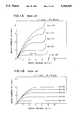
- FIG. 4Ais a graph showing the V D -I D characteristic degraded by the so-called punch through phenomenon in a conventional bulk type MOSFET.
- FIG. 4Bis a graph of the transistor characteristic where resistance is increased due to a thin silicon layer in source/drain regions in a conventional SOI-MOSFET.
- FIG. 5is a sectional view of a SOI-MOSFET according to an embodiment of the present invention.
- FIGS. 6A-6Hare sectional views of the SOI-MOSFET of the embodiment showing the manufacturing steps thereof.
- FIG. 7is a sectional view of a structure where a titanium silicide layer is formed on the surface of the source/drain regions of a bulk type MOSFET according to conventional technology associated with the present invention.
- FIG. 8is a sectional view of a CMOS having the SOI structure in which the present invention is applied to.
- FIG. 9is a graph of the V D -I D characteristic of a thin SOI-MOSFET according to the embodiments of the present invention.
- FIG. 5shows a sectional view of a thin film SOI-MOSFET of the present embodiment.
- this thin film SOI-MOSFEThas an insulator layer 12 formed on a silicon substrate 11.
- a thin silicon layer 13 of approximately 300-1500 ⁇ in thicknessis formed as a semiconductor layer on insulator layer 12.
- Silicon layer 13has a channel region 14 of low p type impurity concentration (for example 10 16 -10 17 /cm 3 ) formed in the proximity of the center thereof.
- An additional source region 15 and an additional drain region 16 each having a n type impurity concentration of an intermediate level(for example 10 18 /cm 3 ) are formed adjacent to the left and right sides of channel region 14.
- Additional source region 15 and additional drain region 16have a source region 17 and a drain region 18, respectively, of high n type impurity concentration (for example 10 19 -10 21 /cm 3 ) formed adjacent to the sides of channel region 14.
- a gate electrode 20is formed above channel region 14 with a dielectric thin film therebetween.
- the above structureis similar to the aforementioned conventional embodiment of FIG. 2.
- the present embodimentshows a first sidewall spacer 25 of relatively thin thickness where the maximum width is approximately 1000 ⁇ at the sidewall of gate electrode 20.
- a second sidewall spacer 26 having a maximum thickness of approximately 3000 ⁇is formed at the outer surface of first sidewall spacer 25.
- An additional source region 15 or an additional drain region 16is provided in silicon layer 13 beneath first sidewall spacer 25.
- a depression or reduction in film thickness due to over-etchingis not seen in second sidewall spacer 26 and in silicon layer 13 at the bottom of contact hole 23.
- metal layer 27 of low resistanceis provided on silicon layer 13 in the structure, it is possible to reduce resistance of source region 17 and drain region 18.
- oxygen ionsare implanted into silicon substrate 11 at an injection energy of 200 KeV and a dosage of 2 ⁇ 10 18 /cm 2 , followed by a heating process of approximately 1350° C.
- Thisforms an insulator layer 12 in silicon substrate 11, leaving a thin silicon layer 13 on the surface thereof.
- silicon layer 13is processed in an island-like manner to form an active region (FIG. 6A).
- a channel region 14is formed introducing impurities of p type into silicon layer 13.
- the surface of silicon layer 13is thermal-oxidized to form a dielectric thin film 19.
- a gate electrode 20 of polycrystalline siliconis formed (FIG. 6B).
- n type impuritiessuch as phosphorus ions are implanted at an injection energy of 80 KeV and a dosage of 1 ⁇ 10 13 /cm 2 to form an additional source region 15 and an additional drain region 16 of a concentration of approximately 10 18 /cm 3 (FIG. 6C).
- a CVD oxide film 25ais formed (FIG. 6D), followed by formation of a first sidewall spacer 25 by reactive ion etching (FIG. 6E).
- the film thickness of CVD oxide film 25ais approximately set to 1000 ⁇ for example, reduction in thickness of silicon layer 13 due to over-etching is very low. This is because the over-etching amount of CVD oxide film 25a is set to be approximately 200 ⁇ which is 20% of 1000 ⁇ and the etching selectivity of silicon is approximately 1/5 of CVD oxide film 25a, so that the over-etching amount of silicon layer 13 is approximately 40 ⁇ .
- a metal layer 27 of titanium silicideis formed on silicon layer 13 or on gate electrode 20 by a self-aligning method described hereinafter (FIG. 6F).
- titanium silicide layer for metal layer 27titanium is deposited all over the surface to a thickness in a range from several hundreds to a thousand ⁇ (several 100s ⁇ -1000 ⁇ ), followed by heat process to silicide the exposing portion of silicon or polycrystalline silicon, resulting in formation of a titanium silicide layer. Titanium on insulator layer 12 or on the surface of sidewall spacer 25 is left unreacted, or is nitrided to be changed to titanium nitride.
- metal layer 27 of titanium silicide layeris selectively formed on silicon layer 13 or gate electrode 20.
- a CVD oxide film of approximately 3000 ⁇ thicknessis deposited all over the surface to be subjected to anisotropic etching for forming a second sidewall spacer 26.
- n type impuritiessuch as phosphorus ions and arsenic ions are doped to form a source region 17 and a drain region 18 (FIG. 6G).
- FOG. 6Gdrain region 18
- over-etching of silicon layer 13is prevented since metal layer 27 covers silicon layer 13. This is because the etching selectivity of metal layer 27 with respect to the CVD insulating film forming sidewall spacer 26 is decreased to approximately 1/20.
- interconnection layer 24results in the sectional view of FIG. 6H.
- Interconnection layer 24is electrically connected to source region 17 and drain region 18 via metal layer 27 in contact hole 23.
- titanium silicideis described as the material of metal layer 27 in the present embodiment, similar effects can be obtained using other materials such as cobalt silicide or selective tungsten layer as long as the metal layer has conductivity and etching resistance, and is capable of being formed in self-aligmnent.
- Selective tungsten layertakes advantage of the fact that the core of tungsten is easily generated on silicon by the following reaction equation.
- a monocrystalline silicon layeris used as the semiconductor layer in the present embodiment, similar effects can be obtained using a semiconductor layer of polycrystalline silicon or gallium arsenic.
- the present inventionis applied to a thin film SOI-MOSFET in the present embodiment, the prevention of over-etching which is the object of the present invention is also effectively applicable to the so-called bulk MOSFET provided on a semiconductor substrate.
- the present inventionhas particular effect in a semiconductor device having a relatively shallow source/drain junction.
- a structure where a titanium silicide film is formed on the surface of the source/drain regions of a bulk type MOSFET of FIG. 7is disclosed in Japanese Patent Laying-Open No. 61-270870.
- the structure disclosed in the aforementioned publicationhas a gate electrode 103 formed above silicon substrate 101 with an insulating film 102 therebetween.
- sidewall spacers 105a and 105b of an insulating filmare formed which insulates gate electrode 103 from impurity diffusion layers 104a and 104b which become the source/drain regions.
- a titanium silicide film 106ais formed on impurity diffusion layer 104a.
- a titanium silicide film 106cis formed on gate electrode 103.
- a titanium silicide film 106bis formed on impurity diffusion layer 104b.
- An oxide titanium film 107ais formed on titanium silicide film 106a, sidewall spacer 105a, and titanium silicide film 106c.
- An oxide titanium film 107cis formed on titanium silicide film 106b, sidewall spacer 105b, and titanium silicide film 106c.
- An oxide titanium film 107bis formed on titanium silicide film 106b and on a relatively thick insulating film 108. According to this structure, titanium silicide layers 106a and 106b contribute to reduction in sheet resistance of impurity diffusion layers 104a and 104b.
- impurity diffusion layers 104a and 104bwill be over-etched by the anisotropic etching step in forming sidewall spacers 105a and 105b because sidewall spacers 105a and 105b of FIG. 7 are of a single layer structure relatively great in thickness.
- the application of such a structure in a semiconductor device having an active region of a thin semiconductor layer, such as a thin type SOI-MOSFET,cannot have the problem solved of increase in resistance of the source/drain regions due to over-etching.
- FIG. 8shows a sectional view of an SOI type CMOS where the present invention is applied to the conventional structure of FIG. 1A.
- silicon layers 113a and 113b as the semiconductor layerare formed in an island-like manner on a silicon substrate 111 with an insulator layer 112 therebetween.
- An n channel MOS 101is formed at silicon layer 113a.
- a p channel MOS 102is formed at silicon layer 113b.
- a p channel region 114ais formed in the middle of silicon layer 113a.
- An n type additional source region 115a and an additional drain region 116aare formed adjacent to the left and right sides of channel region 114a.
- a source region 117a and a drain region 118aare formed adjacent to additional source region 115a and additional drain region 116a, respectively.
- a gate electrode 120is formed above channel region 114a with a dielectric thin film 119 therebetween.
- a first sidewall spacer 125 and a second sidewall spacer 126 forming a double layered structureare formed at the left and right sides of gate electrode 120.
- a metal layer 127 such as of titanium silicide layeris formed on the surface of silicon layer 113a at the region outside first sidewall spacer 125 and on the surface of gate electrode 120.
- Silicon layer 113b isolated from silicon layer 113a by a field insulating film 103has a channel region 114b of the n type formed in the middle thereof.
- An additional source region 115b and an additional drain region 116b of the p typeare formed adjacent to the left and right sides of channel region 114b.
- a high concentration p type source region 117b and a drain region 118bare formed on the further outer left and right sides of additional source and drain regions of 115b and 116b, respectively.
- the structures of gate electrode 120 and first sidewall spacer 125, and second sidewall spacer 126 and metal layer 127are similar to those of the above described n channel MOS 101.
- Each channel regionhas an impurity concentration of 10 16 -10 17 /cm 3
- each additional source/drain regionhas an impurity concentration of approximately 10 18 /cm 3
- each source/drain regionhas an impurity concentration of 10 19 -10 21 /cm 3 .
- CMOScomplementary metal-oxide-semiconductor
- V D -I D characteristic of the SOI-MOSFET obtained by the above described embodimentis superior as shown in the graph of FIG. 9.
Landscapes
- Engineering & Computer Science (AREA)
- Physics & Mathematics (AREA)
- Condensed Matter Physics & Semiconductors (AREA)
- General Physics & Mathematics (AREA)
- Manufacturing & Machinery (AREA)
- Computer Hardware Design (AREA)
- Microelectronics & Electronic Packaging (AREA)
- Power Engineering (AREA)
- Thin Film Transistor (AREA)
- Metal-Oxide And Bipolar Metal-Oxide Semiconductor Integrated Circuits (AREA)
Abstract
Description
1. Field of the Invention
The present invention relates to semiconductor devices, and more particularly, to a semiconductor device having a relatively thin active region such as a MOS (Metal Oxide Semiconductor) type field effect transistor (referred to as SOI-MOSFET hereinafter) and a method of manufacturing thereof.
2. Description of the Background Art
An SOI-MOSFET to which the present invention is mainly applied will be explained first taking a complementary type MOS (referred to as CMOS hereinafter) as an example of the background technology of the present invention.
A CMOS having low consumption power and superior noise immunity is important in seeking high integration density and high speed operation. A sectional view of a conventional CMOS of not the SOI type but the so-called bulk type is shown in FIG. 1A. Referring to FIG. 1A, a CMOS has an nwell region 2 formed in the proximity of the surface of a ptype silicon substrate 1. A pchannel type MOSFET 4 comprising apolycrystalline silicon gate 4 as the main element is formed on nwell region 2. An nchannel type MOSFET 6 comprising apolycrystalline silicon gate 5 as the main element is formed at the surface of ptype silicon substrate 1 in the region other than nwell region 2. Afield oxide film 7 insulates and isolates nwell region 2 from the other region. When such a bulk type CMOS is reduced in element size, parasitic thyristor is activated by noise from outside so that abnormal current flows from the power supply terminal to the ground terminal to stop the circuit operation (latch up phenomenon). This also induces problems such as soft error by αparticle.
A sectional view of a CMOS having an SOI type structure is schematically shown in FIG. 1B. Referring to FIG. 1B, this SOI type CMOS hassemiconductor layers field insulating film 7 on asilicon substrate 1 with an insulator layer 8 therebetween.Semiconductor layer 9 has an n type channel region and p type source/drain regions ofp channel MOSFET 4 formed includingpolycrystalline silicon gate 3.Semiconductor layer 10 has a p type channel region and n type source/drain regions ofn channel MOSFET 6 formed. Such a CMOS of the SOI structure has each element and also the substrate insulation-separated so that there is no current path leading to soft error and latch up. This is advantageous to reduction of element size. It is also advantageous to high speed operation since interconnection capacitance and junction capacitance are reduced by the lower insulating layer (refer to Ouyou Butsuri (Applied Physics) Vol. 54, No. 12 (1985) pp. 1274-1283, "SOI Technology").
A structure of a conventional SOI-MOSFET and a method of manufacturing thereof will be explained hereinafter with reference to FIGS. 2, and 3A-3F. Referring to FIG. 2, a conventional SOI-MOSFET has aninsulator layer 12 formed on asilicon substrate 11. A relativelythin silicon layer 13 of approximately 300-1500Å is formed oninsulator layer 12. Near the center ofsilicon layer 13, achannel region 14 having a low p type impurity concentration (for example, 1016 -1017 /cm3) is formed. Anadditional source region 15 and anadditional drain region 16 having an n type impurity concentration of the middle degree (for example, 1018 /cm3) are formed adjacent to the sides ofchannel region 14.
Agate electrode 20 is formed abovechannel region 14 with a dielectricthin film 19 therebetween. Asidewall spacer 21 is formed at the sidewalls ofgate electrode 20.Silicon layer 13,gate electrode 20 andsidewall spacer 21 are covered with aninterlayer insulating film 22. Acontact hole 23 is provided in interlayerinsulating film 2. Aninterconnection layer 24 is connected togate electrode 20,source region 17 anddrain region 18 through eachcontact hole 23.
When positive voltage is applied togate electrode 20 in the SOI-MOSFET of the above structure, carriers (electrons) of the n conductivity type are induced towards the upper layer of ptype channel region 14, whereby that upper layer is inverted to an n conductivity type identical to the conductivity ofsource region 17 anddrain region 18, oradditional source region 15 andadditional drain region 16. This allows current to flow betweensource region 17 anddrain region 18. Because the concentration of the n type carriers induced at the upper layer ofchannel region 14 varies depending on the gate voltage, the current amount flowing acrosschannel region 14 can be controlled by the gate voltage. This explains the operation of a MOSFET.
A method of manufacturing a conventional SOI-MOSFET having the structure of FIG. 2 will be explained hereinafter with reference to FIGS. 3A-3F. First, oxygen ions are implanted into asilicon substrate 11 at an injection energy of 200 KeV and a dosage of 2×10¹⁸ /cm3. Then, the substrate is subjected to heat treatment of approximately 1350° C. An insulatinglayer 12 is formed insilicon substrate 11 leaving athin silicon layer 13 on the surface. Next,silicon layer 13 is processed in an island-like manner to form an active region (FIG. 3A). Impurities of p type are injected intosilicon layer 13 to form achannel region 14. Next, a dielectricthin film 19 is formed by thermal oxidation of the surface ofsilicon layer 13. Then, agate electrode 20 such as of polycrystalline silicon is formed. Ion implantation is carried out usinggate electrode 20 as a mask. By implanting phosphorus which is an impurity of n type for example,additional source region 15 andadditional drain region 16 are formed (FIG. 3B).
By depositing aCVD insulating film 21a (FIG. 3C) and then carrying out reactive ion etching, asidewall spacer 21 is formed at the sidewall ofgate electrode 20. Some over-etching is necessary in providingsidewall spacer 21. This is to take into consideration unevenness in the thickness ofCVD oxide film 21a which is deposited to approximately 3000Å to leave onlysidewall spacer 21 while removing the remainder by etching. This over-etching is responsible for some removal ofsilicon layer 13 to generate a step as shown in FIG. 3D by arrow A. Specifically, when the application of reactive ion etching toCVD oxide film 21a of, for example, approximately 3000Å in average is carried out with over-etching of approximately 20% on account of variation in thickness and etching characteristic ofCVD oxide film 21a. That is to say, 3000Å ofCVD oxide film 21a is first etched, followed by etching of a time period where 600Å ofCVD oxide film 21a is over-etched.Silicon layer 13 will be over-etched if the thickness of the CVD insulating film deposited thereabove is exactly 3000Å. A silicon oxide film is generally used for a CVD insulating film, where the selectivity of reactive ion etching to silicon is approximately 5: 1. This means that silicon of approximately 120Å is etched during the time period where over-etching of 600Å is carried out for a silicon oxide film.
Following the formation ofsidewall spacer 21, arsenic ions of 1019 -1020 /cm3 are injected usingsidewall spacer 21 as a mask to formsource region 17 and drainregion 18 of high concentration, as shown in FIG. 3D. Then, aninterlayer insulating film 22 is deposited by CVD, followed by formation of acontact hole 23 in a predetermined position in interlayer insulatinglayer 22. Some over-etching occurs in formingcontact hole 23 to result in a depression indicated by arrow B in FIG. 3E. The formation of aninterconnection layer 24 completes the manufacture of a thin film SOI-MOSFET of FIG. 3F.
Because a conventional SOI-MOSFET is manufactured having a structure as described above, over-etching occurs in formingsidewall spacer 21 andcontact hole 23, resulting in asilicon layer 13 having a thin portion as shown in arrow A of FIG. 3D and arrow B of FIG. 3E. The resistance of this portion is increased to deteriorate the transistor characteristic. The value of drain current ID with respect to a predetermined drain voltage VD is decreased as shown in FIG. 4B. There was also a problem that the transistor does not operate due to the fact that there is some portion wheresilicon layer 13 is completely removed to cut offsource region 17 or drainregion 18.
An object of the present invention is to provide a semiconductor device improved in transistor characteristic by suppressing decrease of film thickness in the semiconductor layer caused by over-etching, and a method of forming thereof.
A semiconductor device according to the present invention includes a semiconductor layer formed on an insulator layer, a channel region of a first conductivity type formed within the semiconductor layer, additional source/drain regions of a second conductivity type formed within the semiconductor layer adjacent to the sides of the channel region, and a gate electrode formed above the channel region with a dielectric thin film therebetween. A first sidewall spacer is formed at the sidewall of the gate electrode. An etching-resistant metal layer is formed on the surface of the semiconductor layer outside the first sidewall spacer. A second sidewall spacer is formed at the outer surface of the first sidewall spacer. Source/drain regions of a second conductivity type having a concentration higher than that of the additional source/drain regions are formed in the semiconductor layer outside the region of the second sidewall spacer adjacent to the additional source/drain regions.
A method of manufacturing a semiconductor device according to the present invention comprises the steps of forming a dielectric thin film on a semiconductor layer formed on an insulating layer, and forming a gate electrode on this dielectric thin film. Using the gate electrode as a mask, impurities of a second conductivity type are implanted into the semiconductor layer to form additional source/drain regions. A first sidewall spacer is formed at the left and right sidewalls of the gate electrode, followed by forming an etching-resistant metal layer in self-alignment at the region where the semiconductor layer is exposed excluding the surface of the first sidewall spacer. After the formation of the metal layer, a second sidewall spacer is formed at the outer surface of the first sidewall spacer. Using this second sidewall spacer as a mask, impurities of a second conductivity type are implanted to form source/drain regions having a concentration higher than that of the additional source/drain regions.
A semiconductor device and a method of manufacturing the same according to the present invention has a double layered structure of a first sidewall spacer formed at the sidewall of a gate electrode and a second sidewall spacer formed at the outer surface thereof. The first sidewall spacer is used as a mask for forming a metal layer on the surface of source/drain regions. The second sidewall spacer is used as a mask in the formation of source/drain regions of high concentration in an LDD structure. This allows the formation of the first sidewall spacer with relatively thin thickness in which the maximum width is approximately 1000Å. Therefore, over-etching of the source/drain regions is suppressed to a very low degree in anisotropic etching of forming the first sidewall spacer. The formation of an etching-resistant metal layer on the source/drain regions prevents over-etching of the source/drain regions in anisotropic etching in forming the second sidewall spacer.
The foregoing and other objects, features, aspects and advantages of the present invention will become more apparent from the following detailed description of the present invention when taken in conjunction with the accompanying drawings.
FIG. 1A is a sectional view of a conventional bulk type CMOS.
FIG. 1B is a sectional view of a conventional SOI-CMOS.
FIG. 2 is a sectional view of a conventional thin SOI-MOSFET.
FIGS. 3A-3F are sectional views of a conventional SOI-MOSFET showing the manufacturing steps thereof.
FIG. 4A is a graph showing the VD -ID characteristic degraded by the so-called punch through phenomenon in a conventional bulk type MOSFET.
FIG. 4B is a graph of the transistor characteristic where resistance is increased due to a thin silicon layer in source/drain regions in a conventional SOI-MOSFET.
FIG. 5 is a sectional view of a SOI-MOSFET according to an embodiment of the present invention.
FIGS. 6A-6H are sectional views of the SOI-MOSFET of the embodiment showing the manufacturing steps thereof.
FIG. 7 is a sectional view of a structure where a titanium silicide layer is formed on the surface of the source/drain regions of a bulk type MOSFET according to conventional technology associated with the present invention.
FIG. 8 is a sectional view of a CMOS having the SOI structure in which the present invention is applied to.
FIG. 9 is a graph of the VD -ID characteristic of a thin SOI-MOSFET according to the embodiments of the present invention.
An embodiment of the present invention will be explained hereinafter with reference to the drawings. FIG. 5 shows a sectional view of a thin film SOI-MOSFET of the present embodiment. Referring to FIG. 5, this thin film SOI-MOSFET has aninsulator layer 12 formed on asilicon substrate 11. Athin silicon layer 13 of approximately 300-1500Å in thickness is formed as a semiconductor layer oninsulator layer 12.Silicon layer 13 has achannel region 14 of low p type impurity concentration (for example 1016 -1017 /cm3) formed in the proximity of the center thereof. Anadditional source region 15 and anadditional drain region 16 each having a n type impurity concentration of an intermediate level (for example 1018 /cm3) are formed adjacent to the left and right sides ofchannel region 14.Additional source region 15 andadditional drain region 16 have asource region 17 and adrain region 18, respectively, of high n type impurity concentration (for example 1019 -1021 /cm3) formed adjacent to the sides ofchannel region 14. Agate electrode 20 is formed abovechannel region 14 with a dielectric thin film therebetween.
The above structure is similar to the aforementioned conventional embodiment of FIG. 2. The present embodiment shows afirst sidewall spacer 25 of relatively thin thickness where the maximum width is approximately 1000Å at the sidewall ofgate electrode 20. Ametal layer 27 formed of a thin titanium silicide layer of approximately 500Å in thickness, for example, is formed on the surface ofsilicon layer 13 which is not covered withgate electrode 20 orfirst sidewall spacer 25, and ongate electrode 20. Asecond sidewall spacer 26 having a maximum thickness of approximately 3000Å is formed at the outer surface offirst sidewall spacer 25. Anadditional source region 15 or anadditional drain region 16 is provided insilicon layer 13 beneathfirst sidewall spacer 25. A depression or reduction in film thickness due to over-etching is not seen insecond sidewall spacer 26 and insilicon layer 13 at the bottom ofcontact hole 23.
Becausemetal layer 27 of low resistance is provided onsilicon layer 13 in the structure, it is possible to reduce resistance ofsource region 17 and drainregion 18.
The manufacturing steps of the SOI-MOSFET of the embodiment in FIG. 5 will be explained with reference to FIGS. 6A-6H. According to the method of manufacturing an SOI-MOSFET of the present embodiment, oxygen ions are implanted intosilicon substrate 11 at an injection energy of 200 KeV and a dosage of 2×10¹⁸ /cm2, followed by a heating process of approximately 1350° C. This forms aninsulator layer 12 insilicon substrate 11, leaving athin silicon layer 13 on the surface thereof. Then,silicon layer 13 is processed in an island-like manner to form an active region (FIG. 6A). Achannel region 14 is formed introducing impurities of p type intosilicon layer 13. The surface ofsilicon layer 13 is thermal-oxidized to form a dielectricthin film 19. Then, agate electrode 20 of polycrystalline silicon is formed (FIG. 6B). Usinggate electrode 20 as a mask, n type impurities such as phosphorus ions are implanted at an injection energy of 80 KeV and a dosage of 1×10¹³ /cm2 to form anadditional source region 15 and anadditional drain region 16 of a concentration of approximately 1018 /cm3 (FIG. 6C).
The above described manufacturing steps are similar to those of the aforementioned conventional embodiment. In the present embodiment, aCVD oxide film 25a is formed (FIG. 6D), followed by formation of afirst sidewall spacer 25 by reactive ion etching (FIG. 6E). If the film thickness ofCVD oxide film 25a is approximately set to 1000Å for example, reduction in thickness ofsilicon layer 13 due to over-etching is very low. This is because the over-etching amount ofCVD oxide film 25a is set to be approximately 200Å which is 20% of 1000Å and the etching selectivity of silicon is approximately 1/5 ofCVD oxide film 25a, so that the over-etching amount ofsilicon layer 13 is approximately 40Å.
Ametal layer 27 of titanium silicide, for example, is formed onsilicon layer 13 or ongate electrode 20 by a self-aligning method described hereinafter (FIG. 6F). In forming a titanium silicide layer formetal layer 27, titanium is deposited all over the surface to a thickness in a range from several hundreds to a thousand Å (several 100sÅ-1000Å), followed by heat process to silicide the exposing portion of silicon or polycrystalline silicon, resulting in formation of a titanium silicide layer. Titanium oninsulator layer 12 or on the surface ofsidewall spacer 25 is left unreacted, or is nitrided to be changed to titanium nitride. By removing the unreacted titanium or titanium nitride with sulfuric acid,metal layer 27 of titanium silicide layer is selectively formed onsilicon layer 13 orgate electrode 20. Next, a CVD oxide film of approximately 3000Å thickness is deposited all over the surface to be subjected to anisotropic etching for forming asecond sidewall spacer 26. Usingsidewall spacer 26 as a mask, n type impurities such as phosphorus ions and arsenic ions are doped to form asource region 17 and a drain region 18 (FIG. 6G). In formingsecond sidewall spacer 26, over-etching ofsilicon layer 13 is prevented sincemetal layer 27covers silicon layer 13. This is because the etching selectivity ofmetal layer 27 with respect to the CVD insulating film formingsidewall spacer 26 is decreased to approximately 1/20.
The formation ofinterconnection layer 24 results in the sectional view of FIG. 6H.Interconnection layer 24 is electrically connected to sourceregion 17 and drainregion 18 viametal layer 27 incontact hole 23.
Although titanium silicide is described as the material ofmetal layer 27 in the present embodiment, similar effects can be obtained using other materials such as cobalt silicide or selective tungsten layer as long as the metal layer has conductivity and etching resistance, and is capable of being formed in self-aligmnent. Selective tungsten layer takes advantage of the fact that the core of tungsten is easily generated on silicon by the following reaction equation.
WF.sub.6 +Si→W+SiF.sub.6 ↑
Although a monocrystalline silicon layer is used as the semiconductor layer in the present embodiment, similar effects can be obtained using a semiconductor layer of polycrystalline silicon or gallium arsenic.
Although the present embodiment is described in which an n channel MOSFET is employed, a p channel MOSFET may be used. Identical effects can be obtained with only the conductivity type reversed.
Although the present invention is applied to a thin film SOI-MOSFET in the present embodiment, the prevention of over-etching which is the object of the present invention is also effectively applicable to the so-called bulk MOSFET provided on a semiconductor substrate. The present invention has particular effect in a semiconductor device having a relatively shallow source/drain junction.
As a conventional technology associated with the above described embodiment, a structure where a titanium silicide film is formed on the surface of the source/drain regions of a bulk type MOSFET of FIG. 7 is disclosed in Japanese Patent Laying-Open No. 61-270870. Referring to FIG. 7, the structure disclosed in the aforementioned publication has agate electrode 103 formed abovesilicon substrate 101 with an insulatingfilm 102 therebetween. At the left and right sides ofgate electrode 103, sidewall spacers 105a and 105b of an insulating film are formed which insulatesgate electrode 103 fromimpurity diffusion layers titanium silicide film 106a is formed onimpurity diffusion layer 104a. Atitanium silicide film 106c is formed ongate electrode 103. Atitanium silicide film 106b is formed onimpurity diffusion layer 104b. Anoxide titanium film 107a is formed ontitanium silicide film 106a, sidewall spacer 105a, andtitanium silicide film 106c. Anoxide titanium film 107c is formed ontitanium silicide film 106b,sidewall spacer 105b, andtitanium silicide film 106c. An oxide titanium film 107b is formed ontitanium silicide film 106b and on a relatively thickinsulating film 108. According to this structure,titanium silicide layers impurity diffusion layers
However,impurity diffusion layers sidewall spacers
An embodiment where the present invention is applied to a CMOS having an SOI structure will be explained hereinafter. FIG. 8 shows a sectional view of an SOI type CMOS where the present invention is applied to the conventional structure of FIG. 1A. Referring to FIG. 8,silicon layers 113a and 113b as the semiconductor layer are formed in an island-like manner on asilicon substrate 111 with aninsulator layer 112 therebetween. Ann channel MOS 101 is formed at silicon layer 113a. Ap channel MOS 102 is formed atsilicon layer 113b. Specifically,a p channel region 114a is formed in the middle of silicon layer 113a. An n typeadditional source region 115a and anadditional drain region 116a are formed adjacent to the left and right sides ofchannel region 114a. Asource region 117a and adrain region 118a are formed adjacent toadditional source region 115a andadditional drain region 116a, respectively. Agate electrode 120 is formed abovechannel region 114a with a dielectricthin film 119 therebetween. Afirst sidewall spacer 125 and asecond sidewall spacer 126 forming a double layered structure are formed at the left and right sides ofgate electrode 120. Ametal layer 127 such as of titanium silicide layer is formed on the surface of silicon layer 113a at the region outsidefirst sidewall spacer 125 and on the surface ofgate electrode 120.Silicon layer 113b isolated from silicon layer 113a by afield insulating film 103 has achannel region 114b of the n type formed in the middle thereof. Anadditional source region 115b and anadditional drain region 116b of the p type are formed adjacent to the left and right sides ofchannel region 114b. A high concentration ptype source region 117b and adrain region 118b are formed on the further outer left and right sides of additional source and drain regions of 115b and 116b, respectively. The structures ofgate electrode 120 andfirst sidewall spacer 125, andsecond sidewall spacer 126 andmetal layer 127 are similar to those of the above describedn channel MOS 101. Each channel region has an impurity concentration of 1016 -1017 /cm3, each additional source/drain region has an impurity concentration of approximately 1018 /cm3, and each source/drain region has an impurity concentration of 1019 -1021 /cm3.
According to an SOI type CMOS having the above described structure is free of soft error and latch up phenomenon. Also, resistance of the source/drain regions are held low to improve the current characteristic of the transistor.
The VD -ID characteristic of the SOI-MOSFET obtained by the above described embodiment is superior as shown in the graph of FIG. 9.
Although the present invention has been described and illustrated in detail, it is clearly understood that the same is by way of illustration and example only and is not to be taken by way of limitation, the spirit and scope of the present invention being limited only by the terms of the appended claims.
Claims (2)
1. A semiconductor device comprising:
a semiconductor layer formed on an insulator layer,
a channel region of a first conductivity type formed in said semiconductor layer,
first source/drain regions of a second conductivity type formed in said semiconductor layer adjacent to the left and right sides of said channel region,
a gate electrode formed above said channel region with a dielectric thin film therebetween, first sidewall spacers provided on the left and right sidewalls of said gate electrode,
a metal layer having etching-resistance formed at the surface of said semiconductor layer in a region outside the region where said first sidewall spacers are formed and adjacent to said first sidewall spacers,
second sidewall spacers provided to cover the outer surface of said first sidewall spacers,
second source/drain regions having a concentration higher than that of said first source/drain regions, and formed in said semiconductor layer in a region outside the region where said second sidewall spacers are formed, and
an interconnection layer connected to a surface of said metal layer, wherein said metal layer comprises a titanium silicide layer of approximately 500Å in thickness.
2. A semiconductor device comprising:
two semiconductor layers formed on a same insulator layer insulation-isolated from each other;
a gate electrode formed above each of said semiconductor layers with a gate dielectric thin film therebetween;
first sidewall spacers provided at the left and right sidewalls of each said gate electrode;
a metal layer having etching-resistance, and formed in a region outside the region where said first sidewall spacers are formed at the surface of each said semiconductor layer and adjacent to said first sidewall spacers;
second sidewall spacers formed to cover the outer surface of each of said first sidewall spacers; and
an interconnection layer connected to a surface of said metal layer; wherein
one of said two semiconductor layers comprises
a channel region of p type right beneath said gate electrode;
first source/drain regions of n type formed adjacent to the left and right sides of said channel region; and
second source/drain regions of n type having a concentration higher than that of said first source-drain regions of n type, and formed adjacent to said first source/drain regions of n type at a region outside the region where said second sidewall spacers are formed, and the other semiconductor layer comprises
a channel region of n type right beneath said gate electrode;
first source/drain regions of p type formed adjacent to the left and right sides of said channel region; and
second source/drain regions of p type having a concentration higher than that of said first source-drain regions of p type, and formed adjacent to said first source/drain regions of p type in a region outside the region where said second sidewall spacers are formed, wherein said metal layer comprises a titanium silicide layer of approximately 500Å in thickness.
Priority Applications (1)
| Application Number | Priority Date | Filing Date | Title |
|---|---|---|---|
| US08/268,877US5444282A (en) | 1990-10-09 | 1994-06-30 | Semiconductor device and a method of manufacturing thereof |
Applications Claiming Priority (2)
| Application Number | Priority Date | Filing Date | Title |
|---|---|---|---|
| JP2271727AJP2940880B2 (en) | 1990-10-09 | 1990-10-09 | Semiconductor device and manufacturing method thereof |
| JP2-271727 | 1990-10-09 |
Related Child Applications (1)
| Application Number | Title | Priority Date | Filing Date |
|---|---|---|---|
| US08/268,877ContinuationUS5444282A (en) | 1990-10-09 | 1994-06-30 | Semiconductor device and a method of manufacturing thereof |
Publications (1)
| Publication Number | Publication Date |
|---|---|
| US5341028Atrue US5341028A (en) | 1994-08-23 |
Family
ID=17504002
Family Applications (2)
| Application Number | Title | Priority Date | Filing Date |
|---|---|---|---|
| US07/770,041Expired - LifetimeUS5341028A (en) | 1990-10-09 | 1991-10-03 | Semiconductor device and a method of manufacturing thereof |
| US08/268,877Expired - Fee RelatedUS5444282A (en) | 1990-10-09 | 1994-06-30 | Semiconductor device and a method of manufacturing thereof |
Family Applications After (1)
| Application Number | Title | Priority Date | Filing Date |
|---|---|---|---|
| US08/268,877Expired - Fee RelatedUS5444282A (en) | 1990-10-09 | 1994-06-30 | Semiconductor device and a method of manufacturing thereof |
Country Status (4)
| Country | Link |
|---|---|
| US (2) | US5341028A (en) |
| EP (1) | EP0480635B1 (en) |
| JP (1) | JP2940880B2 (en) |
| DE (1) | DE69111963T2 (en) |
Cited By (51)
| Publication number | Priority date | Publication date | Assignee | Title |
|---|---|---|---|---|
| US5444282A (en)* | 1990-10-09 | 1995-08-22 | Mitsubishi Denki Kabushiki Kaisha | Semiconductor device and a method of manufacturing thereof |
| US5514880A (en)* | 1992-10-28 | 1996-05-07 | Mitsubishi Denki Kabushiki Kaisha | Field effect thin-film transistor for an SRAM with reduced standby current |
| US5656845A (en)* | 1995-03-08 | 1997-08-12 | Atmel Corporation | EEPROM on insulator |
| US5659194A (en)* | 1994-01-28 | 1997-08-19 | Mitsubishi Denki Kabushiki Kaisha | Semiconductor device having metal silicide film |
| US5705839A (en)* | 1995-11-13 | 1998-01-06 | Taiwan Semiconductor Manufacturing Company, Ltd. | Gate spacer to control the base width of a lateral bipolar junction transistor using SOI technology |
| US5763923A (en)* | 1996-08-13 | 1998-06-09 | Micron Technology, Inc. | Compound PVD target material for semiconductor metallization |
| US5783842A (en)* | 1993-01-18 | 1998-07-21 | Canon Kabushiki Kaisha | Semiconductor device having an insulating layer having a concave section formed by oxidizing a semiconductor layer |
| US5804858A (en)* | 1995-06-08 | 1998-09-08 | Taiwan Semiconductor Manufacturing, Ltd. | Body contacted SOI MOSFET |
| US5841173A (en)* | 1995-06-16 | 1998-11-24 | Matsushita Electric Industrial Co., Ltd. | MOS semiconductor device with excellent drain current |
| US5962897A (en)* | 1992-06-18 | 1999-10-05 | Semiconductor Energy Laboratory Co., Ltd. | Semiconductor device and method for forming the same |
| US6037233A (en)* | 1998-04-27 | 2000-03-14 | Lsi Logic Corporation | Metal-encapsulated polysilicon gate and interconnect |
| US6049092A (en)* | 1993-09-20 | 2000-04-11 | Semiconductor Energy Laboratory Co., Ltd. | Semiconductor device and method for manufacturing the same |
| US6071825A (en)* | 1995-07-19 | 2000-06-06 | Interuniversitaire Microelektronica Centrum (Imec Vzw) | Fully overlapped nitride-etch defined device and processing sequence |
| US6075268A (en)* | 1996-11-07 | 2000-06-13 | Advanced Micro Devices, Inc. | Ultra high density inverter using a stacked transistor arrangement |
| US6172381B1 (en) | 1997-06-20 | 2001-01-09 | Advanced Micro Devices, Inc. | Source/drain junction areas self aligned between a sidewall spacer and an etched lateral sidewall |
| US6218276B1 (en) | 1997-12-22 | 2001-04-17 | Lsi Logic Corporation | Silicide encapsulation of polysilicon gate and interconnect |
| US6218678B1 (en) | 1993-11-05 | 2001-04-17 | Semiconductor Energy Laboratory Co., Ltd. | Semiconductor device |
| US6225663B1 (en) | 1996-06-14 | 2001-05-01 | Mitsubishi Denki Kabushiki Kaisha | Semiconductor device having SOI structure and method of fabricating the same |
| US6232637B1 (en) | 1997-05-02 | 2001-05-15 | Advanced Micro Devices, Inc. | Semiconductor fabrication having multi-level transistors and high density interconnect therebetween |
| US6306676B1 (en) | 1996-04-04 | 2001-10-23 | Eastman Kodak Company | Method of making self-aligned, high-enegry implanted photodiode for solid-state image sensors |
| US6337504B1 (en)* | 1997-03-10 | 2002-01-08 | Denso Corporation | Insulated gate transistor with leakage current prevention feature |
| US6358828B1 (en) | 1997-06-20 | 2002-03-19 | Advanced Micro Devices, Inc. | Ultra high density series-connected transistors formed on separate elevational levels |
| US20020048841A1 (en)* | 1999-10-22 | 2002-04-25 | International Business Machines Corporation | Disposable spacer for symmetric and asymmetric schottky contact to SOI mosfet |
| US20020149038A1 (en)* | 2001-04-04 | 2002-10-17 | Yoshifumi Yoshida | Semiconductor device |
| US20030042547A1 (en)* | 2000-03-22 | 2003-03-06 | Simon Deleonibus | Metal source and drain mos transistor, and method for making same |
| US6624477B1 (en) | 1992-10-09 | 2003-09-23 | Semiconductor Energy Laboratory Co., Ltd. | Semiconductor device and method for manufacturing the same |
| US20030183821A1 (en)* | 1994-05-26 | 2003-10-02 | Semiconductor Energy Laboratory Co., Ltd. | Semiconductor integrated circuit and method of fabricating same |
| US6656814B2 (en)* | 1998-06-30 | 2003-12-02 | Samsung Electronics Co., Ltd. | Methods of fabricating integrated circuit devices including distributed and isolated dummy conductive regions |
| US6674127B2 (en)* | 2000-04-27 | 2004-01-06 | Matsushita Electric Industrial Co., Ltd. | Semiconductor integrated circuit |
| US20040147095A1 (en)* | 1998-06-22 | 2004-07-29 | Semiconductor Energy Laboratory Co., Ltd. | Method of manufacturing a semiconductor device |
| US20050009252A1 (en)* | 1998-09-04 | 2005-01-13 | Semiconductor Energy Laboratory Co., Ltd. | Method of fabricating a semiconductor device |
| US20050106789A1 (en)* | 2002-03-26 | 2005-05-19 | Infineon Technologies Ag | Method for producing an SOI field effect transistor and corresponding field effect transistor |
| US20050159940A1 (en)* | 1999-05-27 | 2005-07-21 | America Online, Inc., A Delaware Corporation | Method and system for reduction of quantization-induced block-discontinuities and general purpose audio codec |
| US20050230755A1 (en)* | 1996-02-23 | 2005-10-20 | Semiconductor Energy Laboratory Co., Ltd. | Semiconductor thin film and its manufacturing method and semiconductor device and it's manufacturing method |
| US20060099729A1 (en)* | 2004-11-04 | 2006-05-11 | International Business Machines Corporation | Structure and method of making a semiconductor integrated circuit tolerant of mis-alignment of a metal contact pattern |
| US20070108510A1 (en)* | 1998-07-29 | 2007-05-17 | Takeshi Fukunaga | Process for production of SOI substrate and process for production of semiconductor device |
| US20070117293A1 (en)* | 1998-08-07 | 2007-05-24 | Semiconductor Energy Laboratory Co., Ltd. | Semiconductor device and method of manufacturing the same |
| US20070126058A1 (en)* | 2005-12-02 | 2007-06-07 | Semiconductor Energy Laboratory Co., Ltd. | Semiconductor device and manufacturing method thereof |
| US20070252206A1 (en)* | 1996-02-23 | 2007-11-01 | Semiconductor Energy Laboratory Co., Ltd. | Semiconductor thin film and method of manufacturing the same and semiconductor device and method of manufacturing the same |
| US20080203501A1 (en)* | 2007-02-22 | 2008-08-28 | Semiconductor Energy Laboratory Co., Ltd. | Semiconductor device |
| US20080217688A1 (en)* | 2007-03-08 | 2008-09-11 | Semiconductor Energy Laboratory Co., Ltd. | Semiconductor device and manufacture method thereof |
| US20080230835A1 (en)* | 2007-03-23 | 2008-09-25 | Semiconductor Energy Laboratory Co., Ltd. | Semiconductor device and manufacturing method thereof |
| US20080237876A1 (en)* | 2007-03-26 | 2008-10-02 | Semiconductor Energy Laboratory Co., Ltd. | Semiconductor device and method for manufacturing the same |
| US20080237875A1 (en)* | 2007-03-26 | 2008-10-02 | Semiconductor Energy Laboratory Co., Ltd. | Semiconductor device and method for manufacturing the same |
| US20100051916A1 (en)* | 2000-10-04 | 2010-03-04 | Cambridge University Technical Services Limited | Method for forming an electronic device in multi-layer structure |
| US20100068860A1 (en)* | 1994-07-14 | 2010-03-18 | Semiconductor Energy Laboratory Co., Ltd. | Semiconductor device and method of manufacture thereof |
| US7863619B2 (en) | 1993-10-01 | 2011-01-04 | Semiconductor Energy Laboratory Co., Ltd. | Semiconductor device and a method for manufacturing the same |
| US8222696B2 (en) | 1997-11-18 | 2012-07-17 | Semiconductor Energy Laboratory Co., Ltd. | Semiconductor device having buried oxide film |
| JP2015164185A (en)* | 2014-01-30 | 2015-09-10 | 株式会社半導体エネルギー研究所 | Semiconductor device manufacturing method |
| CN105185785A (en)* | 2014-06-13 | 2015-12-23 | 瑞萨电子株式会社 | Semiconductor device and manufacturing method of the same |
| US20170243649A1 (en)* | 2016-02-19 | 2017-08-24 | Nscore, Inc. | Nonvolatile memory cell employing hot carrier effect for data storage |
Families Citing this family (38)
| Publication number | Priority date | Publication date | Assignee | Title |
|---|---|---|---|---|
| WO1995003629A1 (en) | 1993-07-26 | 1995-02-02 | Seiko Epson Corporation | Thin film semiconductor device, its manufacture, and display system |
| JPH07135324A (en)* | 1993-11-05 | 1995-05-23 | Semiconductor Energy Lab Co Ltd | Thin film semiconductor integrated circuit |
| JPH07183526A (en)* | 1993-12-22 | 1995-07-21 | Toshiba Corp | Thin film semiconductor device and manufacturing method thereof |
| JP3253808B2 (en)* | 1994-07-07 | 2002-02-04 | 株式会社半導体エネルギー研究所 | Semiconductor device and manufacturing method thereof |
| US6773971B1 (en)* | 1994-07-14 | 2004-08-10 | Semiconductor Energy Laboratory Co., Ltd. | Method of manufacturing a semiconductor device having lightly-doped drain (LDD) regions |
| US5675167A (en) | 1994-11-24 | 1997-10-07 | Nippondenso Co., Ltd. | Enhancement-type semiconductor having reduced leakage current |
| EP0772242B1 (en)* | 1995-10-30 | 2006-04-05 | STMicroelectronics S.r.l. | Single feature size MOS technology power device |
| JP3263299B2 (en)* | 1995-12-04 | 2002-03-04 | 株式会社東芝 | Semiconductor device and manufacturing method thereof |
| KR100209937B1 (en)* | 1995-12-30 | 1999-07-15 | 김영환 | Transistor manufacturing method of semiconductor device |
| JPH1022466A (en)* | 1996-03-01 | 1998-01-23 | Motorola Inc | Ferroelectric nonvolatile memory cell and method of forming memory cell |
| US5789802A (en)* | 1996-06-21 | 1998-08-04 | Advanced Micro Devices, Inc. | Dopant profile spreading for arsenic source/drain |
| US6236085B1 (en) | 1996-11-11 | 2001-05-22 | Denso Corporation | Semiconductor memory device having high-concentration region around electric-field moderating layer in substrate |
| US5869879A (en)* | 1996-12-06 | 1999-02-09 | Advanced Micro Devices, Inc. | CMOS integrated circuit having a sacrificial metal spacer for producing graded NMOS source/drain junctions dissimilar from PMOS source/drain junctions |
| US5766969A (en)* | 1996-12-06 | 1998-06-16 | Advanced Micro Devices, Inc. | Multiple spacer formation/removal technique for forming a graded junction |
| US5869866A (en) | 1996-12-06 | 1999-02-09 | Advanced Micro Devices, Inc. | Integrated circuit having sacrificial spacers for producing graded NMOS source/drain junctions possibly dissimilar from PMOS source/drain junctions |
| JPH10173177A (en)* | 1996-12-10 | 1998-06-26 | Mitsubishi Electric Corp | Method for manufacturing MIS transistor |
| KR100212693B1 (en)* | 1996-12-14 | 1999-08-02 | 권혁준 | Silicon / Silicon Germanium Morse Field Transistors and Manufacturing Method Thereof |
| US5895955A (en)* | 1997-01-10 | 1999-04-20 | Advanced Micro Devices, Inc. | MOS transistor employing a removable, dual layer etch stop to protect implant regions from sidewall spacer overetch |
| US5793089A (en)* | 1997-01-10 | 1998-08-11 | Advanced Micro Devices, Inc. | Graded MOS transistor junction formed by aligning a sequence of implants to a selectively removable polysilicon sidewall space and oxide thermally grown thereon |
| JPH1168103A (en)* | 1997-08-22 | 1999-03-09 | Mitsubishi Electric Corp | Method for manufacturing semiconductor device |
| JPH1197704A (en)* | 1997-09-20 | 1999-04-09 | Semiconductor Energy Lab Co Ltd | Semiconductor device and manufacture of the same |
| US5994736A (en)* | 1997-09-22 | 1999-11-30 | United Microelectronics Corporation | Semiconductor device having buried gate electrode with silicide layer and manufacture method thereof |
| KR100302187B1 (en)* | 1997-10-08 | 2001-11-22 | 윤종용 | Method for fabricating semiconductor device |
| US6603180B1 (en)* | 1997-11-28 | 2003-08-05 | Advanced Micro Devices, Inc. | Semiconductor device having large-area silicide layer and process of fabrication thereof |
| US5982001A (en)* | 1998-03-30 | 1999-11-09 | Texas Instruments - Acer Incorporated | MOSFETS structure with a recessed self-aligned silicide contact and an extended source/drain junction |
| US6124610A (en) | 1998-06-26 | 2000-09-26 | Advanced Micro Devices, Inc. | Isotropically etching sidewall spacers to be used for both an NMOS source/drain implant and a PMOS LDD implant |
| US6437404B1 (en)* | 2000-08-10 | 2002-08-20 | Advanced Micro Devices, Inc. | Semiconductor-on-insulator transistor with recessed source and drain |
| US7189997B2 (en) | 2001-03-27 | 2007-03-13 | Semiconductor Energy Laboratory Co., Ltd. | Semiconductor device and method for manufacturing the same |
| US6982194B2 (en)* | 2001-03-27 | 2006-01-03 | Semiconductor Energy Laboratory Co., Ltd. | Semiconductor device and method for manufacturing the same |
| US20050026342A1 (en)* | 2003-07-28 | 2005-02-03 | Ka-Hing Fung | Semiconductor device having improved short channel effects, and method of forming thereof |
| KR100683852B1 (en)* | 2004-07-02 | 2007-02-15 | 삼성전자주식회사 | Mask ROM Device of Semiconductor Device and Formation Method |
| US7348248B2 (en)* | 2005-07-12 | 2008-03-25 | Taiwan Semiconductor Manufacturing Company, Ltd. | CMOS transistor with high drive current and low sheet resistance |
| KR100677048B1 (en)* | 2005-10-04 | 2007-02-01 | 동부일렉트로닉스 주식회사 | Semiconductor device and manufacturing method thereof |
| US20070095739A1 (en)* | 2005-10-24 | 2007-05-03 | Nikon Corporation | Utility transfer apparatus, stage apparatus, exposure apparatus, and device manufacturing method |
| US7696024B2 (en)* | 2006-03-31 | 2010-04-13 | Semiconductor Energy Laboratory Co., Ltd. | Semiconductor device and manufacturing method thereof |
| US7510923B2 (en) | 2006-12-19 | 2009-03-31 | Texas Instruments Incorporated | Slim spacer implementation to improve drive current |
| JP2011216894A (en)* | 2011-05-31 | 2011-10-27 | Semiconductor Energy Lab Co Ltd | Method of manufacturing semiconductor apparatus |
| JP2018157206A (en)* | 2017-03-17 | 2018-10-04 | 株式会社リコー | FIELD EFFECT TRANSISTOR AND METHOD FOR MANUFACTURING THE SAME, DISPLAY ELEMENT, DISPLAY DEVICE, AND SYSTEM |
Citations (9)
| Publication number | Priority date | Publication date | Assignee | Title |
|---|---|---|---|---|
| JPS60186053A (en)* | 1984-03-06 | 1985-09-21 | Seiko Epson Corp | Thin film complementary mos circuit |
| JPS61137367A (en)* | 1984-12-10 | 1986-06-25 | Hitachi Ltd | Manufacture of semiconductor integrated circuit device |
| JPS61270870A (en)* | 1985-05-25 | 1986-12-01 | Mitsubishi Electric Corp | Semiconductor device |
| JPS6232653A (en)* | 1985-08-05 | 1987-02-12 | Nippon Telegr & Teleph Corp <Ntt> | Manufacturing method of thin film transistor |
| JPS62143473A (en)* | 1985-12-18 | 1987-06-26 | Hitachi Ltd | semiconductor equipment |
| JPS6312168A (en)* | 1986-07-03 | 1988-01-19 | Oki Electric Ind Co Ltd | LDDMIS field effect transistor |
| JPS6384064A (en)* | 1986-09-26 | 1988-04-14 | Seiko Epson Corp | semiconductor equipment |
| JPH02181934A (en)* | 1989-01-07 | 1990-07-16 | Mitsubishi Electric Corp | MIS type semiconductor device and its manufacturing method |
| US5040037A (en)* | 1988-12-13 | 1991-08-13 | Mitsubishi Denki Kabushiki Kaisha | MOS type field effect transistor formed on a semiconductor layer on an insulator substrate |
Family Cites Families (6)
| Publication number | Priority date | Publication date | Assignee | Title |
|---|---|---|---|---|
| JPS62296563A (en)* | 1986-06-17 | 1987-12-23 | Matsushita Electronics Corp | Insulated-gate transistor and manufacture thereof |
| JPS63292679A (en)* | 1987-05-25 | 1988-11-29 | Mitsubishi Electric Corp | Manufacturing method of MOS transistor |
| JPS6427272A (en)* | 1987-07-23 | 1989-01-30 | Agency Ind Science Techn | Semiconductor device |
| JPH01291464A (en)* | 1988-05-19 | 1989-11-24 | Fujitsu Ltd | MIS field effect semiconductor device |
| JPH077773B2 (en)* | 1989-03-01 | 1995-01-30 | 工業技術院長 | Method for manufacturing semiconductor device |
| JP2940880B2 (en)* | 1990-10-09 | 1999-08-25 | 三菱電機株式会社 | Semiconductor device and manufacturing method thereof |
- 1990
- 1990-10-09JPJP2271727Apatent/JP2940880B2/ennot_activeExpired - Lifetime
- 1991
- 1991-10-03EPEP91309095Apatent/EP0480635B1/ennot_activeExpired - Lifetime
- 1991-10-03USUS07/770,041patent/US5341028A/ennot_activeExpired - Lifetime
- 1991-10-03DEDE69111963Tpatent/DE69111963T2/ennot_activeExpired - Fee Related
- 1994
- 1994-06-30USUS08/268,877patent/US5444282A/ennot_activeExpired - Fee Related
Patent Citations (10)
| Publication number | Priority date | Publication date | Assignee | Title |
|---|---|---|---|---|
| JPS60186053A (en)* | 1984-03-06 | 1985-09-21 | Seiko Epson Corp | Thin film complementary mos circuit |
| JPS61137367A (en)* | 1984-12-10 | 1986-06-25 | Hitachi Ltd | Manufacture of semiconductor integrated circuit device |
| JPS61270870A (en)* | 1985-05-25 | 1986-12-01 | Mitsubishi Electric Corp | Semiconductor device |
| JPS6232653A (en)* | 1985-08-05 | 1987-02-12 | Nippon Telegr & Teleph Corp <Ntt> | Manufacturing method of thin film transistor |
| JPS62143473A (en)* | 1985-12-18 | 1987-06-26 | Hitachi Ltd | semiconductor equipment |
| JPS6312168A (en)* | 1986-07-03 | 1988-01-19 | Oki Electric Ind Co Ltd | LDDMIS field effect transistor |
| US4873557A (en)* | 1986-07-03 | 1989-10-10 | Oki Electric Industry Co., Ltd. | MIS FET and process of fabricating the same |
| JPS6384064A (en)* | 1986-09-26 | 1988-04-14 | Seiko Epson Corp | semiconductor equipment |
| US5040037A (en)* | 1988-12-13 | 1991-08-13 | Mitsubishi Denki Kabushiki Kaisha | MOS type field effect transistor formed on a semiconductor layer on an insulator substrate |
| JPH02181934A (en)* | 1989-01-07 | 1990-07-16 | Mitsubishi Electric Corp | MIS type semiconductor device and its manufacturing method |
Non-Patent Citations (4)
| Title |
|---|
| "SOI Technology", Ouyou Batsuri (Applied Physics), vol. 54, No. 12, Nishimura et al., 1985. |
| "SOI Technology", Ouyou Butsuri (Applied Physics), vol 54, No. 12, by Tadashi Nishimura et al, pp. 1274-1283, 1985. |
| SOI Technology , Ouyou Batsuri (Applied Physics), vol. 54, No. 12, Nishimura et al., 1985.* |
| SOI Technology , Ouyou Butsuri (Applied Physics), vol 54, No. 12, by Tadashi Nishimura et al, pp. 1274 1283, 1985.* |
Cited By (143)
| Publication number | Priority date | Publication date | Assignee | Title |
|---|---|---|---|---|
| US5444282A (en)* | 1990-10-09 | 1995-08-22 | Mitsubishi Denki Kabushiki Kaisha | Semiconductor device and a method of manufacturing thereof |
| US5962897A (en)* | 1992-06-18 | 1999-10-05 | Semiconductor Energy Laboratory Co., Ltd. | Semiconductor device and method for forming the same |
| US8017506B2 (en) | 1992-10-09 | 2011-09-13 | Semiconductor Energy Laboratory Co., Ltd. | Semiconductor device and method for forming the same |
| US20100041187A1 (en)* | 1992-10-09 | 2010-02-18 | Semiconductor Energy Laboratory Co., Ltd. | Semiconductor device and method for forming the same |
| US20090152631A1 (en)* | 1992-10-09 | 2009-06-18 | Semiconductor Energy Laboratory Co., Ltd. | Semiconductor device and method for forming the same |
| US20030006414A1 (en)* | 1992-10-09 | 2003-01-09 | Semiconductor Energy Laboratory Co., Ltd. | Semiconductor device and method for forming the same |
| US7723788B2 (en) | 1992-10-09 | 2010-05-25 | Semiconductor Energy Laboratory Co., Ltd. | Semiconductor device and method for forming the same |
| US6624477B1 (en) | 1992-10-09 | 2003-09-23 | Semiconductor Energy Laboratory Co., Ltd. | Semiconductor device and method for manufacturing the same |
| US6455875B2 (en) | 1992-10-09 | 2002-09-24 | Semiconductor Energy Laboratory Co., Ltd. | Thin film transistor having enhanced field mobility |
| US7602020B2 (en) | 1992-10-09 | 2009-10-13 | Semiconductor Energy Laboratory Co., Ltd. | Semiconductor device and method for forming the same |
| US6790749B2 (en) | 1992-10-09 | 2004-09-14 | Semiconductor Energy Laboratory Co., Ltd. | Method of manufacturing a semiconductor device |
| US7109108B2 (en) | 1992-10-09 | 2006-09-19 | Semiconductor Energy Laboratory Co., Ltd. | Method for manufacturing semiconductor device having metal silicide |
| US20050037549A1 (en)* | 1992-10-09 | 2005-02-17 | Semiconductor Energy Laboratory Co., Ltd. | Semiconductor device and method for forming the same |
| US5514880A (en)* | 1992-10-28 | 1996-05-07 | Mitsubishi Denki Kabushiki Kaisha | Field effect thin-film transistor for an SRAM with reduced standby current |
| US5736438A (en)* | 1992-10-28 | 1998-04-07 | Mitsubishi Denki Kabushiki Kaisha | Field effect thin-film transistor and method of manufacturing the same as well as semiconductor device provided with the same |
| US5783842A (en)* | 1993-01-18 | 1998-07-21 | Canon Kabushiki Kaisha | Semiconductor device having an insulating layer having a concave section formed by oxidizing a semiconductor layer |
| US7381599B2 (en) | 1993-09-20 | 2008-06-03 | Semiconductor Energy Laboratory Co., Ltd. | Semiconductor device and method for manufacturing the same |
| US20110068339A1 (en)* | 1993-09-20 | 2011-03-24 | Semiconductor Energy Laboratory Co., Ltd. | Semiconductor device and method for manufacturing the same |
| US20090289254A1 (en)* | 1993-09-20 | 2009-11-26 | Semiconductor Energy Laboratory Co., Ltd. | Semiconductor device and method for manufacturing the same |
| US6049092A (en)* | 1993-09-20 | 2000-04-11 | Semiconductor Energy Laboratory Co., Ltd. | Semiconductor device and method for manufacturing the same |
| US6867431B2 (en)* | 1993-09-20 | 2005-03-15 | Semiconductor Energy Laboratory Co., Ltd. | Semiconductor device and method for manufacturing the same |
| US7569856B2 (en) | 1993-09-20 | 2009-08-04 | Semiconductor Energy Laboratory Co., Ltd. | Semiconductor device and method for manufacturing the same |
| US7525158B2 (en) | 1993-09-20 | 2009-04-28 | Semiconductor Energy Laboratory Co., Ltd. | Semiconductor device having pixel electrode and peripheral circuit |
| US20050142705A1 (en)* | 1993-09-20 | 2005-06-30 | Semiconductor Energy Laboratory Co., Ltd. | Semiconductor device and method for manufacturing the same |
| US7847355B2 (en) | 1993-09-20 | 2010-12-07 | Semiconductor Energy Laboratory Co., Ltd. | Semiconductor device including transistors with silicided impurity regions |
| US8198683B2 (en) | 1993-09-20 | 2012-06-12 | Semiconductor Energy Laboratory Co., Ltd. | Semiconductor device including transistors with silicided impurity regions |
| US7863619B2 (en) | 1993-10-01 | 2011-01-04 | Semiconductor Energy Laboratory Co., Ltd. | Semiconductor device and a method for manufacturing the same |
| US8053778B2 (en) | 1993-10-01 | 2011-11-08 | Semiconductor Energy Laboratory Co., Ltd. | Semiconductor device and a method for manufacturing the same |
| US8324693B2 (en) | 1993-10-01 | 2012-12-04 | Semiconductor Energy Laboratory Co., Ltd. | Semiconductor device and a method for manufacturing the same |
| US6475839B2 (en) | 1993-11-05 | 2002-11-05 | Semiconductor Energy Laboratory Co., Ltd. | Manufacturing of TFT device by backside laser irradiation |
| US6218678B1 (en) | 1993-11-05 | 2001-04-17 | Semiconductor Energy Laboratory Co., Ltd. | Semiconductor device |
| US6617612B2 (en)* | 1993-11-05 | 2003-09-09 | Semiconductor Energy Laboratory Co., Ltd. | Semiconductor device and a semiconductor integrated circuit |
| US6649976B2 (en) | 1994-01-28 | 2003-11-18 | Mitsubishi Denki Kabushiki Kaisha | Semiconductor device having metal silicide film and manufacturing method thereof |
| US6319805B1 (en) | 1994-01-28 | 2001-11-20 | Mitsubishi Denki Kabushiki Kaisha | Semiconductor device having metal silicide film and manufacturing method thereof |
| US5659194A (en)* | 1994-01-28 | 1997-08-19 | Mitsubishi Denki Kabushiki Kaisha | Semiconductor device having metal silicide film |
| US6051494A (en)* | 1994-01-28 | 2000-04-18 | Mitsubishi Denki Kabushiki Kaisha | Semiconductor device having metal silicide film |
| US20070018167A1 (en)* | 1994-05-26 | 2007-01-25 | Semiconductor Energy Laboratory Co., Ltd. | Semiconductor integrated circuit and method of fabricating same |
| US7122833B2 (en)* | 1994-05-26 | 2006-10-17 | Semiconductor Energy Laboratory Co., Ltd. | Semiconductor integrated circuit and method of fabricating same |
| US20030183821A1 (en)* | 1994-05-26 | 2003-10-02 | Semiconductor Energy Laboratory Co., Ltd. | Semiconductor integrated circuit and method of fabricating same |
| US20110254089A1 (en)* | 1994-05-26 | 2011-10-20 | Semiconductor Energy Laboratory Co., Ltd. | Semiconductor integrated circuit and method of fabricating same |
| US20090134462A1 (en)* | 1994-05-26 | 2009-05-28 | Semiconductor Energy Laboratory Co., Ltd. | Semiconductor integrated circuit and method of fabricating same |
| US7528406B2 (en) | 1994-05-26 | 2009-05-05 | Semiconductor Energy Laboratory Co., Ltd. | Semiconductor integrated circuit and method of fabricating same |
| US7968886B2 (en)* | 1994-05-26 | 2011-06-28 | Semiconductor Energy Laboratory Co., Ltd. | Semiconductor integrated circuit and method of fabricating same |
| US20100068860A1 (en)* | 1994-07-14 | 2010-03-18 | Semiconductor Energy Laboratory Co., Ltd. | Semiconductor device and method of manufacture thereof |
| US8273613B2 (en)* | 1994-07-14 | 2012-09-25 | Semiconductor Energy Laboratory Co., Ltd. | Semiconductor device and method of manufacture thereof |
| US5656845A (en)* | 1995-03-08 | 1997-08-12 | Atmel Corporation | EEPROM on insulator |
| US5804858A (en)* | 1995-06-08 | 1998-09-08 | Taiwan Semiconductor Manufacturing, Ltd. | Body contacted SOI MOSFET |
| US5841173A (en)* | 1995-06-16 | 1998-11-24 | Matsushita Electric Industrial Co., Ltd. | MOS semiconductor device with excellent drain current |
| US6071825A (en)* | 1995-07-19 | 2000-06-06 | Interuniversitaire Microelektronica Centrum (Imec Vzw) | Fully overlapped nitride-etch defined device and processing sequence |
| US5705839A (en)* | 1995-11-13 | 1998-01-06 | Taiwan Semiconductor Manufacturing Company, Ltd. | Gate spacer to control the base width of a lateral bipolar junction transistor using SOI technology |
| US7812351B2 (en) | 1996-02-23 | 2010-10-12 | Semiconductor Energy Laboratory Co., Ltd. | Thin film semiconductor device and its manufacturing method |
| US20080224215A1 (en)* | 1996-02-23 | 2008-09-18 | Semiconductor Energy Laboratory Co., Ltd. | Semiconductor thin film and its manufacturing method and semiconductor device and its manufacturing method |
| US20050230755A1 (en)* | 1996-02-23 | 2005-10-20 | Semiconductor Energy Laboratory Co., Ltd. | Semiconductor thin film and its manufacturing method and semiconductor device and it's manufacturing method |
| US8008693B2 (en) | 1996-02-23 | 2011-08-30 | Semiconductor Energy Laboratory Co., Ltd. | Semiconductor thin film and method of manufacturing the same and semiconductor device and method of manufacturing the same |
| US20070252206A1 (en)* | 1996-02-23 | 2007-11-01 | Semiconductor Energy Laboratory Co., Ltd. | Semiconductor thin film and method of manufacturing the same and semiconductor device and method of manufacturing the same |
| US7375401B2 (en) | 1996-02-23 | 2008-05-20 | Semiconductor Energy Laboratory Co., Ltd. | Static random access memory using thin film transistors |
| US6306676B1 (en) | 1996-04-04 | 2001-10-23 | Eastman Kodak Company | Method of making self-aligned, high-enegry implanted photodiode for solid-state image sensors |
| US6509211B2 (en) | 1996-06-14 | 2003-01-21 | Mitsubishi Denki Kabushiki Kaisha | Semiconductor device having SOI structure and method of fabricating the same |
| US6225663B1 (en) | 1996-06-14 | 2001-05-01 | Mitsubishi Denki Kabushiki Kaisha | Semiconductor device having SOI structure and method of fabricating the same |
| US6004879A (en)* | 1996-08-13 | 1999-12-21 | Micron Technology, Inc | Method for fabricating a structure on a cobalt silicide oxide metalization semiconductor substrate |
| US5763923A (en)* | 1996-08-13 | 1998-06-09 | Micron Technology, Inc. | Compound PVD target material for semiconductor metallization |
| US6075268A (en)* | 1996-11-07 | 2000-06-13 | Advanced Micro Devices, Inc. | Ultra high density inverter using a stacked transistor arrangement |
| US6337504B1 (en)* | 1997-03-10 | 2002-01-08 | Denso Corporation | Insulated gate transistor with leakage current prevention feature |
| US6232637B1 (en) | 1997-05-02 | 2001-05-15 | Advanced Micro Devices, Inc. | Semiconductor fabrication having multi-level transistors and high density interconnect therebetween |
| US6358828B1 (en) | 1997-06-20 | 2002-03-19 | Advanced Micro Devices, Inc. | Ultra high density series-connected transistors formed on separate elevational levels |
| US6172381B1 (en) | 1997-06-20 | 2001-01-09 | Advanced Micro Devices, Inc. | Source/drain junction areas self aligned between a sidewall spacer and an etched lateral sidewall |
| US8482069B2 (en) | 1997-11-18 | 2013-07-09 | Semiconductor Energy Laboratory Co., Ltd. | Nonvolatile memory and electronic apparatus |
| US8222696B2 (en) | 1997-11-18 | 2012-07-17 | Semiconductor Energy Laboratory Co., Ltd. | Semiconductor device having buried oxide film |
| US6218276B1 (en) | 1997-12-22 | 2001-04-17 | Lsi Logic Corporation | Silicide encapsulation of polysilicon gate and interconnect |
| US6037233A (en)* | 1998-04-27 | 2000-03-14 | Lsi Logic Corporation | Metal-encapsulated polysilicon gate and interconnect |
| US20080213953A1 (en)* | 1998-06-22 | 2008-09-04 | Semiconductor Energy Laboratory Co., Ltd. | Method of manufacturing a semiconductor device |
| US8314010B2 (en) | 1998-06-22 | 2012-11-20 | Semiconductor Energy Laboratory Co., Ltd. | Method of manufacturing a semiconductor device including thermal oxidation to form an insulating film |
| US8575741B2 (en) | 1998-06-22 | 2013-11-05 | Semiconductor Energy Laboratory Co., Ltd. | Method of manufacturing a semiconductor device |
| US7834398B2 (en) | 1998-06-22 | 2010-11-16 | Semiconductor Energy Laboratory Co., Ltd. | Method of manufacturing a semiconductor device |
| US7816736B2 (en) | 1998-06-22 | 2010-10-19 | Semiconductor Energy Laboratory Co., Ltd. | Method of manufacturing a semiconductor device |
| US20040147095A1 (en)* | 1998-06-22 | 2004-07-29 | Semiconductor Energy Laboratory Co., Ltd. | Method of manufacturing a semiconductor device |
| US20080083953A1 (en)* | 1998-06-22 | 2008-04-10 | Semiconductor Energy Laboratory Co., Ltd. | Method of manufacturing a semiconductor device |
| US8053837B2 (en) | 1998-06-22 | 2011-11-08 | Semiconductor Energy Laboratory Co., Ltd. | Semiconductor device |
| US8241997B2 (en) | 1998-06-22 | 2012-08-14 | Semiconductor Energy Laboratory Co., Ltd. | Method of manufacturing a semiconductor device having a gate electrode formed over a silicon oxide insulating layer |
| US7199024B2 (en) | 1998-06-22 | 2007-04-03 | Semiconductor Energy Laboratory Co., Ltd. | Method of manufacturing a semiconductor device |
| US8288248B2 (en) | 1998-06-22 | 2012-10-16 | Semiconductor Energy Laboratory Co., Ltd. | Method of manufacturing semiconductor device having island-like single crystal semiconductor layer |
| US7790570B2 (en) | 1998-06-22 | 2010-09-07 | Semiconductor Energy Laboratory Co., Ltd. | Method of manufacturing a semiconductor device |
| US8187926B2 (en) | 1998-06-22 | 2012-05-29 | Semiconductor Energy Laboratory Co., Ltd. | Method of manufacturing a semiconductor device |
| US6656814B2 (en)* | 1998-06-30 | 2003-12-02 | Samsung Electronics Co., Ltd. | Methods of fabricating integrated circuit devices including distributed and isolated dummy conductive regions |
| US20070108510A1 (en)* | 1998-07-29 | 2007-05-17 | Takeshi Fukunaga | Process for production of SOI substrate and process for production of semiconductor device |
| US7807500B2 (en) | 1998-07-29 | 2010-10-05 | Semiconductor Energy Laboratory Co., Ltd. | Process for production of SOI substrate and process for production of semiconductor device including the selective forming of porous layer |
| US8642405B2 (en) | 1998-07-29 | 2014-02-04 | Semiconductor Energy Laboratory Co., Ltd. | Process for production of SOI substrate and process for production of semiconductor device |
| US7847294B2 (en) | 1998-08-07 | 2010-12-07 | Semiconductor Energy Laboratory Co., Ltd. | Semiconductor device and method of manufacturing the same |
| US20070117293A1 (en)* | 1998-08-07 | 2007-05-24 | Semiconductor Energy Laboratory Co., Ltd. | Semiconductor device and method of manufacturing the same |
| USRE42097E1 (en) | 1998-09-04 | 2011-02-01 | Semiconductor Energy Laboratory Co., Ltd. | Method of fabricating a semiconductor device |
| USRE42241E1 (en) | 1998-09-04 | 2011-03-22 | Semiconductor Energy Laboratory Co., Ltd. | Method of fabricating a semiconductor device |
| US7638805B2 (en) | 1998-09-04 | 2009-12-29 | Semiconductor Energy Laboratory Co., Ltd. | Method of fabricating a semiconductor device |
| US9070604B2 (en)* | 1998-09-04 | 2015-06-30 | Semiconductor Energy Laboratory Co., Ltd. | Method of fabricating a semiconductor device |
| US20050009252A1 (en)* | 1998-09-04 | 2005-01-13 | Semiconductor Energy Laboratory Co., Ltd. | Method of fabricating a semiconductor device |
| US20080070335A1 (en)* | 1998-09-04 | 2008-03-20 | Semiconductor Energy Laboratory Co., Ltd. | Method of Fabricating A Semiconductor Device |
| US7473592B2 (en) | 1998-09-04 | 2009-01-06 | Semiconductor Energy Laboratory Co., Ltd. | Method of fabricating a semiconductor device |
| US7642598B2 (en) | 1998-09-04 | 2010-01-05 | Semiconductor Energy Laboratory Co., Ltd. | Method of fabricating a semiconductor device |
| US7473971B2 (en) | 1998-09-04 | 2009-01-06 | Semiconductor Energy Laboratory Co., Ltd. | Method of fabricating a semiconductor device |
| US7476576B2 (en) | 1998-09-04 | 2009-01-13 | Semiconductor Energy Laboratory Co., Ltd. | Method of fabricating a semiconductor device |
| US8405090B2 (en) | 1998-09-04 | 2013-03-26 | Semiconductor Energy Labortory Co., Ltd. | Method of fabricating a semiconductor device |
| USRE42139E1 (en) | 1998-09-04 | 2011-02-15 | Semiconductor Energy Laboratory Co., Ltd. | Method of fabricating a semiconductor device |
| US20050159940A1 (en)* | 1999-05-27 | 2005-07-21 | America Online, Inc., A Delaware Corporation | Method and system for reduction of quantization-induced block-discontinuities and general purpose audio codec |
| US20020048841A1 (en)* | 1999-10-22 | 2002-04-25 | International Business Machines Corporation | Disposable spacer for symmetric and asymmetric schottky contact to SOI mosfet |
| US7183573B2 (en)* | 1999-10-22 | 2007-02-27 | International Business Machines Corporation | Disposable spacer for symmetric and asymmetric Schottky contact to SOI mosfet |
| US20030042547A1 (en)* | 2000-03-22 | 2003-03-06 | Simon Deleonibus | Metal source and drain mos transistor, and method for making same |
| US6787845B2 (en)* | 2000-03-22 | 2004-09-07 | Commissariat A L'energie Atomique | Metal source and drain mos transistor |
| US6674127B2 (en)* | 2000-04-27 | 2004-01-06 | Matsushita Electric Industrial Co., Ltd. | Semiconductor integrated circuit |
| US20100051916A1 (en)* | 2000-10-04 | 2010-03-04 | Cambridge University Technical Services Limited | Method for forming an electronic device in multi-layer structure |
| US20020149038A1 (en)* | 2001-04-04 | 2002-10-17 | Yoshifumi Yoshida | Semiconductor device |
| US20050106789A1 (en)* | 2002-03-26 | 2005-05-19 | Infineon Technologies Ag | Method for producing an SOI field effect transistor and corresponding field effect transistor |
| US20080211025A1 (en)* | 2002-03-26 | 2008-09-04 | Infineon Technologies Ag | SOI field effect transistor and corresponding field effect transistor |
| US7416927B2 (en)* | 2002-03-26 | 2008-08-26 | Infineon Technologies Ag | Method for producing an SOI field effect transistor |
| US20080246093A1 (en)* | 2004-11-04 | 2008-10-09 | International Business Machines Corporation | Structure and method of making a semiconductor integrated circuit tolerant of mis-alignment of a metal contact pattern |
| US7217647B2 (en)* | 2004-11-04 | 2007-05-15 | International Business Machines Corporation | Structure and method of making a semiconductor integrated circuit tolerant of mis-alignment of a metal contact pattern |
| US20060099729A1 (en)* | 2004-11-04 | 2006-05-11 | International Business Machines Corporation | Structure and method of making a semiconductor integrated circuit tolerant of mis-alignment of a metal contact pattern |
| US20070126058A1 (en)* | 2005-12-02 | 2007-06-07 | Semiconductor Energy Laboratory Co., Ltd. | Semiconductor device and manufacturing method thereof |
| US8569170B2 (en) | 2005-12-02 | 2013-10-29 | Semiconductor Energy Laboratory Co., Ltd. | Manufacturing method of semiconductor device comprising silicide layer with varied thickness |
| US20100093138A1 (en)* | 2005-12-02 | 2010-04-15 | Semiconductor Energy Laboratory Co., Ltd. | Semiconductor device and manufacturing method thereof |
| US7659580B2 (en) | 2005-12-02 | 2010-02-09 | Semiconductor Energy Laboratory Co., Ltd. | Semiconductor device and manufacturing method thereof |
| US8242563B2 (en) | 2007-02-22 | 2012-08-14 | Semiconductor Energy Laboratory Co., Ltd. | Semiconductor device |
| US20080203501A1 (en)* | 2007-02-22 | 2008-08-28 | Semiconductor Energy Laboratory Co., Ltd. | Semiconductor device |
| US20110210396A1 (en)* | 2007-02-22 | 2011-09-01 | Semiconductor Energy Laboratory Co., Ltd. | Semiconductor device |
| US7948040B2 (en) | 2007-02-22 | 2011-05-24 | Semiconductor Energy Laboratory Co., Ltd. | Semiconductor device |
| US20090269900A1 (en)* | 2007-03-08 | 2009-10-29 | Semiconductor Energy Laboratory Co., Ltd. | Semiconductor device and manufacture method thereof |
| US20080217688A1 (en)* | 2007-03-08 | 2008-09-11 | Semiconductor Energy Laboratory Co., Ltd. | Semiconductor device and manufacture method thereof |
| US7569886B2 (en) | 2007-03-08 | 2009-08-04 | Semiconductor Energy Laboratory Co., Ltd. | Semiconductor device and manufacture method thereof |
| US7745269B2 (en) | 2007-03-08 | 2010-06-29 | Semiconductor Energy Laboratory Co., Ltd. | Semiconductor device and manufacture method thereof |
| US8253252B2 (en)* | 2007-03-23 | 2012-08-28 | Semiconductor Energy Laboratory Co., Ltd. | Semiconductor device and manufacturing method thereof |
| TWI489632B (en)* | 2007-03-23 | 2015-06-21 | Semiconductor Energy Lab | Semiconductor device and method of manufacturing same |
| US20080230835A1 (en)* | 2007-03-23 | 2008-09-25 | Semiconductor Energy Laboratory Co., Ltd. | Semiconductor device and manufacturing method thereof |
| US20100283105A1 (en)* | 2007-03-26 | 2010-11-11 | Semiconductor Energy Laboratory Co., Ltd. | Semiconductor device and method for manufacturing the same |
| US7763981B2 (en) | 2007-03-26 | 2010-07-27 | Semiconductor Energy Laboratory Co., Ltd. | Semiconductor device and method for manufacturing the same |
| US20080237875A1 (en)* | 2007-03-26 | 2008-10-02 | Semiconductor Energy Laboratory Co., Ltd. | Semiconductor device and method for manufacturing the same |
| US8581413B2 (en) | 2007-03-26 | 2013-11-12 | Semiconductor Energy Laboratory Co., Ltd. | Semiconductor device and method for manufacturing the same |
| US8624400B2 (en) | 2007-03-26 | 2014-01-07 | Semiconductor Energy Laboratory Co., Ltd. | Semiconductor device and method for manufacturing the same |
| US7709368B2 (en) | 2007-03-26 | 2010-05-04 | Semiconductor Energy Laboratory Co., Ltd. | Semiconductor device and method for manufacturing the same |
| US20080237876A1 (en)* | 2007-03-26 | 2008-10-02 | Semiconductor Energy Laboratory Co., Ltd. | Semiconductor device and method for manufacturing the same |
| US7969012B2 (en) | 2007-03-26 | 2011-06-28 | Semiconductor Energy Laboratory Co., Ltd. | Semiconductor device and method for manufacturing the same |
| JP2015164185A (en)* | 2014-01-30 | 2015-09-10 | 株式会社半導体エネルギー研究所 | Semiconductor device manufacturing method |
| CN105185785A (en)* | 2014-06-13 | 2015-12-23 | 瑞萨电子株式会社 | Semiconductor device and manufacturing method of the same |
| US10050122B2 (en) | 2014-06-13 | 2018-08-14 | Renesas Electronics Corporation | Semiconductor device and manufacturing method of the same |
| US20170243649A1 (en)* | 2016-02-19 | 2017-08-24 | Nscore, Inc. | Nonvolatile memory cell employing hot carrier effect for data storage |
| US9966141B2 (en)* | 2016-02-19 | 2018-05-08 | Nscore, Inc. | Nonvolatile memory cell employing hot carrier effect for data storage |
Also Published As
| Publication number | Publication date |
|---|---|
| DE69111963T2 (en) | 1996-02-01 |
| EP0480635A1 (en) | 1992-04-15 |
| US5444282A (en) | 1995-08-22 |
| EP0480635B1 (en) | 1995-08-09 |
| JPH04147629A (en) | 1992-05-21 |
| JP2940880B2 (en) | 1999-08-25 |
| DE69111963D1 (en) | 1995-09-14 |
Similar Documents
| Publication | Publication Date | Title |
|---|---|---|
| US5341028A (en) | Semiconductor device and a method of manufacturing thereof | |
| US5648287A (en) | Method of salicidation for deep quarter micron LDD MOSFET devices | |
| US6787845B2 (en) | Metal source and drain mos transistor | |
| US5789778A (en) | Semiconductor device with gate insulator film | |
| US6770517B2 (en) | Semiconductor device and method for fabricating the same | |
| EP0902482B1 (en) | SOI-MOSFET and fabrication process thereof | |
| US5073512A (en) | Method of manufacturing insulated gate field effect transistor having a high impurity density region beneath the channel region | |
| JPH02159767A (en) | Mos field-effect transistor formed in semiconductor layer on insulating substrate | |
| US6724049B2 (en) | SOI semiconductor device with insulating film having different properties relative to the buried insulating film | |
| US5824588A (en) | Double spacer salicide MOS process and device | |
| US20010002058A1 (en) | Semiconductor apparatus and method of manufacture | |
| US5656537A (en) | Method of manufacturing a semiconductor device having SOI structure | |
| KR0180310B1 (en) | Method for manufacturing cmos transistor | |
| US6509218B2 (en) | Front stage process of a fully depleted silicon-on-insulator device | |
| US5903013A (en) | Thin film transistor and method of manufacturing the same | |
| JPH05251694A (en) | Mos type semiconductor device and its manufacture | |
| JPH08181327A (en) | Thin film transistor and manufacturing method thereof | |
| US7453121B2 (en) | Body contact formation in partially depleted silicon on insulator device | |
| KR100415191B1 (en) | Method for fabricating asymmetric cmos transistor | |
| JP2000332255A (en) | Thin film transistor and method of manufacturing the same | |
| JPS63227059A (en) | Semiconductor device and its manufacturing method | |
| JP2931568B2 (en) | Semiconductor device and manufacturing method thereof | |
| JPH06232405A (en) | Thin film transistor | |
| KR960003863B1 (en) | Semiconductor device having buried layer and the manufacturing method thereof | |
| JPH09181302A (en) | Mos semiconductor device |
Legal Events
| Date | Code | Title | Description |
|---|---|---|---|
| AS | Assignment | Owner name:MITSUBISHI DENKI KABUSHIKI KAISHA Free format text:ASSIGNMENT OF ASSIGNORS INTEREST.;ASSIGNORS:YAMAGUCHI, YASUO;AJIKA, NATSUO;YAMANO, TSUYOSHI;REEL/FRAME:005951/0098;SIGNING DATES FROM 19911029 TO 19911030 | |
| STCF | Information on status: patent grant | Free format text:PATENTED CASE | |
| FEPP | Fee payment procedure | Free format text:PAYOR NUMBER ASSIGNED (ORIGINAL EVENT CODE: ASPN); ENTITY STATUS OF PATENT OWNER: LARGE ENTITY | |
| FPAY | Fee payment | Year of fee payment:4 | |
| FPAY | Fee payment | Year of fee payment:8 | |
| FPAY | Fee payment | Year of fee payment:12 | |
| AS | Assignment | Owner name:RENESAS ELECTRONICS CORPORATION, JAPAN Free format text:ASSIGNMENT OF ASSIGNORS INTEREST;ASSIGNOR:MITSUBISHI DENKI KABUSHIKI KAISHA;REEL/FRAME:025980/0219 Effective date:20110307 |