US5335146A - High density packaging for device requiring large numbers of unique signals utilizing orthogonal plugging and zero insertion force connetors - Google Patents
High density packaging for device requiring large numbers of unique signals utilizing orthogonal plugging and zero insertion force connetorsDownload PDFInfo
- Publication number
- US5335146A US5335146AUS07/827,240US82724092AUS5335146AUS 5335146 AUS5335146 AUS 5335146AUS 82724092 AUS82724092 AUS 82724092AUS 5335146 AUS5335146 AUS 5335146A
- Authority
- US
- United States
- Prior art keywords
- circuit cards
- interconnection
- circuit
- connectors
- cards
- Prior art date
- Legal status (The legal status is an assumption and is not a legal conclusion. Google has not performed a legal analysis and makes no representation as to the accuracy of the status listed.)
- Expired - Fee Related
Links
Images

Classifications
- H—ELECTRICITY
- H05—ELECTRIC TECHNIQUES NOT OTHERWISE PROVIDED FOR
- H05K—PRINTED CIRCUITS; CASINGS OR CONSTRUCTIONAL DETAILS OF ELECTRIC APPARATUS; MANUFACTURE OF ASSEMBLAGES OF ELECTRICAL COMPONENTS
- H05K1/00—Printed circuits
- H05K1/02—Details
- H05K1/14—Structural association of two or more printed circuits
- H—ELECTRICITY
- H05—ELECTRIC TECHNIQUES NOT OTHERWISE PROVIDED FOR
- H05K—PRINTED CIRCUITS; CASINGS OR CONSTRUCTIONAL DETAILS OF ELECTRIC APPARATUS; MANUFACTURE OF ASSEMBLAGES OF ELECTRICAL COMPONENTS
- H05K7/00—Constructional details common to different types of electric apparatus
- H05K7/14—Mounting supporting structure in casing or on frame or rack
- H05K7/1438—Back panels or connecting means therefor; Terminals; Coding means to avoid wrong insertion
- H05K7/1439—Back panel mother boards
- H05K7/1445—Back panel mother boards with double-sided connections
Definitions
- the inventionrelates to the packaging of electronic circuits, and particularly to the interconnecting of the electronic circuits to other devices and circuits which require large numbers of interconnections.
- the inventionis particularly useful in the area of crosspoint switching or to the area of parallel processing where several computer processors require access to the same switch network, memory or other system resource.
- connection of the inputs and outputs to the switch devicecan require extensive circuit board complexity and interconnection distance design to provide the conductor paths on the circuit board necessary to make the interconnections. Further complications result from the requirement that in many cases, conductor paths between related inputs and connections to the crosspoint switching device be of equal length to make sure that all signals reaching the switching device are delayed by approximately the same amount of time.
- U.S. Pat. No. 4,401,351 to G. C. Recorddiscloses a card cage approach to interconnecting several circuit boards to a mother board, but fails to disclose a further interconnection by orthogonal plugging of other boards. Mother boards in adjacent cages are connected by a coupling means.
- U.S. Pat. No. 4,582,386 to J. D. Martinsdiscloses a circuit board connector which provides electrical connections to a mating connector portion which has a pattern of four rows of pins uniformly spaced.
- Another example of a connector having receptors for pins and having multiple rows of receptorsis U.S. Pat. No. 4,932,885 to J. P. Scholz.
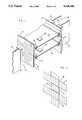
- FIG. 1is a view of an assembly of electronic circuit boards attached to the mounting boards, in a orthogonal arrangement.
- FIG. 2illustrates the electrical connections of the Zero Insertion Force connectors through the connection board.
- FIG. 3illustrates the local wiring arrangement for interconnecting pins that do not intersect with the connector on the outboard circuit boards to pins that will engage the connector.
- a first interconnection board 10is shown oriented in a vertical plane.
- the interconnection boardis populated with a plurality of pins 12 to which a circuit board connector 14 is connected or which are part of connector 14 and pins 13 to which a second, female circuit board connector 20 may be connected.
- a Zero Insertion Force (ZIF) card edge connector 14For example, on a first face 16 of the interconnection board 10 there is mounted a Zero Insertion Force (ZIF) card edge connector 14.
- the ZIP connector 14is of the type which is provided with pins 12 that can extend through the interconnection board 10 to expose the pins 12 on the second face 18 of interconnection board 10.
- the second face 18 of the interconnection board 10has pins 13 protruding therefrom.
- the pins 13are not a part of the ZIF connector 14 but rather are connected, by electrical conductors on or contained in interconnection board 10, to those pins 12 which are not plug connected to connector 20.
- the connection of pins 12 to pins 13will be described later with respect to FIG. 3.
- Connector 20is a conventional female connector with a plurality of rows of sockets oriented so the rows of sockets are vertical.
- the pins 12 which lie in the zone 42 which may be received by the sockets of connector 20coincide with the pin locations for some of the pins 12 extending through interconnection board 10 from the back of ZIF connector 14.
- Pins 12 which extend through the interconnection board 10 from the back of ZIF connector 14 but which are not within zone 42may be connected to pins 13 on an as needed basis to permit the conduction of signals between some of the pins 12 and pins 13. All of pins 13 lie within zone 42.
- circuit board 24Connected to connector 20 in a conventional manner is circuit board 24.
- a circuit board 24may be a signal board which receives signals in, for example, a fiber optical input form from a source external to the package described.
- the signalscould then be converted using an optical to electrical converter as are readily available commercially. Such optical to electrical converters are conventional and readily available commercially.
- the signals, once converted to electrical signalsare then conducted to the using device 26 on the circuit boards 28. Boards 28 are engaged by their edges 30 and the contacts thereon, by the ZIF connector 14.
- the utilizing device 26could be a crosspoint switching chip or a computer chip, or it could just as appropriately be a memory chip which may be accessible by processors which may reside on board 24. In any event, the number of interconnections between the input/output board 24 and the circuit board 28 may be significantly increased over the number of connections possible with non-orthogonal layout, and with minimal local board wiring.
- zone 42includes direct pin connections to boards 24 and 28 simultaneously.
- sixteen direct pin interconnectionsare available.
- the number of connections from the board 24 to board 28amounts to forty at each intersection of the circuit boards 24, 28.
- the pitch between adjacent boardscould be as close as one inch (25.4 mm). With pitches of one inch (25.4 mm), and 40 connections per square inch are achieved on the interconnection board 10.
- FIG. 1illustrates only two vertical boards 24 and two horizontal boards 28.
- the number of connectionsmay be increased to handle addition boards; for example, on a board having an edge dimension of four inches (10.16 cm) with boards connected on one inch (25.4 mm) intersection spacings, the number of connections possible are 640 in a 4 inch by 4 inch area. This number of connections may be doubled if the opposite side of each circuit board 28 is similarly mounted in a second ZIF connector 14 on a second interconnection board 10.
- a module measuring approximately 4 inches by 4 inches by 12 inchesis capable of having 1280 unique signal connections within the module.
- pin interconnectionsmay be used for voltage or ground connections between boards, simplifying the powering of the elements mounted to the various circuit boards.
- the ZIF connector 14 mounted on boards 10may advantageously be the type having a slot through which the board edge is inserted along a direction parallel to the axis of the ZIF connector 14. This permits insertion of and removal of boards 28 into and from the structure defined by the two parallel boards 10 when boards 10 are rigidly mounted.
- FIG. 2shows the connections of the ZIF connector 14 within boundary 40.
- the connections 12are arranged in four rows, equally spaced apart and protruding through the board 10.
- the pins 12 of the ZIF connector 14are positioned in the holes of the board 10 and soldered to complete the mounting of the ZIF connector 14.
- the pins 13protrude from the board in a pattern of typically four columns and occupying the area enclosed by boundary 42, between the connections of two adjacent ZIF connectors 14.
- Boundary 44encloses the connections that will be contacted by the female connector 20 of FIG. 1. It is seen that some of the connections protruding from ZIF connector 14 and the connections within boundary 42 are contacted by female connector 20.
- the connection pins that are common to the ZIF connector 14 and the female connector 20do not require further electrical connection to serve their intended purpose. However, the pin connections which are within boundary 40 and not within boundary 42 must be connected to the pin connections within boundary 42 in order for the electrical signals on one group of pins to be conveyed to the other group of pins.
- Conductors 50are formed in the board 10 during the board manufacture and may be positioned to connect pins of one of the groups to a pin in another of the groups of non-common pin connections. For example, a pin 12 in one group may be connected to a pin 13 in another group by a conductor 50 as shown in FIG. 3. Conductors 50 are laid out with a desire to maintain all connections between non-common pins approximately equal. Conductors 52 are examples of a layout connecting pins 12 and 13 on board 10 when the length of the conductors relative to each other is not a critical consideration. Should it become necessary to lay out very intricate patterns of conductors to property connect selected ones of pins 12 with selected ones of pins 13, multiple layers of conductors may be formed and separated by insulating layers as is well known in the circuit board art.
- ZIF connectors 14 and female connectors 20are described for illustrative purposes and that all connections of the board 10 could be made with ZIF connectors or by female connectors. Such connectors limit to some extent the flexibility of the design.
- the combination of ZIF connectors 14 and female connectors 20is the preferred design.
- the female connectors 20have been shown as pin into socket type connectors but it should be recognized that a ZIF connector could be substituted; the connector could also be of the surface mount type where the board 10 would be provided with solder pads rather than pins 13 for engaging the ZIF connector.
- a third edge of circuit board 28, preferably the leading edge as board 28 is inserted into the connectors 14,may be contacted by conventional connectors to provide power or signal connections to the circuit board 28. If air circulation is not required for cooling the components 26, an interconnection board 10 can be added to the back of the arrangement shown in FIG. 1 to further expand the interconnection capability between circuit board 28 and circuit boards 24 or their counterparts.
Landscapes
- Engineering & Computer Science (AREA)
- Microelectronics & Electronic Packaging (AREA)
- Coupling Device And Connection With Printed Circuit (AREA)
- Combinations Of Printed Boards (AREA)
Abstract
Description
The invention relates to the packaging of electronic circuits, and particularly to the interconnecting of the electronic circuits to other devices and circuits which require large numbers of interconnections. The invention is particularly useful in the area of crosspoint switching or to the area of parallel processing where several computer processors require access to the same switch network, memory or other system resource.
When large numbers of unique signal connections are required to interconnect the elements of an electrical network, such as the signal inputs and outputs of crosspoint switch elements or devices, the connection of the inputs and outputs to the switch device can require extensive circuit board complexity and interconnection distance design to provide the conductor paths on the circuit board necessary to make the interconnections. Further complications result from the requirement that in many cases, conductor paths between related inputs and connections to the crosspoint switching device be of equal length to make sure that all signals reaching the switching device are delayed by approximately the same amount of time.
This requirement for large numbers of unique signals exists in several environments but is very prevalent in the area of parallel processing. When a computer is comprised of several processors operating simultaneously, the signals to and from each other or shared memory through a switch network necessitates many point-to-point connections and must all be timed to arrive at the receiving device at approximately the same time, and all the processors must be able to access the memory which is common to all processors.
The cost of the interconnection of the crosspoint switching chips or devices to the input and output signal boards can become a significant cost element in an overall system.
U.S. Pat. No. 3,368,155, to N. E. Hoffman addresses the need to package several circuit boards in a module. This approach does not address the need for large numbers of unique signals needed in the environment of the invention.
U.S. Pat. No. 4,401,351 to G. C. Record discloses a card cage approach to interconnecting several circuit boards to a mother board, but fails to disclose a further interconnection by orthogonal plugging of other boards. Mother boards in adjacent cages are connected by a coupling means.
U.S. Pat. No. 4,490,000 to J. C. Asick et al discloses a device for interconnecting two adjacent parallel circuit boards but does not disclose the orthogonal interconnection of circuit boards.
U.S. Pat. No. 4,582,386 to J. D. Martins discloses a circuit board connector which provides electrical connections to a mating connector portion which has a pattern of four rows of pins uniformly spaced. Another example of a connector having receptors for pins and having multiple rows of receptors is U.S. Pat. No. 4,932,885 to J. P. Scholz.
It is an object of the invention to greatly increase the efficiency of making large numbers of interconnections between circuit boards.
It is a further object of the invention to reduce the need for designing large interconnection schemes for connecting circuit boards.
It is another object of the invention to make the interconnections between the connected circuit boards with a minimum of length of conductors.
The shortcomings of the prior art are overcome and the objects of the invention accomplished by the invention, a better understanding of which thereof may be had from the attached drawings and reference to the detailed description of the invention to follow.
FIG. 1 is a view of an assembly of electronic circuit boards attached to the mounting boards, in a orthogonal arrangement.
FIG. 2 illustrates the electrical connections of the Zero Insertion Force connectors through the connection board.
FIG. 3 illustrates the local wiring arrangement for interconnecting pins that do not intersect with the connector on the outboard circuit boards to pins that will engage the connector.
Referring to FIG. 1, afirst interconnection board 10 is shown oriented in a vertical plane. The interconnection board is populated with a plurality ofpins 12 to which acircuit board connector 14 is connected or which are part ofconnector 14 andpins 13 to which a second, femalecircuit board connector 20 may be connected. For example, on afirst face 16 of theinterconnection board 10 there is mounted a Zero Insertion Force (ZIF)card edge connector 14. TheZIP connector 14 is of the type which is provided withpins 12 that can extend through theinterconnection board 10 to expose thepins 12 on thesecond face 18 ofinterconnection board 10. In addition to thepins 12 directly in electrical communication with contacts of theZIP connector 14, thesecond face 18 of theinterconnection board 10 haspins 13 protruding therefrom. Thepins 13 are not a part of theZIF connector 14 but rather are connected, by electrical conductors on or contained ininterconnection board 10, to thosepins 12 which are not plug connected toconnector 20. The connection ofpins 12 topins 13 will be described later with respect to FIG. 3.
Connected toconnector 20 in a conventional manner iscircuit board 24. If used to package fiber-optic crosspoint switches, for example, acircuit board 24 may be a signal board which receives signals in, for example, a fiber optical input form from a source external to the package described. The signals could then be converted using an optical to electrical converter as are readily available commercially. Such optical to electrical converters are conventional and readily available commercially. The signals, once converted to electrical signals are then conducted to the usingdevice 26 on thecircuit boards 28.Boards 28 are engaged by their edges 30 and the contacts thereon, by theZIF connector 14. The utilizingdevice 26 could be a crosspoint switching chip or a computer chip, or it could just as appropriately be a memory chip which may be accessible by processors which may reside onboard 24. In any event, the number of interconnections between the input/output board 24 and thecircuit board 28 may be significantly increased over the number of connections possible with non-orthogonal layout, and with minimal local board wiring.
The orthogonal arrangement ofboard 24, andboard 10 andboard 28 permits the connection ofboard 24 tomultiple boards 28 without long runs of local board wiring. Referring to FIG. 3,zone 42 includes direct pin connections toboards interconnection board 10 and the use of a four row pin arrangement on theZIF connector 14 and on theconnector 20, at each intersection of the plane ofboard 24 with the plane ofboard 28, sixteen direct pin interconnections are available. By including three adjacent columns ofpins 12 on either side of zone 22 and three rows ofpins 13 above and below thepins 12 extending directly fromZIF connector 14 through the board, the number of connections from theboard 24 to board 28 amounts to forty at each intersection of thecircuit boards
Assuming that a uniform pin spacing of 0.100 inches (2.54 mm), a common standard in pin connection technology, is used, the pitch between adjacent boards could be as close as one inch (25.4 mm). With pitches of one inch (25.4 mm), and 40 connections per square inch are achieved on theinterconnection board 10.
FIG. 1 illustrates only twovertical boards 24 and twohorizontal boards 28. By lengthening the boards, the number of connections may be increased to handle addition boards; for example, on a board having an edge dimension of four inches (10.16 cm) with boards connected on one inch (25.4 mm) intersection spacings, the number of connections possible are 640 in a 4 inch by 4 inch area. This number of connections may be doubled if the opposite side of eachcircuit board 28 is similarly mounted in asecond ZIF connector 14 on asecond interconnection board 10.
Accordingly, a module measuring approximately 4 inches by 4 inches by 12 inches is capable of having 1280 unique signal connections within the module.
Some of the pin interconnections may be used for voltage or ground connections between boards, simplifying the powering of the elements mounted to the various circuit boards.
Referring to FIG. 1, theZIF connector 14 mounted onboards 10 may advantageously be the type having a slot through which the board edge is inserted along a direction parallel to the axis of theZIF connector 14. This permits insertion of and removal ofboards 28 into and from the structure defined by the twoparallel boards 10 whenboards 10 are rigidly mounted.
FIG. 2 shows the connections of theZIF connector 14 withinboundary 40. Theconnections 12 are arranged in four rows, equally spaced apart and protruding through theboard 10. Thepins 12 of theZIF connector 14 are positioned in the holes of theboard 10 and soldered to complete the mounting of theZIF connector 14. Thepins 13 protrude from the board in a pattern of typically four columns and occupying the area enclosed byboundary 42, between the connections of twoadjacent ZIF connectors 14.
In order to connect the non-connected pins ofZIF connector 14 to the non-connected pins that engagefemale connector 20, local wiring must be accomplished. The local wiring is formed by conventional printed circuit board fabrication techniques.Conductors 50 are formed in theboard 10 during the board manufacture and may be positioned to connect pins of one of the groups to a pin in another of the groups of non-common pin connections. For example, apin 12 in one group may be connected to apin 13 in another group by aconductor 50 as shown in FIG. 3.Conductors 50 are laid out with a desire to maintain all connections between non-common pins approximately equal.Conductors 52 are examples of alayout connecting pins board 10 when the length of the conductors relative to each other is not a critical consideration. Should it become necessary to lay out very intricate patterns of conductors to property connect selected ones ofpins 12 with selected ones ofpins 13, multiple layers of conductors may be formed and separated by insulating layers as is well known in the circuit board art.
It should be understood that the use ofZIF connectors 14 andfemale connectors 20 are described for illustrative purposes and that all connections of theboard 10 could be made with ZIF connectors or by female connectors. Such connectors limit to some extent the flexibility of the design. The combination ofZIF connectors 14 andfemale connectors 20 is the preferred design.
While the local wiring ofboard 10 is preferably accomplished as described above, it should be understood that this structure is also conducive to wire wrap interconnections and thus is useful in early level prototype designs. After the interconnections have proven to be as desired, the wiring approach may then give way to the local wiring of the circuit board during its manufacture and the total enclosure of the conductors within the board.
Thefemale connectors 20 have been shown as pin into socket type connectors but it should be recognized that a ZIF connector could be substituted; the connector could also be of the surface mount type where theboard 10 would be provided with solder pads rather thanpins 13 for engaging the ZIF connector.
From the foregoing description and explanation, it is appreciated that a third edge ofcircuit board 28, preferably the leading edge asboard 28 is inserted into theconnectors 14, may be contacted by conventional connectors to provide power or signal connections to thecircuit board 28. If air circulation is not required for cooling thecomponents 26, aninterconnection board 10 can be added to the back of the arrangement shown in FIG. 1 to further expand the interconnection capability betweencircuit board 28 andcircuit boards 24 or their counterparts.
Further, it should be understood that modifications and changes may be made by one of skill in the art to the preferred embodiment without departing from the scope of the invention.
Claims (3)
1. A high density packaging system for interconnecting a plurality of circuit cards, said plurality of circuit cards comprising at least a first set, a second set and a third set of said circuit cards;
said circuit cards comprising electrical components, wherein said first set of said circuit cards comprises first electrical connectors disposed along a first edge of said circuit cards of said first set and, wherein said third set of said circuit cards comprises a first plurality of electrical connectors disposed along a first edge of said circuit cards of said third set, and wherein said second set of said circuit cards comprises a first plurality of electrical connection points disposed along at least two edges of each of said cards of said second set, said edges being parallel and disposed on opposite edges of said cards;
said first plurality of electrical connectors and said first plurality of electrical connectors and said first plurality of electrical connection points being electrically connected to at least some of said electrical components on said plurality of said circuit cards;
a first interconnection circuit board disposed intermediate said first set of said circuit cards and said second set of said circuit cards;
a second interconnection circuit board disposed intermediate said second set of said circuit cards and said third set of said circuit cards;
said first and second interconnection circuit boards each disposed parallel to the other and a first surface of said first interconnection circuit board facing toward a first surface of the second interconnection circuit board;
a second plurality of connectors disposed on said first surface of each of said interconnection circuit boards, said second plurality of connectors being zero insertion force connectors with an insertion axis parallel to a long axis of said zero insertion force connectors;
a second plurality of connection points disposed on a second surface of each of said interconnection circuit boards opposite said first surfaces of said interconnection circuit boards, said second plurality of connection points disposed to engage said first plurality of electrical connectors of said first set of circuit cards and said third set of circuit cards, when said first set and said third set of circuit cards are oriented orthogonally with respect to said second set of circuit cards; and
electrical interconnection paths, including said plurality of connection points connecting each of said first connectors to at least one of said plurality of said second connectors located on said first surface of said first and second interconnection boards;
whereby individual ones of said second set of circuit cards are inserted into said at least two of said second plurality of connectors to establish contact with said circuit cards of said first set and circuit cards of said third set without having to disturb the spatial spacing of said interconnection circuit cards.
2. The packaging system of claim 1 wherein said plurality of first connectors comprise zero insertion force connectors having an insertion axis parallel to a long axis of said connector and parallel to an edge of one of said circuit cards of said second set.
3. A method of interconnecting a first set of circuit cards and a third set of circuit cards with a second set of circuit cards, comprising the steps of:
providing at least two interconnection circuit boards, each having at least first and second parallel faces;
positioning said interconnection circuit boards parallel to and spaced from each other;
providing on at least a first face of each said interconnection board a plurality of zero insertion force connectors having an insertion axis parallel to said first face of said interconnection board, each said connector disposed parallel to all said connectors;
providing a plurality of electrical connection points on said second face of each of said interconnection boards;
disposing a first plurality of circuit cards in electrical connection with said electrical connection points on said second face of each of said interconnection cards and disposed orthogonally with respect to said zero insertion force connectors;
inserting at least a second plurality of circuit cards into said zero insertion force connectors along said insertion axes with each said card of said second plurality of circuit cards disposed with two opposing edges each within a zero insertion force connector, one said zero insertion force connector residing on each of said interconnection circuit boards;
whereby each of said first plurality of circuit cards is electrically connected with said second plurality of circuit cards.
Priority Applications (4)
| Application Number | Priority Date | Filing Date | Title |
|---|---|---|---|
| US07/827,240US5335146A (en) | 1992-01-29 | 1992-01-29 | High density packaging for device requiring large numbers of unique signals utilizing orthogonal plugging and zero insertion force connetors |
| JP4329343AJPH07111891B2 (en) | 1992-01-29 | 1992-12-09 | Packaging system |
| DE69304359TDE69304359D1 (en) | 1992-01-29 | 1993-01-27 | Assembly arrangement |
| EP93300600AEP0554077B1 (en) | 1992-01-29 | 1993-01-27 | Packaging system |
Applications Claiming Priority (1)
| Application Number | Priority Date | Filing Date | Title |
|---|---|---|---|
| US07/827,240US5335146A (en) | 1992-01-29 | 1992-01-29 | High density packaging for device requiring large numbers of unique signals utilizing orthogonal plugging and zero insertion force connetors |
Publications (1)
| Publication Number | Publication Date |
|---|---|
| US5335146Atrue US5335146A (en) | 1994-08-02 |
Family
ID=25248684
Family Applications (1)
| Application Number | Title | Priority Date | Filing Date |
|---|---|---|---|
| US07/827,240Expired - Fee RelatedUS5335146A (en) | 1992-01-29 | 1992-01-29 | High density packaging for device requiring large numbers of unique signals utilizing orthogonal plugging and zero insertion force connetors |
Country Status (4)
| Country | Link |
|---|---|
| US (1) | US5335146A (en) |
| EP (1) | EP0554077B1 (en) |
| JP (1) | JPH07111891B2 (en) |
| DE (1) | DE69304359D1 (en) |
Cited By (58)
| Publication number | Priority date | Publication date | Assignee | Title |
|---|---|---|---|---|
| WO1999011104A1 (en)* | 1997-08-28 | 1999-03-04 | Ascend Communications, Inc. | Electronic interconnection method and apparatus for minimizing propagation delays |
| WO2000069233A1 (en)* | 1999-05-05 | 2000-11-16 | Nokia Networks Oy | Arrangement, method and positioning board in a rack of a cross connect node |
| US6344975B1 (en)* | 1999-08-30 | 2002-02-05 | Lucent Technologies Inc. | Modular backplane |
| US6392142B1 (en)* | 1998-04-28 | 2002-05-21 | Fujitsu Limited | Printed wiring board mounting structure |
| US6477059B1 (en)* | 1999-08-27 | 2002-11-05 | Sony Computer Entertainment, Inc | Board connection structure, electronic device with board connection structure and connector used therein |
| US20020182926A1 (en)* | 1999-02-26 | 2002-12-05 | Micron Technology, Inc. | Apparatus and method for packaging circuits |
| US20020182899A1 (en)* | 2001-05-29 | 2002-12-05 | International Business Machines Corporation | Fragmented backplane system for I/O applications |
| US6540522B2 (en) | 2001-04-26 | 2003-04-01 | Tyco Electronics Corporation | Electrical connector assembly for orthogonally mating circuit boards |
| US20030137817A1 (en)* | 2002-01-18 | 2003-07-24 | Volstorf James R. | Electrical connection system for two printed circuit boards mounted on opposite sides of a mid-plane printed circuit board at angles to each other |
| US6607401B1 (en)* | 1999-01-28 | 2003-08-19 | Berg Technology, Inc. | Electrical connector mateable in a plurality of orientations |
| US20030224645A1 (en)* | 2002-05-31 | 2003-12-04 | Racksaver, Inc. | Rack mountable computer component power distribution unit and method |
| US20030223193A1 (en)* | 2002-05-31 | 2003-12-04 | Racksaver, Inc. | Method and apparatus for rack mounting computer components |
| US6690584B2 (en)* | 2000-08-14 | 2004-02-10 | Fujitsu Limited | Information-processing device having a crossbar-board connected to back panels on different sides |
| US6705895B2 (en) | 2002-04-25 | 2004-03-16 | Tyco Electronics Corporation | Orthogonal interface for connecting circuit boards carrying differential pairs |
| US20040126065A1 (en)* | 2002-12-31 | 2004-07-01 | Levy Paul S. | Module interface with optical and electrical interconnects |
| US20050047819A1 (en)* | 2003-09-01 | 2005-03-03 | Canon Kabushiki Kaisha | Electronic apparatus having a plurality of circuit substrates |
| US20050117317A1 (en)* | 2003-11-28 | 2005-06-02 | Warburton Kenneth J. | Bridged parallel distributing frame |
| US20050207134A1 (en)* | 2004-03-16 | 2005-09-22 | Belady Christian L | Cell board interconnection architecture |
| US20060024984A1 (en)* | 2004-07-01 | 2006-02-02 | Cohen Thomas S | Midplane especially applicable to an orthogonal architecture electronic system |
| US20060073709A1 (en)* | 2004-10-06 | 2006-04-06 | Teradyne, Inc. | High density midplane |
| US20060171133A1 (en)* | 2005-02-03 | 2006-08-03 | Fujitsu Network Communications, Inc. | Grow as you go equipment shelf |
| USD527060S1 (en) | 2004-03-22 | 2006-08-22 | Nautilus, Inc. | Exercise device with treadles |
| US7097593B2 (en) | 2003-08-11 | 2006-08-29 | Nautilus, Inc. | Combination of treadmill and stair climbing machine |
| US20070059961A1 (en)* | 2005-06-30 | 2007-03-15 | Cartier Marc B | Electrical connector for interconnection assembly |
| US7239528B1 (en)* | 2005-10-05 | 2007-07-03 | Cisco Technology, Inc. | Techniques for accommodating variations in chassis tolerances |
| US7298625B1 (en)* | 2007-01-17 | 2007-11-20 | Inventec Corporation | Expansion structure of memory module slot |
| US20080026638A1 (en)* | 2004-07-01 | 2008-01-31 | Cohen Thomas S | Differential electrical connector assembly |
| US20080225474A1 (en)* | 2006-12-06 | 2008-09-18 | David Flynn | Apparatus, system, and method for scalable, composite, reconfigurable backplane |
| US7455626B2 (en) | 2001-12-31 | 2008-11-25 | Nautilus, Inc. | Treadmill |
| US20090034216A1 (en)* | 2007-07-31 | 2009-02-05 | Christian Petersen | Low profile dimm board |
| US20090040740A1 (en)* | 2007-08-09 | 2009-02-12 | Mc Technology Gmbh | Wiring circuit board |
| US20090122500A1 (en)* | 2007-11-12 | 2009-05-14 | Metzger Thomas R | Card Level Enclosure System Having Enhanced Thermal Transfer And Improved EMI Characteristics |
| US20090225527A1 (en)* | 2008-03-06 | 2009-09-10 | Sun Microsystems, Inc. | Multi-function mezzanine board alignment and mounting device, with integrated handle |
| USRE42698E1 (en) | 2001-07-25 | 2011-09-13 | Nautilus, Inc. | Treadmill having dual treads for stepping exercises |
| US8444436B1 (en) | 2004-07-01 | 2013-05-21 | Amphenol Corporation | Midplane especially applicable to an orthogonal architecture electronic system |
| US8491313B2 (en) | 2011-02-02 | 2013-07-23 | Amphenol Corporation | Mezzanine connector |
| US20140094063A1 (en)* | 2012-09-28 | 2014-04-03 | Gregory M. Daly | System, circuit module, and circuit module connector |
| US8864521B2 (en) | 2005-06-30 | 2014-10-21 | Amphenol Corporation | High frequency electrical connector |
| US20150049422A1 (en)* | 2012-05-14 | 2015-02-19 | Zte Corporation | ATCA Backplane |
| DE102013217270A1 (en)* | 2013-08-29 | 2015-03-05 | Zf Friedrichshafen Ag | Printed circuit board device with a plug contact |
| US20160066436A1 (en)* | 2014-09-01 | 2016-03-03 | Quanta Computer Inc. | Method for fabricating circuit board structure |
| US20160286648A1 (en)* | 2013-06-26 | 2016-09-29 | E Ink Holdings Inc. | Electronic apparatus |
| US10034376B2 (en)* | 2016-08-16 | 2018-07-24 | Lite-On Electronics (Guangzhou) Limited | Internal/external circuit board connection structure |
| US10109959B1 (en)* | 2017-05-25 | 2018-10-23 | Juniper Networks, Inc. | Electrical connector with embedded processor |
| US11444397B2 (en) | 2015-07-07 | 2022-09-13 | Amphenol Fci Asia Pte. Ltd. | Electrical connector with cavity between terminals |
| US11469554B2 (en) | 2020-01-27 | 2022-10-11 | Fci Usa Llc | High speed, high density direct mate orthogonal connector |
| US11522310B2 (en) | 2012-08-22 | 2022-12-06 | Amphenol Corporation | High-frequency electrical connector |
| US11539171B2 (en) | 2016-08-23 | 2022-12-27 | Amphenol Corporation | Connector configurable for high performance |
| US11652020B2 (en)* | 2019-05-29 | 2023-05-16 | Intel Corporation | Thermal solutions for multi-package assemblies and methods for fabricating the same |
| US11715914B2 (en) | 2014-01-22 | 2023-08-01 | Amphenol Corporation | High speed, high density electrical connector with shielded signal paths |
| US11757224B2 (en) | 2010-05-07 | 2023-09-12 | Amphenol Corporation | High performance cable connector |
| US11757215B2 (en) | 2018-09-26 | 2023-09-12 | Amphenol East Asia Electronic Technology (Shenzhen) Co., Ltd. | High speed electrical connector and printed circuit board thereof |
| US11799246B2 (en) | 2020-01-27 | 2023-10-24 | Fci Usa Llc | High speed connector |
| US11817655B2 (en) | 2020-09-25 | 2023-11-14 | Amphenol Commercial Products (Chengdu) Co., Ltd. | Compact, high speed electrical connector |
| US11942716B2 (en) | 2020-09-22 | 2024-03-26 | Amphenol Commercial Products (Chengdu) Co., Ltd. | High speed electrical connector |
| US20240314930A1 (en)* | 2023-03-14 | 2024-09-19 | Samsung Electronics Co., Ltd. | Computing system with connecting boards |
| US12300920B2 (en) | 2021-08-13 | 2025-05-13 | Amphenol Commercial Products (Chengdu) Co., Ltd. | High performance card edge connector for high bandwidth transmission |
| US12300936B2 (en) | 2019-02-19 | 2025-05-13 | Amphenol Corporation | High speed connector |
Families Citing this family (4)
| Publication number | Priority date | Publication date | Assignee | Title |
|---|---|---|---|---|
| DE19945141A1 (en)* | 1999-09-21 | 2001-01-11 | Siemens Ag | Module frame for multiprocessor system |
| JP3759870B2 (en)* | 2000-10-27 | 2006-03-29 | 住友電装株式会社 | connector |
| JP2015035546A (en)* | 2013-08-09 | 2015-02-19 | 東芝シュネデール・インバータ株式会社 | Print circuit board |
| CN109788697B (en)* | 2018-12-04 | 2021-04-09 | 华为技术有限公司 | Electronic devices and storage devices with parallel backplanes |
Citations (27)
| Publication number | Priority date | Publication date | Assignee | Title |
|---|---|---|---|---|
| US3368115A (en)* | 1965-10-19 | 1968-02-06 | Amp Inc | Modular housing for integrated circuit structure with improved interconnection means |
| GB1313641A (en)* | 1971-09-28 | 1973-04-18 | Ncr Co | Electrical connector for printed circuit cards |
| DE2320202A1 (en)* | 1973-04-19 | 1974-11-07 | Siemens Ag | ARRANGEMENT FOR THE ALTERNATE ELECTRICAL CONNECTION OF A MULTIPLE NUMBER OF COMPONENT CARRIERS (E.G. OF PRINTED CIRCUIT BOARDS) |
| US4232924A (en)* | 1978-10-23 | 1980-11-11 | Nanodata Corporation | Circuit card adapter |
| US4266839A (en)* | 1979-07-06 | 1981-05-12 | E. I. Du Pont De Nemours And Company | Zero insertion force toggle link connector |
| US4401351A (en)* | 1981-09-28 | 1983-08-30 | Advant Corporation | Expandable card cage |
| WO1983004466A1 (en)* | 1982-06-07 | 1983-12-22 | Transpath, Limited | Tiered orthogonal related 3-d printed boards circuit |
| US4451107A (en)* | 1982-08-23 | 1984-05-29 | Amp Incorporated | High speed modular connector for printed circuit boards |
| US4490000A (en)* | 1983-03-23 | 1984-12-25 | Amp Incorporated | Multi-plane crossover contact |
| US4498717A (en)* | 1983-08-29 | 1985-02-12 | Gte Communication Systems Corp. | Printed wiring board interconnect arrangement |
| SU1193847A1 (en)* | 1984-02-14 | 1985-11-23 | Lev V Rylov | Case for electronic equipment |
| US4582386A (en)* | 1984-11-01 | 1986-04-15 | Elfab Corp. | Connector with enlarged power contact |
| US4603928A (en)* | 1985-03-20 | 1986-08-05 | Amp Incorporated | Board to board edge connector |
| US4613193A (en)* | 1984-08-13 | 1986-09-23 | Tritec, Inc. | Board-operated electrical connector for printed circuit boards |
| US4631637A (en)* | 1985-12-23 | 1986-12-23 | Burroughs Corporation | Dual backplane interconnect system |
| US4703394A (en)* | 1985-10-25 | 1987-10-27 | Alcatel | System for interconnecting orthogonally disposed printed circuit boards and switching networks employing same |
| US4744006A (en)* | 1986-07-10 | 1988-05-10 | Duffield Robert H | Apparatus for expanding the input/output capabilities of a personal computer |
| US4815979A (en)* | 1987-12-23 | 1989-03-28 | Ncr Corporation | Right angle electrical connector with or without wiping action |
| US4838798A (en)* | 1988-06-15 | 1989-06-13 | Amp Incorporated | High density board to board interconnection system |
| US4863395A (en)* | 1989-01-17 | 1989-09-05 | Robert Babuka | Zero insertion force connector with component card |
| US4876630A (en)* | 1987-06-22 | 1989-10-24 | Reliance Comm/Tec Corporation | Mid-plane board and assembly therefor |
| US4907977A (en)* | 1988-10-14 | 1990-03-13 | Ncr Corporation | Computer backpanel inversion coupler |
| US4932885A (en)* | 1989-06-29 | 1990-06-12 | Amp Corporation | High density connector |
| US4936785A (en)* | 1988-12-19 | 1990-06-26 | Krug Eric M | Interchangeable adapter module for electronic devices |
| US5091822A (en)* | 1989-06-15 | 1992-02-25 | Graphico Co., Ltd. | Radial type of parallel system bus structure with printed, twisted conductor lines |
| US5119273A (en)* | 1990-01-29 | 1992-06-02 | The United States Of America As Represented By The Secretary Of The Navy | High speed parallel backplane |
| US5211565A (en)* | 1990-11-27 | 1993-05-18 | Cray Research, Inc. | High density interconnect apparatus |
Family Cites Families (2)
| Publication number | Priority date | Publication date | Assignee | Title |
|---|---|---|---|---|
| JPS5255946U (en)* | 1975-10-15 | 1977-04-22 | ||
| DE2943942A1 (en)* | 1979-10-31 | 1981-05-14 | Michael Dr.med. Dr.rer.nat. 6800 Mannheim Scherz | METHOD AND DEVICE FOR THE EXAMINATION OF SUBSTANCES AND SUBSTANCE MIXTURES |
- 1992
- 1992-01-29USUS07/827,240patent/US5335146A/ennot_activeExpired - Fee Related
- 1992-12-09JPJP4329343Apatent/JPH07111891B2/ennot_activeExpired - Lifetime
- 1993
- 1993-01-27EPEP93300600Apatent/EP0554077B1/ennot_activeExpired - Lifetime
- 1993-01-27DEDE69304359Tpatent/DE69304359D1/ennot_activeExpired - Lifetime
Patent Citations (27)
| Publication number | Priority date | Publication date | Assignee | Title |
|---|---|---|---|---|
| US3368115A (en)* | 1965-10-19 | 1968-02-06 | Amp Inc | Modular housing for integrated circuit structure with improved interconnection means |
| GB1313641A (en)* | 1971-09-28 | 1973-04-18 | Ncr Co | Electrical connector for printed circuit cards |
| DE2320202A1 (en)* | 1973-04-19 | 1974-11-07 | Siemens Ag | ARRANGEMENT FOR THE ALTERNATE ELECTRICAL CONNECTION OF A MULTIPLE NUMBER OF COMPONENT CARRIERS (E.G. OF PRINTED CIRCUIT BOARDS) |
| US4232924A (en)* | 1978-10-23 | 1980-11-11 | Nanodata Corporation | Circuit card adapter |
| US4266839A (en)* | 1979-07-06 | 1981-05-12 | E. I. Du Pont De Nemours And Company | Zero insertion force toggle link connector |
| US4401351A (en)* | 1981-09-28 | 1983-08-30 | Advant Corporation | Expandable card cage |
| WO1983004466A1 (en)* | 1982-06-07 | 1983-12-22 | Transpath, Limited | Tiered orthogonal related 3-d printed boards circuit |
| US4451107A (en)* | 1982-08-23 | 1984-05-29 | Amp Incorporated | High speed modular connector for printed circuit boards |
| US4490000A (en)* | 1983-03-23 | 1984-12-25 | Amp Incorporated | Multi-plane crossover contact |
| US4498717A (en)* | 1983-08-29 | 1985-02-12 | Gte Communication Systems Corp. | Printed wiring board interconnect arrangement |
| SU1193847A1 (en)* | 1984-02-14 | 1985-11-23 | Lev V Rylov | Case for electronic equipment |
| US4613193A (en)* | 1984-08-13 | 1986-09-23 | Tritec, Inc. | Board-operated electrical connector for printed circuit boards |
| US4582386A (en)* | 1984-11-01 | 1986-04-15 | Elfab Corp. | Connector with enlarged power contact |
| US4603928A (en)* | 1985-03-20 | 1986-08-05 | Amp Incorporated | Board to board edge connector |
| US4703394A (en)* | 1985-10-25 | 1987-10-27 | Alcatel | System for interconnecting orthogonally disposed printed circuit boards and switching networks employing same |
| US4631637A (en)* | 1985-12-23 | 1986-12-23 | Burroughs Corporation | Dual backplane interconnect system |
| US4744006A (en)* | 1986-07-10 | 1988-05-10 | Duffield Robert H | Apparatus for expanding the input/output capabilities of a personal computer |
| US4876630A (en)* | 1987-06-22 | 1989-10-24 | Reliance Comm/Tec Corporation | Mid-plane board and assembly therefor |
| US4815979A (en)* | 1987-12-23 | 1989-03-28 | Ncr Corporation | Right angle electrical connector with or without wiping action |
| US4838798A (en)* | 1988-06-15 | 1989-06-13 | Amp Incorporated | High density board to board interconnection system |
| US4907977A (en)* | 1988-10-14 | 1990-03-13 | Ncr Corporation | Computer backpanel inversion coupler |
| US4936785A (en)* | 1988-12-19 | 1990-06-26 | Krug Eric M | Interchangeable adapter module for electronic devices |
| US4863395A (en)* | 1989-01-17 | 1989-09-05 | Robert Babuka | Zero insertion force connector with component card |
| US5091822A (en)* | 1989-06-15 | 1992-02-25 | Graphico Co., Ltd. | Radial type of parallel system bus structure with printed, twisted conductor lines |
| US4932885A (en)* | 1989-06-29 | 1990-06-12 | Amp Corporation | High density connector |
| US5119273A (en)* | 1990-01-29 | 1992-06-02 | The United States Of America As Represented By The Secretary Of The Navy | High speed parallel backplane |
| US5211565A (en)* | 1990-11-27 | 1993-05-18 | Cray Research, Inc. | High density interconnect apparatus |
Cited By (114)
| Publication number | Priority date | Publication date | Assignee | Title |
|---|---|---|---|---|
| US6015300A (en)* | 1997-08-28 | 2000-01-18 | Ascend Communications, Inc. | Electronic interconnection method and apparatus for minimizing propagation delays |
| WO1999011104A1 (en)* | 1997-08-28 | 1999-03-04 | Ascend Communications, Inc. | Electronic interconnection method and apparatus for minimizing propagation delays |
| US6392142B1 (en)* | 1998-04-28 | 2002-05-21 | Fujitsu Limited | Printed wiring board mounting structure |
| US6607401B1 (en)* | 1999-01-28 | 2003-08-19 | Berg Technology, Inc. | Electrical connector mateable in a plurality of orientations |
| US20020182926A1 (en)* | 1999-02-26 | 2002-12-05 | Micron Technology, Inc. | Apparatus and method for packaging circuits |
| US6537100B2 (en)* | 1999-02-26 | 2003-03-25 | Micron Technology, Inc. | Apparatus and method for packaging circuits |
| WO2000069233A1 (en)* | 1999-05-05 | 2000-11-16 | Nokia Networks Oy | Arrangement, method and positioning board in a rack of a cross connect node |
| US6477059B1 (en)* | 1999-08-27 | 2002-11-05 | Sony Computer Entertainment, Inc | Board connection structure, electronic device with board connection structure and connector used therein |
| US6344975B1 (en)* | 1999-08-30 | 2002-02-05 | Lucent Technologies Inc. | Modular backplane |
| US20040150964A1 (en)* | 2000-08-14 | 2004-08-05 | Fujitsu Limited | Information-processing device having a crossbar-board connected to back panels on different sides |
| US7193861B2 (en)* | 2000-08-14 | 2007-03-20 | Fujitsu Limited | Information-processing device having a crossbar-board connected to back panels on different sides |
| US7133292B2 (en)* | 2000-08-14 | 2006-11-07 | Fujitsu Limited | Information-processing device having a crossbar-board connected to back panels on different sides |
| US20040150965A1 (en)* | 2000-08-14 | 2004-08-05 | Fujitsu Limited | Information-processing device having a crossbar-board connected to back panels on different sides |
| US6690584B2 (en)* | 2000-08-14 | 2004-02-10 | Fujitsu Limited | Information-processing device having a crossbar-board connected to back panels on different sides |
| US6540522B2 (en) | 2001-04-26 | 2003-04-01 | Tyco Electronics Corporation | Electrical connector assembly for orthogonally mating circuit boards |
| US20020182899A1 (en)* | 2001-05-29 | 2002-12-05 | International Business Machines Corporation | Fragmented backplane system for I/O applications |
| US6932617B2 (en) | 2001-05-29 | 2005-08-23 | International Business Machines Corporation | Fragmented backplane system for I/O applications |
| US6824393B2 (en)* | 2001-05-29 | 2004-11-30 | International Business Machines Corporation | Fragmented backplane system for I/O applications |
| USRE42698E1 (en) | 2001-07-25 | 2011-09-13 | Nautilus, Inc. | Treadmill having dual treads for stepping exercises |
| US7544153B2 (en) | 2001-12-31 | 2009-06-09 | Nautilus, Inc. | Treadmill |
| US7455626B2 (en) | 2001-12-31 | 2008-11-25 | Nautilus, Inc. | Treadmill |
| US6717825B2 (en) | 2002-01-18 | 2004-04-06 | Fci Americas Technology, Inc. | Electrical connection system for two printed circuit boards mounted on opposite sides of a mid-plane printed circuit board at angles to each other |
| US20030137817A1 (en)* | 2002-01-18 | 2003-07-24 | Volstorf James R. | Electrical connection system for two printed circuit boards mounted on opposite sides of a mid-plane printed circuit board at angles to each other |
| US6705895B2 (en) | 2002-04-25 | 2004-03-16 | Tyco Electronics Corporation | Orthogonal interface for connecting circuit boards carrying differential pairs |
| US6836030B2 (en)* | 2002-05-31 | 2004-12-28 | Verari Systems, Inc. | Rack mountable computer component power distribution unit and method |
| US20050083651A1 (en)* | 2002-05-31 | 2005-04-21 | Smith John V. | Method and apparatus for rack mounting computer components |
| US7420805B2 (en) | 2002-05-31 | 2008-09-02 | Verari Systems, Inc. | Method and apparatus for rack mounting computer components |
| US20030224645A1 (en)* | 2002-05-31 | 2003-12-04 | Racksaver, Inc. | Rack mountable computer component power distribution unit and method |
| US20030223193A1 (en)* | 2002-05-31 | 2003-12-04 | Racksaver, Inc. | Method and apparatus for rack mounting computer components |
| US6793408B2 (en)* | 2002-12-31 | 2004-09-21 | Intel Corporation | Module interface with optical and electrical interconnects |
| US20040126065A1 (en)* | 2002-12-31 | 2004-07-01 | Levy Paul S. | Module interface with optical and electrical interconnects |
| US7097593B2 (en) | 2003-08-11 | 2006-08-29 | Nautilus, Inc. | Combination of treadmill and stair climbing machine |
| US7343117B2 (en)* | 2003-09-01 | 2008-03-11 | Canon Kabushiki Kaisha | Electronic apparatus having a plurality of circuit substrates |
| US20050047819A1 (en)* | 2003-09-01 | 2005-03-03 | Canon Kabushiki Kaisha | Electronic apparatus having a plurality of circuit substrates |
| US8364444B2 (en) | 2003-11-28 | 2013-01-29 | Warburton Kenneth J | Method for designing distributing frame |
| US20050117317A1 (en)* | 2003-11-28 | 2005-06-02 | Warburton Kenneth J. | Bridged parallel distributing frame |
| US8639478B2 (en) | 2003-11-28 | 2014-01-28 | Kenneth J. Warburton | Method for designing distributing frame |
| US20080077646A1 (en)* | 2003-11-28 | 2008-03-27 | Warburton Kenneth J | Method for designing distributing frame |
| US7304865B2 (en)* | 2003-11-28 | 2007-12-04 | Warburton Kenneth J | Bridged parallel distributing frame |
| US7821792B2 (en)* | 2004-03-16 | 2010-10-26 | Hewlett-Packard Development Company, L.P. | Cell board interconnection architecture |
| US20080055847A1 (en)* | 2004-03-16 | 2008-03-06 | Belady Christian L | Cell board interconnection architecture |
| US7929310B2 (en) | 2004-03-16 | 2011-04-19 | Hewlett-Packard Development Company, L.P. | Cell board interconnection architecture |
| US20050207134A1 (en)* | 2004-03-16 | 2005-09-22 | Belady Christian L | Cell board interconnection architecture |
| USD527060S1 (en) | 2004-03-22 | 2006-08-22 | Nautilus, Inc. | Exercise device with treadles |
| US7544096B2 (en) | 2004-07-01 | 2009-06-09 | Amphenol Corporation | Differential electrical connector assembly |
| US9106020B2 (en)* | 2004-07-01 | 2015-08-11 | Amphenol Corporation | Midplane especially applicable to an orthogonal architecture electronic system |
| US20130337665A1 (en)* | 2004-07-01 | 2013-12-19 | Amphenol Corporation | Midplane Especially Applicable to an Orthogonal Architecture Electronic System |
| US20060024984A1 (en)* | 2004-07-01 | 2006-02-02 | Cohen Thomas S | Midplane especially applicable to an orthogonal architecture electronic system |
| US7422484B2 (en)* | 2004-07-01 | 2008-09-09 | Amphenol Corporation | Midplane especially applicable to an orthogonal architecture electronic system |
| US8444436B1 (en) | 2004-07-01 | 2013-05-21 | Amphenol Corporation | Midplane especially applicable to an orthogonal architecture electronic system |
| US8226438B2 (en) | 2004-07-01 | 2012-07-24 | Amphenol Corporation | Midplane especially applicable to an orthogonal architecture electronic system |
| US8202118B2 (en) | 2004-07-01 | 2012-06-19 | Amphenol Corporation | Differential electrical connector assembly |
| US20110130038A1 (en)* | 2004-07-01 | 2011-06-02 | Cohen Thomas S | Differential electrical connector assembly |
| US20090061684A1 (en)* | 2004-07-01 | 2009-03-05 | Amphenol Corporation | Midplane especially applicable to an orthogonal architecture electronic system |
| US7108556B2 (en)* | 2004-07-01 | 2006-09-19 | Amphenol Corporation | Midplane especially applicable to an orthogonal architecture electronic system |
| US20070149057A1 (en)* | 2004-07-01 | 2007-06-28 | Amphenol Corpoation | Midplane especially applicable to an orthogonal architecture electronic system |
| US20110076860A1 (en)* | 2004-07-01 | 2011-03-31 | Cohen Thomas S | Midplane especially applicable to an orthogonal architecture electronic system |
| US20080026638A1 (en)* | 2004-07-01 | 2008-01-31 | Cohen Thomas S | Differential electrical connector assembly |
| US7811130B2 (en) | 2004-07-01 | 2010-10-12 | Amphenol Corporation | Differential electrical connector assembly |
| US7744415B2 (en) | 2004-07-01 | 2010-06-29 | Amphenol Corporation | Midplane especially applicable to an orthogonal architecture electronic system |
| WO2006042041A3 (en)* | 2004-10-06 | 2006-12-14 | Teradyne Inc | High density midplane |
| US20060073709A1 (en)* | 2004-10-06 | 2006-04-06 | Teradyne, Inc. | High density midplane |
| US20060171133A1 (en)* | 2005-02-03 | 2006-08-03 | Fujitsu Network Communications, Inc. | Grow as you go equipment shelf |
| US7283374B2 (en)* | 2005-02-03 | 2007-10-16 | Fujitsu Limited | Grow as you go equipment shelf |
| US9219335B2 (en) | 2005-06-30 | 2015-12-22 | Amphenol Corporation | High frequency electrical connector |
| US9705255B2 (en) | 2005-06-30 | 2017-07-11 | Amphenol Corporation | High frequency electrical connector |
| US8864521B2 (en) | 2005-06-30 | 2014-10-21 | Amphenol Corporation | High frequency electrical connector |
| US8215968B2 (en) | 2005-06-30 | 2012-07-10 | Amphenol Corporation | Electrical connector with signal conductor pairs having offset contact portions |
| US20070059961A1 (en)* | 2005-06-30 | 2007-03-15 | Cartier Marc B | Electrical connector for interconnection assembly |
| US7914304B2 (en) | 2005-06-30 | 2011-03-29 | Amphenol Corporation | Electrical connector with conductors having diverging portions |
| US7239528B1 (en)* | 2005-10-05 | 2007-07-03 | Cisco Technology, Inc. | Techniques for accommodating variations in chassis tolerances |
| US20080225474A1 (en)* | 2006-12-06 | 2008-09-18 | David Flynn | Apparatus, system, and method for scalable, composite, reconfigurable backplane |
| US7298625B1 (en)* | 2007-01-17 | 2007-11-20 | Inventec Corporation | Expansion structure of memory module slot |
| US20090034216A1 (en)* | 2007-07-31 | 2009-02-05 | Christian Petersen | Low profile dimm board |
| US7692930B2 (en)* | 2007-07-31 | 2010-04-06 | Hewlett-Packard Development Company, L.P. | Low profile DIMM board |
| US20090040740A1 (en)* | 2007-08-09 | 2009-02-12 | Mc Technology Gmbh | Wiring circuit board |
| US20090122500A1 (en)* | 2007-11-12 | 2009-05-14 | Metzger Thomas R | Card Level Enclosure System Having Enhanced Thermal Transfer And Improved EMI Characteristics |
| US8009435B2 (en)* | 2007-11-12 | 2011-08-30 | Lockheed Martin Corp. | Card level enclosure system having enhanced thermal transfer and improved EMI characteristics |
| US8391022B2 (en)* | 2008-03-06 | 2013-03-05 | Oracle America, Inc. | Multi-function mezzanine board alignment and mounting device, with integrated handle |
| US20090225527A1 (en)* | 2008-03-06 | 2009-09-10 | Sun Microsystems, Inc. | Multi-function mezzanine board alignment and mounting device, with integrated handle |
| US11757224B2 (en) | 2010-05-07 | 2023-09-12 | Amphenol Corporation | High performance cable connector |
| US8801464B2 (en) | 2011-02-02 | 2014-08-12 | Amphenol Corporation | Mezzanine connector |
| US8491313B2 (en) | 2011-02-02 | 2013-07-23 | Amphenol Corporation | Mezzanine connector |
| US8657627B2 (en) | 2011-02-02 | 2014-02-25 | Amphenol Corporation | Mezzanine connector |
| US8636543B2 (en) | 2011-02-02 | 2014-01-28 | Amphenol Corporation | Mezzanine connector |
| US9454191B2 (en)* | 2012-05-14 | 2016-09-27 | Zte Corporation | ATCA backplane |
| US20150049422A1 (en)* | 2012-05-14 | 2015-02-19 | Zte Corporation | ATCA Backplane |
| US11522310B2 (en) | 2012-08-22 | 2022-12-06 | Amphenol Corporation | High-frequency electrical connector |
| US11901663B2 (en) | 2012-08-22 | 2024-02-13 | Amphenol Corporation | High-frequency electrical connector |
| US9716327B2 (en)* | 2012-09-28 | 2017-07-25 | Intel Corporation | System, circuit module, and circuit module connector |
| US20140094063A1 (en)* | 2012-09-28 | 2014-04-03 | Gregory M. Daly | System, circuit module, and circuit module connector |
| US20160286648A1 (en)* | 2013-06-26 | 2016-09-29 | E Ink Holdings Inc. | Electronic apparatus |
| US9826640B2 (en)* | 2013-06-26 | 2017-11-21 | E Ink Holdings Inc. | Electronic apparatus |
| DE102013217270A1 (en)* | 2013-08-29 | 2015-03-05 | Zf Friedrichshafen Ag | Printed circuit board device with a plug contact |
| US11715914B2 (en) | 2014-01-22 | 2023-08-01 | Amphenol Corporation | High speed, high density electrical connector with shielded signal paths |
| US20160066436A1 (en)* | 2014-09-01 | 2016-03-03 | Quanta Computer Inc. | Method for fabricating circuit board structure |
| US9510462B2 (en)* | 2014-09-01 | 2016-11-29 | Quanta Computer Inc. | Method for fabricating circuit board structure |
| US11444397B2 (en) | 2015-07-07 | 2022-09-13 | Amphenol Fci Asia Pte. Ltd. | Electrical connector with cavity between terminals |
| US11955742B2 (en) | 2015-07-07 | 2024-04-09 | Amphenol Fci Asia Pte. Ltd. | Electrical connector with cavity between terminals |
| US10034376B2 (en)* | 2016-08-16 | 2018-07-24 | Lite-On Electronics (Guangzhou) Limited | Internal/external circuit board connection structure |
| US12341301B2 (en) | 2016-08-23 | 2025-06-24 | Amphenol Corporation | Connector configurable for high performance |
| US11539171B2 (en) | 2016-08-23 | 2022-12-27 | Amphenol Corporation | Connector configurable for high performance |
| US10109959B1 (en)* | 2017-05-25 | 2018-10-23 | Juniper Networks, Inc. | Electrical connector with embedded processor |
| US11757215B2 (en) | 2018-09-26 | 2023-09-12 | Amphenol East Asia Electronic Technology (Shenzhen) Co., Ltd. | High speed electrical connector and printed circuit board thereof |
| US12300936B2 (en) | 2019-02-19 | 2025-05-13 | Amphenol Corporation | High speed connector |
| US11652020B2 (en)* | 2019-05-29 | 2023-05-16 | Intel Corporation | Thermal solutions for multi-package assemblies and methods for fabricating the same |
| US11817657B2 (en) | 2020-01-27 | 2023-11-14 | Fci Usa Llc | High speed, high density direct mate orthogonal connector |
| US11799246B2 (en) | 2020-01-27 | 2023-10-24 | Fci Usa Llc | High speed connector |
| US11469553B2 (en) | 2020-01-27 | 2022-10-11 | Fci Usa Llc | High speed connector |
| US11469554B2 (en) | 2020-01-27 | 2022-10-11 | Fci Usa Llc | High speed, high density direct mate orthogonal connector |
| US11942716B2 (en) | 2020-09-22 | 2024-03-26 | Amphenol Commercial Products (Chengdu) Co., Ltd. | High speed electrical connector |
| US11817655B2 (en) | 2020-09-25 | 2023-11-14 | Amphenol Commercial Products (Chengdu) Co., Ltd. | Compact, high speed electrical connector |
| US12300920B2 (en) | 2021-08-13 | 2025-05-13 | Amphenol Commercial Products (Chengdu) Co., Ltd. | High performance card edge connector for high bandwidth transmission |
| US20240314930A1 (en)* | 2023-03-14 | 2024-09-19 | Samsung Electronics Co., Ltd. | Computing system with connecting boards |
Also Published As
| Publication number | Publication date |
|---|---|
| JPH07111891B2 (en) | 1995-11-29 |
| EP0554077A1 (en) | 1993-08-04 |
| JPH05275148A (en) | 1993-10-22 |
| EP0554077B1 (en) | 1996-09-04 |
| DE69304359D1 (en) | 1996-10-10 |
Similar Documents
| Publication | Publication Date | Title |
|---|---|---|
| US5335146A (en) | High density packaging for device requiring large numbers of unique signals utilizing orthogonal plugging and zero insertion force connetors | |
| US4838798A (en) | High density board to board interconnection system | |
| US5887158A (en) | Switching midplane and interconnecting system for interconnecting large numbers of signals | |
| US3591834A (en) | Circuit board connecting means | |
| US3675083A (en) | Universal bus arrangement for data processing systems | |
| US6540522B2 (en) | Electrical connector assembly for orthogonally mating circuit boards | |
| USRE39153E1 (en) | Connector with integral transmission line bus | |
| US5317477A (en) | High density interconnection assembly | |
| US6011695A (en) | External bus interface printed circuit board routing for a ball grid array integrated circuit package | |
| CA1319202C (en) | Method of testing integrated circuit device | |
| US4834660A (en) | Flexible zero insertion force interconnector between circuit boards | |
| ATE39398T1 (en) | CONSTRUCTION SYSTEM FOR ELECTRICAL COMMUNICATION TECHNOLOGY DEVICES. | |
| US4937659A (en) | Interconnection system for integrated circuit chips | |
| US6485309B2 (en) | Virtual midplane to enhance card interconnections using a matrix of interconnecting assemblies | |
| US3368115A (en) | Modular housing for integrated circuit structure with improved interconnection means | |
| US6890184B2 (en) | Electrical connector for conveying signals between two circuit boards | |
| US4918691A (en) | Testing of integrated circuit modules | |
| US4955131A (en) | Method of building a variety of complex high performance IC devices | |
| US4918335A (en) | Interconnection system for integrated circuit chips | |
| US4790760A (en) | Power distribution adapter | |
| US5646522A (en) | Wireless test fixture for high frequency testing | |
| CN115499391B (en) | Switch, cabinet and data center | |
| US4937658A (en) | Interconnection system for integrated circuit chips | |
| US3378730A (en) | Printed circuit board assembly with releasable securing and engaging means | |
| GB2110006A (en) | Method of butt-connecting printed circuit boards |
Legal Events
| Date | Code | Title | Description |
|---|---|---|---|
| AS | Assignment | Owner name:INTERNATIONAL BUSINESS MACHINES CORPORATION, A COR Free format text:ASSIGNMENT OF ASSIGNORS INTEREST.;ASSIGNOR:STUCKE, ROBERT F.;REEL/FRAME:006009/0315 Effective date:19920128 | |
| FEPP | Fee payment procedure | Free format text:PAYOR NUMBER ASSIGNED (ORIGINAL EVENT CODE: ASPN); ENTITY STATUS OF PATENT OWNER: LARGE ENTITY | |
| FPAY | Fee payment | Year of fee payment:4 | |
| FEPP | Fee payment procedure | Free format text:PAYOR NUMBER ASSIGNED (ORIGINAL EVENT CODE: ASPN); ENTITY STATUS OF PATENT OWNER: LARGE ENTITY Free format text:PAYER NUMBER DE-ASSIGNED (ORIGINAL EVENT CODE: RMPN); ENTITY STATUS OF PATENT OWNER: LARGE ENTITY | |
| REMI | Maintenance fee reminder mailed | ||
| LAPS | Lapse for failure to pay maintenance fees | ||
| STCH | Information on status: patent discontinuation | Free format text:PATENT EXPIRED DUE TO NONPAYMENT OF MAINTENANCE FEES UNDER 37 CFR 1.362 | |
| FP | Lapsed due to failure to pay maintenance fee | Effective date:20020802 |