US5334857A - Semiconductor device with test-only contacts and method for making the same - Google Patents
Semiconductor device with test-only contacts and method for making the sameDownload PDFInfo
- Publication number
- US5334857A US5334857AUS07/864,246US86424692AUS5334857AUS 5334857 AUS5334857 AUS 5334857AUS 86424692 AUS86424692 AUS 86424692AUS 5334857 AUS5334857 AUS 5334857A
- Authority
- US
- United States
- Prior art keywords
- package substrate
- test
- pads
- contacts
- semiconductor device
- Prior art date
- Legal status (The legal status is an assumption and is not a legal conclusion. Google has not performed a legal analysis and makes no representation as to the accuracy of the status listed.)
- Expired - Lifetime
Links
Images


Classifications
- H—ELECTRICITY
- H01—ELECTRIC ELEMENTS
- H01L—SEMICONDUCTOR DEVICES NOT COVERED BY CLASS H10
- H01L22/00—Testing or measuring during manufacture or treatment; Reliability measurements, i.e. testing of parts without further processing to modify the parts as such; Structural arrangements therefor
- H01L22/30—Structural arrangements specially adapted for testing or measuring during manufacture or treatment, or specially adapted for reliability measurements
- H01L22/32—Additional lead-in metallisation on a device or substrate, e.g. additional pads or pad portions, lines in the scribe line, sacrificed conductors
- G—PHYSICS
- G01—MEASURING; TESTING
- G01R—MEASURING ELECTRIC VARIABLES; MEASURING MAGNETIC VARIABLES
- G01R31/00—Arrangements for testing electric properties; Arrangements for locating electric faults; Arrangements for electrical testing characterised by what is being tested not provided for elsewhere
- G01R31/28—Testing of electronic circuits, e.g. by signal tracer
- G01R31/2851—Testing of integrated circuits [IC]
- G01R31/2884—Testing of integrated circuits [IC] using dedicated test connectors, test elements or test circuits on the IC under test
- H—ELECTRICITY
- H01—ELECTRIC ELEMENTS
- H01L—SEMICONDUCTOR DEVICES NOT COVERED BY CLASS H10
- H01L23/00—Details of semiconductor or other solid state devices
- H01L23/02—Containers; Seals
- H01L23/04—Containers; Seals characterised by the shape of the container or parts, e.g. caps, walls
- H01L23/053—Containers; Seals characterised by the shape of the container or parts, e.g. caps, walls the container being a hollow construction and having an insulating or insulated base as a mounting for the semiconductor body
- H01L23/055—Containers; Seals characterised by the shape of the container or parts, e.g. caps, walls the container being a hollow construction and having an insulating or insulated base as a mounting for the semiconductor body the leads having a passage through the base
- H—ELECTRICITY
- H01—ELECTRIC ELEMENTS
- H01L—SEMICONDUCTOR DEVICES NOT COVERED BY CLASS H10
- H01L23/00—Details of semiconductor or other solid state devices
- H01L23/28—Encapsulations, e.g. encapsulating layers, coatings, e.g. for protection
- H01L23/31—Encapsulations, e.g. encapsulating layers, coatings, e.g. for protection characterised by the arrangement or shape
- H01L23/3107—Encapsulations, e.g. encapsulating layers, coatings, e.g. for protection characterised by the arrangement or shape the device being completely enclosed
- H01L23/3121—Encapsulations, e.g. encapsulating layers, coatings, e.g. for protection characterised by the arrangement or shape the device being completely enclosed a substrate forming part of the encapsulation
- H—ELECTRICITY
- H01—ELECTRIC ELEMENTS
- H01L—SEMICONDUCTOR DEVICES NOT COVERED BY CLASS H10
- H01L23/00—Details of semiconductor or other solid state devices
- H01L23/48—Arrangements for conducting electric current to or from the solid state body in operation, e.g. leads, terminal arrangements ; Selection of materials therefor
- H01L23/488—Arrangements for conducting electric current to or from the solid state body in operation, e.g. leads, terminal arrangements ; Selection of materials therefor consisting of soldered or bonded constructions
- H01L23/498—Leads, i.e. metallisations or lead-frames on insulating substrates, e.g. chip carriers
- H01L23/49838—Geometry or layout
- H—ELECTRICITY
- H01—ELECTRIC ELEMENTS
- H01L—SEMICONDUCTOR DEVICES NOT COVERED BY CLASS H10
- H01L23/00—Details of semiconductor or other solid state devices
- H01L23/48—Arrangements for conducting electric current to or from the solid state body in operation, e.g. leads, terminal arrangements ; Selection of materials therefor
- H01L23/488—Arrangements for conducting electric current to or from the solid state body in operation, e.g. leads, terminal arrangements ; Selection of materials therefor consisting of soldered or bonded constructions
- H01L23/498—Leads, i.e. metallisations or lead-frames on insulating substrates, e.g. chip carriers
- H01L23/4985—Flexible insulating substrates
- H—ELECTRICITY
- H01—ELECTRIC ELEMENTS
- H01L—SEMICONDUCTOR DEVICES NOT COVERED BY CLASS H10
- H01L2224/00—Indexing scheme for arrangements for connecting or disconnecting semiconductor or solid-state bodies and methods related thereto as covered by H01L24/00
- H01L2224/01—Means for bonding being attached to, or being formed on, the surface to be connected, e.g. chip-to-package, die-attach, "first-level" interconnects; Manufacturing methods related thereto
- H01L2224/02—Bonding areas; Manufacturing methods related thereto
- H01L2224/04—Structure, shape, material or disposition of the bonding areas prior to the connecting process
- H01L2224/05—Structure, shape, material or disposition of the bonding areas prior to the connecting process of an individual bonding area
- H01L2224/0554—External layer
- H01L2224/0555—Shape
- H01L2224/05552—Shape in top view
- H01L2224/05554—Shape in top view being square
- H—ELECTRICITY
- H01—ELECTRIC ELEMENTS
- H01L—SEMICONDUCTOR DEVICES NOT COVERED BY CLASS H10
- H01L2224/00—Indexing scheme for arrangements for connecting or disconnecting semiconductor or solid-state bodies and methods related thereto as covered by H01L24/00
- H01L2224/01—Means for bonding being attached to, or being formed on, the surface to be connected, e.g. chip-to-package, die-attach, "first-level" interconnects; Manufacturing methods related thereto
- H01L2224/42—Wire connectors; Manufacturing methods related thereto
- H01L2224/47—Structure, shape, material or disposition of the wire connectors after the connecting process
- H01L2224/48—Structure, shape, material or disposition of the wire connectors after the connecting process of an individual wire connector
- H01L2224/481—Disposition
- H01L2224/48151—Connecting between a semiconductor or solid-state body and an item not being a semiconductor or solid-state body, e.g. chip-to-substrate, chip-to-passive
- H01L2224/48221—Connecting between a semiconductor or solid-state body and an item not being a semiconductor or solid-state body, e.g. chip-to-substrate, chip-to-passive the body and the item being stacked
- H01L2224/48225—Connecting between a semiconductor or solid-state body and an item not being a semiconductor or solid-state body, e.g. chip-to-substrate, chip-to-passive the body and the item being stacked the item being non-metallic, e.g. insulating substrate with or without metallisation
- H01L2224/48227—Connecting between a semiconductor or solid-state body and an item not being a semiconductor or solid-state body, e.g. chip-to-substrate, chip-to-passive the body and the item being stacked the item being non-metallic, e.g. insulating substrate with or without metallisation connecting the wire to a bond pad of the item
- H—ELECTRICITY
- H01—ELECTRIC ELEMENTS
- H01L—SEMICONDUCTOR DEVICES NOT COVERED BY CLASS H10
- H01L2224/00—Indexing scheme for arrangements for connecting or disconnecting semiconductor or solid-state bodies and methods related thereto as covered by H01L24/00
- H01L2224/01—Means for bonding being attached to, or being formed on, the surface to be connected, e.g. chip-to-package, die-attach, "first-level" interconnects; Manufacturing methods related thereto
- H01L2224/42—Wire connectors; Manufacturing methods related thereto
- H01L2224/47—Structure, shape, material or disposition of the wire connectors after the connecting process
- H01L2224/48—Structure, shape, material or disposition of the wire connectors after the connecting process of an individual wire connector
- H01L2224/484—Connecting portions
- H01L2224/48463—Connecting portions the connecting portion on the bonding area of the semiconductor or solid-state body being a ball bond
- H01L2224/48465—Connecting portions the connecting portion on the bonding area of the semiconductor or solid-state body being a ball bond the other connecting portion not on the bonding area being a wedge bond, i.e. ball-to-wedge, regular stitch
- H—ELECTRICITY
- H01—ELECTRIC ELEMENTS
- H01L—SEMICONDUCTOR DEVICES NOT COVERED BY CLASS H10
- H01L24/00—Arrangements for connecting or disconnecting semiconductor or solid-state bodies; Methods or apparatus related thereto
- H01L24/01—Means for bonding being attached to, or being formed on, the surface to be connected, e.g. chip-to-package, die-attach, "first-level" interconnects; Manufacturing methods related thereto
- H01L24/42—Wire connectors; Manufacturing methods related thereto
- H01L24/47—Structure, shape, material or disposition of the wire connectors after the connecting process
- H01L24/48—Structure, shape, material or disposition of the wire connectors after the connecting process of an individual wire connector
- H—ELECTRICITY
- H01—ELECTRIC ELEMENTS
- H01L—SEMICONDUCTOR DEVICES NOT COVERED BY CLASS H10
- H01L2924/00—Indexing scheme for arrangements or methods for connecting or disconnecting semiconductor or solid-state bodies as covered by H01L24/00
- H01L2924/0001—Technical content checked by a classifier
- H01L2924/00014—Technical content checked by a classifier the subject-matter covered by the group, the symbol of which is combined with the symbol of this group, being disclosed without further technical details
- H—ELECTRICITY
- H01—ELECTRIC ELEMENTS
- H01L—SEMICONDUCTOR DEVICES NOT COVERED BY CLASS H10
- H01L2924/00—Indexing scheme for arrangements or methods for connecting or disconnecting semiconductor or solid-state bodies as covered by H01L24/00
- H01L2924/01—Chemical elements
- H01L2924/01078—Platinum [Pt]
- H—ELECTRICITY
- H01—ELECTRIC ELEMENTS
- H01L—SEMICONDUCTOR DEVICES NOT COVERED BY CLASS H10
- H01L2924/00—Indexing scheme for arrangements or methods for connecting or disconnecting semiconductor or solid-state bodies as covered by H01L24/00
- H01L2924/01—Chemical elements
- H01L2924/01079—Gold [Au]
- H—ELECTRICITY
- H01—ELECTRIC ELEMENTS
- H01L—SEMICONDUCTOR DEVICES NOT COVERED BY CLASS H10
- H01L2924/00—Indexing scheme for arrangements or methods for connecting or disconnecting semiconductor or solid-state bodies as covered by H01L24/00
- H01L2924/10—Details of semiconductor or other solid state devices to be connected
- H01L2924/1015—Shape
- H01L2924/1016—Shape being a cuboid
- H01L2924/10161—Shape being a cuboid with a rectangular active surface
- H—ELECTRICITY
- H01—ELECTRIC ELEMENTS
- H01L—SEMICONDUCTOR DEVICES NOT COVERED BY CLASS H10
- H01L2924/00—Indexing scheme for arrangements or methods for connecting or disconnecting semiconductor or solid-state bodies as covered by H01L24/00
- H01L2924/10—Details of semiconductor or other solid state devices to be connected
- H01L2924/11—Device type
- H01L2924/14—Integrated circuits
- H—ELECTRICITY
- H01—ELECTRIC ELEMENTS
- H01L—SEMICONDUCTOR DEVICES NOT COVERED BY CLASS H10
- H01L2924/00—Indexing scheme for arrangements or methods for connecting or disconnecting semiconductor or solid-state bodies as covered by H01L24/00
- H01L2924/15—Details of package parts other than the semiconductor or other solid state devices to be connected
- H01L2924/151—Die mounting substrate
- H01L2924/1517—Multilayer substrate
- H01L2924/15172—Fan-out arrangement of the internal vias
- H01L2924/15173—Fan-out arrangement of the internal vias in a single layer of the multilayer substrate
- H—ELECTRICITY
- H01—ELECTRIC ELEMENTS
- H01L—SEMICONDUCTOR DEVICES NOT COVERED BY CLASS H10
- H01L2924/00—Indexing scheme for arrangements or methods for connecting or disconnecting semiconductor or solid-state bodies as covered by H01L24/00
- H01L2924/15—Details of package parts other than the semiconductor or other solid state devices to be connected
- H01L2924/151—Die mounting substrate
- H01L2924/153—Connection portion
- H01L2924/1531—Connection portion the connection portion being formed only on the surface of the substrate opposite to the die mounting surface
- H01L2924/15311—Connection portion the connection portion being formed only on the surface of the substrate opposite to the die mounting surface being a ball array, e.g. BGA
- H—ELECTRICITY
- H01—ELECTRIC ELEMENTS
- H01L—SEMICONDUCTOR DEVICES NOT COVERED BY CLASS H10
- H01L2924/00—Indexing scheme for arrangements or methods for connecting or disconnecting semiconductor or solid-state bodies as covered by H01L24/00
- H01L2924/15—Details of package parts other than the semiconductor or other solid state devices to be connected
- H01L2924/181—Encapsulation
Definitions
- the present inventionrelates to semiconductor devices in general, and more specifically to semiconductor devices having test-only contacts and methods for making the same.
- a semiconductor deviceincludes a package substrate.
- a plurality of external operational contactsare attached to a surface of the package substrate and a plurality of test-only contacts are formed on a surface of the package substrate.
- a semiconductor dieis positioned on the package substrate.
- a first portion of the semiconductor dieis electrically coupled to the plurality of external operational contacts.
- a secodn portion of the semiconductor dieis electrically coupled to the plurality of test-only contacts. The second portion of the semiconductor die is excluded from the first portion.
- FIG. 1is a top view of an over-molded pad array carrier (OMPAC) semiconductor device in accordance with the present invention.
- OMPACover-molded pad array carrier
- FIG. 2is a bottom view of the semiconductor device of FIG. 1.
- FIG. 3is a cross-sectional view of the semiconductor device of FIG. 1 taken along the line 3--3.
- FIG. 4is a perspective view of the semiconductor device of FIG. 1 after being excised from a package substrate strip along boundary A, in accordance with the present invention.
- FIG. 5is a top view of an OMPAC semiconductor device also in accordance with the present invention which includes top-side test pads.
- FIG. 6is a bottom view of an OMPAC semiconductor device also in accordance with the present invention which includes bottom-side test pads.
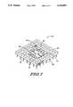
- FIG. 7is a perspective of a pin grid array (PGA) semiconductor device also in accordance with the present invention.
- PGApin grid array
- a semiconductor deviceincludes only external contacts which are needed by the device user during device operation, but allows the device manufacturer complete electrical access to the device for test purposes.
- contacts which are used for test purposes by device manufacturersare removed from the device prior to shipment to customers.
- Another form of the inventionestablishes test contacts which are configured differently than external contacts that are used during device operation, and in turn occupy less area. Using either form of the invention, or a combination of both forms, permits the size of a semiconductor device to be significantly reduced since external test contacts having the same configuration as external operational contacts are eliminated.
- test contactsWhile external operational contacts are constrained to standard positions and configurations, test contacts implemented in accordance with the present invention have no such constraints. Placement, size, and configuration of test contacts that are not need during device operation is left to the discretion of the semiconductor manufacturer. The flexibility of test contact placement and configuration results in a smaller device size. Moreover, the size advantage is achieved without an increase in device cost and without an increase in mounting complexity for the device user.
- over-molded pad array carriersOMPAC
- PGApin grid array
- DIPceramic dual inline plastic
- FIG. 1illustrates a top view of an OMPAC semiconductor device 10 in accordance with the present invention.
- Device 10includes a package substrate material 12, which is illustrated as a portion of a strip of material.
- package substrate 12is a bismaleimide-triazine resin (also know as BT resin) which is formed into a thin, flexible stripe or tape.
- the BT resinmay be formed as a composite material having glass fibers throughout.
- package substrate 12may be a thin, epoxy-glass composite material, similar to the materials used for printed circuit boards.
- the package substrate materialis in strip form to facilitate automated manufacturing of multiple semiconductor devices, although use of a package substrate material in strip form is not required in practicing the invention.
- package substrate 12has strip alignment holes 14 which are used to accurately index the strip through manufacturing equipment.
- Device alignment holes 15are provided in the package substrate and are used to align device 10 to manufacturing equipment once the device has been singulated or excised from the strip. Both the strip alignment holes and device alignment holes extend completely through the package substrate from a top surface to a bottom surface.
- each conductive traceelectrically couples a terminal or bond pad 18 of a semiconductor die 20 to an electrically conductive via 22.
- FIG. 3illustrates a cross-sectional view of device 10 taken along the line 3--3 of FIG. 1.
- the conductive tracesare electrically coupled to the die by conductive wires 23 which are similar to wires used in conventional semiconductor devices. As alternatives to using conductive wires, tape automated bonding (TAB), flip-chip techniques, and the like, may be used to electrically couple the die to the conductive traces.
- TABtape automated bonding
- Conductive traces 16are preferably copper or a plated copper material, such as gold-plated or nickel-plated copper, although other electrically conductive materials are suitable for use in the invention.
- Vias 22extend from the top surface of the package substrate to the bottom surface, and are typically plated with a conductive material along via sidewalls. Alternatively, vias may be filled with an electrically conductive material to provide electrical continuity through each via.
- the traces and viasare formed on package substrate 12 using conventional methods, for instance screen printing, plating, lithography, and etching techniques.
- device 10also includes a package body 24 which encapsulates semiconductor die 20, wire bonds 23, portions of conductive traces 16, and portions of the top surface of package substrate 12. Vias 22 may or may not be encapsulated by package body 24, depending on the location of vias in the package substrate.
- package body 24is formed of a molded plastic or epoxy resin which can be formed over die 20 using conventional one-sided molding equipment and materials.
- any encapsulant which provides adequate environmental protection to the dieis suitable for use in the present invention, including pre-formed plastic or ceramic package bodies or dispensed plastics known as glob top packages.
- each conductive trace formed on the top of package substrate 12is routed to a solder ball 26 on the bottom of the package substrate by conductive vias 22.
- the bottom of device 10, including package substrate 12 and solder balls 26,is illustrated in FIG. 2.
- Some viasare directly coupled to solder balls while other vias are routed to solder balls by conductive traces formed on the bottom of the package substrate.
- Solder balls which are directly coupled to viasare preferably filled vias to avoid substantial solder wicking into the via.
- Solder balls 26are attached to device 10 by providing a conductive solder pad (not illustrated because the pads are hidden by the solder balls) on the package substrate at the end of a conductive trace or surrounding a conductive via.
- solder padsare formed on the package substrate by conventional techniques, usually at the same time conductive traces 16 are formed, and are of a material which is readily bonded to solder, such as a nickel-plated or gold-plated material.
- solder balls of device 10are external contacts which are used to electrically access semiconductor die 20.
- device 10is mounted to a user substrate (not illustrated), such as a printed circuit board.
- solder balls 26correspond in position to conductive pads or terminals formed on the user substrate. The solder balls are reflowed and bonded to the pads, thereby affixing the device to the user substrate.
- the external contacts of a semiconductor devicemay not be necessary in a user application, but are used only for a manufacturer's internal testing. These unnecessary external contacts undesirably increase the overall size of a semiconductor device.
- the external contactsin this case solder balls 26, take up a substantial portion of the overall device size or area. Although positioning the solder balls closer together would reduce size of the device, there is a lower limit to the solder ball spacing or pitch for a given solder ball diameter from a manufacturing point of view. As solder balls are placed closer together, it is more difficult for a user to mount the device to a substrate, such as a printed circuit board.
- the size of a semiconductor deviceis reduced by removing the external test contacts not needed by the user or by configuring the test contacts in a way which does not require additional space.
- device 10includes two boundaries, boundary A and boundary B.
- Boundary Adefines the size of device 10 as the device is provided to a user. Within boundary A are all external contacts (solder balls) and all electrical connections to semiconductor die 20 which are necessary for user-defined device operation (some device users may require more contacts than others).
- Boundary Bdefines the size of device 10 required to include all external contacts necessary for device operation and for the manufacturer's internal testing.
- boundary A and Ba difference between boundaries A and B is that the external contacts needed only for testing purposes (hereinafter referred to as test-only contacts) are contained within boundary B, but are excluded from boundary A.
- the test-only contactsare positioned peripherally around the device.
- the solder balls positioned between boundary A and boundary Bare used for the manufacturer's testing purposes and the solder balls positioned within boundary A are used for device operation in a user application. It is important to also point out that the solder balls or contacts within boundary A may also be used during device testing. However, the solder balls between boundaries A and B, the test-only contacts, cannot be needed for user-defined device operation.
- the portion of package substrate 12 to which the test-only solder balls are attachedcan be removed after testing, thereby reducing the size of the device provided to a user.
- the size reduction achieved as a result of removing portions of the package substrateis apparent in viewing FIG. 3.
- the deviceis ready for testing. Testing can be accomplished either in strip form, or each device of the package substrate strip can be singulated and individually tested. If singulating the devices prior to testing, package substrate 12 is cut using conventional methods along boundary B. In reference to the cross-sectional view of FIG. 3, there are seven solder balls attached to the illustrated portion of device 10 after singulating the device from the package substrate strip along boundary B.
- Device 10is then tested in a known manner.
- semiconductor die 20is electrically accessed by the solder balls present on the bottom of package substrate 12.
- the test-only solder balls located around the device peripheryare removed by cutting the package substrate along boundary A.
- two solder ballsare removed upon cutting substrate 12 along boundary A.
- a total of eighteen solder ballsare removed upon cutting along boundary A.
- the size of device 10 that is sent to a useris considerably smaller than if the device included the test-only solder balls as in conventional devices. If singulating the devices after testing, only one excising operation is necessary.
- the devicesare tested in strip form and the package substrate is then cut along boundary A.
- a conventional 144-pin OMPAC devicehaving solder balls arranged in twelve rows and twelve columns has an area on the order of 264 mm 2 (16.25 mm ⁇ 16.25 mm). Assume that forty-four of the pins of the conventional device are not needed by the user, but are necessary for manufacturer's testing purposes.
- a 100-pin OMPAChaving an area on the order of 176 mm 2 (13.25 mm ⁇ 13.25 mm) could be used in place of the 264 mm 2 144-pin OMPAC without sacrificing functionality.
- a possible disadvantage of removing the test-only contacts of a semiconductor deviceis that electrical access to certain portions of a semiconductor die becomes extremely difficult, if not impossible. Not having full access to the die can create problems for users and manufacturers when it comes to debugging or performing failure analysis on the device.
- One methodis to configure the conductive traces and conductive vias associated with the test-only contacts to permit electrical access to portions of the die even after the test-only contacts have been removed.
- FIG. 3illustrates that boundary A cuts through one of the conductive vias. From FIG. 2 it is apparent that boundary A cuts through several vias.
- castellations 28are formed along the periphery of the package substrate, as illustrated in a perspective view of device 10 in FIG. 4. Because vias 22 are electrically conductive the whole way through the package substrate, castellations 28 are also electrically conductive. Therefore, access to the test portions of semiconductor die 20 can be achieved through the conductive castellations. Test probes can be abutted to the conductive castellations to perform certain testing operations after the external test-only solder balls have been removed. Notice that not all vias associated with test-only solder balls are formed into castellations, but that some vias are completely removed from the device upon cutting along boundary A. A device manufacturer may provide the more useful or significant test contacts with castellations, while providing no electrical access to others.
- conductive traces 16may be covered completely, or in part, by a solder resist or a solder mask (not illustrated). Solder resist materials are well known in semiconductor manufacturing and are used to mask or protect appropriate areas from subsequent solder applications. Thus, conductive traces on the top of a package substrate may not be available for electrical contact if covered by solder resist. Castellations 28, on the other hand, have exposed conductive regions along the periphery of package substrate 12 which are suitable for contacting and would not be covered by solder resist.
- FIGS. 5 and 6which are respectively top and bottom views of a semiconductor device 30, illustrate two such methods.
- Device 30is similar to device 10 of FIGS. 1-4, and includes many of the same elements. Analogous elements of the two devices have the same reference labels.
- device 30, unlike device 10includes a plurality of test pads 32 formed on top of package substrate 12. The test pads can be formed on the package substrate at the same time conductive traces 16 are formed, and may be of a similar or the same material. Although the test pads are illustrated as being square, any test pad shape may be used in accordance with the present invention.
- test pads 32formed at the ends of selected conductive traces 16, or along any portion of a conductive trace, will provide appropriate electrical continuity.
- the conductive traces having test pads 32are routed under package body 24 and are electrically coupled to bond pads of a semiconductor die (not shown) which are used for device testing, but which are not needed for user-defined device operation.
- test pads 32enable certain electrical testing to be performed on device 30, even though test-only external contacts, such as solder balls, have be excised from the device. Because contact to the test pads is not necessary for device operation, the test pads do not have to be coupled to external contacts and device size can be minimized.
- test padscan be included in a semiconductor device to permit testing of the device after external test-only contact have been removed.
- test padscan be provided in place of test-only external contacts. Rather than routing a conductive trace to a peripheral test-only solder ball and excising the solder ball after device testing, the device may be tested using test pads.
- the conductive traces designated for test-only purposesmay include test pads 32 or castellations 28. These conductive traces are not routed to solder balls or any type of external contact on the bottom of the package substrate. Only those conductive traces which are used during device operation are routed to solder balls or other external contacts.
- test pads 32are provided on the top surface of package substrate 12 whereas solder balls are attached to the bottom surface.
- testing equipmentwhich provides both top-side and bottom-side contact is not required to test a device formed in accordance with the present invention because test pads 32 may be formed on the bottom of package substrate 12 as well.
- a bottom view of device 30is illustrated in FIG. 6 and includes bottom-side test pads 32.
- Pogo-pinsare spring loaded pins that have adjustable positions. The spring forces the pin outward until the pins meets an opposing surface, namely a contact. For example, in testing device 30 of FIG. 6 using a plurality of pogo-pins, the pogo-pins aligned to the solder balls would extend outward until contacting the solder balls, whereas the pogo-pins aligned to the test pads would extend further to contact the test pads.
- test pads 32are several advantages to using test pads 32, either alone or in combination with peripheral test-only contacts which are removed from the device.
- One advantageis that spacing limitations of test pads are more relaxed than those of solder balls.
- Test padsare lithographically defined on the package substrate, and therefore can be made quite small.
- the only size limitation to the test padsis that a test probe, such as a pogo-pin, be able to reliably contact the pad. Because the test pads can be made small and placed closed together, numerous test pads can be placed among solder balls on the bottom of a package substrate and also among conductive traces on the top of the package substrate. As a result, size of a semiconductor device in accordance with the present invention is reduced in comparison to conventional devices which have external pins or contacts that are not used during device operation.
- test padsUsed alone, test pads have the advantage of utilizing a smaller package substrate area than if external test-only contacts are included. Furthermore, the need to cut portions of the package substrate which have external test-only contacts is eliminated, which may result in fewer manufacturing steps.
- the use of test pads in conjunction with external test-only contacts which are excised before shipment to a customeralso has an advantage. Manufacturer's testing can be accomplished using solely external contacts of a device. However, supplemental test pads enable electrical accessibility to certain portions of a semiconductor die which are otherwise lost upon excising external test-only contacts from the device. Using supplemental test pads in conjunction with external contacts which are designated as test-only contacts permits debugging and failure analysis to be performed on the device even though the original test-only contacts are removed.
- FIG. 7a pin grid array (PGA) semiconductor device 50 in accordance with the present invention.
- Device 50includes a package substrate 52, which as in many conventional PGA devices is a pre-formed, multilayer ceramic package.
- Package substrate 52includes a cavity 54 for housing a semiconductor die 56. Attached to a bottom surface of package substrate 52 is a plurality of external operational contacts or pins 58.
- the operational pinsare electrically routed to a plurality of conductive traces 60 formed on a surface of the package substrate within cavity 54. Electrical routing is achieved through various conductive layers and conductive vias (not shown) throughout package substrate 54, as is well known in the art.
- the operational pinsare electrically coupled to portions of semiconductor die 56 used during device operation by the conductive traces and by wire bonds 62 which are bonded to bond pads 64 of the die.
- conductive tracesfor purposes of clarity, not all conductive traces, bond pads, or wire bonds that would normally be associated with device 50 are illustrated. Nonetheless, one skilled in the art will clearly understand the essential aspects of the invention.
- package substrate 52also includes a plurality of test contacts or pads 66 formed on a top surface of the substrate.
- the test padsmay instead be formed on a bottom surface of the substrate or on a combination of both the top and bottom surfaces.
- Test pads 66are formed on the package substrate using conventional techniques, such as plating, screen printing, or the like.
- test pads 66are electrically coupled to portions of semiconductor die 56 which are used during device testing, and not during user-defined device operation.
- the test padsare also coupled to the die by conductive vias (not shown), conductive traces, wire bonds, and bonding pads, as are external operational pins 58.
- test padsare coupled to a first set of bond pads which access test portions of the die, whereas the operational pins are coupled to a second set of bond pads which access operational portions of the die.
- the test portions of the diecannot readily be accessed during normal device operation.
- the test portion of the diewhich includes the bond pads associated with the test pads
- the operational portion of the diewhich includes the bond pads associated with the external operational pins.
- Utilizing test pads 66eliminates the need to bring all conductive traces and bond pads out of the package substrate in the form of external pins. Consequently, device 50 can be made smaller than conventional PGA devices.
- test pads in accordance with the present inventionmay be formed on a top surface, a bottom surface, or along a periphery of a package substrate. Also, it is not required that each conductive trace having a corresponding conductive via or a corresponding test pad. Conductive traces may either be used for test-only purposes or for user-operation purposes. Those traces for user-operation will have a corresponding external contact, whereas the traces used for test-only purposes will not have a corresponding external contact of the same configuration as the external operational contact, in accordance with the present invention, upon completion of device manufacturing. It is also important to note that the present invention is applicable packaging techniques other than OMPAC, such as multichip modules, PGAs, ceramic DIPs, and the like. Therefore, it is intended that this invention encompass all such variations and modifications as fall within the scope of the appended claims.
Landscapes
- Engineering & Computer Science (AREA)
- Microelectronics & Electronic Packaging (AREA)
- Physics & Mathematics (AREA)
- Computer Hardware Design (AREA)
- General Physics & Mathematics (AREA)
- Power Engineering (AREA)
- Condensed Matter Physics & Semiconductors (AREA)
- Manufacturing & Machinery (AREA)
- General Engineering & Computer Science (AREA)
- Geometry (AREA)
- Testing Or Measuring Of Semiconductors Or The Like (AREA)
- Testing Of Individual Semiconductor Devices (AREA)
Abstract
Description
Claims (22)
Priority Applications (4)
| Application Number | Priority Date | Filing Date | Title |
|---|---|---|---|
| US07/864,246US5334857A (en) | 1992-04-06 | 1992-04-06 | Semiconductor device with test-only contacts and method for making the same |
| EP93104432AEP0564865A1 (en) | 1992-04-06 | 1993-03-18 | Semiconductor device with test-only contacts and method for making the same |
| JP5090492AJPH0621173A (en) | 1992-04-06 | 1993-03-26 | Manufacture of semiconductor device provided with contact for test use only |
| KR1019930005518AKR930022510A (en) | 1992-04-06 | 1993-03-31 | Method of manufacturing a semiconductor device having only test contacts |
Applications Claiming Priority (1)
| Application Number | Priority Date | Filing Date | Title |
|---|---|---|---|
| US07/864,246US5334857A (en) | 1992-04-06 | 1992-04-06 | Semiconductor device with test-only contacts and method for making the same |
Publications (1)
| Publication Number | Publication Date |
|---|---|
| US5334857Atrue US5334857A (en) | 1994-08-02 |
Family
ID=25342828
Family Applications (1)
| Application Number | Title | Priority Date | Filing Date |
|---|---|---|---|
| US07/864,246Expired - LifetimeUS5334857A (en) | 1992-04-06 | 1992-04-06 | Semiconductor device with test-only contacts and method for making the same |
Country Status (4)
| Country | Link |
|---|---|
| US (1) | US5334857A (en) |
| EP (1) | EP0564865A1 (en) |
| JP (1) | JPH0621173A (en) |
| KR (1) | KR930022510A (en) |
Cited By (94)
| Publication number | Priority date | Publication date | Assignee | Title |
|---|---|---|---|---|
| US5578869A (en)* | 1994-03-29 | 1996-11-26 | Olin Corporation | Components for housing an integrated circuit device |
| US5598036A (en)* | 1995-06-15 | 1997-01-28 | Industrial Technology Research Institute | Ball grid array having reduced mechanical stress |
| WO1997012400A1 (en)* | 1995-09-29 | 1997-04-03 | Intel Corporation | An integrated circuit package with permanent identification of device characteristics and method for adding the same |
| WO1997024763A1 (en)* | 1995-12-29 | 1997-07-10 | Intel Corporation | An integrated circuit package with internally readable permanent identification of device characteristics |
| US5650595A (en)* | 1995-05-25 | 1997-07-22 | International Business Machines Corporation | Electronic module with multiple solder dams in soldermask window |
| US5717252A (en)* | 1994-07-25 | 1998-02-10 | Mitsui High-Tec, Inc. | Solder-ball connected semiconductor device with a recessed chip mounting area |
| US5719449A (en)* | 1996-09-30 | 1998-02-17 | Lucent Technologies Inc. | Flip-chip integrated circuit with improved testability |
| US5723901A (en)* | 1994-12-13 | 1998-03-03 | Kabushiki Kaisha Toshiba | Stacked semiconductor device having peripheral through holes |
| US5726493A (en)* | 1994-06-13 | 1998-03-10 | Fujitsu Limited | Semiconductor device and semiconductor device unit having ball-grid-array type package structure |
| US5729051A (en)* | 1994-09-22 | 1998-03-17 | Nec Corporation | Tape automated bonding type semiconductor device |
| US5728600A (en)* | 1994-11-15 | 1998-03-17 | Vlt Corporation | Circuit encapsulation process |
| US5729894A (en)* | 1992-07-21 | 1998-03-24 | Lsi Logic Corporation | Method of assembling ball bump grid array semiconductor packages |
| US5731709A (en)* | 1996-01-26 | 1998-03-24 | Motorola, Inc. | Method for testing a ball grid array semiconductor device and a device for such testing |
| US5760643A (en)* | 1995-10-31 | 1998-06-02 | Texas Instruments Incorporated | Integrated circuit die with selective pad-to-pad bypass of internal circuitry |
| US5763947A (en)* | 1996-01-31 | 1998-06-09 | International Business Machines Corporation | Integrated circuit chip package having configurable contacts and a removable connector |
| US5767528A (en)* | 1996-02-20 | 1998-06-16 | Fujitsu Limited | Semiconductor device including pad portion for testing |
| WO1998048458A1 (en)* | 1997-04-21 | 1998-10-29 | Lsi Logic Corporation | Ball grid array package employing solid core solder balls |
| US5844315A (en)* | 1996-03-26 | 1998-12-01 | Motorola Corporation | Low-profile microelectronic package |
| US5854512A (en)* | 1996-09-20 | 1998-12-29 | Vlsi Technology, Inc. | High density leaded ball-grid array package |
| US5866941A (en)* | 1995-02-23 | 1999-02-02 | Silicon Systems, Inc. | Ultra thin, leadless and molded surface mount integrated circuit package |
| US5869869A (en)* | 1996-01-31 | 1999-02-09 | Lsi Logic Corporation | Microelectronic device with thin film electrostatic discharge protection structure |
| US5869886A (en)* | 1996-03-22 | 1999-02-09 | Nec Corporation | Flip chip semiconductor mounting structure with electrically conductive resin |
| US5909054A (en)* | 1995-05-16 | 1999-06-01 | Kabushiki Kaisha Toshiba | Semiconductor device having a multiple-terminal integrated circuit formed on a circuit substrate |
| US5945130A (en)* | 1994-11-15 | 1999-08-31 | Vlt Corporation | Apparatus for circuit encapsulation |
| US5969538A (en)* | 1996-10-31 | 1999-10-19 | Texas Instruments Incorporated | Semiconductor wafer with interconnect between dies for testing and a process of testing |
| US5994912A (en)* | 1995-10-31 | 1999-11-30 | Texas Instruments Incorporated | Fault tolerant selection of die on wafer |
| US5998861A (en)* | 1995-09-28 | 1999-12-07 | Kabushiki Kaisha Toshiba | Semiconductor device having ball grid array |
| US6020629A (en)* | 1998-06-05 | 2000-02-01 | Micron Technology, Inc. | Stacked semiconductor package and method of fabrication |
| US6034426A (en)* | 1997-10-30 | 2000-03-07 | Hewlett-Packard Co. | Testable low inductance integrated circuit package |
| US6046600A (en)* | 1995-10-31 | 2000-04-04 | Texas Instruments Incorporated | Process of testing integrated circuit dies on a wafer |
| US6048753A (en)* | 1996-04-02 | 2000-04-11 | Micron Technology, Inc. | Standardized bonding location process and apparatus |
| US6093958A (en)* | 1998-01-19 | 2000-07-25 | Nec Corporation | Lead-on-chip type semiconductor device having thin plate and method for manufacturing the same |
| US6098283A (en)* | 1996-12-19 | 2000-08-08 | Intel Corporation | Method for filling vias in organic, multi-layer packages |
| US6107679A (en)* | 1997-12-22 | 2000-08-22 | Oki Electric Industry Co., Ltd. | Semiconductor device |
| US6125042A (en)* | 1998-04-10 | 2000-09-26 | Lucent Technologies, Inc. | Ball grid array semiconductor package having improved EMI characteristics |
| US6128201A (en)* | 1997-05-23 | 2000-10-03 | Alpine Microsystems, Inc. | Three dimensional mounting assembly for integrated circuits |
| US6175161B1 (en) | 1998-05-22 | 2001-01-16 | Alpine Microsystems, Inc. | System and method for packaging integrated circuits |
| US6194250B1 (en) | 1998-09-14 | 2001-02-27 | Motorola, Inc. | Low-profile microelectronic package |
| US6221682B1 (en) | 1999-05-28 | 2001-04-24 | Lockheed Martin Corporation | Method and apparatus for evaluating a known good die using both wire bond and flip-chip interconnects |
| US6239496B1 (en)* | 1999-01-18 | 2001-05-29 | Kabushiki Kaisha Toshiba | Package having very thin semiconductor chip, multichip module assembled by the package, and method for manufacturing the same |
| US6247629B1 (en)* | 1997-09-08 | 2001-06-19 | Micron Technology, Inc. | Wire bond monitoring system for layered packages |
| US20010047882A1 (en)* | 1997-12-19 | 2001-12-06 | William A. Samaras | Multi-chip land grid array carrier |
| US20020053452A1 (en)* | 1996-09-04 | 2002-05-09 | Quan Son Ky | Semiconductor package and method therefor |
| US6400170B1 (en)* | 1998-08-26 | 2002-06-04 | Yazaki Corporation | High current examining structure for a circuit protective element |
| US6420789B1 (en)* | 2000-05-16 | 2002-07-16 | Micron Technology, Inc. | Ball grid array chip packages having improved testing and stacking characteristics |
| US6451624B1 (en) | 1998-06-05 | 2002-09-17 | Micron Technology, Inc. | Stackable semiconductor package having conductive layer and insulating layers and method of fabrication |
| US6459161B1 (en)* | 1998-11-10 | 2002-10-01 | Nec Corporation | Semiconductor device with connection terminals in the form of a grid array |
| US6469530B1 (en) | 2000-02-15 | 2002-10-22 | Agilent Technologies, Inc. | Method and apparatus for testing of ball grid array circuitry |
| US20020195695A1 (en)* | 2001-05-30 | 2002-12-26 | Miyoshi Togawa | Substrate for semiconductor device, manufacturing method thereof, semiconductor device, and frame main body |
| US6507117B1 (en)* | 1999-01-29 | 2003-01-14 | Rohm Co., Ltd. | Semiconductor chip and multichip-type semiconductor device |
| US6582992B2 (en) | 2001-11-16 | 2003-06-24 | Micron Technology, Inc. | Stackable semiconductor package and wafer level fabrication method |
| US20030137030A1 (en)* | 2002-01-22 | 2003-07-24 | Lunde Aron T. | Die assembly and method for forming a die on a wafer |
| US20030143781A1 (en)* | 2002-01-31 | 2003-07-31 | Mclellan Neil Robert | Encapsulated integrated circuit package and method of manufacturing an integrated circuit package |
| US6610591B1 (en) | 2000-08-25 | 2003-08-26 | Micron Technology, Inc. | Methods of ball grid array |
| US20030159282A1 (en)* | 2002-02-26 | 2003-08-28 | Seiko Epson Corporation | Wiring board and method of fabricating the same, semiconductor device, and electronic instrument |
| US20030215966A1 (en)* | 2002-05-14 | 2003-11-20 | Rolda Ruben A. | Circular test pads on scribe street area |
| US20030234454A1 (en)* | 2002-06-24 | 2003-12-25 | Serafin Pedron | Integrated circuit package and method of manufacturing the integrated circuit package |
| US6675472B1 (en) | 1999-04-29 | 2004-01-13 | Unicap Electronics Industrial Corporation | Process and structure for manufacturing plastic chip carrier |
| US6683468B1 (en)* | 2001-08-29 | 2004-01-27 | Cypress Semiconductor Corporation | Method and apparatus for coupling to a device packaged using a ball grid array |
| US20040033673A1 (en)* | 2002-08-15 | 2004-02-19 | Cobbley Chad A. | Method of packaging semiconductor dice employing at least one redistribution layer |
| US20040046241A1 (en)* | 2002-03-22 | 2004-03-11 | Combs Edward G. | Method of manufacturing enhanced thermal dissipation integrated circuit package |
| US6711812B1 (en) | 1999-04-13 | 2004-03-30 | Unicap Electronics Industrial Corporation | Method of making metal core substrate printed circuit wiring board enabling thermally enhanced ball grid array (BGA) packages |
| US6728915B2 (en) | 2000-01-10 | 2004-04-27 | Texas Instruments Incorporated | IC with shared scan cells selectively connected in scan path |
| US6734552B2 (en) | 2001-07-11 | 2004-05-11 | Asat Limited | Enhanced thermal dissipation integrated circuit package |
| US6763485B2 (en) | 1998-02-25 | 2004-07-13 | Texas Instruments Incorporated | Position independent testing of circuits |
| US6769080B2 (en) | 2000-03-09 | 2004-07-27 | Texas Instruments Incorporated | Scan circuit low power adapter with counter |
| US20040245628A1 (en)* | 2003-01-14 | 2004-12-09 | Samsung Electronics Co., Ltd. | Tape package having test pad on reverse surface and method for testing the same |
| US20050082667A1 (en)* | 2003-09-18 | 2005-04-21 | Gavin Gibson | Rewiring substrate strip with a number of semiconductor component positions |
| US6975980B2 (en) | 1998-02-18 | 2005-12-13 | Texas Instruments Incorporated | Hierarchical linking module connection to access ports of embedded cores |
| US20060043569A1 (en)* | 2004-08-27 | 2006-03-02 | Benson Peter A | Low temperature methods of forming back side redistribution layers in association with through wafer interconnects, semiconductor devices including same, and assemblies |
| US7015072B2 (en) | 2001-07-11 | 2006-03-21 | Asat Limited | Method of manufacturing an enhanced thermal dissipation integrated circuit package |
| US7058862B2 (en) | 2000-05-26 | 2006-06-06 | Texas Instruments Incorporated | Selecting different 1149.1 TAP domains from update-IR state |
| US20060163573A1 (en)* | 2001-05-21 | 2006-07-27 | Hall Frank L | Method for preparing ball grid array substrates via use of a laser |
| US20060286689A1 (en)* | 2005-06-17 | 2006-12-21 | Matsushita Electric Industrial Co., Ltd. | Semiconductor device and manufacturing method thereof |
| US20070152215A1 (en)* | 2005-12-29 | 2007-07-05 | Hem Takiar | Test pads on flash memory cards |
| US20070283191A1 (en)* | 2003-12-19 | 2007-12-06 | Mcdonald-Maier Klaus D | Integrated Circuit with Debug Support Interface |
| US20080042252A1 (en)* | 1998-06-30 | 2008-02-21 | Micron Technology, Inc. | Stackable ceramic fbga for high thermal applications |
| US20080054261A1 (en)* | 2006-09-06 | 2008-03-06 | Samsung Electronics Co., Ltd. | Semiconductor package having test pads on top and bottom substrate surfaces and method of testing same |
| US20080289867A1 (en)* | 1994-12-05 | 2008-11-27 | Freescale Semiconductor, Inc. | Multi-strand substrate for ball-grid array assemblies and method |
| US20090127699A1 (en)* | 2007-11-15 | 2009-05-21 | Shin Hyun-Ok | Low temperature co-fired ceramics substrate and semiconductor package |
| US20090147490A1 (en)* | 2007-12-10 | 2009-06-11 | Panasonic Corporation | Substrate for wiring, semiconductor device for stacking using the same, and stacked semiconductor module |
| US20090267171A1 (en)* | 2008-04-24 | 2009-10-29 | Micron Technology, Inc. | Pre-encapsulated cavity interposer |
| US20090283888A1 (en)* | 2008-05-16 | 2009-11-19 | A Leam Choi | Package system incorporating a flip-chip assembly |
| US7714426B1 (en)* | 2007-07-07 | 2010-05-11 | Keith Gann | Ball grid array package format layers and structure |
| US8022521B1 (en)* | 2008-11-12 | 2011-09-20 | Amkor Technology, Inc. | Package failure prognostic structure and method |
| US20120319288A1 (en)* | 2011-06-17 | 2012-12-20 | Biotronik Se & Co. Kg | Semiconductor Package |
| US20130175528A1 (en)* | 2012-01-09 | 2013-07-11 | Samsung Electronics Co., Ltd. | Chip on film package including test pads and semiconductor devices including the same |
| US20130312123A1 (en)* | 2012-05-17 | 2013-11-21 | Silicon Motion, Inc. | Embedded multimediacard and electronic device using the same, and energining board for embedded multimediacard |
| US9134366B2 (en) | 2013-08-27 | 2015-09-15 | Freescale Semiconductor, Inc. | Method for forming a packaged semiconductor device |
| US9241407B2 (en) | 2012-01-25 | 2016-01-19 | Samsung Electronics Co., Ltd. | Tape film packages and methods of fabricating the same |
| CN106847719A (en)* | 2016-11-28 | 2017-06-13 | 西安科锐盛创新科技有限公司 | It is applied to the naked core chip architecture and its manufacture method of test |
| CN106856177A (en)* | 2016-11-28 | 2017-06-16 | 西安科锐盛创新科技有限公司 | It is applied to the naked core chip architecture and its manufacture method of test |
| US20200006163A1 (en)* | 2018-06-28 | 2020-01-02 | Western Digital Technologies, Inc. | Semiconductor device including through-package debug features |
| US20230207401A1 (en)* | 2021-12-23 | 2023-06-29 | Micron Technology, Inc. | Analog sense points for measuring circuit die |
Families Citing this family (18)
| Publication number | Priority date | Publication date | Assignee | Title |
|---|---|---|---|---|
| US5367763A (en)* | 1993-09-30 | 1994-11-29 | Atmel Corporation | TAB testing of area array interconnected chips |
| US6111306A (en) | 1993-12-06 | 2000-08-29 | Fujitsu Limited | Semiconductor device and method of producing the same and semiconductor device unit and method of producing the same |
| US5679978A (en)* | 1993-12-06 | 1997-10-21 | Fujitsu Limited | Semiconductor device having resin gate hole through substrate for resin encapsulation |
| JP2569400B2 (en)* | 1994-06-23 | 1997-01-08 | 九州日本電気株式会社 | Method for manufacturing resin-encapsulated semiconductor device |
| JPH0883866A (en)* | 1994-07-15 | 1996-03-26 | Shinko Electric Ind Co Ltd | Production of single side resin sealed semiconductor device and carrier frame therefor |
| EP0767492A3 (en)* | 1995-10-02 | 1998-09-09 | Altera Corporation | Integrated circuit test system |
| FR2742548B1 (en)* | 1995-12-19 | 1998-01-16 | Siemens Automotive Sa | ELECTRONIC MODULE |
| US5859538A (en)* | 1996-01-31 | 1999-01-12 | Hewlett-Packard Company | Method and apparatus for connecting a ball grid array device to a test instrument to facilitate the monitoring of individual signals or the interruption of individual signals or both |
| US6020758A (en)* | 1996-03-11 | 2000-02-01 | Altera Corporation | Partially reconfigurable programmable logic device |
| JPH10284535A (en)* | 1997-04-11 | 1998-10-23 | Toshiba Corp | Semiconductor device manufacturing method and semiconductor component |
| KR100258350B1 (en)* | 1997-05-13 | 2000-06-01 | 마이클 디. 오브라이언 | Super bga semiconductor package |
| DE19831634B4 (en) | 1998-07-15 | 2005-02-03 | Pac Tech - Packaging Technologies Gmbh | Chip carrier arrangement and method for producing a chip carrier arrangement with an electrical test |
| WO2000019532A1 (en)* | 1998-09-30 | 2000-04-06 | Conexant Systems, Inc. | Package for providing improved electrical contact and methods for forming the same |
| WO2000044041A1 (en) | 1999-01-22 | 2000-07-27 | Hitachi, Ltd. | Semiconductor integrated circuit and manufacture thereof |
| JP2001313127A (en) | 2000-04-28 | 2001-11-09 | Nec Corp | Electrostatic breakdown preventing device in electronic equipment |
| JP4583850B2 (en)* | 2004-09-16 | 2010-11-17 | 富士通セミコンダクター株式会社 | Semiconductor device and manufacturing method thereof |
| US9153507B2 (en)* | 2012-01-31 | 2015-10-06 | Broadcom Corporation | Semiconductor package with improved testability |
| US20180315672A1 (en)* | 2017-04-26 | 2018-11-01 | Qualcomm Incorporated | Sacrificial test pads for inline test access |
Citations (6)
| Publication number | Priority date | Publication date | Assignee | Title |
|---|---|---|---|---|
| US4437141A (en)* | 1981-09-14 | 1984-03-13 | Texas Instruments Incorporated | High terminal count integrated circuit device package |
| JPS5963751A (en)* | 1982-10-04 | 1984-04-11 | Matsushita Electronics Corp | Semiconductor device |
| US4881029A (en)* | 1985-09-30 | 1989-11-14 | Kabushiki Kaisha Toshiba | Semiconductor integrated circuit devices and methods for testing same |
| JPH02211648A (en)* | 1989-02-11 | 1990-08-22 | Nec Ic Microcomput Syst Ltd | Semiconductor device |
| US4975765A (en)* | 1988-07-22 | 1990-12-04 | Contraves Ag | Highly integrated circuit and method for the production thereof |
| US5065227A (en)* | 1990-06-04 | 1991-11-12 | International Business Machines Corporation | Integrated circuit packaging using flexible substrate |
Family Cites Families (2)
| Publication number | Priority date | Publication date | Assignee | Title |
|---|---|---|---|---|
| US4970454A (en)* | 1986-12-09 | 1990-11-13 | Texas Instruments Incorporated | Packaged semiconductor device with test circuits for determining fabrication parameters |
| US5018005A (en)* | 1989-12-27 | 1991-05-21 | Motorola Inc. | Thin, molded, surface mount electronic device |
- 1992
- 1992-04-06USUS07/864,246patent/US5334857A/ennot_activeExpired - Lifetime
- 1993
- 1993-03-18EPEP93104432Apatent/EP0564865A1/ennot_activeWithdrawn
- 1993-03-26JPJP5090492Apatent/JPH0621173A/enactivePending
- 1993-03-31KRKR1019930005518Apatent/KR930022510A/ennot_activeAbandoned
Patent Citations (6)
| Publication number | Priority date | Publication date | Assignee | Title |
|---|---|---|---|---|
| US4437141A (en)* | 1981-09-14 | 1984-03-13 | Texas Instruments Incorporated | High terminal count integrated circuit device package |
| JPS5963751A (en)* | 1982-10-04 | 1984-04-11 | Matsushita Electronics Corp | Semiconductor device |
| US4881029A (en)* | 1985-09-30 | 1989-11-14 | Kabushiki Kaisha Toshiba | Semiconductor integrated circuit devices and methods for testing same |
| US4975765A (en)* | 1988-07-22 | 1990-12-04 | Contraves Ag | Highly integrated circuit and method for the production thereof |
| JPH02211648A (en)* | 1989-02-11 | 1990-08-22 | Nec Ic Microcomput Syst Ltd | Semiconductor device |
| US5065227A (en)* | 1990-06-04 | 1991-11-12 | International Business Machines Corporation | Integrated circuit packaging using flexible substrate |
Non-Patent Citations (1)
| Title |
|---|
| Semiconductor Wafer Testing, D. E. Shultis, Dec. 1970, IBM Technical Disclosure Bulletin vol. 13 No. 7 p. 1793.* |
Cited By (176)
| Publication number | Priority date | Publication date | Assignee | Title |
|---|---|---|---|---|
| US5729894A (en)* | 1992-07-21 | 1998-03-24 | Lsi Logic Corporation | Method of assembling ball bump grid array semiconductor packages |
| US5578869A (en)* | 1994-03-29 | 1996-11-26 | Olin Corporation | Components for housing an integrated circuit device |
| US5726493A (en)* | 1994-06-13 | 1998-03-10 | Fujitsu Limited | Semiconductor device and semiconductor device unit having ball-grid-array type package structure |
| US5717252A (en)* | 1994-07-25 | 1998-02-10 | Mitsui High-Tec, Inc. | Solder-ball connected semiconductor device with a recessed chip mounting area |
| US5729051A (en)* | 1994-09-22 | 1998-03-17 | Nec Corporation | Tape automated bonding type semiconductor device |
| US6710257B2 (en) | 1994-11-15 | 2004-03-23 | Vlt Corporation | Circuit encapsulation |
| US6403009B1 (en) | 1994-11-15 | 2002-06-11 | Vlt Corporation | Circuit encapsulation |
| US5728600A (en)* | 1994-11-15 | 1998-03-17 | Vlt Corporation | Circuit encapsulation process |
| US5945130A (en)* | 1994-11-15 | 1999-08-31 | Vlt Corporation | Apparatus for circuit encapsulation |
| US20080289867A1 (en)* | 1994-12-05 | 2008-11-27 | Freescale Semiconductor, Inc. | Multi-strand substrate for ball-grid array assemblies and method |
| US5723901A (en)* | 1994-12-13 | 1998-03-03 | Kabushiki Kaisha Toshiba | Stacked semiconductor device having peripheral through holes |
| US5866941A (en)* | 1995-02-23 | 1999-02-02 | Silicon Systems, Inc. | Ultra thin, leadless and molded surface mount integrated circuit package |
| US5909054A (en)* | 1995-05-16 | 1999-06-01 | Kabushiki Kaisha Toshiba | Semiconductor device having a multiple-terminal integrated circuit formed on a circuit substrate |
| US5798285A (en)* | 1995-05-25 | 1998-08-25 | International Business Machines Corpoation | Method of making electronic module with multiple solder dams in soldermask window |
| US5650595A (en)* | 1995-05-25 | 1997-07-22 | International Business Machines Corporation | Electronic module with multiple solder dams in soldermask window |
| US5598036A (en)* | 1995-06-15 | 1997-01-28 | Industrial Technology Research Institute | Ball grid array having reduced mechanical stress |
| US5998861A (en)* | 1995-09-28 | 1999-12-07 | Kabushiki Kaisha Toshiba | Semiconductor device having ball grid array |
| US5686759A (en)* | 1995-09-29 | 1997-11-11 | Intel Corporation | Integrated circuit package with permanent identification of device characteristics and method for adding the same |
| US5670825A (en)* | 1995-09-29 | 1997-09-23 | Intel Corporation | Integrated circuit package with internally readable permanent identification of device characteristics |
| WO1997012400A1 (en)* | 1995-09-29 | 1997-04-03 | Intel Corporation | An integrated circuit package with permanent identification of device characteristics and method for adding the same |
| US6727722B2 (en) | 1995-10-31 | 2004-04-27 | Texas Instruments Incorporated | Process of testing a semiconductor wafer of IC dies |
| US5994912A (en)* | 1995-10-31 | 1999-11-30 | Texas Instruments Incorporated | Fault tolerant selection of die on wafer |
| US6046600A (en)* | 1995-10-31 | 2000-04-04 | Texas Instruments Incorporated | Process of testing integrated circuit dies on a wafer |
| US5760643A (en)* | 1995-10-31 | 1998-06-02 | Texas Instruments Incorporated | Integrated circuit die with selective pad-to-pad bypass of internal circuitry |
| WO1997024763A1 (en)* | 1995-12-29 | 1997-07-10 | Intel Corporation | An integrated circuit package with internally readable permanent identification of device characteristics |
| US5731709A (en)* | 1996-01-26 | 1998-03-24 | Motorola, Inc. | Method for testing a ball grid array semiconductor device and a device for such testing |
| US5895230A (en)* | 1996-01-31 | 1999-04-20 | International Business Machines Corporation | Integrated circuit chip package having configurable contacts and method for making the same |
| US5763947A (en)* | 1996-01-31 | 1998-06-09 | International Business Machines Corporation | Integrated circuit chip package having configurable contacts and a removable connector |
| US5955762A (en)* | 1996-01-31 | 1999-09-21 | Lsi Logic Corporation | Microelectronic package with polymer ESD protection |
| US5970321A (en)* | 1996-01-31 | 1999-10-19 | Lsi Logic Corporation | Method of fabricating a microelectronic package having polymer ESD protection |
| US5869869A (en)* | 1996-01-31 | 1999-02-09 | Lsi Logic Corporation | Microelectronic device with thin film electrostatic discharge protection structure |
| US5767528A (en)* | 1996-02-20 | 1998-06-16 | Fujitsu Limited | Semiconductor device including pad portion for testing |
| US5869886A (en)* | 1996-03-22 | 1999-02-09 | Nec Corporation | Flip chip semiconductor mounting structure with electrically conductive resin |
| US5844315A (en)* | 1996-03-26 | 1998-12-01 | Motorola Corporation | Low-profile microelectronic package |
| US6169329B1 (en)* | 1996-04-02 | 2001-01-02 | Micron Technology, Inc. | Semiconductor devices having interconnections using standardized bonding locations and methods of designing |
| US6048753A (en)* | 1996-04-02 | 2000-04-11 | Micron Technology, Inc. | Standardized bonding location process and apparatus |
| US7927927B2 (en) | 1996-09-04 | 2011-04-19 | Freescale Semiconductor, Inc. | Semiconductor package and method therefor |
| US20020053452A1 (en)* | 1996-09-04 | 2002-05-09 | Quan Son Ky | Semiconductor package and method therefor |
| US5854512A (en)* | 1996-09-20 | 1998-12-29 | Vlsi Technology, Inc. | High density leaded ball-grid array package |
| US5719449A (en)* | 1996-09-30 | 1998-02-17 | Lucent Technologies Inc. | Flip-chip integrated circuit with improved testability |
| US5969538A (en)* | 1996-10-31 | 1999-10-19 | Texas Instruments Incorporated | Semiconductor wafer with interconnect between dies for testing and a process of testing |
| US6098283A (en)* | 1996-12-19 | 2000-08-08 | Intel Corporation | Method for filling vias in organic, multi-layer packages |
| WO1998048458A1 (en)* | 1997-04-21 | 1998-10-29 | Lsi Logic Corporation | Ball grid array package employing solid core solder balls |
| US5841198A (en)* | 1997-04-21 | 1998-11-24 | Lsi Logic Corporation | Ball grid array package employing solid core solder balls |
| US6128201A (en)* | 1997-05-23 | 2000-10-03 | Alpine Microsystems, Inc. | Three dimensional mounting assembly for integrated circuits |
| US6247629B1 (en)* | 1997-09-08 | 2001-06-19 | Micron Technology, Inc. | Wire bond monitoring system for layered packages |
| US6034426A (en)* | 1997-10-30 | 2000-03-07 | Hewlett-Packard Co. | Testable low inductance integrated circuit package |
| US6782611B2 (en)* | 1997-12-19 | 2004-08-31 | Intel Corporation | Method of assembling a multi-chip device |
| US20010047882A1 (en)* | 1997-12-19 | 2001-12-06 | William A. Samaras | Multi-chip land grid array carrier |
| US6107679A (en)* | 1997-12-22 | 2000-08-22 | Oki Electric Industry Co., Ltd. | Semiconductor device |
| US6413798B2 (en) | 1998-01-18 | 2002-07-02 | Kabushiki Kaisha Toshiba | Package having very thin semiconductor chip, multichip module assembled by the package, and method for manufacturing the same |
| US6093958A (en)* | 1998-01-19 | 2000-07-25 | Nec Corporation | Lead-on-chip type semiconductor device having thin plate and method for manufacturing the same |
| US6975980B2 (en) | 1998-02-18 | 2005-12-13 | Texas Instruments Incorporated | Hierarchical linking module connection to access ports of embedded cores |
| US6763485B2 (en) | 1998-02-25 | 2004-07-13 | Texas Instruments Incorporated | Position independent testing of circuits |
| US6125042A (en)* | 1998-04-10 | 2000-09-26 | Lucent Technologies, Inc. | Ball grid array semiconductor package having improved EMI characteristics |
| US6175161B1 (en) | 1998-05-22 | 2001-01-16 | Alpine Microsystems, Inc. | System and method for packaging integrated circuits |
| US6451624B1 (en) | 1998-06-05 | 2002-09-17 | Micron Technology, Inc. | Stackable semiconductor package having conductive layer and insulating layers and method of fabrication |
| US6614104B2 (en) | 1998-06-05 | 2003-09-02 | Micron Technology, Inc. | Stackable semiconductor package having conductive layer and insulating layers |
| US6501165B1 (en) | 1998-06-05 | 2002-12-31 | Micron Technology, Inc. | Stackable semiconductor package having conductive layer and insulating layers and method of fabrication |
| US6020629A (en)* | 1998-06-05 | 2000-02-01 | Micron Technology, Inc. | Stacked semiconductor package and method of fabrication |
| US6271056B1 (en) | 1998-06-05 | 2001-08-07 | Micron Technology, Inc. | Stacked semiconductor package and method of fabrication |
| US20080042252A1 (en)* | 1998-06-30 | 2008-02-21 | Micron Technology, Inc. | Stackable ceramic fbga for high thermal applications |
| US7829991B2 (en) | 1998-06-30 | 2010-11-09 | Micron Technology, Inc. | Stackable ceramic FBGA for high thermal applications |
| US6400170B1 (en)* | 1998-08-26 | 2002-06-04 | Yazaki Corporation | High current examining structure for a circuit protective element |
| US6194250B1 (en) | 1998-09-14 | 2001-02-27 | Motorola, Inc. | Low-profile microelectronic package |
| US6459161B1 (en)* | 1998-11-10 | 2002-10-01 | Nec Corporation | Semiconductor device with connection terminals in the form of a grid array |
| US6239496B1 (en)* | 1999-01-18 | 2001-05-29 | Kabushiki Kaisha Toshiba | Package having very thin semiconductor chip, multichip module assembled by the package, and method for manufacturing the same |
| US6507117B1 (en)* | 1999-01-29 | 2003-01-14 | Rohm Co., Ltd. | Semiconductor chip and multichip-type semiconductor device |
| US20040163248A1 (en)* | 1999-04-13 | 2004-08-26 | Unicap Electronics Industrial Corporation | Metal core substrate printed wiring board enabling thermally enhanced ball grid array ( BGA) packages and method |
| US6711812B1 (en) | 1999-04-13 | 2004-03-30 | Unicap Electronics Industrial Corporation | Method of making metal core substrate printed circuit wiring board enabling thermally enhanced ball grid array (BGA) packages |
| US6675472B1 (en) | 1999-04-29 | 2004-01-13 | Unicap Electronics Industrial Corporation | Process and structure for manufacturing plastic chip carrier |
| US6900654B2 (en) | 1999-05-28 | 2005-05-31 | Bae Systems - Information & Electronic Warfare Systems | Method and apparatus for evaluating a known good die using both wire bond and flip-chip interconnects |
| US6221682B1 (en) | 1999-05-28 | 2001-04-24 | Lockheed Martin Corporation | Method and apparatus for evaluating a known good die using both wire bond and flip-chip interconnects |
| USRE43607E1 (en) | 1999-05-28 | 2012-08-28 | Jones Farm Technology, Llc | Method and apparatus for evaluating a known good die using both wire bond and flip-chip interconnects |
| US6728915B2 (en) | 2000-01-10 | 2004-04-27 | Texas Instruments Incorporated | IC with shared scan cells selectively connected in scan path |
| US6469530B1 (en) | 2000-02-15 | 2002-10-22 | Agilent Technologies, Inc. | Method and apparatus for testing of ball grid array circuitry |
| US6769080B2 (en) | 2000-03-09 | 2004-07-27 | Texas Instruments Incorporated | Scan circuit low power adapter with counter |
| US6740984B2 (en) | 2000-05-16 | 2004-05-25 | Micron Technology, Inc. | Ball grid array chip packages having improved testing and stacking characteristics |
| US6448664B1 (en)* | 2000-05-16 | 2002-09-10 | Micron Technology, Inc. | Ball grid array chip packages having improved testing and stacking characteristics |
| US6693363B2 (en) | 2000-05-16 | 2004-02-17 | Micron Technology, Inc. | Ball grid array chip packages having improved testing and stacking characteristics |
| US6420789B1 (en)* | 2000-05-16 | 2002-07-16 | Micron Technology, Inc. | Ball grid array chip packages having improved testing and stacking characteristics |
| US20040021477A1 (en)* | 2000-05-16 | 2004-02-05 | Tay Wuu Yean | Method for ball grid array chip packages having improved testing and stacking characteristics |
| US6522018B1 (en)* | 2000-05-16 | 2003-02-18 | Micron Technology, Inc. | Ball grid array chip packages having improved testing and stacking characteristics |
| US20050127531A1 (en)* | 2000-05-16 | 2005-06-16 | Tay Wuu Y. | Method for ball grid array chip packages having improved testing and stacking characteristics |
| US6674175B2 (en) | 2000-05-16 | 2004-01-06 | Micron Technology, Inc. | Ball grid array chip packages having improved testing and stacking characteristics |
| US6600335B2 (en) | 2000-05-16 | 2003-07-29 | Micron Technology, Inc. | Method for ball grid array chip packages having improved testing and stacking characteristics |
| US6847220B2 (en)* | 2000-05-16 | 2005-01-25 | Micron Technology, Inc. | Method for ball grid array chip packages having improved testing and stacking characteristics |
| US7116122B2 (en) | 2000-05-16 | 2006-10-03 | Micron Technology, Inc. | Method for ball grid array chip packages having improved testing and stacking characteristics |
| US6740983B2 (en) | 2000-05-16 | 2004-05-25 | Micron Technology, Inc. | Method for ball grind array chip packages having improved testing and stacking characteristics |
| US6522019B2 (en) | 2000-05-16 | 2003-02-18 | Micron Technology, Inc. | Ball grid array chip packages having improved testing and stacking characteristics |
| US7058862B2 (en) | 2000-05-26 | 2006-06-06 | Texas Instruments Incorporated | Selecting different 1149.1 TAP domains from update-IR state |
| US6610591B1 (en) | 2000-08-25 | 2003-08-26 | Micron Technology, Inc. | Methods of ball grid array |
| US6906417B2 (en) | 2000-08-25 | 2005-06-14 | Micron Technology, Inc. | Ball grid array utilizing solder balls having a core material covered by a metal layer |
| US20060163573A1 (en)* | 2001-05-21 | 2006-07-27 | Hall Frank L | Method for preparing ball grid array substrates via use of a laser |
| US20020195695A1 (en)* | 2001-05-30 | 2002-12-26 | Miyoshi Togawa | Substrate for semiconductor device, manufacturing method thereof, semiconductor device, and frame main body |
| US7129578B2 (en)* | 2001-05-30 | 2006-10-31 | Sony Corporation | Substrate for semiconductor device, manufacturing method thereof, semiconductor device, and frame main body |
| US6734552B2 (en) | 2001-07-11 | 2004-05-11 | Asat Limited | Enhanced thermal dissipation integrated circuit package |
| US7015072B2 (en) | 2001-07-11 | 2006-03-21 | Asat Limited | Method of manufacturing an enhanced thermal dissipation integrated circuit package |
| US6683468B1 (en)* | 2001-08-29 | 2004-01-27 | Cypress Semiconductor Corporation | Method and apparatus for coupling to a device packaged using a ball grid array |
| US6611052B2 (en) | 2001-11-16 | 2003-08-26 | Micron Technology, Inc. | Wafer level stackable semiconductor package |
| US6582992B2 (en) | 2001-11-16 | 2003-06-24 | Micron Technology, Inc. | Stackable semiconductor package and wafer level fabrication method |
| US20030137030A1 (en)* | 2002-01-22 | 2003-07-24 | Lunde Aron T. | Die assembly and method for forming a die on a wafer |
| US7344899B2 (en)* | 2002-01-22 | 2008-03-18 | Micron Technology, Inc. | Die assembly and method for forming a die on a wafer |
| US6790710B2 (en) | 2002-01-31 | 2004-09-14 | Asat Limited | Method of manufacturing an integrated circuit package |
| US20050077613A1 (en)* | 2002-01-31 | 2005-04-14 | Mclellan Neil Robert | Integrated circuit package |
| US20030143781A1 (en)* | 2002-01-31 | 2003-07-31 | Mclellan Neil Robert | Encapsulated integrated circuit package and method of manufacturing an integrated circuit package |
| US20030159282A1 (en)* | 2002-02-26 | 2003-08-28 | Seiko Epson Corporation | Wiring board and method of fabricating the same, semiconductor device, and electronic instrument |
| US20040046241A1 (en)* | 2002-03-22 | 2004-03-11 | Combs Edward G. | Method of manufacturing enhanced thermal dissipation integrated circuit package |
| US20030215966A1 (en)* | 2002-05-14 | 2003-11-20 | Rolda Ruben A. | Circular test pads on scribe street area |
| US20070243643A1 (en)* | 2002-05-14 | 2007-10-18 | Texas Instruments Incorporated | Circular Test Pads on Scribe Street Area |
| US7259043B2 (en)* | 2002-05-14 | 2007-08-21 | Texas Instruments Incorporated | Circular test pads on scribe street area |
| US6940154B2 (en) | 2002-06-24 | 2005-09-06 | Asat Limited | Integrated circuit package and method of manufacturing the integrated circuit package |
| US20030234454A1 (en)* | 2002-06-24 | 2003-12-25 | Serafin Pedron | Integrated circuit package and method of manufacturing the integrated circuit package |
| US6897096B2 (en) | 2002-08-15 | 2005-05-24 | Micron Technology, Inc. | Method of packaging semiconductor dice employing at least one redistribution layer |
| US20040033673A1 (en)* | 2002-08-15 | 2004-02-19 | Cobbley Chad A. | Method of packaging semiconductor dice employing at least one redistribution layer |
| US6965160B2 (en) | 2002-08-15 | 2005-11-15 | Micron Technology, Inc. | Semiconductor dice packages employing at least one redistribution layer |
| US20040032013A1 (en)* | 2002-08-15 | 2004-02-19 | Cobbley Chad A. | Semiconductor dice packages employing at least one redistribution layer and methods of fabrication |
| US20040245628A1 (en)* | 2003-01-14 | 2004-12-09 | Samsung Electronics Co., Ltd. | Tape package having test pad on reverse surface and method for testing the same |
| US7217990B2 (en)* | 2003-01-14 | 2007-05-15 | Samsung Electronics Co., Ltd. | Tape package having test pad on reverse surface and method for testing the same |
| US20050082667A1 (en)* | 2003-09-18 | 2005-04-21 | Gavin Gibson | Rewiring substrate strip with a number of semiconductor component positions |
| DE10343578B4 (en)* | 2003-09-18 | 2007-01-18 | Infineon Technologies Ag | Redistributable substrate strip having multiple semiconductor device locations and methods of making the same |
| US7154116B2 (en) | 2003-09-18 | 2006-12-26 | Infineon Technologies Ag | Rewiring substrate strip with a number of semiconductor component positions |
| DE10343578A1 (en)* | 2003-09-18 | 2005-05-19 | Infineon Technologies Ag | Redistributable substrate strip with multiple semiconductor device locations |
| US20070283191A1 (en)* | 2003-12-19 | 2007-12-06 | Mcdonald-Maier Klaus D | Integrated Circuit with Debug Support Interface |
| US7419852B2 (en) | 2004-08-27 | 2008-09-02 | Micron Technology, Inc. | Low temperature methods of forming back side redistribution layers in association with through wafer interconnects, semiconductor devices including same, and assemblies |
| US20060043569A1 (en)* | 2004-08-27 | 2006-03-02 | Benson Peter A | Low temperature methods of forming back side redistribution layers in association with through wafer interconnects, semiconductor devices including same, and assemblies |
| US7994547B2 (en) | 2004-08-27 | 2011-08-09 | Micron Technology, Inc. | Semiconductor devices and assemblies including back side redistribution layers in association with through wafer interconnects |
| US20070259517A1 (en)* | 2004-08-27 | 2007-11-08 | Micron Technology, Inc. | Low temperature methods of forming back side redistribution layers in association with through wafer interconnects |
| US7435620B2 (en) | 2004-08-27 | 2008-10-14 | Micron Technology, Inc. | Low temperature methods of forming back side redistribution layers in association with through wafer interconnects |
| US20080277799A1 (en)* | 2004-08-27 | 2008-11-13 | Micron Technology, Inc. | Low temperature methods of forming back side redistribution layers in association with through wafer interconnects, semiconductor devices including same, and assemblies |
| US7595557B2 (en)* | 2005-06-17 | 2009-09-29 | Panasonic Corporation | Semiconductor device and manufacturing method thereof |
| US20060286689A1 (en)* | 2005-06-17 | 2006-12-21 | Matsushita Electric Industrial Co., Ltd. | Semiconductor device and manufacturing method thereof |
| US7495255B2 (en) | 2005-12-29 | 2009-02-24 | Sandisk Corporation | Test pads on flash memory cards |
| US7259028B2 (en)* | 2005-12-29 | 2007-08-21 | Sandisk Corporation | Test pads on flash memory cards |
| US20070257352A1 (en)* | 2005-12-29 | 2007-11-08 | Hem Takiar | Test pads on flash memory cards |
| US20070152215A1 (en)* | 2005-12-29 | 2007-07-05 | Hem Takiar | Test pads on flash memory cards |
| US8647976B2 (en)* | 2006-09-06 | 2014-02-11 | Samsung Electronics Co., Ltd. | Semiconductor package having test pads on top and bottom substrate surfaces and method of testing same |
| US20120105089A1 (en)* | 2006-09-06 | 2012-05-03 | Samsung Electronics Co., Ltd. | Semiconductor package having test pads on top and bottom substrate surfaces and method of testing same |
| US8120024B2 (en)* | 2006-09-06 | 2012-02-21 | Samsung Electronics Co., Ltd. | Semiconductor package having test pads on top and bottom substrate surfaces and method of testing same |
| US20080054261A1 (en)* | 2006-09-06 | 2008-03-06 | Samsung Electronics Co., Ltd. | Semiconductor package having test pads on top and bottom substrate surfaces and method of testing same |
| US20100181662A1 (en)* | 2007-07-07 | 2010-07-22 | Keith Gann | Stackable layer containing ball grid array package |
| US8835218B2 (en) | 2007-07-07 | 2014-09-16 | Aprolase Development Co., Llc | Stackable layer containing ball grid array package |
| US7982300B2 (en) | 2007-07-07 | 2011-07-19 | Aprolase Development Co., Llc | Stackable layer containing ball grid array package |
| US7714426B1 (en)* | 2007-07-07 | 2010-05-11 | Keith Gann | Ball grid array package format layers and structure |
| US20090127699A1 (en)* | 2007-11-15 | 2009-05-21 | Shin Hyun-Ok | Low temperature co-fired ceramics substrate and semiconductor package |
| US7829977B2 (en)* | 2007-11-15 | 2010-11-09 | Advanced Semiconductor Engineering, Inc. | Low temperature co-fired ceramics substrate and semiconductor package |
| US8125792B2 (en)* | 2007-12-10 | 2012-02-28 | Panasonic Corporation | Substrate for wiring, semiconductor device for stacking using the same, and stacked semiconductor module |
| US20090147490A1 (en)* | 2007-12-10 | 2009-06-11 | Panasonic Corporation | Substrate for wiring, semiconductor device for stacking using the same, and stacked semiconductor module |
| US20090267171A1 (en)* | 2008-04-24 | 2009-10-29 | Micron Technology, Inc. | Pre-encapsulated cavity interposer |
| US8072082B2 (en) | 2008-04-24 | 2011-12-06 | Micron Technology, Inc. | Pre-encapsulated cavity interposer |
| US8399297B2 (en) | 2008-04-24 | 2013-03-19 | Micron Technology, Inc. | Methods of forming and assembling pre-encapsulated assemblies and of forming associated semiconductor device packages |
| US20090283888A1 (en)* | 2008-05-16 | 2009-11-19 | A Leam Choi | Package system incorporating a flip-chip assembly |
| US7859120B2 (en)* | 2008-05-16 | 2010-12-28 | Stats Chippac Ltd. | Package system incorporating a flip-chip assembly |
| US8183089B2 (en) | 2008-05-16 | 2012-05-22 | Stats Chippac Ltd. | Method for manufacturing package system incorporating flip-chip assembly |
| US20110092021A1 (en)* | 2008-05-16 | 2011-04-21 | A Leam Choi | Method for manufacturing package system incorporating flip-chip assembly |
| US8022521B1 (en)* | 2008-11-12 | 2011-09-20 | Amkor Technology, Inc. | Package failure prognostic structure and method |
| US8981546B2 (en)* | 2011-06-17 | 2015-03-17 | Biotronik Se & Co. Kg | Semiconductor package |
| US20120319288A1 (en)* | 2011-06-17 | 2012-12-20 | Biotronik Se & Co. Kg | Semiconductor Package |
| EP2535926A3 (en)* | 2011-06-17 | 2015-08-05 | BIOTRONIK SE & Co. KG | Semiconductor package |
| US20130175528A1 (en)* | 2012-01-09 | 2013-07-11 | Samsung Electronics Co., Ltd. | Chip on film package including test pads and semiconductor devices including the same |
| US8853694B2 (en)* | 2012-01-09 | 2014-10-07 | Samsung Electronics Co., Ltd. | Chip on film package including test pads and semiconductor devices including the same |
| US9620389B2 (en) | 2012-01-25 | 2017-04-11 | Samsung Electronics Co., Ltd. | Methods of fabricating tape film packages |
| US9241407B2 (en) | 2012-01-25 | 2016-01-19 | Samsung Electronics Co., Ltd. | Tape film packages and methods of fabricating the same |
| US8910310B2 (en)* | 2012-05-17 | 2014-12-09 | Silicon Motion, Inc. | Embedded flash memory card and electronic device using the same, and engineering board for embedded flash memory card |
| US20130312123A1 (en)* | 2012-05-17 | 2013-11-21 | Silicon Motion, Inc. | Embedded multimediacard and electronic device using the same, and energining board for embedded multimediacard |
| US9134366B2 (en) | 2013-08-27 | 2015-09-15 | Freescale Semiconductor, Inc. | Method for forming a packaged semiconductor device |
| CN106856177B (en)* | 2016-11-28 | 2019-07-02 | 嘉兴鹏武电子科技有限公司 | Naked core chip architecture and its manufacturing method applied to test |
| CN106856177A (en)* | 2016-11-28 | 2017-06-16 | 西安科锐盛创新科技有限公司 | It is applied to the naked core chip architecture and its manufacture method of test |
| CN106847719A (en)* | 2016-11-28 | 2017-06-13 | 西安科锐盛创新科技有限公司 | It is applied to the naked core chip architecture and its manufacture method of test |
| CN106847719B (en)* | 2016-11-28 | 2019-08-13 | 西安科锐盛创新科技有限公司 | Naked core chip architecture and its manufacturing method applied to test |
| US20200006163A1 (en)* | 2018-06-28 | 2020-01-02 | Western Digital Technologies, Inc. | Semiconductor device including through-package debug features |
| US11355403B2 (en)* | 2018-06-28 | 2022-06-07 | Western Digital Technologies, Inc. | Semiconductor device including through-package debug features |
| US20220301952A1 (en)* | 2018-06-28 | 2022-09-22 | Western Digital Technologies, Inc. | Semiconductor device including through-package debug features |
| US12272609B2 (en)* | 2018-06-28 | 2025-04-08 | SanDisk Technologies, Inc. | Semiconductor device including through-package debug features |
| US20230207401A1 (en)* | 2021-12-23 | 2023-06-29 | Micron Technology, Inc. | Analog sense points for measuring circuit die |
| US12094789B2 (en)* | 2021-12-23 | 2024-09-17 | Micron Technology, Inc. | Analog sense points for measuring circuit die |
Also Published As
| Publication number | Publication date |
|---|---|
| EP0564865A1 (en) | 1993-10-13 |
| JPH0621173A (en) | 1994-01-28 |
| KR930022510A (en) | 1993-11-24 |
Similar Documents
| Publication | Publication Date | Title |
|---|---|---|
| US5334857A (en) | Semiconductor device with test-only contacts and method for making the same | |
| US6849945B2 (en) | Multi-layered semiconductor device and method for producing the same | |
| US6255840B1 (en) | Semiconductor package with wire bond protective member | |
| US5534784A (en) | Method for probing a semiconductor wafer | |
| US6175241B1 (en) | Test carrier with decoupling capacitors for testing semiconductor components | |
| US5239198A (en) | Overmolded semiconductor device having solder ball and edge lead connective structure | |
| US5815000A (en) | Method for testing semiconductor dice with conventionally sized temporary packages | |
| US5777382A (en) | Plastic packaging for a surface mounted integrated circuit | |
| US6916682B2 (en) | Semiconductor package device for use with multiple integrated circuits in a stacked configuration and method of formation and testing | |
| US5644247A (en) | Test socket and method for producing known good dies using the test socket | |
| KR20000048471A (en) | Ball grid array package with multiple power/ground planes | |
| US6353326B2 (en) | Test carrier with molded interconnect for testing semiconductor components | |
| JP2895022B2 (en) | Manufacturing method of chip scale package | |
| US6177722B1 (en) | Leadless array package | |
| KR100282290B1 (en) | Chip scale package and method for manufacture thereof | |
| US6026221A (en) | Prototyping multichip module | |
| US6495400B1 (en) | Method of forming low profile semiconductor package | |
| KR100199286B1 (en) | Chip Scale Package with Grooved Printed Circuit Board | |
| US6683468B1 (en) | Method and apparatus for coupling to a device packaged using a ball grid array | |
| US20040042183A1 (en) | Flex circuit package | |
| KR100385088B1 (en) | Multi-chip semiconductor module and manufacturing process thereof | |
| KR100192395B1 (en) | Multilayer package structure and manufacturing method | |
| KR100199854B1 (en) | Leadframes for chip scale package and chip scale package using them | |
| JPH10125740A (en) | Test jig for semiconductor package | |
| KR20000050570A (en) | Temporary carrier package for chip testing |
Legal Events
| Date | Code | Title | Description |
|---|---|---|---|
| AS | Assignment | Owner name:MOTOROLA, INC. A CORP. OF DELAWARE, ILLINOIS Free format text:ASSIGNMENT OF ASSIGNORS INTEREST.;ASSIGNORS:MENNITT, TIMOTHY J.;WARREN, JOHN P.;SLOAN, JAMES W.;REEL/FRAME:006099/0471;SIGNING DATES FROM 19920330 TO 19920331 | |
| STCF | Information on status: patent grant | Free format text:PATENTED CASE | |
| FPAY | Fee payment | Year of fee payment:4 | |
| FPAY | Fee payment | Year of fee payment:8 | |
| AS | Assignment | Owner name:FREESCALE SEMICONDUCTOR, INC., TEXAS Free format text:ASSIGNMENT OF ASSIGNORS INTEREST;ASSIGNOR:MOTOROLA, INC.;REEL/FRAME:015698/0657 Effective date:20040404 Owner name:FREESCALE SEMICONDUCTOR, INC.,TEXAS Free format text:ASSIGNMENT OF ASSIGNORS INTEREST;ASSIGNOR:MOTOROLA, INC.;REEL/FRAME:015698/0657 Effective date:20040404 | |
| FPAY | Fee payment | Year of fee payment:12 | |
| AS | Assignment | Owner name:CITIBANK, N.A. AS COLLATERAL AGENT, NEW YORK Free format text:SECURITY AGREEMENT;ASSIGNORS:FREESCALE SEMICONDUCTOR, INC.;FREESCALE ACQUISITION CORPORATION;FREESCALE ACQUISITION HOLDINGS CORP.;AND OTHERS;REEL/FRAME:018855/0129 Effective date:20061201 Owner name:CITIBANK, N.A. AS COLLATERAL AGENT,NEW YORK Free format text:SECURITY AGREEMENT;ASSIGNORS:FREESCALE SEMICONDUCTOR, INC.;FREESCALE ACQUISITION CORPORATION;FREESCALE ACQUISITION HOLDINGS CORP.;AND OTHERS;REEL/FRAME:018855/0129 Effective date:20061201 | |
| AS | Assignment | Owner name:CITIBANK, N.A., AS COLLATERAL AGENT,NEW YORK Free format text:SECURITY AGREEMENT;ASSIGNOR:FREESCALE SEMICONDUCTOR, INC.;REEL/FRAME:024397/0001 Effective date:20100413 Owner name:CITIBANK, N.A., AS COLLATERAL AGENT, NEW YORK Free format text:SECURITY AGREEMENT;ASSIGNOR:FREESCALE SEMICONDUCTOR, INC.;REEL/FRAME:024397/0001 Effective date:20100413 | |
| AS | Assignment | Owner name:FREESCALE SEMICONDUCTOR, INC., TEXAS Free format text:PATENT RELEASE;ASSIGNOR:CITIBANK, N.A., AS COLLATERAL AGENT;REEL/FRAME:037354/0225 Effective date:20151207 Owner name:FREESCALE SEMICONDUCTOR, INC., TEXAS Free format text:PATENT RELEASE;ASSIGNOR:CITIBANK, N.A., AS COLLATERAL AGENT;REEL/FRAME:037356/0553 Effective date:20151207 Owner name:FREESCALE SEMICONDUCTOR, INC., TEXAS Free format text:PATENT RELEASE;ASSIGNOR:CITIBANK, N.A., AS COLLATERAL AGENT;REEL/FRAME:037356/0143 Effective date:20151207 |