US5330301A - Loading mechanisms - Google Patents
Loading mechanismsDownload PDFInfo
- Publication number
- US5330301A US5330301AUS07/924,022US92402292AUS5330301AUS 5330301 AUS5330301 AUS 5330301AUS 92402292 AUS92402292 AUS 92402292AUS 5330301 AUS5330301 AUS 5330301A
- Authority
- US
- United States
- Prior art keywords
- pallet
- elements
- workpiece
- lines
- workpieces
- Prior art date
- Legal status (The legal status is an assumption and is not a legal conclusion. Google has not performed a legal analysis and makes no representation as to the accuracy of the status listed.)
- Expired - Lifetime
Links
Images

Classifications
- H—ELECTRICITY
- H01—ELECTRIC ELEMENTS
- H01L—SEMICONDUCTOR DEVICES NOT COVERED BY CLASS H10
- H01L21/00—Processes or apparatus adapted for the manufacture or treatment of semiconductor or solid state devices or of parts thereof
- H01L21/67—Apparatus specially adapted for handling semiconductor or electric solid state devices during manufacture or treatment thereof; Apparatus specially adapted for handling wafers during manufacture or treatment of semiconductor or electric solid state devices or components ; Apparatus not specifically provided for elsewhere
- H01L21/677—Apparatus specially adapted for handling semiconductor or electric solid state devices during manufacture or treatment thereof; Apparatus specially adapted for handling wafers during manufacture or treatment of semiconductor or electric solid state devices or components ; Apparatus not specifically provided for elsewhere for conveying, e.g. between different workstations
- H01L21/67739—Apparatus specially adapted for handling semiconductor or electric solid state devices during manufacture or treatment thereof; Apparatus specially adapted for handling wafers during manufacture or treatment of semiconductor or electric solid state devices or components ; Apparatus not specifically provided for elsewhere for conveying, e.g. between different workstations into and out of processing chamber
- H01L21/67754—Apparatus specially adapted for handling semiconductor or electric solid state devices during manufacture or treatment thereof; Apparatus specially adapted for handling wafers during manufacture or treatment of semiconductor or electric solid state devices or components ; Apparatus not specifically provided for elsewhere for conveying, e.g. between different workstations into and out of processing chamber horizontal transfer of a batch of workpieces
- H—ELECTRICITY
- H01—ELECTRIC ELEMENTS
- H01L—SEMICONDUCTOR DEVICES NOT COVERED BY CLASS H10
- H01L21/00—Processes or apparatus adapted for the manufacture or treatment of semiconductor or solid state devices or of parts thereof
- H01L21/67—Apparatus specially adapted for handling semiconductor or electric solid state devices during manufacture or treatment thereof; Apparatus specially adapted for handling wafers during manufacture or treatment of semiconductor or electric solid state devices or components ; Apparatus not specifically provided for elsewhere
- H01L21/683—Apparatus specially adapted for handling semiconductor or electric solid state devices during manufacture or treatment thereof; Apparatus specially adapted for handling wafers during manufacture or treatment of semiconductor or electric solid state devices or components ; Apparatus not specifically provided for elsewhere for supporting or gripping
- H01L21/687—Apparatus specially adapted for handling semiconductor or electric solid state devices during manufacture or treatment thereof; Apparatus specially adapted for handling wafers during manufacture or treatment of semiconductor or electric solid state devices or components ; Apparatus not specifically provided for elsewhere for supporting or gripping using mechanical means, e.g. chucks, clamps or pinches
- H01L21/68714—Apparatus specially adapted for handling semiconductor or electric solid state devices during manufacture or treatment thereof; Apparatus specially adapted for handling wafers during manufacture or treatment of semiconductor or electric solid state devices or components ; Apparatus not specifically provided for elsewhere for supporting or gripping using mechanical means, e.g. chucks, clamps or pinches the wafers being placed on a susceptor, stage or support
- H01L21/68742—Apparatus specially adapted for handling semiconductor or electric solid state devices during manufacture or treatment thereof; Apparatus specially adapted for handling wafers during manufacture or treatment of semiconductor or electric solid state devices or components ; Apparatus not specifically provided for elsewhere for supporting or gripping using mechanical means, e.g. chucks, clamps or pinches the wafers being placed on a susceptor, stage or support characterised by a lifting arrangement, e.g. lift pins
- H—ELECTRICITY
- H01—ELECTRIC ELEMENTS
- H01L—SEMICONDUCTOR DEVICES NOT COVERED BY CLASS H10
- H01L21/00—Processes or apparatus adapted for the manufacture or treatment of semiconductor or solid state devices or of parts thereof
- H01L21/67—Apparatus specially adapted for handling semiconductor or electric solid state devices during manufacture or treatment thereof; Apparatus specially adapted for handling wafers during manufacture or treatment of semiconductor or electric solid state devices or components ; Apparatus not specifically provided for elsewhere
- H01L21/683—Apparatus specially adapted for handling semiconductor or electric solid state devices during manufacture or treatment thereof; Apparatus specially adapted for handling wafers during manufacture or treatment of semiconductor or electric solid state devices or components ; Apparatus not specifically provided for elsewhere for supporting or gripping
- H01L21/687—Apparatus specially adapted for handling semiconductor or electric solid state devices during manufacture or treatment thereof; Apparatus specially adapted for handling wafers during manufacture or treatment of semiconductor or electric solid state devices or components ; Apparatus not specifically provided for elsewhere for supporting or gripping using mechanical means, e.g. chucks, clamps or pinches
- H01L21/68714—Apparatus specially adapted for handling semiconductor or electric solid state devices during manufacture or treatment thereof; Apparatus specially adapted for handling wafers during manufacture or treatment of semiconductor or electric solid state devices or components ; Apparatus not specifically provided for elsewhere for supporting or gripping using mechanical means, e.g. chucks, clamps or pinches the wafers being placed on a susceptor, stage or support
- H01L21/68771—Apparatus specially adapted for handling semiconductor or electric solid state devices during manufacture or treatment thereof; Apparatus specially adapted for handling wafers during manufacture or treatment of semiconductor or electric solid state devices or components ; Apparatus not specifically provided for elsewhere for supporting or gripping using mechanical means, e.g. chucks, clamps or pinches the wafers being placed on a susceptor, stage or support characterised by supporting more than one semiconductor substrate
- Y—GENERAL TAGGING OF NEW TECHNOLOGICAL DEVELOPMENTS; GENERAL TAGGING OF CROSS-SECTIONAL TECHNOLOGIES SPANNING OVER SEVERAL SECTIONS OF THE IPC; TECHNICAL SUBJECTS COVERED BY FORMER USPC CROSS-REFERENCE ART COLLECTIONS [XRACs] AND DIGESTS
- Y10—TECHNICAL SUBJECTS COVERED BY FORMER USPC
- Y10S—TECHNICAL SUBJECTS COVERED BY FORMER USPC CROSS-REFERENCE ART COLLECTIONS [XRACs] AND DIGESTS
- Y10S414/00—Material or article handling
- Y10S414/135—Associated with semiconductor wafer handling
- Y10S414/137—Associated with semiconductor wafer handling including means for charging or discharging wafer cassette
- Y—GENERAL TAGGING OF NEW TECHNOLOGICAL DEVELOPMENTS; GENERAL TAGGING OF CROSS-SECTIONAL TECHNOLOGIES SPANNING OVER SEVERAL SECTIONS OF THE IPC; TECHNICAL SUBJECTS COVERED BY FORMER USPC CROSS-REFERENCE ART COLLECTIONS [XRACs] AND DIGESTS
- Y10—TECHNICAL SUBJECTS COVERED BY FORMER USPC
- Y10S—TECHNICAL SUBJECTS COVERED BY FORMER USPC CROSS-REFERENCE ART COLLECTIONS [XRACs] AND DIGESTS
- Y10S414/00—Material or article handling
- Y10S414/135—Associated with semiconductor wafer handling
- Y10S414/14—Wafer cassette transporting
Definitions
- This inventionrelates to batch loading mechanisms and in particular, but not exclusively, to loading mechanisms for use with semi-conductor processing apparatus.
- the heat required to achieve a good processis sufficiently high as to cause undesirable side effects and damage if continued for too long. It is therefore important to achieve such a temperature but to minimise the length of time the wafers are at such temperatures. If the batch loading time is significant then either the first to load will have been subjected to excessive time-at-temperature or the last to load have had insufficient time to reach the correct temperature.
- the present inventionconsists in a workpiece loading mechanism, comprising a work station having a plurality of lifting elements arranged in lines and means for moving the elements between the workpiece lift position and a rest position; a pallet for supporting workpieces and means for moving the pallet into and out of the work station, the pallet having a plurality of slots corresponding to the lines of the elements such that the elements can pass through the slots when the pallet is at the work station, to lift the workpieces off the pallet and such that the pallet can be withdrawn from the work station with the elements in the workpiece lift position.
- the linesare substantially straight and substantially parallel.
- single elementsmay consitute a line for these purposes but at least some of the lines will include a plurality of elements.
- the elementsmay be in the form of pins.
- the elementsare mounted on a common base for simultaneous movement for example by means of a hydraulic ram.
- the inventionalso consists in a gas reactor having a work station including a vacuum chamber and a mechanism as defined above for loading workpieces through a side wall thereon.
- the workpiecesmay be semi-conductor wafers.
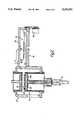
- FIG. 1is a plan view of a dual chamber processing apparatus with one form of loading mechanism
- FIG. 2is a cross-sectional view of a single chamber apparatus with a different form of loading mechanism.
- a processing apparatus 10has chambers 11 and 12 and a loading mechanism generally indicated at 13.
- the loading mechanism 13includes a carrier 14 and an actuating mechanism 15 which can move the carrier 14 in a straight line into or out of the chambers 11 and 12 using a "frog legs" mechanism.
- a "frog legs" mechanismOne example is manufactured by Brooks Automation.
- a pallet 16can be placed into the carrier 14.
- the pallet 16which has a number of recessed semi-conductor wafer locations 17 and eight slots 18 of different lengths, extending into, and in some cases through, the locations 17 from the leading edge of the pallet 16.
- a work station 19 in chamber 12has a base 20 on which is positioned an array 21 of pins 22 which are, when viewed inone direction, aligned in a series of parallel lines which are indicated atA-H.
- the wafersare loaded on the pallet 16 and the pallet 16 is placed on the carrier 14 when it is outside a chamber.
- the loaded carrieris then fed into the chamber 11 or 12.
- the base 20is then lifted so that the pins 22 move up through their respective slots 18 to lift the wafers 23 from the pallet 16 and to support them in that lifted position. Becausethe slots 18 are aligned with the lines A-H the pallet 16 can then be withdrawn from the chamber and the pins can then be lowered placing the wafers 23 onto a workpiece support table 20a. In some circumstances it maynot be necessary to lower the pins.
- the base 20may be mounted on a hydraulic ram 24 to provide the lift for the pins.
- Other suitable mechanismsmay be used and the pins may be arranged to drop back through the workpiece support table 20a within the chamber.
- FIG. 2An alternative loading mechanism 25 is illustrated in FIG. 2 and in this case the table 16 is mounted for linear movement on a guide from a load chamber 26 into a processing chamber 27.
- the loading chamberis accessiblethrough a lid 28 and the mechanism is driven by a motor 29.
Landscapes
- Engineering & Computer Science (AREA)
- Physics & Mathematics (AREA)
- Condensed Matter Physics & Semiconductors (AREA)
- General Physics & Mathematics (AREA)
- Manufacturing & Machinery (AREA)
- Computer Hardware Design (AREA)
- Microelectronics & Electronic Packaging (AREA)
- Power Engineering (AREA)
- Container, Conveyance, Adherence, Positioning, Of Wafer (AREA)
Abstract
Description
This invention relates to batch loading mechanisms and in particular, but not exclusively, to loading mechanisms for use with semi-conductor processing apparatus.
Currently semi-conductor wafers are processed either as single wafers or in batches. Batches can be loaded one at a time, or as a batch on a pallet. Loading a batch one at a time is time consuming and subjects the individual wafers in the batch to varying conditions. Those loaded earliest will have spent longer in the chamber than those loaded last. This will adversely affect the process uniformity across the batch. In extreme cases the first loaded wafers will be spoilt by the wait for the last to load, or the last to load will not be processed properly because they have not achieved the same state as those that have been loaded earlier. This is particularly the case where the process involves heating. In many processes the heat required to achieve a good process is sufficiently high as to cause undesirable side effects and damage if continued for too long. It is therefore important to achieve such a temperature but to minimise the length of time the wafers are at such temperatures. If the batch loading time is significant then either the first to load will have been subjected to excessive time-at-temperature or the last to load have had insufficient time to reach the correct temperature.
The present invention consists in a workpiece loading mechanism, comprising a work station having a plurality of lifting elements arranged in lines and means for moving the elements between the workpiece lift position and a rest position; a pallet for supporting workpieces and means for moving the pallet into and out of the work station, the pallet having a plurality of slots corresponding to the lines of the elements such that the elements can pass through the slots when the pallet is at the work station, to lift the workpieces off the pallet and such that the pallet can be withdrawn from the work station with the elements in the workpiece lift position.
Preferably the lines are substantially straight and substantially parallel. In some instances single elements may consitute a line for these purposes but at least some of the lines will include a plurality of elements. The elements may be in the form of pins. Conveniently the elements are mounted on a common base for simultaneous movement for example by means of a hydraulic ram.
The invention also consists in a gas reactor having a work station including a vacuum chamber and a mechanism as defined above for loading workpieces through a side wall thereon.
The workpieces may be semi-conductor wafers.
Although the invention has been defined above it is to be understood that it includes any inventive combination of the features set out above or in the following description.
The invention may be performed in various ways and specific embodiments will now be described, by way of example, with reference to the accompanying drawings, in which:
FIG. 1 is a plan view of a dual chamber processing apparatus with one form of loading mechanism, and
FIG. 2 is a cross-sectional view of a single chamber apparatus with a different form of loading mechanism.
Referring first to FIG. 1 aprocessing apparatus 10 haschambers 11 and 12 and a loading mechanism generally indicated at 13. The loading mechanism 13 includes acarrier 14 and anactuating mechanism 15 which can move thecarrier 14 in a straight line into or out of thechambers 11 and 12 using a "frog legs" mechanism. One example is manufactured by Brooks Automation.
As will be seen apallet 16 can be placed into thecarrier 14. Thepallet 16 which has a number of recessed semi-conductor wafer locations 17 and eightslots 18 of different lengths, extending into, and in some cases through, the locations 17 from the leading edge of thepallet 16.
As can best be seen in FIG. 2 awork station 19, inchamber 12, has abase 20 on which is positioned anarray 21 ofpins 22 which are, when viewed inone direction, aligned in a series of parallel lines which are indicated atA-H. A similar array exists in chamber 11 except the lines A-H are orthogonal to those inchamber 12.
In operation the wafers are loaded on thepallet 16 and thepallet 16 is placed on thecarrier 14 when it is outside a chamber. The loaded carrier is then fed into thechamber 11 or 12. Thebase 20 is then lifted so that thepins 22 move up through theirrespective slots 18 to lift thewafers 23 from thepallet 16 and to support them in that lifted position. Becausetheslots 18 are aligned with the lines A-H thepallet 16 can then be withdrawn from the chamber and the pins can then be lowered placing thewafers 23 onto a workpiece support table 20a. In some circumstances it maynot be necessary to lower the pins.
Unloading is exactly the reverse procedure and again theslots 18 allowthepallet 16 to pass thepins 22.
As can be seen in FIG. 2 thebase 20 may be mounted on a hydraulic ram 24 to provide the lift for the pins. Other suitable mechanisms may be used and the pins may be arranged to drop back through the workpiece support table 20a within the chamber.
Analternative loading mechanism 25 is illustrated in FIG. 2 and in this case the table 16 is mounted for linear movement on a guide from aload chamber 26 into a processing chamber 27. The loading chamber is accessiblethrough alid 28 and the mechanism is driven by a motor 29.
Claims (4)
1. A workpiece loading mechanism, comprising a work station including a treatment bed having substantially continuous workpiece receiving surface and having a plurality of lifting elements, which pass through the bed and are arranged in lines, and means for moving the elements between a workpiece lift position and a withdrawn position in which they do not project above the surface; a pallet for supporting a plurality of workpieces in respective workpiece locations disposed in an array and means for moving the pallet into and out of the work station so that in one position it overlies the bed, the pallet defining a plurality of slots open at one end corresponding to the lines of the elements such that when the pallet is in said one position each element can pass through a slot to lift the workpieces off the pallet, at least one of the slots extending through a plurality of workpiece positions and such that the pallet can be withdrawn from the work station with the elements in the workpiece lift position and the elements can then lower the workpieces on to the bed as they return to their withdrawn position.
2. A mechanism as claimed in claim 1, wherein the lines are substantially straight and substantially parallel.
3. A mechanism as claimed in claim 1, wherein the elements are in the form of pins.
4. A mechanism as claimed in claim 1, wherein the elements are mounted on a common base for simultaneous movement.
Applications Claiming Priority (3)
| Application Number | Priority Date | Filing Date | Title |
|---|---|---|---|
| GB909006471AGB9006471D0 (en) | 1990-03-22 | 1990-03-22 | Loading mechanisms |
| GB9006471.8 | 1990-03-22 | ||
| PCT/GB1991/000221WO1991015032A1 (en) | 1990-03-22 | 1991-02-14 | Loading mechanisms |
Publications (1)
| Publication Number | Publication Date |
|---|---|
| US5330301Atrue US5330301A (en) | 1994-07-19 |
Family
ID=10673087
Family Applications (1)
| Application Number | Title | Priority Date | Filing Date |
|---|---|---|---|
| US07/924,022Expired - LifetimeUS5330301A (en) | 1990-03-22 | 1991-02-14 | Loading mechanisms |
Country Status (5)
| Country | Link |
|---|---|
| US (1) | US5330301A (en) |
| EP (1) | EP0520996B1 (en) |
| DE (1) | DE69128194T2 (en) |
| GB (1) | GB9006471D0 (en) |
| WO (1) | WO1991015032A1 (en) |
Cited By (59)
| Publication number | Priority date | Publication date | Assignee | Title |
|---|---|---|---|---|
| US5430991A (en)* | 1993-04-23 | 1995-07-11 | Tandberg Data Storage | Data carrier magazine and opening mechanism |
| US6057662A (en)* | 1998-02-25 | 2000-05-02 | Applied Materials, Inc. | Single motor control for substrate handler in processing system |
| US6176668B1 (en)* | 1998-05-20 | 2001-01-23 | Applied Komatsu Technology, Inc. | In-situ substrate transfer shuttle |
| US6224312B1 (en)* | 1996-11-18 | 2001-05-01 | Applied Materials, Inc. | Optimal trajectory robot motion |
| US6290864B1 (en) | 1999-10-26 | 2001-09-18 | Reflectivity, Inc. | Fluoride gas etching of silicon with improved selectivity |
| US6332526B1 (en)* | 1999-02-17 | 2001-12-25 | Fastems Oy Ab | Loading station |
| US20020033133A1 (en)* | 2000-07-27 | 2002-03-21 | Klein Martin P. | Substrate processing pallet and related substrate processing method and machine |
| US20020195423A1 (en)* | 1999-10-26 | 2002-12-26 | Reflectivity, Inc. | Method for vapor phase etching of silicon |
| US20030054588A1 (en)* | 2000-12-07 | 2003-03-20 | Reflectivity, Inc., A California Corporation | Methods for depositing, releasing and packaging micro-electromechanical devices on wafer substrates |
| US20030073302A1 (en)* | 2001-10-12 | 2003-04-17 | Reflectivity, Inc., A California Corporation | Methods for formation of air gap interconnects |
| US20030138986A1 (en)* | 2001-09-13 | 2003-07-24 | Mike Bruner | Microelectronic mechanical system and methods |
| US20030235932A1 (en)* | 2002-05-28 | 2003-12-25 | Silicon Light Machines | Integrated driver process flow |
| US6707591B2 (en) | 2001-04-10 | 2004-03-16 | Silicon Light Machines | Angled illumination for a single order light modulator based projection system |
| US6712480B1 (en) | 2002-09-27 | 2004-03-30 | Silicon Light Machines | Controlled curvature of stressed micro-structures |
| US6714337B1 (en) | 2002-06-28 | 2004-03-30 | Silicon Light Machines | Method and device for modulating a light beam and having an improved gamma response |
| US6719516B2 (en)* | 1998-09-28 | 2004-04-13 | Applied Materials, Inc. | Single wafer load lock with internal wafer transport |
| US6728023B1 (en) | 2002-05-28 | 2004-04-27 | Silicon Light Machines | Optical device arrays with optimized image resolution |
| US6746198B2 (en) | 1998-05-20 | 2004-06-08 | Applied Materials, Inc. | Substrate transfer shuttle |
| US6747781B2 (en) | 2001-06-25 | 2004-06-08 | Silicon Light Machines, Inc. | Method, apparatus, and diffuser for reducing laser speckle |
| US6764875B2 (en) | 1998-07-29 | 2004-07-20 | Silicon Light Machines | Method of and apparatus for sealing an hermetic lid to a semiconductor die |
| US6782205B2 (en) | 2001-06-25 | 2004-08-24 | Silicon Light Machines | Method and apparatus for dynamic equalization in wavelength division multiplexing |
| US6800238B1 (en) | 2002-01-15 | 2004-10-05 | Silicon Light Machines, Inc. | Method for domain patterning in low coercive field ferroelectrics |
| US6801354B1 (en) | 2002-08-20 | 2004-10-05 | Silicon Light Machines, Inc. | 2-D diffraction grating for substantially eliminating polarization dependent losses |
| US6806997B1 (en) | 2003-02-28 | 2004-10-19 | Silicon Light Machines, Inc. | Patterned diffractive light modulator ribbon for PDL reduction |
| US6813059B2 (en) | 2002-06-28 | 2004-11-02 | Silicon Light Machines, Inc. | Reduced formation of asperities in contact micro-structures |
| US6821912B2 (en) | 2000-07-27 | 2004-11-23 | Nexx Systems Packaging, Llc | Substrate processing pallet and related substrate processing method and machine |
| US6822797B1 (en) | 2002-05-31 | 2004-11-23 | Silicon Light Machines, Inc. | Light modulator structure for producing high-contrast operation using zero-order light |
| US6829077B1 (en) | 2003-02-28 | 2004-12-07 | Silicon Light Machines, Inc. | Diffractive light modulator with dynamically rotatable diffraction plane |
| US6829258B1 (en) | 2002-06-26 | 2004-12-07 | Silicon Light Machines, Inc. | Rapidly tunable external cavity laser |
| US6829092B2 (en) | 2001-08-15 | 2004-12-07 | Silicon Light Machines, Inc. | Blazed grating light valve |
| US6847730B1 (en) | 1998-05-20 | 2005-01-25 | Applied Materials, Inc. | Automated substrate processing system |
| US6865346B1 (en) | 2001-06-05 | 2005-03-08 | Silicon Light Machines Corporation | Fiber optic transceiver |
| US20050059254A1 (en)* | 2003-09-17 | 2005-03-17 | Hongqin Shi | Methods and apparatus of etch process control in fabrications of microstructures |
| US6872984B1 (en) | 1998-07-29 | 2005-03-29 | Silicon Light Machines Corporation | Method of sealing a hermetic lid to a semiconductor die at an angle |
| US20050088718A1 (en)* | 2003-07-03 | 2005-04-28 | Patel Satyadev R. | Micromirror array having reduced gap between adjacent micromirrors of the micromirror array |
| US6908201B2 (en) | 2002-06-28 | 2005-06-21 | Silicon Light Machines Corporation | Micro-support structures |
| US6922273B1 (en) | 2003-02-28 | 2005-07-26 | Silicon Light Machines Corporation | PDL mitigation structure for diffractive MEMS and gratings |
| US6922272B1 (en) | 2003-02-14 | 2005-07-26 | Silicon Light Machines Corporation | Method and apparatus for leveling thermal stress variations in multi-layer MEMS devices |
| US6928207B1 (en) | 2002-12-12 | 2005-08-09 | Silicon Light Machines Corporation | Apparatus for selectively blocking WDM channels |
| US6927891B1 (en) | 2002-12-23 | 2005-08-09 | Silicon Light Machines Corporation | Tilt-able grating plane for improved crosstalk in 1×N blaze switches |
| US6934070B1 (en) | 2002-12-18 | 2005-08-23 | Silicon Light Machines Corporation | Chirped optical MEM device |
| US6947613B1 (en) | 2003-02-11 | 2005-09-20 | Silicon Light Machines Corporation | Wavelength selective switch and equalizer |
| US6949202B1 (en) | 1999-10-26 | 2005-09-27 | Reflectivity, Inc | Apparatus and method for flow of process gas in an ultra-clean environment |
| US6956878B1 (en) | 2000-02-07 | 2005-10-18 | Silicon Light Machines Corporation | Method and apparatus for reducing laser speckle using polarization averaging |
| US6956995B1 (en) | 2001-11-09 | 2005-10-18 | Silicon Light Machines Corporation | Optical communication arrangement |
| US6987600B1 (en) | 2002-12-17 | 2006-01-17 | Silicon Light Machines Corporation | Arbitrary phase profile for better equalization in dynamic gain equalizer |
| US7027202B1 (en) | 2003-02-28 | 2006-04-11 | Silicon Light Machines Corp | Silicon substrate as a light modulator sacrificial layer |
| US7042611B1 (en) | 2003-03-03 | 2006-05-09 | Silicon Light Machines Corporation | Pre-deflected bias ribbons |
| US7054515B1 (en) | 2002-05-30 | 2006-05-30 | Silicon Light Machines Corporation | Diffractive light modulator-based dynamic equalizer with integrated spectral monitor |
| US7057819B1 (en) | 2002-12-17 | 2006-06-06 | Silicon Light Machines Corporation | High contrast tilting ribbon blazed grating |
| US7057795B2 (en) | 2002-08-20 | 2006-06-06 | Silicon Light Machines Corporation | Micro-structures with individually addressable ribbon pairs |
| US7068372B1 (en) | 2003-01-28 | 2006-06-27 | Silicon Light Machines Corporation | MEMS interferometer-based reconfigurable optical add-and-drop multiplexor |
| US7100954B2 (en) | 2003-07-11 | 2006-09-05 | Nexx Systems, Inc. | Ultra-thin wafer handling system |
| US20060266730A1 (en)* | 2003-03-28 | 2006-11-30 | Jonathan Doan | Microelectromechanical structure and a method for making the same |
| US7177081B2 (en) | 2001-03-08 | 2007-02-13 | Silicon Light Machines Corporation | High contrast grating light valve type device |
| US7189332B2 (en) | 2001-09-17 | 2007-03-13 | Texas Instruments Incorporated | Apparatus and method for detecting an endpoint in a vapor phase etch |
| US7286764B1 (en) | 2003-02-03 | 2007-10-23 | Silicon Light Machines Corporation | Reconfigurable modulator-based optical add-and-drop multiplexer |
| US7391973B1 (en) | 2003-02-28 | 2008-06-24 | Silicon Light Machines Corporation | Two-stage gain equalizer |
| US7655092B2 (en) | 1996-11-18 | 2010-02-02 | Applied Materials, Inc. | Tandem process chamber |
Families Citing this family (2)
| Publication number | Priority date | Publication date | Assignee | Title |
|---|---|---|---|---|
| GB9524608D0 (en)* | 1995-12-01 | 1996-01-31 | Rockwool Int | Manufacture of man-made vitreous fibre products |
| DE102011050324A1 (en)* | 2011-05-12 | 2012-11-29 | Roth & Rau Ag | Substrate transport module, loading and unloading system and transport method for substrates in a substrate processing plant |
Citations (14)
| Publication number | Priority date | Publication date | Assignee | Title |
|---|---|---|---|---|
| US2274464A (en)* | 1940-11-25 | 1942-02-24 | Joe Lowe Corp | Method of and apparatus for manufacturing confectionery products |
| US2451226A (en)* | 1946-12-10 | 1948-10-12 | Jr John H Kemp | Apparatus for handling loads |
| US2856089A (en)* | 1952-05-31 | 1958-10-14 | Paul A Schilling | Means for encasing eggs |
| US3151754A (en)* | 1961-03-28 | 1964-10-06 | Jr John H Kemp | Apparatus for transferring loads |
| US3926323A (en)* | 1970-04-10 | 1975-12-16 | Packard Instrument Co Inc | Method of and apparatus for vial transferring and changing |
| EP0063289A2 (en)* | 1981-04-20 | 1982-10-27 | The Perkin-Elmer Corporation | Apparatus for aligning a wafer |
| US4534695A (en)* | 1983-05-23 | 1985-08-13 | Eaton Corporation | Wafer transport system |
| GB2156582A (en)* | 1984-03-29 | 1985-10-09 | Perkin Elmer Corp | Small part transport system |
| US4571141A (en)* | 1984-04-19 | 1986-02-18 | Metromail Corporation | Pallet unloading fixture |
| EP0211292A2 (en)* | 1985-08-09 | 1987-02-25 | Hitachi, Ltd. | Molecular beam epitaxy apparatus |
| GB2198881A (en)* | 1986-12-02 | 1988-06-22 | Teradyne Inc | Transporting wafers |
| US4856641A (en)* | 1986-11-25 | 1989-08-15 | Dainippon Screen Mfg. Co., Ltd. | Apparatus and a method for carrying wafers |
| DE3909669A1 (en)* | 1988-03-24 | 1989-10-05 | Canon Kk | DEVICE FOR MACHINING WORKPIECES |
| US5104278A (en)* | 1989-09-29 | 1992-04-14 | Atlantic Sunline Ltd. | Plug seedling extractor and method of using same |
- 1990
- 1990-03-22GBGB909006471Apatent/GB9006471D0/enactivePending
- 1991
- 1991-02-14USUS07/924,022patent/US5330301A/ennot_activeExpired - Lifetime
- 1991-02-14WOPCT/GB1991/000221patent/WO1991015032A1/enactiveIP Right Grant
- 1991-02-14EPEP91903229Apatent/EP0520996B1/ennot_activeExpired - Lifetime
- 1991-02-14DEDE69128194Tpatent/DE69128194T2/ennot_activeExpired - Fee Related
Patent Citations (14)
| Publication number | Priority date | Publication date | Assignee | Title |
|---|---|---|---|---|
| US2274464A (en)* | 1940-11-25 | 1942-02-24 | Joe Lowe Corp | Method of and apparatus for manufacturing confectionery products |
| US2451226A (en)* | 1946-12-10 | 1948-10-12 | Jr John H Kemp | Apparatus for handling loads |
| US2856089A (en)* | 1952-05-31 | 1958-10-14 | Paul A Schilling | Means for encasing eggs |
| US3151754A (en)* | 1961-03-28 | 1964-10-06 | Jr John H Kemp | Apparatus for transferring loads |
| US3926323A (en)* | 1970-04-10 | 1975-12-16 | Packard Instrument Co Inc | Method of and apparatus for vial transferring and changing |
| EP0063289A2 (en)* | 1981-04-20 | 1982-10-27 | The Perkin-Elmer Corporation | Apparatus for aligning a wafer |
| US4534695A (en)* | 1983-05-23 | 1985-08-13 | Eaton Corporation | Wafer transport system |
| GB2156582A (en)* | 1984-03-29 | 1985-10-09 | Perkin Elmer Corp | Small part transport system |
| US4571141A (en)* | 1984-04-19 | 1986-02-18 | Metromail Corporation | Pallet unloading fixture |
| EP0211292A2 (en)* | 1985-08-09 | 1987-02-25 | Hitachi, Ltd. | Molecular beam epitaxy apparatus |
| US4856641A (en)* | 1986-11-25 | 1989-08-15 | Dainippon Screen Mfg. Co., Ltd. | Apparatus and a method for carrying wafers |
| GB2198881A (en)* | 1986-12-02 | 1988-06-22 | Teradyne Inc | Transporting wafers |
| DE3909669A1 (en)* | 1988-03-24 | 1989-10-05 | Canon Kk | DEVICE FOR MACHINING WORKPIECES |
| US5104278A (en)* | 1989-09-29 | 1992-04-14 | Atlantic Sunline Ltd. | Plug seedling extractor and method of using same |
Cited By (74)
| Publication number | Priority date | Publication date | Assignee | Title |
|---|---|---|---|---|
| US5430991A (en)* | 1993-04-23 | 1995-07-11 | Tandberg Data Storage | Data carrier magazine and opening mechanism |
| US7655092B2 (en) | 1996-11-18 | 2010-02-02 | Applied Materials, Inc. | Tandem process chamber |
| US6224312B1 (en)* | 1996-11-18 | 2001-05-01 | Applied Materials, Inc. | Optimal trajectory robot motion |
| US6057662A (en)* | 1998-02-25 | 2000-05-02 | Applied Materials, Inc. | Single motor control for substrate handler in processing system |
| US6176668B1 (en)* | 1998-05-20 | 2001-01-23 | Applied Komatsu Technology, Inc. | In-situ substrate transfer shuttle |
| US6746198B2 (en) | 1998-05-20 | 2004-06-08 | Applied Materials, Inc. | Substrate transfer shuttle |
| US6847730B1 (en) | 1998-05-20 | 2005-01-25 | Applied Materials, Inc. | Automated substrate processing system |
| US6872984B1 (en) | 1998-07-29 | 2005-03-29 | Silicon Light Machines Corporation | Method of sealing a hermetic lid to a semiconductor die at an angle |
| US6764875B2 (en) | 1998-07-29 | 2004-07-20 | Silicon Light Machines | Method of and apparatus for sealing an hermetic lid to a semiconductor die |
| US6719516B2 (en)* | 1998-09-28 | 2004-04-13 | Applied Materials, Inc. | Single wafer load lock with internal wafer transport |
| US6332526B1 (en)* | 1999-02-17 | 2001-12-25 | Fastems Oy Ab | Loading station |
| US20020195423A1 (en)* | 1999-10-26 | 2002-12-26 | Reflectivity, Inc. | Method for vapor phase etching of silicon |
| US7041224B2 (en) | 1999-10-26 | 2006-05-09 | Reflectivity, Inc. | Method for vapor phase etching of silicon |
| US6290864B1 (en) | 1999-10-26 | 2001-09-18 | Reflectivity, Inc. | Fluoride gas etching of silicon with improved selectivity |
| US6949202B1 (en) | 1999-10-26 | 2005-09-27 | Reflectivity, Inc | Apparatus and method for flow of process gas in an ultra-clean environment |
| US6956878B1 (en) | 2000-02-07 | 2005-10-18 | Silicon Light Machines Corporation | Method and apparatus for reducing laser speckle using polarization averaging |
| US20020033133A1 (en)* | 2000-07-27 | 2002-03-21 | Klein Martin P. | Substrate processing pallet and related substrate processing method and machine |
| US6682288B2 (en)* | 2000-07-27 | 2004-01-27 | Nexx Systems Packaging, Llc | Substrate processing pallet and related substrate processing method and machine |
| US6821912B2 (en) | 2000-07-27 | 2004-11-23 | Nexx Systems Packaging, Llc | Substrate processing pallet and related substrate processing method and machine |
| US6969635B2 (en) | 2000-12-07 | 2005-11-29 | Reflectivity, Inc. | Methods for depositing, releasing and packaging micro-electromechanical devices on wafer substrates |
| US20030054588A1 (en)* | 2000-12-07 | 2003-03-20 | Reflectivity, Inc., A California Corporation | Methods for depositing, releasing and packaging micro-electromechanical devices on wafer substrates |
| US7177081B2 (en) | 2001-03-08 | 2007-02-13 | Silicon Light Machines Corporation | High contrast grating light valve type device |
| US6707591B2 (en) | 2001-04-10 | 2004-03-16 | Silicon Light Machines | Angled illumination for a single order light modulator based projection system |
| US6865346B1 (en) | 2001-06-05 | 2005-03-08 | Silicon Light Machines Corporation | Fiber optic transceiver |
| US6747781B2 (en) | 2001-06-25 | 2004-06-08 | Silicon Light Machines, Inc. | Method, apparatus, and diffuser for reducing laser speckle |
| US6782205B2 (en) | 2001-06-25 | 2004-08-24 | Silicon Light Machines | Method and apparatus for dynamic equalization in wavelength division multiplexing |
| US6829092B2 (en) | 2001-08-15 | 2004-12-07 | Silicon Light Machines, Inc. | Blazed grating light valve |
| US6930364B2 (en) | 2001-09-13 | 2005-08-16 | Silicon Light Machines Corporation | Microelectronic mechanical system and methods |
| US7049164B2 (en) | 2001-09-13 | 2006-05-23 | Silicon Light Machines Corporation | Microelectronic mechanical system and methods |
| US20030138986A1 (en)* | 2001-09-13 | 2003-07-24 | Mike Bruner | Microelectronic mechanical system and methods |
| US20040053434A1 (en)* | 2001-09-13 | 2004-03-18 | Silicon Light Machines | Microelectronic mechanical system and methods |
| US7189332B2 (en) | 2001-09-17 | 2007-03-13 | Texas Instruments Incorporated | Apparatus and method for detecting an endpoint in a vapor phase etch |
| US20070119814A1 (en)* | 2001-09-17 | 2007-05-31 | Texas Instruments Incorporated | Apparatus and method for detecting an endpoint in a vapor phase etch |
| US20030073302A1 (en)* | 2001-10-12 | 2003-04-17 | Reflectivity, Inc., A California Corporation | Methods for formation of air gap interconnects |
| US6956995B1 (en) | 2001-11-09 | 2005-10-18 | Silicon Light Machines Corporation | Optical communication arrangement |
| US6800238B1 (en) | 2002-01-15 | 2004-10-05 | Silicon Light Machines, Inc. | Method for domain patterning in low coercive field ferroelectrics |
| US6728023B1 (en) | 2002-05-28 | 2004-04-27 | Silicon Light Machines | Optical device arrays with optimized image resolution |
| US20030235932A1 (en)* | 2002-05-28 | 2003-12-25 | Silicon Light Machines | Integrated driver process flow |
| US6767751B2 (en) | 2002-05-28 | 2004-07-27 | Silicon Light Machines, Inc. | Integrated driver process flow |
| US7054515B1 (en) | 2002-05-30 | 2006-05-30 | Silicon Light Machines Corporation | Diffractive light modulator-based dynamic equalizer with integrated spectral monitor |
| US6822797B1 (en) | 2002-05-31 | 2004-11-23 | Silicon Light Machines, Inc. | Light modulator structure for producing high-contrast operation using zero-order light |
| US6829258B1 (en) | 2002-06-26 | 2004-12-07 | Silicon Light Machines, Inc. | Rapidly tunable external cavity laser |
| US6908201B2 (en) | 2002-06-28 | 2005-06-21 | Silicon Light Machines Corporation | Micro-support structures |
| US6714337B1 (en) | 2002-06-28 | 2004-03-30 | Silicon Light Machines | Method and device for modulating a light beam and having an improved gamma response |
| US6813059B2 (en) | 2002-06-28 | 2004-11-02 | Silicon Light Machines, Inc. | Reduced formation of asperities in contact micro-structures |
| US6801354B1 (en) | 2002-08-20 | 2004-10-05 | Silicon Light Machines, Inc. | 2-D diffraction grating for substantially eliminating polarization dependent losses |
| US7057795B2 (en) | 2002-08-20 | 2006-06-06 | Silicon Light Machines Corporation | Micro-structures with individually addressable ribbon pairs |
| US6712480B1 (en) | 2002-09-27 | 2004-03-30 | Silicon Light Machines | Controlled curvature of stressed micro-structures |
| US6928207B1 (en) | 2002-12-12 | 2005-08-09 | Silicon Light Machines Corporation | Apparatus for selectively blocking WDM channels |
| US6987600B1 (en) | 2002-12-17 | 2006-01-17 | Silicon Light Machines Corporation | Arbitrary phase profile for better equalization in dynamic gain equalizer |
| US7057819B1 (en) | 2002-12-17 | 2006-06-06 | Silicon Light Machines Corporation | High contrast tilting ribbon blazed grating |
| US6934070B1 (en) | 2002-12-18 | 2005-08-23 | Silicon Light Machines Corporation | Chirped optical MEM device |
| US6927891B1 (en) | 2002-12-23 | 2005-08-09 | Silicon Light Machines Corporation | Tilt-able grating plane for improved crosstalk in 1×N blaze switches |
| US7068372B1 (en) | 2003-01-28 | 2006-06-27 | Silicon Light Machines Corporation | MEMS interferometer-based reconfigurable optical add-and-drop multiplexor |
| US7286764B1 (en) | 2003-02-03 | 2007-10-23 | Silicon Light Machines Corporation | Reconfigurable modulator-based optical add-and-drop multiplexer |
| US6947613B1 (en) | 2003-02-11 | 2005-09-20 | Silicon Light Machines Corporation | Wavelength selective switch and equalizer |
| US6922272B1 (en) | 2003-02-14 | 2005-07-26 | Silicon Light Machines Corporation | Method and apparatus for leveling thermal stress variations in multi-layer MEMS devices |
| US6829077B1 (en) | 2003-02-28 | 2004-12-07 | Silicon Light Machines, Inc. | Diffractive light modulator with dynamically rotatable diffraction plane |
| US7027202B1 (en) | 2003-02-28 | 2006-04-11 | Silicon Light Machines Corp | Silicon substrate as a light modulator sacrificial layer |
| US6922273B1 (en) | 2003-02-28 | 2005-07-26 | Silicon Light Machines Corporation | PDL mitigation structure for diffractive MEMS and gratings |
| US6806997B1 (en) | 2003-02-28 | 2004-10-19 | Silicon Light Machines, Inc. | Patterned diffractive light modulator ribbon for PDL reduction |
| US7391973B1 (en) | 2003-02-28 | 2008-06-24 | Silicon Light Machines Corporation | Two-stage gain equalizer |
| US7042611B1 (en) | 2003-03-03 | 2006-05-09 | Silicon Light Machines Corporation | Pre-deflected bias ribbons |
| US20060266730A1 (en)* | 2003-03-28 | 2006-11-30 | Jonathan Doan | Microelectromechanical structure and a method for making the same |
| US7153443B2 (en) | 2003-03-28 | 2006-12-26 | Texas Instruments Incorporated | Microelectromechanical structure and a method for making the same |
| US20050088718A1 (en)* | 2003-07-03 | 2005-04-28 | Patel Satyadev R. | Micromirror array having reduced gap between adjacent micromirrors of the micromirror array |
| US6985277B2 (en) | 2003-07-03 | 2006-01-10 | Reflectivity, Inc | Micromirror array having reduced gap between adjacent micromirrors of the micromirror array |
| US6970281B2 (en) | 2003-07-03 | 2005-11-29 | Reflectivity, Inc. | Micromirror array having reduced gap between adjacent micromirrors of the micromirror array |
| US6965468B2 (en) | 2003-07-03 | 2005-11-15 | Reflectivity, Inc | Micromirror array having reduced gap between adjacent micromirrors of the micromirror array |
| US20050231788A1 (en)* | 2003-07-03 | 2005-10-20 | Andrew Huibers | Micromirror array having reduced gap between adjacent micromirrors of the micromirror array |
| US20050122561A1 (en)* | 2003-07-03 | 2005-06-09 | Andrew Huibers | Micromirror array having reduced gap between adjacent micromirrors of the micromirror array |
| US7100954B2 (en) | 2003-07-11 | 2006-09-05 | Nexx Systems, Inc. | Ultra-thin wafer handling system |
| US7645704B2 (en) | 2003-09-17 | 2010-01-12 | Texas Instruments Incorporated | Methods and apparatus of etch process control in fabrications of microstructures |
| US20050059254A1 (en)* | 2003-09-17 | 2005-03-17 | Hongqin Shi | Methods and apparatus of etch process control in fabrications of microstructures |
Also Published As
| Publication number | Publication date |
|---|---|
| EP0520996B1 (en) | 1997-11-12 |
| DE69128194D1 (en) | 1997-12-18 |
| EP0520996A1 (en) | 1993-01-07 |
| WO1991015032A1 (en) | 1991-10-03 |
| GB9006471D0 (en) | 1990-05-23 |
| DE69128194T2 (en) | 1998-03-26 |
Similar Documents
| Publication | Publication Date | Title |
|---|---|---|
| US5330301A (en) | Loading mechanisms | |
| JP2913439B2 (en) | Transfer device and transfer method | |
| CN100362620C (en) | Semiconductor process part loading and unloading device and its loading and unloading method | |
| KR100233310B1 (en) | Heat treatment equipment | |
| KR102157427B1 (en) | Substrate transfer robot and substrate processing system | |
| US7570876B2 (en) | Method and system for loading substrate supports into a substrate holder | |
| US3272350A (en) | Method and apparatus for semiconductor wafer handling | |
| KR102355962B1 (en) | An apparatus for transferring a substrate, a processing apparatus having a receiving plate adapted to a substrate carrier of such apparatus, a method of processing a substrate using such apparatus for transferring a substrate, and a processing system | |
| US4938655A (en) | Wafer transfer method | |
| KR0148383B1 (en) | Carrier stalker | |
| KR19990007411A (en) | Board Transfer Device | |
| KR0147387B1 (en) | Vertical heat treating apparatus | |
| US5435686A (en) | Bearing race hardening line | |
| US5970807A (en) | Tweezer position checker | |
| JP2662982B2 (en) | Heating equipment | |
| US8936462B2 (en) | Multi-operation wafer baking system | |
| JP2630366B2 (en) | Loading / unloading method and loading / unloading device for plate-like body | |
| JP2600206B2 (en) | Vertical heat treatment equipment | |
| JP2592310B2 (en) | Processing equipment | |
| KR20240015555A (en) | Oven magazine transfer apparatus | |
| KR0133679B1 (en) | Processing unit | |
| KR100375866B1 (en) | Process and device for treating substrates in a fluid container | |
| JP2617790B2 (en) | Processing method | |
| JPH0370154A (en) | Transfer method | |
| KR100220817B1 (en) | A cvd apparatus |
Legal Events
| Date | Code | Title | Description |
|---|---|---|---|
| AS | Assignment | Owner name:SURFACE TECHNOLOGY SYSTEMS LIMITED, UNITED KINGDOM Free format text:ASSIGNMENT OF ASSIGNORS INTEREST.;ASSIGNOR:BRANCHER, CARL D. M.;REEL/FRAME:006354/0344 Effective date:19920817 | |
| STCF | Information on status: patent grant | Free format text:PATENTED CASE | |
| FPAY | Fee payment | Year of fee payment:4 | |
| SULP | Surcharge for late payment | ||
| FEPP | Fee payment procedure | Free format text:PAYOR NUMBER ASSIGNED (ORIGINAL EVENT CODE: ASPN); ENTITY STATUS OF PATENT OWNER: SMALL ENTITY | |
| FPAY | Fee payment | Year of fee payment:8 | |
| FPAY | Fee payment | Year of fee payment:12 |