US5329153A - Antifuse with nonstoichiometric tin layer and method of manufacture thereof - Google Patents
Antifuse with nonstoichiometric tin layer and method of manufacture thereofDownload PDFInfo
- Publication number
- US5329153A US5329153AUS07/866,037US86603792AUS5329153AUS 5329153 AUS5329153 AUS 5329153AUS 86603792 AUS86603792 AUS 86603792AUS 5329153 AUS5329153 AUS 5329153A
- Authority
- US
- United States
- Prior art keywords
- layer
- antifuse
- tin
- barrier metal
- conducting
- Prior art date
- Legal status (The legal status is an assumption and is not a legal conclusion. Google has not performed a legal analysis and makes no representation as to the accuracy of the status listed.)
- Expired - Lifetime
Links
Images

Classifications
- H—ELECTRICITY
- H01—ELECTRIC ELEMENTS
- H01L—SEMICONDUCTOR DEVICES NOT COVERED BY CLASS H10
- H01L23/00—Details of semiconductor or other solid state devices
- H01L23/52—Arrangements for conducting electric current within the device in operation from one component to another, i.e. interconnections, e.g. wires, lead frames
- H01L23/522—Arrangements for conducting electric current within the device in operation from one component to another, i.e. interconnections, e.g. wires, lead frames including external interconnections consisting of a multilayer structure of conductive and insulating layers inseparably formed on the semiconductor body
- H01L23/532—Arrangements for conducting electric current within the device in operation from one component to another, i.e. interconnections, e.g. wires, lead frames including external interconnections consisting of a multilayer structure of conductive and insulating layers inseparably formed on the semiconductor body characterised by the materials
- H01L23/53204—Conductive materials
- H01L23/53271—Conductive materials containing semiconductor material, e.g. polysilicon
- H—ELECTRICITY
- H01—ELECTRIC ELEMENTS
- H01L—SEMICONDUCTOR DEVICES NOT COVERED BY CLASS H10
- H01L23/00—Details of semiconductor or other solid state devices
- H01L23/52—Arrangements for conducting electric current within the device in operation from one component to another, i.e. interconnections, e.g. wires, lead frames
- H01L23/522—Arrangements for conducting electric current within the device in operation from one component to another, i.e. interconnections, e.g. wires, lead frames including external interconnections consisting of a multilayer structure of conductive and insulating layers inseparably formed on the semiconductor body
- H01L23/525—Arrangements for conducting electric current within the device in operation from one component to another, i.e. interconnections, e.g. wires, lead frames including external interconnections consisting of a multilayer structure of conductive and insulating layers inseparably formed on the semiconductor body with adaptable interconnections
- H01L23/5252—Arrangements for conducting electric current within the device in operation from one component to another, i.e. interconnections, e.g. wires, lead frames including external interconnections consisting of a multilayer structure of conductive and insulating layers inseparably formed on the semiconductor body with adaptable interconnections comprising anti-fuses, i.e. connections having their state changed from non-conductive to conductive
- H—ELECTRICITY
- H01—ELECTRIC ELEMENTS
- H01L—SEMICONDUCTOR DEVICES NOT COVERED BY CLASS H10
- H01L2924/00—Indexing scheme for arrangements or methods for connecting or disconnecting semiconductor or solid-state bodies as covered by H01L24/00
- H01L2924/0001—Technical content checked by a classifier
- H01L2924/0002—Not covered by any one of groups H01L24/00, H01L24/00 and H01L2224/00
Definitions
- the present inventionis related to integrated circuit structure and processing technology and, more particularly, to antifuses in integrated circuits and their manufacture.
- Antifusesare found in a growing number of integrated circuits, most of which are field programmable gate arrays (FPGAs). As the name implies, antifuses have a very high resistance (to form essentially an open circuit) in the unprogrammed (“off") state, and a very low resistance (to form essentially a closed circuit in the programmed ("on") state. In these integrated circuits antifuses are placed at the intersections of interconnection lines which lead to different elements of the integrated circuit. By programming selected antifuses, the interconnections between the various elements of the integrated circuit are formed to define the function of the device.
- FPGAsfield programmable gate arrays
- Antifuseshave various structures.
- One particular antifuse structureis described in U.S. Ser. No. 07/642,617, entitled "AN IMPROVED ANTIFUSE CIRCUIT STRUCTURE FOR USE IN A FIELD PROGRAMMABLE GATE ARRAY AND METHOD OF MANUFACTURE THEREOF," filed Jan. 17, 1991 by M. R. Holzworth et al. and assigned to the assignee of the present invention.
- a semiconductor layer of amorphous siliconis sandwiched between two metal interconnection lines.
- a layer of TiWtitanium-tungsten forms a barrier metal layer between the semiconductor layer and each metal interconnection layer.
- Barrier metal layersfunction to block the undesired interdiffusion of a semiconductor layer and a metal layer, which, in the case of the described antifuse, is the amorphous silicon layer and each interconnection layer formed from aluminum alloy.
- Barrier metal layersare typically refractory metals, their intermetallics, alloys, silicides, nitrides and combinations thereof.
- a typical barrier metal layeris TiN (titanium nitride).
- antifuses formed with TiN barrier metal layershave a discernable probability of having an undesirably high programmed resistance (R ON ).
- R ONprogrammed resistance
- TiN processesare familiar to many integrated circuit manufacturers and commonly used by them. This familiarity and use makes such manufacturers reluctant to abandon their TiN process in order to implement the antifuse structure.
- semiconductor processing technologyit is a general rule that manufacturers are reluctant to substitute any process for another due to cost and time constraints.
- the present inventionaddresses this problem of TiN barrier metal layers in antifuses and provides for a solution by which TiN barrier metal processing technology may be adapted for use in manufacturing antifuses in integrated circuits without the problem described above.
- the present inventionprovides for an antifuse in an integrated circuit which has first and second conducting lines, a semiconductor layer of amorphous silicon between the first and second conducting lines, and a barrier metal layer of TiN between the semiconductor layer and the first conducting layer.
- the TiN layeris a nonstoichiometric composition to enhance the probability of said antifuse having a desired resistance when said antifuse is programmed. More specifically, the TiN layer has a composition of Ti 1 .0 N 0 .5-0.8.
- the present inventionalso provides for a method of forming an antifuse in an integrated circuit which has an insulating layer on a semiconductor substrate.
- An amorphous silicon layeris formed on the first barrier metal layer, followed by the formation of a second barrier metal layer on the amorphous silicon layer.
- a second metal interconnection layeris formed on said second barrier metal layer.
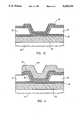
- FIGS. 1A-1Cshow a sequence of steps used to manufacture an antifuse structure
- FIG. 2is a cross-sectional diagram illustrating the resulting antifuse structure of the process steps shown in FIGS. 1A-1C.
- TiN barrier layersare described in the context of an embodiment of the particular antifuse disclosed in the above-noted patent application. However, as will be evident, the solution provided by the present invention is not necessarily limited to the particular antifuse discussed.
- FIG. 1Ashows the step in the manufacturing process after the transistors and other circuit structures have been created in a semiconductor substrate and one or more polysilicon layers with intermediate insulating silicon dioxide layers have been deposited and defined.
- a representative layer 30 of silicon dioxideis deposited over the substrate (not shown). Through standard masking and etching procedures, apertures are created in the layer 30. Then a metal layer 21 of aluminum is deposited. This is followed by a barrier metal layer 22.
- the layers 21 and 22are masked and etched by standard semiconductor processing techniques.
- the metal layers 21 and 22are in physical and electrical contact to various points in the underlying parts of the integrated circuit through the apertures in the insulating layer 30.
- insulating layer 31 of silicon dioxideis deposited over the substrate and the layers 21 and 22.
- a contact hole 29is formed in the silicon dioxide layer 31 where an antifuse is desired by conventional masking and etching procedures.
- a semiconductor material layer 23 of amorphous siliconis deposited and defined by standard masking and etching steps so that a portion of the layer 23 covers the contact hole 29.
- the amorphous siliconmay be doped or undoped.
- a thickness in the range of 500 to 1500 Angstromshas been found to work quite well in the antifuse structure, with an thickness of approximately 800 Angstroms being optimal. These thicknesses are applicable when 10 to 15 V programming voltage is used. For substantially different programming voltages film thicknesses change accordingly. The results are shown in FIG. 1B.
- the deposition of the amorphous silicon layer 23should be performed at temperatures below 450 degrees C.
- Plasma-enhanced chemical vapor deposition (PECVD) and sputter depositionmay be used to deposit amorphous silicon at such comparatively low temperatures.
- LPCVDlow pressure chemical vapor deposition
- the hydrogen content of the amorphous silicon layer 23be kept in the range of 10-20% by composition so that the layer 23 has the optimum characteristics suitable for an antifuse.
- thisis achieved by increasing the flow of the inert gas, argon, over its nominal flow rate in the process or adjusting the temperature of deposition.
- a second layer 24 of barrier metalis deposited. This is followed by the deposition of the second interconnecting aluminum layer 25. Both metal layers 24 and 25 are then defined by standard masking and etching techniques. The completed antifuse structure is illustrated in FIG. 2.
- the antifuseis formed between two metal interconnection layers 21 and 25 located above the surface of the integrated circuit substrate.
- these metal interconnection layersare formed from aluminum alloys.
- the antifuse structuremay be formed between any two metal interconnection layers. In a double-metal process, for example, these layers 21 and 25 are the metal-1 and metal-2 layers.
- first barrier metal layer 22in contact with the lower metal layer 21, a layer 23 of semiconductor material, amorphous silicon, and a second barrier metal layer 24 in contact with the upper metal layer 25.
- barrier metal layers 22 and 24respectively contact the lower and upper surfaces of the amorphous silicon layer 23 which is formed with a thickness of approximately 800 Angstroms.
- the amorphous silicon layer 23acts as an insulating layer between the conducting layers 21 and 25 unless the antifuse is programmed. When the antifuse is programmed, a conductive link is formed through the amorphous silicon layer 23 and a very low resistance contact is formed between the interconnection layers 21 and 25.
- a low programmed resistance (R ON ) of 100 ohmsis typically obtained with a normal distribution about this mean value. Virtually no R ON is greater than 200 ohms. Programming is performed by a 10 mA, 5 ms pulse between the two conducting layers 21, 25.
- the R ON distributionchanges. While most of the programmed antifuses have an R ON value of 100 ohms, a substantial number of antifuses, 10-20 percent, have a R ON value of greater than 200 ohms. This is troubling because the distribution of programmed resistances of the antifuses should be within a specified range or the circuit behavior unacceptably varies from die to die.
- the present inventionmodifies the composition of TiN to a nonstoichiometric titanium nitride layer, i.e., from Ti 1 .0 N 1 .0 to Ti 1 .0 N 0 .5-0.8.
- a nonstoichiometric titanium nitride layeri.e., from Ti 1 .0 N 1 .0 to Ti 1 .0 N 0 .5-0.8.
- semiconductor processeshave used stoichiometric titanium nitride (Ti 1 .0 N 1 .0) layers, which have many properties suitable for barrier metal functions.
- the nonstoichiometric TiN layeris required to be located on the side of the amorphous silicon layer opposite the conducting layer which has a positive voltage with respect to the second conducting layer during the programming of the antifuse.
- the barrier metal layer 22should be nonstoichiometric if the aluminum layer 25 is positive with respect to the aluminum layer 21 during programming.
- the barrier metal layer 24 for the layer 25is not required to be nonstoichiometric if the layer 24 is formed from titanium nitride. The reason for the location of the nonstoichiometric TiN layer with respect to the polarity of programming voltages is stated below.
- a titanium nitride layer of Ti 1 .0 N 0 .5-0.8 stoichiometryworks very well in enhancing the statistical distribution of programmed resistances. It is believed that the reason for this effectiveness is as follows. With TiW barrier metal layers, an antifuse is programmed when the titanium and/or tungsten atoms physically move into the amorphous silicon layer. The metal atoms react with amorphous silicon layer to form a conductive silicide link between the two conducting layers. When one of the barrier metal layers (and its respective conducting layer) has a positive potential, metal atoms move from the second barrier metal layer.
- the electric breakdown potentiali.e., the programming voltage
- a tremendous electron windis generated from the second barrier metal toward the first barrier metal layer.
- the electron windalso carries along the positively charged atoms present in the second barrier metal layer, such as Ti and W. Since titanium is a lighter element, at atomic number 22, it is much more easily transportable than tungsten at atomic number 74.
- silicide linkis the conduction path between the two barrier metal (and interconnection) layers.
- the diameter of the silicide linkwhich is correlated to the programming current, is also correlated to the R ON of the antifuse.
- both Ti and Ware bonded to each other weakly by sharing outer d-orbital electrons. These bonds can be very easily broken by a fairly small amount of energy. Therefore, both Ti and W are readily available in atomic form. It is, therefore, quite easy to form the silicide link and achieve a consistent R ON for the programmed antifuses.
- the amount of free titanium available for forming the silicide links in the amorphous silicon layercan be controlled by the stoichiometry of the TiN barrier metal layer, i.e., by lowering the fraction X in the nonstoichiometric Ti 1 .0 N X layer, the amount of free titanium is increased.
- the TiN deposition equipmentis restricted to yielding only a certain ratio of Ti and N in the nonstoichiometric layer (i.e., X has a floor)
- the total amount of free Tican be obtained by adjusting the thickness of the TiN layer. More free titanium is available with a thicker layer of nonstoichiometric TiN layer.
- Nonstoichiometric TiNis obtained by modifying a standard process for depositing stoichiometric titanium nitride. Such a standard process is performed by sputtering titanium atoms from a titanium target onto a semiconductor wafer in a sputtering chamber filled with a predetermined nitrogen gas mixture, typically Ar:N 2 , at a predetermined temperature and power. A nonstoichiometric TiN layer is deposited on the wafer by reducing the deposition temperature, reducing the N 2 ratio in the gas mixture, increasing the deposition power, or a combination of these steps.
- a predetermined nitrogen gas mixturetypically Ar:N 2
Landscapes
- Physics & Mathematics (AREA)
- Condensed Matter Physics & Semiconductors (AREA)
- General Physics & Mathematics (AREA)
- Engineering & Computer Science (AREA)
- Computer Hardware Design (AREA)
- Microelectronics & Electronic Packaging (AREA)
- Power Engineering (AREA)
- Design And Manufacture Of Integrated Circuits (AREA)
- Internal Circuitry In Semiconductor Integrated Circuit Devices (AREA)
Abstract
Description
Claims (13)
Priority Applications (1)
| Application Number | Priority Date | Filing Date | Title |
|---|---|---|---|
| US07/866,037US5329153A (en) | 1992-04-10 | 1992-04-10 | Antifuse with nonstoichiometric tin layer and method of manufacture thereof |
Applications Claiming Priority (1)
| Application Number | Priority Date | Filing Date | Title |
|---|---|---|---|
| US07/866,037US5329153A (en) | 1992-04-10 | 1992-04-10 | Antifuse with nonstoichiometric tin layer and method of manufacture thereof |
Publications (1)
| Publication Number | Publication Date |
|---|---|
| US5329153Atrue US5329153A (en) | 1994-07-12 |
Family
ID=25346798
Family Applications (1)
| Application Number | Title | Priority Date | Filing Date |
|---|---|---|---|
| US07/866,037Expired - LifetimeUS5329153A (en) | 1992-04-10 | 1992-04-10 | Antifuse with nonstoichiometric tin layer and method of manufacture thereof |
Country Status (1)
| Country | Link |
|---|---|
| US (1) | US5329153A (en) |
Cited By (56)
| Publication number | Priority date | Publication date | Assignee | Title |
|---|---|---|---|---|
| WO1995027309A1 (en)* | 1994-03-31 | 1995-10-12 | Crosspoint Solutions, Inc. | A multilayered antifuse with intermediate metal layer and method of manufacture therefor |
| US5485032A (en)* | 1992-12-18 | 1996-01-16 | International Business Machines Corporation | Antifuse element with electrical or optical programming |
| US5519248A (en)* | 1993-07-07 | 1996-05-21 | Actel Corporation | Circuits for ESD protection of metal-to-metal antifuses during processing |
| US5537108A (en)* | 1994-02-08 | 1996-07-16 | Prolinx Labs Corporation | Method and structure for programming fuses |
| US5543656A (en)* | 1990-04-12 | 1996-08-06 | Actel Corporation | Metal to metal antifuse |
| EP0680087A3 (en)* | 1994-04-28 | 1996-10-02 | Canon Kk | Semiconductor device using a silicide reaction for the manufacture of adaptable interconnects. |
| US5572409A (en) | 1994-02-08 | 1996-11-05 | Prolinx Labs Corporation | Apparatus including a programmable socket adapter for coupling an electronic component to a component socket on a printed circuit board |
| US5576576A (en)* | 1992-11-04 | 1996-11-19 | Actel Corporation | Above via metal-to-metal antifuse |
| US5581111A (en)* | 1993-07-07 | 1996-12-03 | Actel Corporation | Dielectric-polysilicon-dielectric antifuse for field programmable logic applications |
| US5592016A (en)* | 1995-04-14 | 1997-01-07 | Actel Corporation | Antifuse with improved antifuse material |
| US5629227A (en)* | 1993-07-07 | 1997-05-13 | Actel Corporation | Process of making ESD protection devices for use with antifuses |
| US5633189A (en)* | 1994-08-01 | 1997-05-27 | Actel Corporation | Method of making metal to metal antifuse |
| US5639684A (en)* | 1994-01-06 | 1997-06-17 | Texas Instruments Incorporated | Method of making a low capacitance antifuse having a pillar located between the first and second metal layers |
| US5663591A (en)* | 1995-02-14 | 1997-09-02 | Crosspoint Solutions, Inc. | Antifuse with double via, spacer-defined contact |
| US5670818A (en)* | 1990-04-12 | 1997-09-23 | Actel Corporation | Electrically programmable antifuse |
| US5726482A (en) | 1994-02-08 | 1998-03-10 | Prolinx Labs Corporation | Device-under-test card for a burn-in board |
| US5741720A (en)* | 1995-10-04 | 1998-04-21 | Actel Corporation | Method of programming an improved metal-to-metal via-type antifuse |
| US5741462A (en) | 1995-04-25 | 1998-04-21 | Irori | Remotely programmable matrices with memories |
| US5751629A (en) | 1995-04-25 | 1998-05-12 | Irori | Remotely programmable matrices with memories |
| US5753528A (en)* | 1992-02-26 | 1998-05-19 | Actel Corporation | Method of fabricating metal-to-metal antifuse with improved diffusion barrier layer |
| US5763299A (en)* | 1995-06-06 | 1998-06-09 | Actel Corporation | Reduced leakage antifuse fabrication method |
| US5767575A (en) | 1995-10-17 | 1998-06-16 | Prolinx Labs Corporation | Ball grid array structure and method for packaging an integrated circuit chip |
| US5770885A (en)* | 1990-04-12 | 1998-06-23 | Actel Corporation | Electrically programmable antifuse incorporating dielectric and amorphous silicon interlayers |
| US5804500A (en)* | 1995-06-02 | 1998-09-08 | Actel Corporation | Fabrication process for raised tungsten plug antifuse |
| US5808351A (en) | 1994-02-08 | 1998-09-15 | Prolinx Labs Corporation | Programmable/reprogramable structure using fuses and antifuses |
| US5813881A (en) | 1994-02-08 | 1998-09-29 | Prolinx Labs Corporation | Programmable cable and cable adapter using fuses and antifuses |
| US5834824A (en) | 1994-02-08 | 1998-11-10 | Prolinx Labs Corporation | Use of conductive particles in a nonconductive body as an integrated circuit antifuse |
| US5856234A (en)* | 1993-09-14 | 1999-01-05 | Actel Corporation | Method of fabricating an antifuse |
| US5872338A (en) | 1996-04-10 | 1999-02-16 | Prolinx Labs Corporation | Multilayer board having insulating isolation rings |
| US5874214A (en) | 1995-04-25 | 1999-02-23 | Irori | Remotely programmable matrices with memories |
| US5899707A (en)* | 1996-08-20 | 1999-05-04 | Vlsi Technology, Inc. | Method for making doped antifuse structures |
| US5906043A (en) | 1995-01-18 | 1999-05-25 | Prolinx Labs Corporation | Programmable/reprogrammable structure using fuses and antifuses |
| US5906042A (en) | 1995-10-04 | 1999-05-25 | Prolinx Labs Corporation | Method and structure to interconnect traces of two conductive layers in a printed circuit board |
| US5917229A (en) | 1994-02-08 | 1999-06-29 | Prolinx Labs Corporation | Programmable/reprogrammable printed circuit board using fuse and/or antifuse as interconnect |
| US6001693A (en)* | 1994-10-06 | 1999-12-14 | Yeouchung; Yen | Method of making a metal to metal antifuse |
| US6017496A (en) | 1995-06-07 | 2000-01-25 | Irori | Matrices with memories and uses thereof |
| US6034427A (en) | 1998-01-28 | 2000-03-07 | Prolinx Labs Corporation | Ball grid array structure and method for packaging an integrated circuit chip |
| US6111302A (en) | 1993-11-22 | 2000-08-29 | Actel Corporation | Antifuse structure suitable for VLSI application |
| US6171512B1 (en) | 1991-02-15 | 2001-01-09 | Canon Kabushiki Kaisha | Etching solution for etching porous silicon, etching method using the etching solution and method of preparing semiconductor member using the etching solution |
| US6245631B1 (en)* | 1999-12-06 | 2001-06-12 | Micron Technology, Inc. | Method of forming buried bit line memory circuitry and semiconductor processing method of forming a conductive line |
| US6329139B1 (en) | 1995-04-25 | 2001-12-11 | Discovery Partners International | Automated sorting system for matrices with memory |
| US6331273B1 (en) | 1995-04-25 | 2001-12-18 | Discovery Partners International | Remotely programmable matrices with memories |
| US6337151B1 (en)* | 1999-08-18 | 2002-01-08 | International Business Machines Corporation | Graded composition diffusion barriers for chip wiring applications |
| US6368962B2 (en) | 1999-12-06 | 2002-04-09 | Micron Technology, Inc. | Semiconductor processing method of forming a conductive line, and buried bit line memory circuitry |
| US6416714B1 (en) | 1995-04-25 | 2002-07-09 | Discovery Partners International, Inc. | Remotely programmable matrices with memories |
| US6563189B1 (en)* | 2001-06-06 | 2003-05-13 | National Semiconductor Corporation | Method of adding Zener zap aluminum bridged anti-fuses to a tungsten plug process |
| US6768185B2 (en)* | 2000-12-22 | 2004-07-27 | Matrix Semiconductor, Inc. | Formation of antifuse structure in a three dimensional memory |
| US20040262702A1 (en)* | 2003-06-30 | 2004-12-30 | Matrix Semiconductor, Inc. | Low-density, high-resistivity titanium nitride layer for use as a contact for low-leakage dielectric layers |
| US20050090047A1 (en)* | 2000-12-20 | 2005-04-28 | Actel Corporation, A California Corporation. | Method of making a MOS transistor having improved total radiation-induced leakage current |
| US20050090073A1 (en)* | 2000-12-20 | 2005-04-28 | Actel Corporation, A California Corporation | MOS transistor having improved total radiation-induced leakage current |
| US7015076B1 (en)* | 2004-03-01 | 2006-03-21 | Advanced Micro Devices, Inc. | Selectable open circuit and anti-fuse element, and fabrication method therefor |
| US20070145524A1 (en)* | 2005-12-28 | 2007-06-28 | Dongbu Electronics Co., Ltd. | FPGA structure provided with multi parallel structure and method for forming the same |
| US20070152338A1 (en)* | 2005-12-29 | 2007-07-05 | Dongbu Electronics Co., Ltd. | Method of forming FPGA of multi-parallel structure and FPGA structure thereof |
| US20100134024A1 (en)* | 2008-11-30 | 2010-06-03 | Cree, Inc. | Led thermal management system and method |
| US20100134176A1 (en)* | 2008-11-30 | 2010-06-03 | Cree, Inc. | Electronic device including circuitry comprising open failure-susceptible components, and open failure-actuated anti-fuse pathway |
| US20120104545A1 (en)* | 2009-07-09 | 2012-05-03 | Murata Manufacturing Co., Ltd. | Anti-Fuse Element |
Citations (9)
| Publication number | Priority date | Publication date | Assignee | Title |
|---|---|---|---|---|
| US3571673A (en)* | 1968-08-22 | 1971-03-23 | Energy Conversion Devices Inc | Current controlling device |
| US3675090A (en)* | 1968-11-04 | 1972-07-04 | Energy Conversion Devices Inc | Film deposited semiconductor devices |
| US4442507A (en)* | 1981-02-23 | 1984-04-10 | Burroughs Corporation | Electrically programmable read-only memory stacked above a semiconductor substrate |
| US4458297A (en)* | 1981-01-16 | 1984-07-03 | Mosaic Systems, Inc. | Universal interconnection substrate |
| US4796074A (en)* | 1987-04-27 | 1989-01-03 | Instant Circuit Corporation | Method of fabricating a high density masked programmable read-only memory |
| US4914055A (en)* | 1989-08-24 | 1990-04-03 | Advanced Micro Devices, Inc. | Semiconductor antifuse structure and method |
| US5070384A (en)* | 1990-04-12 | 1991-12-03 | Actel Corporation | Electrically programmable antifuse element incorporating a dielectric and amorphous silicon interlayer |
| WO1992013359A1 (en)* | 1991-01-17 | 1992-08-06 | Crosspoint Solutions, Inc. | An improved antifuse circuit structure for use in a field programmable gate array and method of manufacture thereof |
| US5191550A (en)* | 1989-11-30 | 1993-03-02 | Seiko Epson Corporation | Dual antifuse memory device |
- 1992
- 1992-04-10USUS07/866,037patent/US5329153A/ennot_activeExpired - Lifetime
Patent Citations (9)
| Publication number | Priority date | Publication date | Assignee | Title |
|---|---|---|---|---|
| US3571673A (en)* | 1968-08-22 | 1971-03-23 | Energy Conversion Devices Inc | Current controlling device |
| US3675090A (en)* | 1968-11-04 | 1972-07-04 | Energy Conversion Devices Inc | Film deposited semiconductor devices |
| US4458297A (en)* | 1981-01-16 | 1984-07-03 | Mosaic Systems, Inc. | Universal interconnection substrate |
| US4442507A (en)* | 1981-02-23 | 1984-04-10 | Burroughs Corporation | Electrically programmable read-only memory stacked above a semiconductor substrate |
| US4796074A (en)* | 1987-04-27 | 1989-01-03 | Instant Circuit Corporation | Method of fabricating a high density masked programmable read-only memory |
| US4914055A (en)* | 1989-08-24 | 1990-04-03 | Advanced Micro Devices, Inc. | Semiconductor antifuse structure and method |
| US5191550A (en)* | 1989-11-30 | 1993-03-02 | Seiko Epson Corporation | Dual antifuse memory device |
| US5070384A (en)* | 1990-04-12 | 1991-12-03 | Actel Corporation | Electrically programmable antifuse element incorporating a dielectric and amorphous silicon interlayer |
| WO1992013359A1 (en)* | 1991-01-17 | 1992-08-06 | Crosspoint Solutions, Inc. | An improved antifuse circuit structure for use in a field programmable gate array and method of manufacture thereof |
Non-Patent Citations (2)
| Title |
|---|
| "Amorphous Silicon Antifuse Technology for Bipolar PROMS" 1986 Bipolar Circuits and Technology Meeting-1986 IEEE pp. 99-100. |
| Amorphous Silicon Antifuse Technology for Bipolar PROMS 1986 Bipolar Circuits and Technology Meeting 1986 IEEE pp. 99 100.* |
Cited By (79)
| Publication number | Priority date | Publication date | Assignee | Title |
|---|---|---|---|---|
| US5770885A (en)* | 1990-04-12 | 1998-06-23 | Actel Corporation | Electrically programmable antifuse incorporating dielectric and amorphous silicon interlayers |
| US5670818A (en)* | 1990-04-12 | 1997-09-23 | Actel Corporation | Electrically programmable antifuse |
| US5543656A (en)* | 1990-04-12 | 1996-08-06 | Actel Corporation | Metal to metal antifuse |
| US6171512B1 (en) | 1991-02-15 | 2001-01-09 | Canon Kabushiki Kaisha | Etching solution for etching porous silicon, etching method using the etching solution and method of preparing semiconductor member using the etching solution |
| US5753528A (en)* | 1992-02-26 | 1998-05-19 | Actel Corporation | Method of fabricating metal-to-metal antifuse with improved diffusion barrier layer |
| US5576576A (en)* | 1992-11-04 | 1996-11-19 | Actel Corporation | Above via metal-to-metal antifuse |
| US5485032A (en)* | 1992-12-18 | 1996-01-16 | International Business Machines Corporation | Antifuse element with electrical or optical programming |
| US5581111A (en)* | 1993-07-07 | 1996-12-03 | Actel Corporation | Dielectric-polysilicon-dielectric antifuse for field programmable logic applications |
| US5519248A (en)* | 1993-07-07 | 1996-05-21 | Actel Corporation | Circuits for ESD protection of metal-to-metal antifuses during processing |
| US6150705A (en)* | 1993-07-07 | 2000-11-21 | Actel Corporation | Dielectric-polysilicon-dielectric-polysilicon-dielectric antifuse for field programmable logic application |
| US5629227A (en)* | 1993-07-07 | 1997-05-13 | Actel Corporation | Process of making ESD protection devices for use with antifuses |
| US5825072A (en)* | 1993-07-07 | 1998-10-20 | Actel Corporation | Circuits for ESD Protection of metal to-metal antifuses during processing |
| US5670403A (en)* | 1993-07-07 | 1997-09-23 | Actel Corporation | Dielectric-polysilicon-dielectric antifuse for field programmable logic applications |
| US5913137A (en)* | 1993-07-07 | 1999-06-15 | Actel Corporation | Process ESD protection devices for use with antifuses |
| US5856234A (en)* | 1993-09-14 | 1999-01-05 | Actel Corporation | Method of fabricating an antifuse |
| US6111302A (en) | 1993-11-22 | 2000-08-29 | Actel Corporation | Antifuse structure suitable for VLSI application |
| US5639684A (en)* | 1994-01-06 | 1997-06-17 | Texas Instruments Incorporated | Method of making a low capacitance antifuse having a pillar located between the first and second metal layers |
| US5808351A (en) | 1994-02-08 | 1998-09-15 | Prolinx Labs Corporation | Programmable/reprogramable structure using fuses and antifuses |
| US5813881A (en) | 1994-02-08 | 1998-09-29 | Prolinx Labs Corporation | Programmable cable and cable adapter using fuses and antifuses |
| US5834824A (en) | 1994-02-08 | 1998-11-10 | Prolinx Labs Corporation | Use of conductive particles in a nonconductive body as an integrated circuit antifuse |
| US5917229A (en) | 1994-02-08 | 1999-06-29 | Prolinx Labs Corporation | Programmable/reprogrammable printed circuit board using fuse and/or antifuse as interconnect |
| US5726482A (en) | 1994-02-08 | 1998-03-10 | Prolinx Labs Corporation | Device-under-test card for a burn-in board |
| US5537108A (en)* | 1994-02-08 | 1996-07-16 | Prolinx Labs Corporation | Method and structure for programming fuses |
| US5572409A (en) | 1994-02-08 | 1996-11-05 | Prolinx Labs Corporation | Apparatus including a programmable socket adapter for coupling an electronic component to a component socket on a printed circuit board |
| US5514900A (en)* | 1994-03-31 | 1996-05-07 | Crosspoint Solutions, Inc. | Mutlilayered antifuse with intermediate metal layer |
| WO1995027309A1 (en)* | 1994-03-31 | 1995-10-12 | Crosspoint Solutions, Inc. | A multilayered antifuse with intermediate metal layer and method of manufacture therefor |
| US6051851A (en)* | 1994-04-28 | 2000-04-18 | Canon Kabushiki Kaisha | Semiconductor devices utilizing silicide reaction |
| EP0680087A3 (en)* | 1994-04-28 | 1996-10-02 | Canon Kk | Semiconductor device using a silicide reaction for the manufacture of adaptable interconnects. |
| US5633189A (en)* | 1994-08-01 | 1997-05-27 | Actel Corporation | Method of making metal to metal antifuse |
| US6001693A (en)* | 1994-10-06 | 1999-12-14 | Yeouchung; Yen | Method of making a metal to metal antifuse |
| US5962815A (en) | 1995-01-18 | 1999-10-05 | Prolinx Labs Corporation | Antifuse interconnect between two conducting layers of a printed circuit board |
| US5906043A (en) | 1995-01-18 | 1999-05-25 | Prolinx Labs Corporation | Programmable/reprogrammable structure using fuses and antifuses |
| US5663591A (en)* | 1995-02-14 | 1997-09-02 | Crosspoint Solutions, Inc. | Antifuse with double via, spacer-defined contact |
| US5592016A (en)* | 1995-04-14 | 1997-01-07 | Actel Corporation | Antifuse with improved antifuse material |
| US5874214A (en) | 1995-04-25 | 1999-02-23 | Irori | Remotely programmable matrices with memories |
| US6329139B1 (en) | 1995-04-25 | 2001-12-11 | Discovery Partners International | Automated sorting system for matrices with memory |
| US6331273B1 (en) | 1995-04-25 | 2001-12-18 | Discovery Partners International | Remotely programmable matrices with memories |
| US5751629A (en) | 1995-04-25 | 1998-05-12 | Irori | Remotely programmable matrices with memories |
| US5741462A (en) | 1995-04-25 | 1998-04-21 | Irori | Remotely programmable matrices with memories |
| US6416714B1 (en) | 1995-04-25 | 2002-07-09 | Discovery Partners International, Inc. | Remotely programmable matrices with memories |
| US5920109A (en)* | 1995-06-02 | 1999-07-06 | Actel Corporation | Raised tungsten plug antifuse and fabrication processes |
| US6124193A (en)* | 1995-06-02 | 2000-09-26 | Actel Corporation | Raised tungsten plug antifuse and fabrication processes |
| US5804500A (en)* | 1995-06-02 | 1998-09-08 | Actel Corporation | Fabrication process for raised tungsten plug antifuse |
| US5763299A (en)* | 1995-06-06 | 1998-06-09 | Actel Corporation | Reduced leakage antifuse fabrication method |
| US5986322A (en)* | 1995-06-06 | 1999-11-16 | Mccollum; John L. | Reduced leakage antifuse structure |
| US6017496A (en) | 1995-06-07 | 2000-01-25 | Irori | Matrices with memories and uses thereof |
| US5906042A (en) | 1995-10-04 | 1999-05-25 | Prolinx Labs Corporation | Method and structure to interconnect traces of two conductive layers in a printed circuit board |
| US5741720A (en)* | 1995-10-04 | 1998-04-21 | Actel Corporation | Method of programming an improved metal-to-metal via-type antifuse |
| US5962910A (en)* | 1995-10-04 | 1999-10-05 | Actel Corporation | Metal-to-metal via-type antifuse |
| US5767575A (en) | 1995-10-17 | 1998-06-16 | Prolinx Labs Corporation | Ball grid array structure and method for packaging an integrated circuit chip |
| US5872338A (en) | 1996-04-10 | 1999-02-16 | Prolinx Labs Corporation | Multilayer board having insulating isolation rings |
| US5987744A (en) | 1996-04-10 | 1999-11-23 | Prolinx Labs Corporation | Method for supporting one or more electronic components |
| US5899707A (en)* | 1996-08-20 | 1999-05-04 | Vlsi Technology, Inc. | Method for making doped antifuse structures |
| US6034427A (en) | 1998-01-28 | 2000-03-07 | Prolinx Labs Corporation | Ball grid array structure and method for packaging an integrated circuit chip |
| US6337151B1 (en)* | 1999-08-18 | 2002-01-08 | International Business Machines Corporation | Graded composition diffusion barriers for chip wiring applications |
| US6569783B2 (en) | 1999-08-18 | 2003-05-27 | International Business Machines Corporation | Graded composition diffusion barriers for chip wiring applications |
| US6593616B2 (en) | 1999-12-06 | 2003-07-15 | Micron Technology Inc. | Buried bit line memory circuitry |
| US6368962B2 (en) | 1999-12-06 | 2002-04-09 | Micron Technology, Inc. | Semiconductor processing method of forming a conductive line, and buried bit line memory circuitry |
| US6245631B1 (en)* | 1999-12-06 | 2001-06-12 | Micron Technology, Inc. | Method of forming buried bit line memory circuitry and semiconductor processing method of forming a conductive line |
| US20050090047A1 (en)* | 2000-12-20 | 2005-04-28 | Actel Corporation, A California Corporation. | Method of making a MOS transistor having improved total radiation-induced leakage current |
| US20050090073A1 (en)* | 2000-12-20 | 2005-04-28 | Actel Corporation, A California Corporation | MOS transistor having improved total radiation-induced leakage current |
| US6768185B2 (en)* | 2000-12-22 | 2004-07-27 | Matrix Semiconductor, Inc. | Formation of antifuse structure in a three dimensional memory |
| US6563189B1 (en)* | 2001-06-06 | 2003-05-13 | National Semiconductor Corporation | Method of adding Zener zap aluminum bridged anti-fuses to a tungsten plug process |
| US20040262702A1 (en)* | 2003-06-30 | 2004-12-30 | Matrix Semiconductor, Inc. | Low-density, high-resistivity titanium nitride layer for use as a contact for low-leakage dielectric layers |
| US6956278B2 (en)* | 2003-06-30 | 2005-10-18 | Matrix Semiconductor, Inc. | Low-density, high-resistivity titanium nitride layer for use as a contact for low-leakage dielectric layers |
| US20060033180A1 (en)* | 2003-06-30 | 2006-02-16 | Matrix Semiconductor, Inc. | Low-density, high-resistivity titanium nitride layer for use as a contact for low-leakage dielectric layers and method of making |
| US20060208321A1 (en)* | 2004-03-01 | 2006-09-21 | Advanced Micro Devices, Inc. | Selectable open circuit and anti-fuse element |
| US7015076B1 (en)* | 2004-03-01 | 2006-03-21 | Advanced Micro Devices, Inc. | Selectable open circuit and anti-fuse element, and fabrication method therefor |
| US7250667B2 (en) | 2004-03-01 | 2007-07-31 | Advanced Micro Devices, Inc. | Selectable open circuit and anti-fuse element |
| US20070145524A1 (en)* | 2005-12-28 | 2007-06-28 | Dongbu Electronics Co., Ltd. | FPGA structure provided with multi parallel structure and method for forming the same |
| US7667291B2 (en)* | 2005-12-28 | 2010-02-23 | Dongbu Electronics Co., Ltd. | FPGA structure provided with multi parallel structure and method for forming the same |
| US20070152338A1 (en)* | 2005-12-29 | 2007-07-05 | Dongbu Electronics Co., Ltd. | Method of forming FPGA of multi-parallel structure and FPGA structure thereof |
| US7667246B2 (en)* | 2005-12-29 | 2010-02-23 | Dongbu Electronics Co., Ltd. | Field programmable gate array (FPGA) multi-parallel structure |
| US20100134024A1 (en)* | 2008-11-30 | 2010-06-03 | Cree, Inc. | Led thermal management system and method |
| US20100134176A1 (en)* | 2008-11-30 | 2010-06-03 | Cree, Inc. | Electronic device including circuitry comprising open failure-susceptible components, and open failure-actuated anti-fuse pathway |
| US8643283B2 (en)* | 2008-11-30 | 2014-02-04 | Cree, Inc. | Electronic device including circuitry comprising open failure-susceptible components, and open failure-actuated anti-fuse pathway |
| US9781803B2 (en) | 2008-11-30 | 2017-10-03 | Cree, Inc. | LED thermal management system and method |
| US20120104545A1 (en)* | 2009-07-09 | 2012-05-03 | Murata Manufacturing Co., Ltd. | Anti-Fuse Element |
| US8896092B2 (en)* | 2009-07-09 | 2014-11-25 | Murata Manufacturing Co., Ltd. | Anti-fuse element |
Similar Documents
| Publication | Publication Date | Title |
|---|---|---|
| US5329153A (en) | Antifuse with nonstoichiometric tin layer and method of manufacture thereof | |
| US5510629A (en) | Multilayer antifuse with intermediate spacer layer | |
| US5411917A (en) | Electrically programmable antifuse incorporating dielectric and amorphous silicon interlayer | |
| US5627098A (en) | Method of forming an antifuse in an integrated circuit | |
| US5384481A (en) | Antifuse circuit structure for use in a field programmable gate array and method of manufacture thereof | |
| US5304508A (en) | Method of making electrically programmable link structures | |
| US5552627A (en) | Electrically programmable antifuse incorporating dielectric and amorphous silicon interlayers | |
| US5572062A (en) | Antifuse with silicon spacers | |
| JPH0722513A (en) | Semiconductor device and manufacturing method thereof | |
| US5753528A (en) | Method of fabricating metal-to-metal antifuse with improved diffusion barrier layer | |
| WO1995023431A1 (en) | Antifuse with double via contact | |
| US5521440A (en) | Low-capacitance, plugged antifuse and method of manufacture therefor | |
| US5447880A (en) | Method for forming an amorphous silicon programmable element | |
| WO1993004499A1 (en) | An improved antifuse and method of manufacture thereof | |
| US5051812A (en) | Semiconductor device and method for manufacturing the same | |
| US5641703A (en) | Voltage programmable links for integrated circuits | |
| US6239492B1 (en) | Semiconductor structure with a titanium aluminum nitride layer and method for fabricating same | |
| US5308794A (en) | Aluminum-germanium alloys for VLSI metallization | |
| US5682058A (en) | Multilayer antifuse with low leakage and method of manufacture therefor | |
| JPH08153799A (en) | Anti-fuse type semiconductor integrated circuit device | |
| US5798300A (en) | Method for forming conductors in integrated circuits | |
| US5523612A (en) | Method of manufacturing an antifuse with doped barrier metal layer and resulting antifuse | |
| JPH05152245A (en) | Manufacture of semiconductor element | |
| JPH0427710B2 (en) | ||
| JPH0590412A (en) | Semiconductor device and manufacture thereof |
Legal Events
| Date | Code | Title | Description |
|---|---|---|---|
| AS | Assignment | Owner name:CROSSPOINT SOLUTIONS, INC., CALIFORNIA Free format text:ASSIGNMENT OF ASSIGNORS INTEREST.;ASSIGNOR:DIXIT, PANKAJ;REEL/FRAME:006165/0773 Effective date:19920410 | |
| STCF | Information on status: patent grant | Free format text:PATENTED CASE | |
| AS | Assignment | Owner name:ASCII OF AMERICA, INC., CALIFORNIA Free format text:SECURITY AGREEMENT;ASSIGNOR:CROSSPOINT SOLUTIONS INCORPORATED;REEL/FRAME:007838/0018 Effective date:19960215 | |
| FEPP | Fee payment procedure | Free format text:PAYOR NUMBER ASSIGNED (ORIGINAL EVENT CODE: ASPN); ENTITY STATUS OF PATENT OWNER: LARGE ENTITY Free format text:PAT HLDR NO LONGER CLAIMS SMALL ENT STAT AS SMALL BUSINESS (ORIGINAL EVENT CODE: LSM2); ENTITY STATUS OF PATENT OWNER: LARGE ENTITY | |
| FPAY | Fee payment | Year of fee payment:4 | |
| FEPP | Fee payment procedure | Free format text:PAYER NUMBER DE-ASSIGNED (ORIGINAL EVENT CODE: RMPN); ENTITY STATUS OF PATENT OWNER: LARGE ENTITY Free format text:PAYOR NUMBER ASSIGNED (ORIGINAL EVENT CODE: ASPN); ENTITY STATUS OF PATENT OWNER: LARGE ENTITY | |
| FPAY | Fee payment | Year of fee payment:8 | |
| REMI | Maintenance fee reminder mailed | ||
| FPAY | Fee payment | Year of fee payment:12 |