US5328870A - Method for forming plastic molded package with heat sink for integrated circuit devices - Google Patents
Method for forming plastic molded package with heat sink for integrated circuit devicesDownload PDFInfo
- Publication number
- US5328870A US5328870AUS07/973,354US97335492AUS5328870AUS 5328870 AUS5328870 AUS 5328870AUS 97335492 AUS97335492 AUS 97335492AUS 5328870 AUS5328870 AUS 5328870A
- Authority
- US
- United States
- Prior art keywords
- heat sink
- leads
- mold cavity
- package
- sealing ring
- Prior art date
- Legal status (The legal status is an assumption and is not a legal conclusion. Google has not performed a legal analysis and makes no representation as to the accuracy of the status listed.)
- Expired - Lifetime
Links
Images


Classifications
- H—ELECTRICITY
- H01—ELECTRIC ELEMENTS
- H01L—SEMICONDUCTOR DEVICES NOT COVERED BY CLASS H10
- H01L23/00—Details of semiconductor or other solid state devices
- H01L23/34—Arrangements for cooling, heating, ventilating or temperature compensation ; Temperature sensing arrangements
- H01L23/42—Fillings or auxiliary members in containers or encapsulations selected or arranged to facilitate heating or cooling
- H01L23/433—Auxiliary members in containers characterised by their shape, e.g. pistons
- H01L23/4334—Auxiliary members in encapsulations
- H—ELECTRICITY
- H01—ELECTRIC ELEMENTS
- H01L—SEMICONDUCTOR DEVICES NOT COVERED BY CLASS H10
- H01L21/00—Processes or apparatus adapted for the manufacture or treatment of semiconductor or solid state devices or of parts thereof
- H01L21/02—Manufacture or treatment of semiconductor devices or of parts thereof
- H01L21/04—Manufacture or treatment of semiconductor devices or of parts thereof the devices having potential barriers, e.g. a PN junction, depletion layer or carrier concentration layer
- H01L21/48—Manufacture or treatment of parts, e.g. containers, prior to assembly of the devices, using processes not provided for in a single one of the groups H01L21/18 - H01L21/326 or H10D48/04 - H10D48/07
- H01L21/4814—Conductive parts
- H01L21/4871—Bases, plates or heatsinks
- H01L21/4878—Mechanical treatment, e.g. deforming
- H—ELECTRICITY
- H01—ELECTRIC ELEMENTS
- H01L—SEMICONDUCTOR DEVICES NOT COVERED BY CLASS H10
- H01L21/00—Processes or apparatus adapted for the manufacture or treatment of semiconductor or solid state devices or of parts thereof
- H01L21/02—Manufacture or treatment of semiconductor devices or of parts thereof
- H01L21/04—Manufacture or treatment of semiconductor devices or of parts thereof the devices having potential barriers, e.g. a PN junction, depletion layer or carrier concentration layer
- H01L21/50—Assembly of semiconductor devices using processes or apparatus not provided for in a single one of the groups H01L21/18 - H01L21/326 or H10D48/04 - H10D48/07 e.g. sealing of a cap to a base of a container
- H01L21/56—Encapsulations, e.g. encapsulation layers, coatings
- H01L21/565—Moulds
- H—ELECTRICITY
- H01—ELECTRIC ELEMENTS
- H01L—SEMICONDUCTOR DEVICES NOT COVERED BY CLASS H10
- H01L2224/00—Indexing scheme for arrangements for connecting or disconnecting semiconductor or solid-state bodies and methods related thereto as covered by H01L24/00
- H01L2224/01—Means for bonding being attached to, or being formed on, the surface to be connected, e.g. chip-to-package, die-attach, "first-level" interconnects; Manufacturing methods related thereto
- H01L2224/42—Wire connectors; Manufacturing methods related thereto
- H01L2224/47—Structure, shape, material or disposition of the wire connectors after the connecting process
- H01L2224/48—Structure, shape, material or disposition of the wire connectors after the connecting process of an individual wire connector
- H01L2224/4805—Shape
- H01L2224/4809—Loop shape
- H01L2224/48091—Arched
- H—ELECTRICITY
- H01—ELECTRIC ELEMENTS
- H01L—SEMICONDUCTOR DEVICES NOT COVERED BY CLASS H10
- H01L2224/00—Indexing scheme for arrangements for connecting or disconnecting semiconductor or solid-state bodies and methods related thereto as covered by H01L24/00
- H01L2224/01—Means for bonding being attached to, or being formed on, the surface to be connected, e.g. chip-to-package, die-attach, "first-level" interconnects; Manufacturing methods related thereto
- H01L2224/42—Wire connectors; Manufacturing methods related thereto
- H01L2224/47—Structure, shape, material or disposition of the wire connectors after the connecting process
- H01L2224/48—Structure, shape, material or disposition of the wire connectors after the connecting process of an individual wire connector
- H01L2224/481—Disposition
- H01L2224/48151—Connecting between a semiconductor or solid-state body and an item not being a semiconductor or solid-state body, e.g. chip-to-substrate, chip-to-passive
- H01L2224/48221—Connecting between a semiconductor or solid-state body and an item not being a semiconductor or solid-state body, e.g. chip-to-substrate, chip-to-passive the body and the item being stacked
- H01L2224/48245—Connecting between a semiconductor or solid-state body and an item not being a semiconductor or solid-state body, e.g. chip-to-substrate, chip-to-passive the body and the item being stacked the item being metallic
- H01L2224/48247—Connecting between a semiconductor or solid-state body and an item not being a semiconductor or solid-state body, e.g. chip-to-substrate, chip-to-passive the body and the item being stacked the item being metallic connecting the wire to a bond pad of the item
- H—ELECTRICITY
- H01—ELECTRIC ELEMENTS
- H01L—SEMICONDUCTOR DEVICES NOT COVERED BY CLASS H10
- H01L24/00—Arrangements for connecting or disconnecting semiconductor or solid-state bodies; Methods or apparatus related thereto
- H01L24/01—Means for bonding being attached to, or being formed on, the surface to be connected, e.g. chip-to-package, die-attach, "first-level" interconnects; Manufacturing methods related thereto
- H01L24/42—Wire connectors; Manufacturing methods related thereto
- H01L24/47—Structure, shape, material or disposition of the wire connectors after the connecting process
- H01L24/48—Structure, shape, material or disposition of the wire connectors after the connecting process of an individual wire connector
- H—ELECTRICITY
- H01—ELECTRIC ELEMENTS
- H01L—SEMICONDUCTOR DEVICES NOT COVERED BY CLASS H10
- H01L2924/00—Indexing scheme for arrangements or methods for connecting or disconnecting semiconductor or solid-state bodies as covered by H01L24/00
- H01L2924/0001—Technical content checked by a classifier
- H01L2924/00014—Technical content checked by a classifier the subject-matter covered by the group, the symbol of which is combined with the symbol of this group, being disclosed without further technical details
- H—ELECTRICITY
- H01—ELECTRIC ELEMENTS
- H01L—SEMICONDUCTOR DEVICES NOT COVERED BY CLASS H10
- H01L2924/00—Indexing scheme for arrangements or methods for connecting or disconnecting semiconductor or solid-state bodies as covered by H01L24/00
- H01L2924/01—Chemical elements
- H01L2924/01014—Silicon [Si]
- H—ELECTRICITY
- H01—ELECTRIC ELEMENTS
- H01L—SEMICONDUCTOR DEVICES NOT COVERED BY CLASS H10
- H01L2924/00—Indexing scheme for arrangements or methods for connecting or disconnecting semiconductor or solid-state bodies as covered by H01L24/00
- H01L2924/01—Chemical elements
- H01L2924/01078—Platinum [Pt]
- H—ELECTRICITY
- H01—ELECTRIC ELEMENTS
- H01L—SEMICONDUCTOR DEVICES NOT COVERED BY CLASS H10
- H01L2924/00—Indexing scheme for arrangements or methods for connecting or disconnecting semiconductor or solid-state bodies as covered by H01L24/00
- H01L2924/10—Details of semiconductor or other solid state devices to be connected
- H01L2924/11—Device type
- H01L2924/12—Passive devices, e.g. 2 terminal devices
- H01L2924/1204—Optical Diode
- H01L2924/12042—LASER
- H—ELECTRICITY
- H01—ELECTRIC ELEMENTS
- H01L—SEMICONDUCTOR DEVICES NOT COVERED BY CLASS H10
- H01L2924/00—Indexing scheme for arrangements or methods for connecting or disconnecting semiconductor or solid-state bodies as covered by H01L24/00
- H01L2924/10—Details of semiconductor or other solid state devices to be connected
- H01L2924/11—Device type
- H01L2924/14—Integrated circuits
- H—ELECTRICITY
- H01—ELECTRIC ELEMENTS
- H01L—SEMICONDUCTOR DEVICES NOT COVERED BY CLASS H10
- H01L2924/00—Indexing scheme for arrangements or methods for connecting or disconnecting semiconductor or solid-state bodies as covered by H01L24/00
- H01L2924/15—Details of package parts other than the semiconductor or other solid state devices to be connected
- H01L2924/181—Encapsulation
- H01L2924/183—Connection portion, e.g. seal
- H01L2924/18301—Connection portion, e.g. seal being an anchoring portion, i.e. mechanical interlocking between the encapsulation resin and another package part
- Y—GENERAL TAGGING OF NEW TECHNOLOGICAL DEVELOPMENTS; GENERAL TAGGING OF CROSS-SECTIONAL TECHNOLOGIES SPANNING OVER SEVERAL SECTIONS OF THE IPC; TECHNICAL SUBJECTS COVERED BY FORMER USPC CROSS-REFERENCE ART COLLECTIONS [XRACs] AND DIGESTS
- Y10—TECHNICAL SUBJECTS COVERED BY FORMER USPC
- Y10T—TECHNICAL SUBJECTS COVERED BY FORMER US CLASSIFICATION
- Y10T29/00—Metal working
- Y10T29/49—Method of mechanical manufacture
- Y10T29/49002—Electrical device making
- Y10T29/49117—Conductor or circuit manufacturing
- Y10T29/49121—Beam lead frame or beam lead device
Definitions
- This inventionrelates to electronic device packaging and, in particular, to packaging for integrated circuit devices, hybrid circuits, or modules containing more than one integrated circuit chip. More particularly, the invention relates to plastic encapsulated integrated circuits in packages having leads extending from two or more package sides and incorporating an integral heat sink with an exposed outer surface.
- the integrated circuitwas typically packaged either in a metal can or between a ceramic lid and base. Both packaging materials provided excellent thermal properties, but each also necessitated expensive and time consuming packaging techniques. For example, in ceramic packages the use of two ceramic substrates reflected a sizeable percentage of the total cost of manufacturing the component.
- plastic molded packaging of an integrated circuit with heat sinkis done by placing the assembly to be packaged in a mold cavity such that the side of the heat sink to which the semiconductor die has been attached faces into the mold cavity.
- the assemblyis restrained by pins or a clamping mechanism attached to the leadframe assembly outside the mold cavity.
- the opposite side of the heat sink(the outer surface) remains exposed in the completed package.
- a surface of the mold cavityis brought into contact with the outer surface of the heat sink.
- Encapsulantis injected into the mold cavity until the cavity is full. When the encapsulant cools and solidifies, the mold cavity is opened and the completed package removed.
- a vacuumis pulled across the face of the heat sink, holding the heat sink against the mold cavity surface.
- the sealis insufficiently tight, or if the outer surface of the heat sink is insufficiently flat, plastic encapsulant is sucked into the vacuum mechanism. If this happens, a difficult and expensive clean-up of the vacuum system is required, and bleed or flash results on the surface of the heat sink.
- pneumatically actuated clamping pinscontact the face of the heat sink facing into the mold cavity and force the face of the heat sink facing out of the mold cavity against the abutting surface of the mold cavity.
- this methodrequires sophisticated pin extraction techniques. These techniques are necessary to avoid interference between the pins and bonding wires or internal package leads as the pins are removed, and to avoid marring the surface of the heat sink or having the pins become stuck during retraction.
- Another methodinvolves clamping on leadframe members (the leadframe being attached to at least one side of a heat sink "paddle,” another side of the paddle protruding and restrained outside of the mold cavity) external to the mold cavity and applying force to these members to push the heat sink against the mold cavity.
- This methodis inapplicable, however, to packages with leads on four sides of the package.
- a second problemhas been encountered with plastic molded integrated circuit packages formed with a heat sink.
- Heat sinks in transistor package designsare known to allow various quantities of contaminants to migrate from sources outside the package to the surface of the semiconductor die and, specifically, to the bonding pads. Contaminants pass along the interface between the heat sink and the molded plastic due to the lack of an adequate seal. Penetration of the package interior results from the inability to lock the molded plastic securely to the heat sink. Though contaminants may also pass along the interface between leadframe and molded plastic, and some prior art has addressed that problem (e.g., Lehner, U.S. Pat. No. 3,564,352), the major source of contamination of the die in plastic packages with heat sinks is the open path presented by the interface between the heat sink and the molded plastic.
- a third problem that has been in plastic molded integrated circuit packages formed with a heat sinkconcerns the connections between the semiconductor die, leadframe and heat sink. Typically, these connections have been made by affixing the heat sink and semiconductor die to opposing surfaces of a leadframe die mounting paddle as shown in FIG. 6a. To enable heat transfer away from the semiconductor die, a thermally conductive adhesive is applied to paddle surfaces contacting the heat sink and die. Heat is then transferred from the semiconductor die through the first layer of adhesive to the die mounting paddle. From the die mounting paddle the heat is transferred through the second layer of adhesive, through the heat sink and then through the remaining bulk plastic material. Severe limitations have been encountered in using this technique for more thermally sensitive semiconductor designs due to the inability of the package to dissipate increased amounts of heat. Although attempts have been made to enhance the thermal flow from the die to the heat sink through the use of materials with improved thermal conductivities, the necessity for the heat to pass through the die mounting paddle and additional adhesive layer before reaching the heat sink continues to constitute a thermal bottleneck.
- connection between the leads and the heat sinkpresents an additional problem.
- the adhesive between the heat sink and leadsmust be electrically insulative in order to prevent shorting between the two. If this adhesive does not completely fill the space between the heat sink and leads, then undesirable electrical conduction between the heat sink and leads may occur.
- an integrated circuit or circuits, or hybrid circuit or circuits, in a low cost plastic encapsulated packagehaving greatly improved heat dissipation through the reduction of thermal resistance.
- the reduction of thermal resistanceis accomplished primarily by providing a heat sink to which an integrated circuit can be directly attached.
- the direct attachmenteliminates intermediate thermal barriers between the heat sink and integrated circuit.
- the heat sinkhas a large surface area (relative to the exterior surface area of the package) exposed outside the package to allow heat to be transferred out of the package.
- the interior section of the package leadsare attached to the heat sink, thus allowing the leads to conduct heat out of the package.
- a methodfor manufacturing the electronic devices described above so that mold flashing on the heat sink does not occur. Still further in accordance with the invention, there is provided an integrated circuit, as described above, with superior reliability. This improved reliability results from improved moisture resistance due to the incorporation of techniques for increasing the length of the seal between the plastic encapsulant and the heat sink, and improved fatigue resistance due to the incorporation of techniques for stress reduction in the package leads and in the lead to heat sink attach area.
- an improved integrated circuit package and an improved method for making the packageare provided.
- An improved heat sink for use with such a packageis also provided.
- an improved sealing (or locking) ringis formed circumferentially around a heat sink included in an encapsulated integrated circuit package.
- the improved sealing ringinterlocks with the encapsulant material surrounding the heat sink to create an improved seal between the encapsulant and heat sink.
- the sealing ring of the inventionalso creates a longer interface between the heat sink and surrounding encapsulant so that contaminants must travel a longer distance from outside the package to reach the interior semiconductor die.
- the improved seal between the encapsulant and heat sinkalso helps reduce the migration of contaminants to the interior of the package.
- the package leadsare shaped so as to provide stress relief.
- the stress reliefalleviates stress created in the leads both during the molding process when the leads are tensioned to provide force to hold the heat sink against the mold cavity, and during package operation due to thermal cycling.
- a thermally conductive adhesiveattaches the semiconductor die directly to the heat sink and a dielectric adhesive material attaches the leads to the heat sink surface.
- the more direct connection between the die and heat sinkallows increased heat transfer from the die to the heat sink.
- the dielectric adhesive connection between the leads and heat sinkcreates an improved bond between leads and heat sink, and allows heat to be transferred from the heat sink to the leads.
- the dielectric adhesiveprevents shorting of the leads to the heat sink that may otherwise result from the leads being tensioned and slightly deflected during the mold cavity closure.
- a method of making a package in accordance with this inventionproduces a tighter seal between the exposed heat sink surface and the mold cavity during molding.
- the tighter sealresults in reduced bleed and/or flash on the exposed heat sink surface.
- the combined thickness of the heat sink and dielectric adhesiveis greater than the corresponding dimension of the mold cavity when the mold is closed.
- a surface of the mold cavitypresses against the exposed surface of the heat sink, pushing it inward slightly.
- the package leadsare designed to counteract the pushing force and provide the necessary spring tension to create an adequate seal between the heat sink and mold cavity so as to prevent a thin film of encapsulant from forming on the exposed heat sink surface.
- the leadframeis retained near the outer ends of the leads by pins or blocks located in the outer periphery of the mold cavity.
- the moldcloses, it clamps down on both sides of the leadframe in the dam-bar region.
- the heat sinkis forced in a direction parallel to the direction of mold closure. Because of the dimensional mismatch between the heat sink and mold cavity, upon complete mold closure, the leads are slightly bent and stretched, thus inducing tensile forces in the leads.
- the stress relief provided in the leadsprovides a spring force which acts to hold the heat sink against the face of the mold cavity.
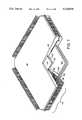
- FIG. 1is a cutaway perspective view of an integrated circuit package according to the invention.
- FIG. 2is a cross-sectional view of an integrated circuit assembly disposed in a mold cavity according to one embodiment of the invention.
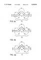
- FIG. 3ais a plan view of a portion of an individual lead with a stress relief section according to one embodiment of the invention.
- FIG. 3bis a plan view of a portion of an individual lead with a stress relief section according to another embodiment of the invention.
- FIG. 3cis a plan view of a portion of an individual lead with a stress relief section according to another embodiment of the invention.
- FIG. 3dis a plan view of a portion of an individual lead with a stress relief section according to another embodiment of the invention.
- FIG. 3eis a plan view of a portion of an individual lead with a stress relief section according to another embodiment of the invention.
- FIG. 4ais an orthogonal cross-sectional view of a heat sink with sealing ring according to one embodiment of the invention.
- FIG. 4bis an orthogonal cross-sectional view of a portion of a heat sink with sealing ring according to another embodiment of the invention.
- FIG. 4cis an orthogonal cross-sectional view of a portion of a heat sink with sealing ring according to yet another embodiment of the invention.
- FIG. 4dis an orthogonal cross-sectional view of a portion of a heat sink with sealing ring according to still another embodiment of the invention.
- FIG. 4eis an orthogonal cross-sectional view of a portion of a heat sink with a sealing ring according to another embodiment of the invention.
- FIG. 5is an orthogonal view of a heat sink with a treated surface according to an embodiment of the invention.
- FIG. 6ais a cross-sectional view of a prior art set of connections between a semiconductor die, leadframe die mounting paddle, and heat sink.
- FIG. 6bis a cross-sectional view of a set of connections between a semiconductor die, leadframe and heat sink according to one embodiment of the invention.
- FIG. 7ais a cross-sectional view of a heat sink connected to a lead by an adhesive-coated dielectric tape.
- FIG. 7bis a cross-sectional view of the connection of FIG. 7a showing electrical shorting that may result between heat sink and lead.
- FIG. 7cis a cross-sectional view of a heat sink connected to a lead by an adhesive-coated dielectric tape according to the invention.
- FIGS. 8a-8cshow successive steps in the formation of a sealing ring on a heat sink according to one embodiment of the invention.
- FIGS. 8d-8fshow successive steps in the formation of a shelf on a heat sink according to one embodiment of the invention.
- a package according to the inventionmay also be constructed with or without underlying or interactive interconnect circuitry composed of polymer laminate, ceramic, silicon or metal, or a mixture of these materials.
- FIG. 1shows a cutaway view of an integrated circuit package 100 according to the invention.
- a semiconductor die 101is mounted on a heat sink 102 by a suitable thermally conductive adhesive 110.
- a leadframe 103includes multiple leads 104 arranged in a generally radial manner around the circumference of the heat sink 102. (Note that though FIG. 1 shows a package with leads on all four sides, the invention is intended to encompass packages with leads on fewer than four sides as well.)
- the 103is attached to the heat sink 102 by an electrically insulative material 109.
- the leads 104have a stress relief section 108 located as shown in FIG. 1. Bond wires 105 connect the inner ends of each of the leads 104 to selected die contact pads 106.
- Encapsulant 107surrounds the heat sink 102, die 101, bond wires 105, and interior portions of the leads 104. Though not visible in FIG. 1, the side of the heat sink 102 to which the die 101 is not attached is exposed to the exterior of the encapsulate 107.
- the integrated circuit package 100 shown in FIG. 1is formed generally in the manner now to be described.
- the leadframe 103is attached to the outer periphery of the heat sink 102 with the adhesive material 109.
- the semiconductor die 101typically containing an integrated circuitry, is attached to the heat sink 102 with the thermally conductive adhesive 110.
- One end of a bond wire 105is attached to a selected die contact pad 106.
- the other end of the bond wire 105is attached to the inner end of one of the leads 104. This process is repeated for each of the bond wires 105.
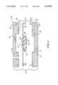
- FIG. 2shows a cross-sectional view of an integrated circuit 250 placed in a cavity 210 of a mold assembly 215. All elements described with respect to FIG. 1 retain the same numerical designation in FIG. 2. (Leads 104 are shown on only two sides of the heat sink 102 to increase the clarity of FIG. 2. In fact, leads 104 may be attached on all four sides of the heat sinks 102. For further clarity of FIG. 2, die contact pads 106 are also not shown.)
- the semiconductor die 101is attached to a surface 212 of the heat sink 102.
- An opposite surface 213 of the heat sink 102faces a surface 211 of the insert lower half 223 of the mold 215.
- the leads 104extend outside of the mold cavity 210. Select areas of the leadframe 103 (FIG. 1) are held in place by pins 218. Clamping of the leadframe 103 occurs in region 217 when the mold 215 is closed.
- the dimension 225(the combined thickness of heat sink 102 and electrically insulative material 109) is intentionally made slightly greater than the dimension 226 of the lower half 223 of the mold.
- the surface 213 of the heat sink 102contacts the surface 211 of the lower half 223 of the mold 215.
- the leads 104are raised slightly above the surface 220, prior to mold closure.
- the difference in the dimensions 225 and 226, and the raising of the leads 104 above the surface 220have been exaggerated in FIG. 2 for illustrative purposes.
- the two halves 222, 223 of the mold 215are brought together.
- the upper half 222 of the mold 215contacts the leads 104 at surface 221.
- the leads 104are forced down against the surface 220 of the lower mold half 223 as the mold 215 finishes closing, but are also held laterally in place by pins 218 inserted through corresponding holes 104a in the leadframe 103.
- leads 104are deflected slightly and tensile forces are induced in the leads 104 when the mold 215 is closed.
- the tensile forces in the leads 104act to press the heat sink surface 213 tightly against mold surface 211, thus assuring a good seal between heat sink surface 213 and mold surface 211.
- encapsulant 107is pressure fed (for instance, by transfer molding or injection molding) into the mold cavity 210 until the cavity 210 is full.
- One method of accomplishing the transfer of encapsulant 107known as top side gating, is shown in FIG. 2.
- Other gating methodssuch as gang pot, top plane gating, or bottom plane gating could also be utilized.
- Encapsulant 107is transferred through channel 230 in upper mold half 222 into the mold cavity 210.
- the mold 215is opened and the completed package 100 (FIG. 1) removed.
- the ends of the leads 104 left extending from the completed package 100may then be bent if, for instance, it is desired to have them form a quad-mounted package with extending contact pins as shown in FIG. 1.
- FIG. 3aA plan view of one embodiment of the stress relief zig-zag section 108 of a lead 104 is shown in FIG. 3a.
- the zig-zag section 108includes six angles ⁇ 1 , ⁇ 2 , ⁇ 3 , ⁇ 1 , ⁇ 2 , ⁇ 3 .
- a pair of anglesis formed (e.g., ⁇ 1 and ⁇ 1 ), one angle on each side of the lead 104.
- the "inner angle”is defined to be the angle of the pair that measures less than 180° (i.e., all of the ⁇ angles); the "outer angle” is the angle that measures more than 180° (i.e., all of the ⁇ angles).
- Such a zig-zag section 108has several benefits. First, it reduces contamination of the semiconductor die 101 by increasing the length of the path that contaminants must travel to enter the die area along the interface between a lead 104 and encapsulant 107. Second, it relieves tensile and compressive stresses experienced by the lead 104. When a tensile stress is created in the leads 104, the stress relief section 108 acts as a spring which relieves this stress, preventing the lead 104 from cracking, breaking or affecting the integrity of the lead-to-heat sink attachment. In the case of compressive forces, the stress relief section 108 works in an analogous way to prevent possible buckling of the lead 104.
- FIG. 3bshows a plan view of a stress relief section 108 in a lead 104 according to another embodiment of the invention.
- additional stress reliefis accomplished by rounding the vertices of the "inner angles" of each of the three bends in the lead 104. This rounding alleviates the stress concentration that builds up in the vicinity of the sharp-angled vertices of these angles in the lead 104.
- FIG. 3cshows a plan view of a stress relief section 108 in a lead 104 according to another embodiment of the invention.
- stress reliefis accomplished by rounding the vertices of all of the angles, both “inner angles” and “outer angles.” Again, the rounding alleviates stress concentration associated with sharp angles.
- FIGS. 3d and 3eshow additional embodiments of the stress relief section 108 according to the invention. Each of these embodiments is shown without rounding of either the “inner angles” or the “outer angles” of the bends of the leads 104. However, it should be noted that each of these embodiments could be formed with either or both of the "inner angles” or “outer angles” rounded as, for instance, shown in FIGS. 3b and 3c.
- FIG. 4ashows an orthogonal view of a heat sink 102 with an improved sealing ring 421a.
- the sealing ring 421aruns generally uninterrupted around the periphery of the heat sink 102 as shown in FIG. 4a (see also FIG. 1).
- a shelf 422is shown formed generally uninterrupted around the periphery of heat sink 102 at the interface of the surface 213 of the heat sink 102 and the surfaces 424 on which the sealing ring 421a is formed.
- the sealing ring 421ais formed by a cutting operation as shown in FIGS. 8a-8c.
- Cutting tools 850a, 850bcut down on the heat sink surfaces 212 and 213 at a predetermined distance from an edge of each of surfaces 212 and 213.
- the cutting tools 850a, 850bcut through the heat sink 102 to a predetermined depth.
- the cutting tools 850a, 850bdo not remove material from the heat sink 102; rather, the material which is cut by the cutting tools 850a, 850b is pushed toward the center of the heat sink 102 and away from the heat sink surface 424.
- FIG. 8bsuch an operation forms material around the periphery of the heat sink 102 into a "winged" or "keyed” shape. This residual material comprises the sealing ring 421a.
- a curved corner 422aAs shown by the dashed line in FIG. 4a, a second operation is performed on the heat sink 102. As shown in FIGS. 8d-8f, the curved corner 422a is squared off, preferably by stamping with a stamping tool 855, to form shelf 422. Other appropriate techniques can also be used to square off the curved corner 422a, such as, but not limited to, grinding and etching.
- FIGS. 4b-4dshow some other possible shapes of a according to the invention.
- FIG. 4bshows a sealing ring 421b with a Tshaped cross-section.
- FIG. 4cshows a sealing ring 421c that has a rectangular cross-section with dimples 425a, 425b formed on either side of the sealing ring 421c. Alternatively, dimples may be formed in only one side of the sealing ring 421c.
- sealing ring 421dshows a sealing ring 421d that has a rectangular cross-section with holes 426 extending through the sealing ring 421d.
- an indentation in heat sink 102forms sealing ring 421e.
- These other embodimentsare similar to the embodiment containing a "wing-shaped" sealing ring 421a in that they all provide a good compression seal between the sealing ring and the encapsulant 107 and they all reduce the migration of contaminants into the interior of the package 100.
- the various configurations of the sealing ringprovide two beneficial effects.
- these configurationsresult in the formation of a good compression seal between the sealing ring and the molded encapsulant 107.
- the formation of a compression sealis required because, otherwise, an inadequate bond is formed between the encapsulant 107 and heat sink 102.
- Without a good compression seal between the encapsulant 107 and heat sink 102trapped moisture can enter the interior of the package 100 and expand or pop interior surfaces away from the encapsulant 107.
- a good compression sealis created during solidification of the encapsulant 107 as it shrinks around and grips the sealing ring 421a. Without the sealing ring of the invention, the compressive forces of the encapsulant 107 form a weak seal against the heat sink 102 not capable of meeting package reliability requirements.
- the sealing ring, e.g., sealing ring, 421a of the inventionresults in a reduction of migration of contaminants to the area of the semiconductor die 101. This may occur in either of two ways.
- the improved compression seal formed between the heat sink 102 and the encapsulant 107reduces the gap between heat sink 102 and encapsulant 107 through which contaminants may potentially enter the interior of the package 100.
- the recessed shelf 422also provides two benefits. First, the rectangular path of the shelf 422 is longer than the curved corner 422a that would exist if the sealing ring were formed without the shelf 422. As with the sealing ring, this additional length of the interface between the heat sink 102 and the encapsulant 107 works to deter outside contaminants from entering the interior of the package 100 through the interface path.
- the creation of the recessed shelf 422provides a precisely defined sealing area at the heat sink interface which allows snug mating of the mold-to-heat sink 102 against the mold surface 211 during the molding process, thus preventing encapsulant flash or bleed on the exposed surface 213 of the heat sink 102. Too, the curved corner 422a that would exist if the shelf 422 were not formed provides more of a possibility that solidified encapsulant 107 will flake off at the surface interface between the heat sink 102 and encapsulant 107 after the package 100 has been completed.
- FIG. 5Another embodiment of the invention is shown in FIG. 5.
- the surface 424 of the heat sink 102is roughened by etching, sandblasting, rough plating, black oxide or other method. Roughened in this way, surface 424 provides a better bond between encapsulant 107 and heat sink 102 than if the surface 424 is not roughened. Further, the roughened surface 424 provides a lengthened interface between heat sink 102 and encapsulant 107 that helps reduce the influx of contaminants to the interior of the package 100.
- the leads 104may also be roughened in the same way to provide these benefits.
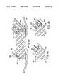
- FIG. 6ashows a cross-sectional view of a prior art set of connections between a semiconductor die 601, leadframe die mounting paddle 615, and heat sink 602.
- Semiconductor die 601 and heat sink 602are mounted on opposing sides of leadframe die mounting paddle 615.
- Thermally conductive adhesives 609 and 610are applied to paddle 615 surfaces contacting the heat sink 602 and die 601, respectively.
- Heatis transferred from the semiconductor die 601 through the first layer of adhesive 610 to the die mounting paddle 615.
- the heatleaves the packaged integrated circuit through the die mounting paddle support beams 604, or through the second layer of adhesive 609 and the heat sink 602.
- This configurationprovides inadequate heat transfer because of the inability of the die mounting paddle 615 to transmit sufficient heat to either the heat sink 602 or the die mounting paddle support beams 604, and because of the lack of an exposed surface of the heat sink 602.
- FIG. 6bis a cross-sectional view of a set of connections between a semiconductor die 101, leads 104 and heat sink 102 according to one embodiment of the invention.
- a thermally conductive adhesive 110attaches the semiconductor die 101 directly to the heat sink 102 and a dielectric adhesive material 109 attaches the leads 104 to the heat sink 102.
- the more direct connection between the die 101 and heat sink 102(as compared to the prior art connection shown in FIG. 6a) allows increased heat transfer from the die 101 to the heat sink 102.
- the heatis then, in turn, transferred outside of the package 100 (FIG. 1) through the surface of the heat sink 102 exposed outside the package 100.
- the exposed surfaceallows greater heat transfer from the package 100 than would occur if plastic encapsulant 107 (FIG. 1) covered the heat sink surface, because the presence of such encapsulant 107 represents an additional thermal barrier.
- greater heat transfer from the die 101 to the leads 104occurs because of the bonding of the leads 104 to the heat sink 102
- FIGS. 7a-7cshow another aspect of the invention.
- FIG. 7ashows a cross-sectional view of a heat sink 102 connected to a lead 104 by an adhesive coated dielectric tape 109.
- FIG. 7bshows if forces are applied to either the heat sink 102 or the outer ends of the leads 104, undesirable electrical shorting between the leads 104 and the heat sink 102 can result. Further, the possibility of such undesired electrical contact is exacerbated by manufacturing tolerances that allow variance in positioning of particular leads 104 with respect to the heat sink 102 and adhesive 109.
- FIG. 7cshows the connection of FIGS. 7a and 7b made according to one embodiment of the invention.
- the dielectric adhesive 109is affixed between the inner end 733 of the lead 104 and the periphery of the surface 732 of the heat sink 102.
- the adhesive 109is extended beyond the outer periphery of the heat sink 102, as well as beyond the inner end 733 of the lead 104, for distances sufficient to ensure electrical isolation between the leads 104 and the heat sink 102 even when mold closure bends the two toward each other.
- the greater area of the dielectric tape 109also reduces stress in the tape 109 that results from the transfer of forces between the heat sink 102 and leads 104, since those forces are distributed over a greater area.
Landscapes
- Engineering & Computer Science (AREA)
- Physics & Mathematics (AREA)
- Condensed Matter Physics & Semiconductors (AREA)
- General Physics & Mathematics (AREA)
- Computer Hardware Design (AREA)
- Microelectronics & Electronic Packaging (AREA)
- Power Engineering (AREA)
- Manufacturing & Machinery (AREA)
- Structures Or Materials For Encapsulating Or Coating Semiconductor Devices Or Solid State Devices (AREA)
- Lead Frames For Integrated Circuits (AREA)
- Cooling Or The Like Of Semiconductors Or Solid State Devices (AREA)
Abstract
Description
Claims (21)
Priority Applications (1)
| Application Number | Priority Date | Filing Date | Title |
|---|---|---|---|
| US07/973,354US5328870A (en) | 1992-01-17 | 1992-11-09 | Method for forming plastic molded package with heat sink for integrated circuit devices |
Applications Claiming Priority (2)
| Application Number | Priority Date | Filing Date | Title |
|---|---|---|---|
| US82229792A | 1992-01-17 | 1992-01-17 | |
| US07/973,354US5328870A (en) | 1992-01-17 | 1992-11-09 | Method for forming plastic molded package with heat sink for integrated circuit devices |
Related Parent Applications (1)
| Application Number | Title | Priority Date | Filing Date |
|---|---|---|---|
| US82229792ADivision | 1992-01-17 | 1992-01-17 |
Publications (1)
| Publication Number | Publication Date |
|---|---|
| US5328870Atrue US5328870A (en) | 1994-07-12 |
Family
ID=25235679
Family Applications (2)
| Application Number | Title | Priority Date | Filing Date |
|---|---|---|---|
| US07/973,354Expired - LifetimeUS5328870A (en) | 1992-01-17 | 1992-11-09 | Method for forming plastic molded package with heat sink for integrated circuit devices |
| US08/152,935Expired - LifetimeUS5455462A (en) | 1992-01-17 | 1993-11-15 | Plastic molded package with heat sink for integrated circuit devices |
Family Applications After (1)
| Application Number | Title | Priority Date | Filing Date |
|---|---|---|---|
| US08/152,935Expired - LifetimeUS5455462A (en) | 1992-01-17 | 1993-11-15 | Plastic molded package with heat sink for integrated circuit devices |
Country Status (2)
| Country | Link |
|---|---|
| US (2) | US5328870A (en) |
| JP (1) | JPH065746A (en) |
Cited By (34)
| Publication number | Priority date | Publication date | Assignee | Title |
|---|---|---|---|---|
| US5482898A (en)* | 1993-04-12 | 1996-01-09 | Amkor Electronics, Inc. | Method for forming a semiconductor device having a thermal dissipator and electromagnetic shielding |
| US5530278A (en)* | 1995-04-24 | 1996-06-25 | Xerox Corporation | Semiconductor chip having a dam to prevent contamination of photosensitive structures thereon |
| WO1996027903A1 (en)* | 1995-03-06 | 1996-09-12 | National Semiconductor Corporation | Heat sink for integrated circuit packages |
| US5594282A (en)* | 1993-12-16 | 1997-01-14 | Seiko Epson Corporation | Resin sealing type semiconductor device and method of making the same |
| US5609889A (en)* | 1995-05-26 | 1997-03-11 | Hestia Technologies, Inc. | Apparatus for encapsulating electronic packages |
| US5633529A (en)* | 1994-07-13 | 1997-05-27 | Seiko Epson Corporation | Resin sealing type semiconductor device and method of making the same |
| US5650593A (en)* | 1994-05-26 | 1997-07-22 | Amkor Electronics, Inc. | Thermally enhanced chip carrier package |
| US5652463A (en)* | 1995-05-26 | 1997-07-29 | Hestia Technologies, Inc. | Transfer modlded electronic package having a passage means |
| US5652461A (en)* | 1992-06-03 | 1997-07-29 | Seiko Epson Corporation | Semiconductor device with a convex heat sink |
| EP0732744A3 (en)* | 1995-03-17 | 1997-08-27 | Seiko Epson Corp | Semiconductive device of the resin encapsulation type and manufacturing method |
| US5686361A (en)* | 1992-06-03 | 1997-11-11 | Seiko Epson Corporation | Method for manufacturing a semiconductor device having a heat radiator |
| US5719442A (en)* | 1994-11-11 | 1998-02-17 | Seiko Epson Corporation | Resin sealing type semiconductor device |
| US5787569A (en)* | 1996-02-21 | 1998-08-04 | Lucent Technologies Inc. | Encapsulated package for power magnetic devices and method of manufacture therefor |
| US5801435A (en)* | 1995-02-27 | 1998-09-01 | Seiko Epson Corporation | Resin sealing type semiconductor device and method of making the same |
| US5827999A (en)* | 1994-05-26 | 1998-10-27 | Amkor Electronics, Inc. | Homogeneous chip carrier package |
| US6105846A (en)* | 1998-04-02 | 2000-08-22 | Micron Technology, Inc. | Non-conductive and self-leveling leadframe clamp insert for wirebonding integrated circuits |
| US6258629B1 (en) | 1999-08-09 | 2001-07-10 | Amkor Technology, Inc. | Electronic device package and leadframe and method for making the package |
| US6429513B1 (en) | 2001-05-25 | 2002-08-06 | Amkor Technology, Inc. | Active heat sink for cooling a semiconductor chip |
| US6562655B1 (en) | 2001-04-20 | 2003-05-13 | Amkor Technology, Inc. | Heat spreader with spring IC package fabrication method |
| US6566164B1 (en) | 2000-12-07 | 2003-05-20 | Amkor Technology, Inc. | Exposed copper strap in a semiconductor package |
| US6580167B1 (en) | 2001-04-20 | 2003-06-17 | Amkor Technology, Inc. | Heat spreader with spring IC package |
| US6614100B1 (en)* | 1996-06-24 | 2003-09-02 | Infineon Technologies Ag | Lead frame for the installation of an integrated circuit in an injection-molded package |
| US6634538B2 (en) | 1998-04-02 | 2003-10-21 | Micron Technology, Inc. | Non-conductive and self-leveling leadframe clamp insert for wirebonding integrated circuits |
| US6660559B1 (en) | 2001-06-25 | 2003-12-09 | Amkor Technology, Inc. | Method of making a chip carrier package using laser ablation |
| US6696750B1 (en) | 2003-01-10 | 2004-02-24 | Siliconware Precision Industries Co., Ltd. | Semiconductor package with heat dissipating structure |
| US20040053447A1 (en)* | 2001-06-29 | 2004-03-18 | Foster Donald Craig | Leadframe having fine pitch bond fingers formed using laser cutting method |
| US6919631B1 (en) | 2001-12-07 | 2005-07-19 | Amkor Technology, Inc. | Structures for improving heat dissipation in stacked semiconductor packages |
| US20050186711A1 (en)* | 2004-02-20 | 2005-08-25 | Yee Richard M.L. | Mould for encapsulating a leadframe package and method of making the same |
| US7126218B1 (en) | 2001-08-07 | 2006-10-24 | Amkor Technology, Inc. | Embedded heat spreader ball grid array |
| US20060267184A1 (en)* | 1997-07-02 | 2006-11-30 | Kinsman Larry D | Varied-thickness heat sink for integrated circuit (IC) package |
| US20090140403A1 (en)* | 2007-11-30 | 2009-06-04 | Infineon Technologies Ag | Electronic device |
| US7560309B1 (en) | 2005-07-26 | 2009-07-14 | Marvell International Ltd. | Drop-in heat sink and exposed die-back for molded flip die package |
| WO2012025448A1 (en)* | 2010-08-25 | 2012-03-01 | Robert Bosch Gmbh | Electrical circuit having circuit components to be cooled, heat sink, and method for sealingly embedding an electrical circuit |
| CN111615747A (en)* | 2017-12-27 | 2020-09-01 | 三菱电机株式会社 | semiconductor device |
Families Citing this family (18)
| Publication number | Priority date | Publication date | Assignee | Title |
|---|---|---|---|---|
| US5798570A (en)* | 1996-06-28 | 1998-08-25 | Kabushiki Kaisha Gotoh Seisakusho | Plastic molded semiconductor package with thermal dissipation means |
| US5977622A (en)* | 1997-04-25 | 1999-11-02 | Lsi Logic Corporation | Stiffener with slots for clip-on heat sink attachment |
| US5898571A (en)* | 1997-04-28 | 1999-04-27 | Lsi Logic Corporation | Apparatus and method for clip-on attachment of heat sinks to encapsulated semiconductor packages |
| US6011304A (en)* | 1997-05-05 | 2000-01-04 | Lsi Logic Corporation | Stiffener ring attachment with holes and removable snap-in heat sink or heat spreader/lid |
| US6072230A (en)* | 1997-09-09 | 2000-06-06 | Texas Instruments Incorporated | Exposed leadframe for semiconductor packages and bend forming method of fabrication |
| US6337228B1 (en) | 1999-05-12 | 2002-01-08 | Amkor Technology, Inc. | Low-cost printed circuit board with integral heat sink for semiconductor package |
| TW510158B (en)* | 1999-05-14 | 2002-11-11 | Siliconware Precision Industries Co Ltd | Heat dissipation structure for semiconductor device |
| JP3277996B2 (en)* | 1999-06-07 | 2002-04-22 | 日本電気株式会社 | Circuit device and method of manufacturing the same |
| US6900508B2 (en) | 2002-04-16 | 2005-05-31 | Stmicroelectronics, Inc. | Embedded flat film molding |
| DE10345247B4 (en)* | 2003-09-29 | 2007-10-04 | Infineon Technologies Ag | Use of conductor tracks as Krallkörper |
| US7361985B2 (en)* | 2004-10-27 | 2008-04-22 | Freescale Semiconductor, Inc. | Thermally enhanced molded package for semiconductors |
| US7732848B2 (en)* | 2007-05-31 | 2010-06-08 | Infineon Technologies Ag | Power semiconductor device with improved heat dissipation |
| US9532459B2 (en)* | 2013-08-12 | 2016-12-27 | Infineon Technologies Ag | Electronic module and method of manufacturing the same |
| US9554488B2 (en)* | 2014-04-18 | 2017-01-24 | Raytheon Company | Method to align surface mount packages for thermal enhancement |
| JP6217884B2 (en)* | 2015-09-29 | 2017-10-25 | 三菱電機株式会社 | Semiconductor device and manufacturing method thereof |
| JP6498829B1 (en)* | 2018-09-19 | 2019-04-10 | 株式会社加藤電器製作所 | Semiconductor module |
| US12009803B2 (en) | 2019-04-04 | 2024-06-11 | Ningbo Semiconductor International Corporation | Bulk acoustic wave resonator, filter and radio frequency communication system |
| CN111786651A (en)* | 2019-04-04 | 2020-10-16 | 中芯集成电路(宁波)有限公司上海分公司 | Bulk acoustic wave resonator, method of manufacturing the same, filter, and radio frequency communication system |
Citations (35)
| Publication number | Priority date | Publication date | Assignee | Title |
|---|---|---|---|---|
| US3564352A (en)* | 1968-12-30 | 1971-02-16 | Fairchild Camera Instr Co | Strip design for a low cost plastic transistor |
| US3838984A (en)* | 1973-04-16 | 1974-10-01 | Sperry Rand Corp | Flexible carrier and interconnect for uncased ic chips |
| US4074342A (en)* | 1974-12-20 | 1978-02-14 | International Business Machines Corporation | Electrical package for lsi devices and assembly process therefor |
| US4105861A (en)* | 1975-09-29 | 1978-08-08 | Semi-Alloys, Inc. | Hermetically sealed container for semiconductor and other electronic devices |
| US4168507A (en)* | 1977-11-21 | 1979-09-18 | Motorola, Inc. | Structure and technique for achieving reduced inductive effect of undesired components of common lead inductance in a semiconductive RF power package |
| JPS5745959A (en)* | 1980-09-02 | 1982-03-16 | Nec Corp | Resin-sealed semiconductor device |
| US4410927A (en)* | 1982-01-21 | 1983-10-18 | Olin Corporation | Casing for an electrical component having improved strength and heat transfer characteristics |
| US4461924A (en)* | 1982-01-21 | 1984-07-24 | Olin Corporation | Semiconductor casing |
| US4480262A (en)* | 1982-07-15 | 1984-10-30 | Olin Corporation | Semiconductor casing |
| JPS6139555A (en)* | 1984-07-31 | 1986-02-25 | Toshiba Corp | Resin sealed type semiconductor device with heat sink |
| US4594770A (en)* | 1982-07-15 | 1986-06-17 | Olin Corporation | Method of making semiconductor casing |
| US4680613A (en)* | 1983-12-01 | 1987-07-14 | Fairchild Semiconductor Corporation | Low impedance package for integrated circuit die |
| US4701999A (en)* | 1985-12-17 | 1987-10-27 | Pnc, Inc. | Method of making sealed housings containing delicate structures |
| US4737395A (en)* | 1983-11-29 | 1988-04-12 | Ibiden Co. Ltd. | Printed wiring board for mounting electronic parts and process for producing the same |
| JPS63205935A (en)* | 1987-02-23 | 1988-08-25 | Toshiba Corp | Resin-encapsulated semiconductor device with heat sink |
| US4769344A (en)* | 1984-06-04 | 1988-09-06 | Mitsubishi Denki Kabushiki Kaisha | Method of resin encapsulating a semiconductor device |
| JPS63233555A (en)* | 1987-03-23 | 1988-09-29 | Toshiba Corp | Resin-encapsulated semiconductor device |
| JPS6447058A (en)* | 1987-08-18 | 1989-02-21 | Shinko Electric Ind Co | Package for semiconductor device |
| US4835120A (en)* | 1987-01-12 | 1989-05-30 | Debendra Mallik | Method of making a multilayer molded plastic IC package |
| JPH01146346A (en)* | 1987-12-02 | 1989-06-08 | Nec Corp | Integrated circuit package |
| US4872047A (en)* | 1986-11-07 | 1989-10-03 | Olin Corporation | Semiconductor die attach system |
| US4888449A (en)* | 1988-01-04 | 1989-12-19 | Olin Corporation | Semiconductor package |
| US4890152A (en)* | 1986-02-14 | 1989-12-26 | Matsushita Electric Works, Ltd. | Plastic molded chip carrier package and method of fabricating the same |
| US4891687A (en)* | 1987-01-12 | 1990-01-02 | Intel Corporation | Multi-layer molded plastic IC package |
| US4943844A (en)* | 1985-11-22 | 1990-07-24 | Texas Instruments Incorporated | High-density package |
| US4949220A (en)* | 1988-02-24 | 1990-08-14 | Nec Corporation | Hybrid IC with heat sink |
| US4974057A (en)* | 1986-10-31 | 1990-11-27 | Texas Instruments Incorporated | Semiconductor device package with circuit board and resin |
| US4975761A (en)* | 1989-09-05 | 1990-12-04 | Advanced Micro Devices, Inc. | High performance plastic encapsulated package for integrated circuit die |
| US4994936A (en)* | 1990-02-12 | 1991-02-19 | Rogers Corporation | Molded integrated circuit package incorporating decoupling capacitor |
| US4994897A (en)* | 1989-10-26 | 1991-02-19 | Motorola, Inc. | Multi-level semiconductor package |
| US5041902A (en)* | 1989-12-14 | 1991-08-20 | Motorola, Inc. | Molded electronic package with compression structures |
| JPH043450A (en)* | 1990-04-19 | 1992-01-08 | Mitsubishi Electric Corp | Resin-encapsulated semiconductor device |
| US5102828A (en)* | 1983-03-09 | 1992-04-07 | Sgs-Ates Componenti Elettronici S.P.A. | Method for manufacturing a semiconductor card with electrical contacts on both faces |
| US5172214A (en)* | 1991-02-06 | 1992-12-15 | Motorola, Inc. | Leadless semiconductor device and method for making the same |
| US5202288A (en)* | 1990-06-01 | 1993-04-13 | Robert Bosch Gmbh | Method of manufacturing an electronic circuit component incorporating a heat sink |
- 1992
- 1992-11-09USUS07/973,354patent/US5328870A/ennot_activeExpired - Lifetime
- 1993
- 1993-01-08JPJP5001975Apatent/JPH065746A/enactivePending
- 1993-11-15USUS08/152,935patent/US5455462A/ennot_activeExpired - Lifetime
Patent Citations (36)
| Publication number | Priority date | Publication date | Assignee | Title |
|---|---|---|---|---|
| US3564352A (en)* | 1968-12-30 | 1971-02-16 | Fairchild Camera Instr Co | Strip design for a low cost plastic transistor |
| US3838984A (en)* | 1973-04-16 | 1974-10-01 | Sperry Rand Corp | Flexible carrier and interconnect for uncased ic chips |
| US4074342A (en)* | 1974-12-20 | 1978-02-14 | International Business Machines Corporation | Electrical package for lsi devices and assembly process therefor |
| US4105861A (en)* | 1975-09-29 | 1978-08-08 | Semi-Alloys, Inc. | Hermetically sealed container for semiconductor and other electronic devices |
| US4168507A (en)* | 1977-11-21 | 1979-09-18 | Motorola, Inc. | Structure and technique for achieving reduced inductive effect of undesired components of common lead inductance in a semiconductive RF power package |
| JPS5745959A (en)* | 1980-09-02 | 1982-03-16 | Nec Corp | Resin-sealed semiconductor device |
| US4410927A (en)* | 1982-01-21 | 1983-10-18 | Olin Corporation | Casing for an electrical component having improved strength and heat transfer characteristics |
| US4461924A (en)* | 1982-01-21 | 1984-07-24 | Olin Corporation | Semiconductor casing |
| US4480262A (en)* | 1982-07-15 | 1984-10-30 | Olin Corporation | Semiconductor casing |
| US4594770A (en)* | 1982-07-15 | 1986-06-17 | Olin Corporation | Method of making semiconductor casing |
| US5102828A (en)* | 1983-03-09 | 1992-04-07 | Sgs-Ates Componenti Elettronici S.P.A. | Method for manufacturing a semiconductor card with electrical contacts on both faces |
| US4737395A (en)* | 1983-11-29 | 1988-04-12 | Ibiden Co. Ltd. | Printed wiring board for mounting electronic parts and process for producing the same |
| US4773955A (en)* | 1983-11-29 | 1988-09-27 | Ibiden Co. Ltd. | Printed wiring board for mounting electronic parts and process for producing the same |
| US4680613A (en)* | 1983-12-01 | 1987-07-14 | Fairchild Semiconductor Corporation | Low impedance package for integrated circuit die |
| US4769344A (en)* | 1984-06-04 | 1988-09-06 | Mitsubishi Denki Kabushiki Kaisha | Method of resin encapsulating a semiconductor device |
| JPS6139555A (en)* | 1984-07-31 | 1986-02-25 | Toshiba Corp | Resin sealed type semiconductor device with heat sink |
| US4943844A (en)* | 1985-11-22 | 1990-07-24 | Texas Instruments Incorporated | High-density package |
| US4701999A (en)* | 1985-12-17 | 1987-10-27 | Pnc, Inc. | Method of making sealed housings containing delicate structures |
| US4890152A (en)* | 1986-02-14 | 1989-12-26 | Matsushita Electric Works, Ltd. | Plastic molded chip carrier package and method of fabricating the same |
| US4974057A (en)* | 1986-10-31 | 1990-11-27 | Texas Instruments Incorporated | Semiconductor device package with circuit board and resin |
| US4872047A (en)* | 1986-11-07 | 1989-10-03 | Olin Corporation | Semiconductor die attach system |
| US4835120A (en)* | 1987-01-12 | 1989-05-30 | Debendra Mallik | Method of making a multilayer molded plastic IC package |
| US4891687A (en)* | 1987-01-12 | 1990-01-02 | Intel Corporation | Multi-layer molded plastic IC package |
| JPS63205935A (en)* | 1987-02-23 | 1988-08-25 | Toshiba Corp | Resin-encapsulated semiconductor device with heat sink |
| JPS63233555A (en)* | 1987-03-23 | 1988-09-29 | Toshiba Corp | Resin-encapsulated semiconductor device |
| JPS6447058A (en)* | 1987-08-18 | 1989-02-21 | Shinko Electric Ind Co | Package for semiconductor device |
| JPH01146346A (en)* | 1987-12-02 | 1989-06-08 | Nec Corp | Integrated circuit package |
| US4888449A (en)* | 1988-01-04 | 1989-12-19 | Olin Corporation | Semiconductor package |
| US4949220A (en)* | 1988-02-24 | 1990-08-14 | Nec Corporation | Hybrid IC with heat sink |
| US4975761A (en)* | 1989-09-05 | 1990-12-04 | Advanced Micro Devices, Inc. | High performance plastic encapsulated package for integrated circuit die |
| US4994897A (en)* | 1989-10-26 | 1991-02-19 | Motorola, Inc. | Multi-level semiconductor package |
| US5041902A (en)* | 1989-12-14 | 1991-08-20 | Motorola, Inc. | Molded electronic package with compression structures |
| US4994936A (en)* | 1990-02-12 | 1991-02-19 | Rogers Corporation | Molded integrated circuit package incorporating decoupling capacitor |
| JPH043450A (en)* | 1990-04-19 | 1992-01-08 | Mitsubishi Electric Corp | Resin-encapsulated semiconductor device |
| US5202288A (en)* | 1990-06-01 | 1993-04-13 | Robert Bosch Gmbh | Method of manufacturing an electronic circuit component incorporating a heat sink |
| US5172214A (en)* | 1991-02-06 | 1992-12-15 | Motorola, Inc. | Leadless semiconductor device and method for making the same |
Cited By (51)
| Publication number | Priority date | Publication date | Assignee | Title |
|---|---|---|---|---|
| US5652461A (en)* | 1992-06-03 | 1997-07-29 | Seiko Epson Corporation | Semiconductor device with a convex heat sink |
| US5653891A (en)* | 1992-06-03 | 1997-08-05 | Seiko Epson Corporation | Method of producing a semiconductor device with a heat sink |
| US5686361A (en)* | 1992-06-03 | 1997-11-11 | Seiko Epson Corporation | Method for manufacturing a semiconductor device having a heat radiator |
| US5482898A (en)* | 1993-04-12 | 1996-01-09 | Amkor Electronics, Inc. | Method for forming a semiconductor device having a thermal dissipator and electromagnetic shielding |
| US5891759A (en)* | 1993-12-16 | 1999-04-06 | Seiko Epson Corporation | Method of making a multiple heat sink resin sealing type semiconductor device |
| US5594282A (en)* | 1993-12-16 | 1997-01-14 | Seiko Epson Corporation | Resin sealing type semiconductor device and method of making the same |
| US5827999A (en)* | 1994-05-26 | 1998-10-27 | Amkor Electronics, Inc. | Homogeneous chip carrier package |
| US5650593A (en)* | 1994-05-26 | 1997-07-22 | Amkor Electronics, Inc. | Thermally enhanced chip carrier package |
| US5633529A (en)* | 1994-07-13 | 1997-05-27 | Seiko Epson Corporation | Resin sealing type semiconductor device and method of making the same |
| US5719442A (en)* | 1994-11-11 | 1998-02-17 | Seiko Epson Corporation | Resin sealing type semiconductor device |
| US5801435A (en)* | 1995-02-27 | 1998-09-01 | Seiko Epson Corporation | Resin sealing type semiconductor device and method of making the same |
| WO1996027903A1 (en)* | 1995-03-06 | 1996-09-12 | National Semiconductor Corporation | Heat sink for integrated circuit packages |
| EP0732744A3 (en)* | 1995-03-17 | 1997-08-27 | Seiko Epson Corp | Semiconductive device of the resin encapsulation type and manufacturing method |
| US5777380A (en)* | 1995-03-17 | 1998-07-07 | Seiko Epson Corporation | Resin sealing type semiconductor device having thin portions formed on the leads |
| US5530278A (en)* | 1995-04-24 | 1996-06-25 | Xerox Corporation | Semiconductor chip having a dam to prevent contamination of photosensitive structures thereon |
| US5766986A (en)* | 1995-05-26 | 1998-06-16 | Hestia Technologies, Inc. | Method of transfer molding electronic packages and packages produced thereby |
| US5776512A (en)* | 1995-05-26 | 1998-07-07 | Hestia Technologies, Inc. | Apparatus for encapsulating electronic packages |
| US5652463A (en)* | 1995-05-26 | 1997-07-29 | Hestia Technologies, Inc. | Transfer modlded electronic package having a passage means |
| US5609889A (en)* | 1995-05-26 | 1997-03-11 | Hestia Technologies, Inc. | Apparatus for encapsulating electronic packages |
| US5787569A (en)* | 1996-02-21 | 1998-08-04 | Lucent Technologies Inc. | Encapsulated package for power magnetic devices and method of manufacture therefor |
| US6614100B1 (en)* | 1996-06-24 | 2003-09-02 | Infineon Technologies Ag | Lead frame for the installation of an integrated circuit in an injection-molded package |
| US20060267184A1 (en)* | 1997-07-02 | 2006-11-30 | Kinsman Larry D | Varied-thickness heat sink for integrated circuit (IC) package |
| US6375061B1 (en) | 1998-04-02 | 2002-04-23 | Micron Technology, Inc. | Non-conductive and self-leveling leadframe clamp insert for wirebonding integrated circuits |
| US6634538B2 (en) | 1998-04-02 | 2003-10-21 | Micron Technology, Inc. | Non-conductive and self-leveling leadframe clamp insert for wirebonding integrated circuits |
| US6352191B1 (en) | 1998-04-02 | 2002-03-05 | Micron Technology, Inc. | Non-conductive and self-leveling leadframe clamp insert for wirebonding integrated circuits |
| US6105846A (en)* | 1998-04-02 | 2000-08-22 | Micron Technology, Inc. | Non-conductive and self-leveling leadframe clamp insert for wirebonding integrated circuits |
| US6921017B2 (en) | 1998-04-02 | 2005-07-26 | Micron Technology, Inc. | Non-conductive and self-leveling leadframe clamp insert for wirebonding integrated circuits |
| US20040026486A1 (en)* | 1998-04-02 | 2004-02-12 | Sven Evers | Non-conductive and self-leveling leadframe clamp insert for wirebonding integrated circuits |
| US6588649B2 (en) | 1998-04-02 | 2003-07-08 | Micron Technology, Inc. | Non-conductive and self-leveling leadframe clamp insert for wirebonding integrated circuits |
| US6138891A (en)* | 1998-04-02 | 2000-10-31 | Micron Technology, Inc. | Non-conductive and self-leveling leadframe clamp insert for wirebonding integrated circuits |
| US6258629B1 (en) | 1999-08-09 | 2001-07-10 | Amkor Technology, Inc. | Electronic device package and leadframe and method for making the package |
| US6339252B1 (en) | 1999-08-09 | 2002-01-15 | Amkor Technology, Inc. | Electronic device package and leadframe |
| US6723582B2 (en) | 2000-12-07 | 2004-04-20 | Amkor Technology, Inc. | Method of making a semiconductor package having exposed metal strap |
| US6566164B1 (en) | 2000-12-07 | 2003-05-20 | Amkor Technology, Inc. | Exposed copper strap in a semiconductor package |
| US6562655B1 (en) | 2001-04-20 | 2003-05-13 | Amkor Technology, Inc. | Heat spreader with spring IC package fabrication method |
| US6580167B1 (en) | 2001-04-20 | 2003-06-17 | Amkor Technology, Inc. | Heat spreader with spring IC package |
| US6429513B1 (en) | 2001-05-25 | 2002-08-06 | Amkor Technology, Inc. | Active heat sink for cooling a semiconductor chip |
| US6660559B1 (en) | 2001-06-25 | 2003-12-09 | Amkor Technology, Inc. | Method of making a chip carrier package using laser ablation |
| US20040053447A1 (en)* | 2001-06-29 | 2004-03-18 | Foster Donald Craig | Leadframe having fine pitch bond fingers formed using laser cutting method |
| US7126218B1 (en) | 2001-08-07 | 2006-10-24 | Amkor Technology, Inc. | Embedded heat spreader ball grid array |
| US6919631B1 (en) | 2001-12-07 | 2005-07-19 | Amkor Technology, Inc. | Structures for improving heat dissipation in stacked semiconductor packages |
| US6696750B1 (en) | 2003-01-10 | 2004-02-24 | Siliconware Precision Industries Co., Ltd. | Semiconductor package with heat dissipating structure |
| US20050186711A1 (en)* | 2004-02-20 | 2005-08-25 | Yee Richard M.L. | Mould for encapsulating a leadframe package and method of making the same |
| US7351611B2 (en) | 2004-02-20 | 2008-04-01 | Carsem (M) Sdn Bhd | Method of making the mould for encapsulating a leadframe package |
| US7560309B1 (en) | 2005-07-26 | 2009-07-14 | Marvell International Ltd. | Drop-in heat sink and exposed die-back for molded flip die package |
| US20090140403A1 (en)* | 2007-11-30 | 2009-06-04 | Infineon Technologies Ag | Electronic device |
| US8030742B2 (en) | 2007-11-30 | 2011-10-04 | Infineon Technologies | Electronic device having profiled elements extending from planar surfaces |
| WO2012025448A1 (en)* | 2010-08-25 | 2012-03-01 | Robert Bosch Gmbh | Electrical circuit having circuit components to be cooled, heat sink, and method for sealingly embedding an electrical circuit |
| CN103069567A (en)* | 2010-08-25 | 2013-04-24 | 罗伯特·博世有限公司 | Electrical circuit having circuit components to be cooled, heat sink, and method for sealingly embedding an electrical circuit |
| CN111615747A (en)* | 2017-12-27 | 2020-09-01 | 三菱电机株式会社 | semiconductor device |
| CN111615747B (en)* | 2017-12-27 | 2023-10-03 | 三菱电机株式会社 | Semiconductor device with a semiconductor device having a plurality of semiconductor chips |
Also Published As
| Publication number | Publication date |
|---|---|
| US5455462A (en) | 1995-10-03 |
| JPH065746A (en) | 1994-01-14 |
Similar Documents
| Publication | Publication Date | Title |
|---|---|---|
| US5328870A (en) | Method for forming plastic molded package with heat sink for integrated circuit devices | |
| US5278446A (en) | Reduced stress plastic package | |
| US5381042A (en) | Packaged integrated circuit including heat slug having an exposed surface | |
| US5147821A (en) | Method for making a thermally enhanced semiconductor device by holding a leadframe against a heatsink through vacuum suction in a molding operation | |
| KR100396130B1 (en) | Semiconductor device | |
| US5214846A (en) | Packaging of semiconductor chips | |
| US5953593A (en) | Method and mold for manufacturing a plastic package for an electronic device having a heat sink | |
| JP2540478B2 (en) | Heat sink for semiconductor device and manufacturing method thereof | |
| US4910581A (en) | Internally molded isolated package | |
| JPH0851168A (en) | Bga package and molding die used for manufacture bga package | |
| JPH088375A (en) | Semiconductor device and lead frame and mold used for manufacturing the same | |
| KR970010672B1 (en) | Method for forming plastic mold package with a heat sink for integrated circuit apparatus | |
| JP3688440B2 (en) | Semiconductor device | |
| KR970010671B1 (en) | Plastic mold package with heat sink for integrated circuit device | |
| US20240379474A1 (en) | A packaged semiconductor device and method of manufacturing the same | |
| JP3747991B2 (en) | Manufacturing method of semiconductor device | |
| KR0152574B1 (en) | Lead frame with stepped die pad portion | |
| JPH09129661A (en) | Molding apparatus and molding method | |
| JPH09153506A (en) | Mold for semiconductor resin encapsulation and method for manufacturing semiconductor device using the same | |
| JP2802966B2 (en) | Method for manufacturing resin-encapsulated electronic component | |
| JPH04277660A (en) | Integrated circuit package | |
| JP2602234B2 (en) | Resin-sealed semiconductor device | |
| JPS6020546A (en) | semiconductor equipment | |
| JP2997182B2 (en) | Resin encapsulated semiconductor device for surface mounting | |
| JPH05291349A (en) | A flexible base material for mounting a semiconductor chip and a mold used for resin sealing of a semiconductor mounted on the flexible base material. |
Legal Events
| Date | Code | Title | Description |
|---|---|---|---|
| STCF | Information on status: patent grant | Free format text:PATENTED CASE | |
| CC | Certificate of correction | ||
| FPAY | Fee payment | Year of fee payment:4 | |
| AS | Assignment | Owner name:GUARDIAN ASSETS, INC., PENNSYLVANIA Free format text:SECURITY INTEREST;ASSIGNOR:AMKOR TECHNOLOGY, INC.;REEL/FRAME:011122/0773 Effective date:20000428 | |
| AS | Assignment | Owner name:SOCIETE GENERALE, NEW YORK Free format text:RE-RECORD TO CORRECT RECEIVING PARTY NAME ON A DOCUMENT PREVIOUSLY RECORDED ON REEL 011122, FRAME 0773.;ASSIGNORS:AMKOR TECHNOLOGY, INC.;GUARDIAN ASSETS, INC.;REEL/FRAME:011457/0702 Effective date:20000428 | |
| AS | Assignment | Owner name:CITICORP USA, INC., NEW YORK Free format text:SECURITY INTEREST;ASSIGNORS:SOCIETE GENERALE;GUARDIAN ASSETS, INC.;REEL/FRAME:011682/0416 Effective date:20010330 | |
| FPAY | Fee payment | Year of fee payment:8 | |
| AS | Assignment | Owner name:CITICORP NORTH AMERICA, INC. AS ADMINISTRATIVE AGE Free format text:SECURITY AGREEMENT;ASSIGNORS:AMKOR TECHNOLOGY, INC.;GUARDIAN ASSETS, INC.;REEL/FRAME:014885/0691 Effective date:20040629 | |
| AS | Assignment | Owner name:AMKOR TECHNOLOGY, INC., PENNSYLVANIA Free format text:RELEASE OF LIEN ON PATENTS;ASSIGNOR:CITICORP USA, INC. AS COLLATERAL AGENT;REEL/FRAME:015603/0572 Effective date:20040629 | |
| AS | Assignment | Owner name:CITICORP NORTH AMERICA, INC. AS "AGENT", NEW YORK Free format text:SECURITY AGREEMENT;ASSIGNORS:AMKOR TECHNOLOGY, INC.;GUARDIAN ASSETS, INC.;REEL/FRAME:015942/0521 Effective date:20041027 | |
| FEPP | Fee payment procedure | Free format text:PAYOR NUMBER ASSIGNED (ORIGINAL EVENT CODE: ASPN); ENTITY STATUS OF PATENT OWNER: LARGE ENTITY | |
| AS | Assignment | Owner name:BANK OF AMERICA, N.A., TEXAS Free format text:SECURITY AGREEMENT;ASSIGNOR:AMKOR TECHNOLOGY, INC.;REEL/FRAME:017379/0630 Effective date:20051123 Owner name:AMKOR TECHNOLOGY, INC., ARIZONA Free format text:TERMINATION & RELEASE OF PATENT SECURITY AGREEMENT;ASSIGNOR:CITICORP NORTH AMERICA, INC.;REEL/FRAME:017388/0868 Effective date:20051128 | |
| FPAY | Fee payment | Year of fee payment:12 | |
| AS | Assignment | Owner name:BANK OF AMERICA, N.A., AS AGENT, CALIFORNIA Free format text:SECURITY INTEREST;ASSIGNOR:AMKOR TECHNOLOGY, INC.;REEL/FRAME:046683/0139 Effective date:20180713 | |
| AS | Assignment | Owner name:AMKOR TECHNOLOGY SINGAPORE HOLDING PTE.LTD., SINGAPORE Free format text:ASSIGNMENT OF ASSIGNORS INTEREST;ASSIGNOR:AMKOR TECHNOLOGY, INC.;REEL/FRAME:054036/0599 Effective date:20191119 |