US5327009A - Miniaturized integrated circuit package - Google Patents
Miniaturized integrated circuit packageDownload PDFInfo
- Publication number
- US5327009A US5327009AUS08/064,980US6498093AUS5327009AUS 5327009 AUS5327009 AUS 5327009AUS 6498093 AUS6498093 AUS 6498093AUS 5327009 AUS5327009 AUS 5327009A
- Authority
- US
- United States
- Prior art keywords
- chip
- terminals
- inner end
- semiconductor chip
- lead fingers
- Prior art date
- Legal status (The legal status is an assumption and is not a legal conclusion. Google has not performed a legal analysis and makes no representation as to the accuracy of the status listed.)
- Expired - Lifetime
Links
Images

Classifications
- H—ELECTRICITY
- H01—ELECTRIC ELEMENTS
- H01L—SEMICONDUCTOR DEVICES NOT COVERED BY CLASS H10
- H01L24/00—Arrangements for connecting or disconnecting semiconductor or solid-state bodies; Methods or apparatus related thereto
- H01L24/01—Means for bonding being attached to, or being formed on, the surface to be connected, e.g. chip-to-package, die-attach, "first-level" interconnects; Manufacturing methods related thereto
- H01L24/02—Bonding areas ; Manufacturing methods related thereto
- H01L24/04—Structure, shape, material or disposition of the bonding areas prior to the connecting process
- H01L24/05—Structure, shape, material or disposition of the bonding areas prior to the connecting process of an individual bonding area
- H—ELECTRICITY
- H01—ELECTRIC ELEMENTS
- H01L—SEMICONDUCTOR DEVICES NOT COVERED BY CLASS H10
- H01L23/00—Details of semiconductor or other solid state devices
- H01L23/48—Arrangements for conducting electric current to or from the solid state body in operation, e.g. leads, terminal arrangements ; Selection of materials therefor
- H01L23/488—Arrangements for conducting electric current to or from the solid state body in operation, e.g. leads, terminal arrangements ; Selection of materials therefor consisting of soldered or bonded constructions
- H01L23/495—Lead-frames or other flat leads
- H01L23/49503—Lead-frames or other flat leads characterised by the die pad
- H01L23/4951—Chip-on-leads or leads-on-chip techniques, i.e. inner lead fingers being used as die pad
- H—ELECTRICITY
- H01—ELECTRIC ELEMENTS
- H01L—SEMICONDUCTOR DEVICES NOT COVERED BY CLASS H10
- H01L2224/00—Indexing scheme for arrangements for connecting or disconnecting semiconductor or solid-state bodies and methods related thereto as covered by H01L24/00
- H01L2224/01—Means for bonding being attached to, or being formed on, the surface to be connected, e.g. chip-to-package, die-attach, "first-level" interconnects; Manufacturing methods related thereto
- H01L2224/02—Bonding areas; Manufacturing methods related thereto
- H01L2224/04—Structure, shape, material or disposition of the bonding areas prior to the connecting process
- H01L2224/04042—Bonding areas specifically adapted for wire connectors, e.g. wirebond pads
- H—ELECTRICITY
- H01—ELECTRIC ELEMENTS
- H01L—SEMICONDUCTOR DEVICES NOT COVERED BY CLASS H10
- H01L2224/00—Indexing scheme for arrangements for connecting or disconnecting semiconductor or solid-state bodies and methods related thereto as covered by H01L24/00
- H01L2224/01—Means for bonding being attached to, or being formed on, the surface to be connected, e.g. chip-to-package, die-attach, "first-level" interconnects; Manufacturing methods related thereto
- H01L2224/02—Bonding areas; Manufacturing methods related thereto
- H01L2224/04—Structure, shape, material or disposition of the bonding areas prior to the connecting process
- H01L2224/05—Structure, shape, material or disposition of the bonding areas prior to the connecting process of an individual bonding area
- H01L2224/0554—External layer
- H01L2224/0555—Shape
- H01L2224/05552—Shape in top view
- H01L2224/05554—Shape in top view being square
- H—ELECTRICITY
- H01—ELECTRIC ELEMENTS
- H01L—SEMICONDUCTOR DEVICES NOT COVERED BY CLASS H10
- H01L2224/00—Indexing scheme for arrangements for connecting or disconnecting semiconductor or solid-state bodies and methods related thereto as covered by H01L24/00
- H01L2224/01—Means for bonding being attached to, or being formed on, the surface to be connected, e.g. chip-to-package, die-attach, "first-level" interconnects; Manufacturing methods related thereto
- H01L2224/42—Wire connectors; Manufacturing methods related thereto
- H01L2224/44—Structure, shape, material or disposition of the wire connectors prior to the connecting process
- H01L2224/45—Structure, shape, material or disposition of the wire connectors prior to the connecting process of an individual wire connector
- H01L2224/45001—Core members of the connector
- H01L2224/45099—Material
- H01L2224/451—Material with a principal constituent of the material being a metal or a metalloid, e.g. boron (B), silicon (Si), germanium (Ge), arsenic (As), antimony (Sb), tellurium (Te) and polonium (Po), and alloys thereof
- H01L2224/45138—Material with a principal constituent of the material being a metal or a metalloid, e.g. boron (B), silicon (Si), germanium (Ge), arsenic (As), antimony (Sb), tellurium (Te) and polonium (Po), and alloys thereof the principal constituent melting at a temperature of greater than or equal to 950°C and less than 1550°C
- H01L2224/45144—Gold (Au) as principal constituent
- H—ELECTRICITY
- H01—ELECTRIC ELEMENTS
- H01L—SEMICONDUCTOR DEVICES NOT COVERED BY CLASS H10
- H01L2224/00—Indexing scheme for arrangements for connecting or disconnecting semiconductor or solid-state bodies and methods related thereto as covered by H01L24/00
- H01L2224/01—Means for bonding being attached to, or being formed on, the surface to be connected, e.g. chip-to-package, die-attach, "first-level" interconnects; Manufacturing methods related thereto
- H01L2224/42—Wire connectors; Manufacturing methods related thereto
- H01L2224/47—Structure, shape, material or disposition of the wire connectors after the connecting process
- H01L2224/48—Structure, shape, material or disposition of the wire connectors after the connecting process of an individual wire connector
- H01L2224/481—Disposition
- H01L2224/48151—Connecting between a semiconductor or solid-state body and an item not being a semiconductor or solid-state body, e.g. chip-to-substrate, chip-to-passive
- H01L2224/48221—Connecting between a semiconductor or solid-state body and an item not being a semiconductor or solid-state body, e.g. chip-to-substrate, chip-to-passive the body and the item being stacked
- H01L2224/48245—Connecting between a semiconductor or solid-state body and an item not being a semiconductor or solid-state body, e.g. chip-to-substrate, chip-to-passive the body and the item being stacked the item being metallic
- H01L2224/48247—Connecting between a semiconductor or solid-state body and an item not being a semiconductor or solid-state body, e.g. chip-to-substrate, chip-to-passive the body and the item being stacked the item being metallic connecting the wire to a bond pad of the item
- H—ELECTRICITY
- H01—ELECTRIC ELEMENTS
- H01L—SEMICONDUCTOR DEVICES NOT COVERED BY CLASS H10
- H01L2224/00—Indexing scheme for arrangements for connecting or disconnecting semiconductor or solid-state bodies and methods related thereto as covered by H01L24/00
- H01L2224/01—Means for bonding being attached to, or being formed on, the surface to be connected, e.g. chip-to-package, die-attach, "first-level" interconnects; Manufacturing methods related thereto
- H01L2224/42—Wire connectors; Manufacturing methods related thereto
- H01L2224/47—Structure, shape, material or disposition of the wire connectors after the connecting process
- H01L2224/48—Structure, shape, material or disposition of the wire connectors after the connecting process of an individual wire connector
- H01L2224/481—Disposition
- H01L2224/48151—Connecting between a semiconductor or solid-state body and an item not being a semiconductor or solid-state body, e.g. chip-to-substrate, chip-to-passive
- H01L2224/48221—Connecting between a semiconductor or solid-state body and an item not being a semiconductor or solid-state body, e.g. chip-to-substrate, chip-to-passive the body and the item being stacked
- H01L2224/48245—Connecting between a semiconductor or solid-state body and an item not being a semiconductor or solid-state body, e.g. chip-to-substrate, chip-to-passive the body and the item being stacked the item being metallic
- H01L2224/4826—Connecting between the body and an opposite side of the item with respect to the body
- H—ELECTRICITY
- H01—ELECTRIC ELEMENTS
- H01L—SEMICONDUCTOR DEVICES NOT COVERED BY CLASS H10
- H01L2224/00—Indexing scheme for arrangements for connecting or disconnecting semiconductor or solid-state bodies and methods related thereto as covered by H01L24/00
- H01L2224/01—Means for bonding being attached to, or being formed on, the surface to be connected, e.g. chip-to-package, die-attach, "first-level" interconnects; Manufacturing methods related thereto
- H01L2224/42—Wire connectors; Manufacturing methods related thereto
- H01L2224/47—Structure, shape, material or disposition of the wire connectors after the connecting process
- H01L2224/48—Structure, shape, material or disposition of the wire connectors after the connecting process of an individual wire connector
- H01L2224/485—Material
- H01L2224/48505—Material at the bonding interface
- H01L2224/48599—Principal constituent of the connecting portion of the wire connector being Gold (Au)
- H—ELECTRICITY
- H01—ELECTRIC ELEMENTS
- H01L—SEMICONDUCTOR DEVICES NOT COVERED BY CLASS H10
- H01L2224/00—Indexing scheme for arrangements for connecting or disconnecting semiconductor or solid-state bodies and methods related thereto as covered by H01L24/00
- H01L2224/73—Means for bonding being of different types provided for in two or more of groups H01L2224/10, H01L2224/18, H01L2224/26, H01L2224/34, H01L2224/42, H01L2224/50, H01L2224/63, H01L2224/71
- H01L2224/732—Location after the connecting process
- H01L2224/73201—Location after the connecting process on the same surface
- H01L2224/73215—Layer and wire connectors
- H—ELECTRICITY
- H01—ELECTRIC ELEMENTS
- H01L—SEMICONDUCTOR DEVICES NOT COVERED BY CLASS H10
- H01L24/00—Arrangements for connecting or disconnecting semiconductor or solid-state bodies; Methods or apparatus related thereto
- H01L24/01—Means for bonding being attached to, or being formed on, the surface to be connected, e.g. chip-to-package, die-attach, "first-level" interconnects; Manufacturing methods related thereto
- H01L24/42—Wire connectors; Manufacturing methods related thereto
- H01L24/44—Structure, shape, material or disposition of the wire connectors prior to the connecting process
- H01L24/45—Structure, shape, material or disposition of the wire connectors prior to the connecting process of an individual wire connector
- H—ELECTRICITY
- H01—ELECTRIC ELEMENTS
- H01L—SEMICONDUCTOR DEVICES NOT COVERED BY CLASS H10
- H01L24/00—Arrangements for connecting or disconnecting semiconductor or solid-state bodies; Methods or apparatus related thereto
- H01L24/01—Means for bonding being attached to, or being formed on, the surface to be connected, e.g. chip-to-package, die-attach, "first-level" interconnects; Manufacturing methods related thereto
- H01L24/42—Wire connectors; Manufacturing methods related thereto
- H01L24/47—Structure, shape, material or disposition of the wire connectors after the connecting process
- H01L24/48—Structure, shape, material or disposition of the wire connectors after the connecting process of an individual wire connector
- H—ELECTRICITY
- H01—ELECTRIC ELEMENTS
- H01L—SEMICONDUCTOR DEVICES NOT COVERED BY CLASS H10
- H01L2924/00—Indexing scheme for arrangements or methods for connecting or disconnecting semiconductor or solid-state bodies as covered by H01L24/00
- H01L2924/0001—Technical content checked by a classifier
- H01L2924/00014—Technical content checked by a classifier the subject-matter covered by the group, the symbol of which is combined with the symbol of this group, being disclosed without further technical details
- H—ELECTRICITY
- H01—ELECTRIC ELEMENTS
- H01L—SEMICONDUCTOR DEVICES NOT COVERED BY CLASS H10
- H01L2924/00—Indexing scheme for arrangements or methods for connecting or disconnecting semiconductor or solid-state bodies as covered by H01L24/00
- H01L2924/01—Chemical elements
- H01L2924/01019—Potassium [K]
- H—ELECTRICITY
- H01—ELECTRIC ELEMENTS
- H01L—SEMICONDUCTOR DEVICES NOT COVERED BY CLASS H10
- H01L2924/00—Indexing scheme for arrangements or methods for connecting or disconnecting semiconductor or solid-state bodies as covered by H01L24/00
- H01L2924/01—Chemical elements
- H01L2924/01033—Arsenic [As]
- H—ELECTRICITY
- H01—ELECTRIC ELEMENTS
- H01L—SEMICONDUCTOR DEVICES NOT COVERED BY CLASS H10
- H01L2924/00—Indexing scheme for arrangements or methods for connecting or disconnecting semiconductor or solid-state bodies as covered by H01L24/00
- H01L2924/01—Chemical elements
- H01L2924/01079—Gold [Au]
- H—ELECTRICITY
- H01—ELECTRIC ELEMENTS
- H01L—SEMICONDUCTOR DEVICES NOT COVERED BY CLASS H10
- H01L2924/00—Indexing scheme for arrangements or methods for connecting or disconnecting semiconductor or solid-state bodies as covered by H01L24/00
- H01L2924/01—Chemical elements
- H01L2924/01082—Lead [Pb]
- H—ELECTRICITY
- H01—ELECTRIC ELEMENTS
- H01L—SEMICONDUCTOR DEVICES NOT COVERED BY CLASS H10
- H01L2924/00—Indexing scheme for arrangements or methods for connecting or disconnecting semiconductor or solid-state bodies as covered by H01L24/00
- H01L2924/10—Details of semiconductor or other solid state devices to be connected
- H01L2924/11—Device type
- H01L2924/14—Integrated circuits
- H—ELECTRICITY
- H01—ELECTRIC ELEMENTS
- H01L—SEMICONDUCTOR DEVICES NOT COVERED BY CLASS H10
- H01L2924/00—Indexing scheme for arrangements or methods for connecting or disconnecting semiconductor or solid-state bodies as covered by H01L24/00
- H01L2924/15—Details of package parts other than the semiconductor or other solid state devices to be connected
- H01L2924/181—Encapsulation
Definitions
- the present inventionrelates to a package for encapsulating a semiconductor integrated circuit (IC) and, more particularly, to an improvement in package for a dynamic random access memory (DRAM) having a large memory capacity.
- ICsemiconductor integrated circuit
- DRAMdynamic random access memory
- a chip areais increased.
- a DRAM of 1 M-bithas at least 5 mm wide and at least 10 mm long.
- the increase in chip area of a DRAMis being suppressed by improving the miniaturization technology, it would be unavoidable that the chip area is made large with the memory capacity being increased to 4 M-bit, 16 M-bit and so forth.
- a plurality of chip terminalsthat is, wire bonding pads, formed on a chip are generally arranged linearly along peripheral edges of the chip (in general, along a pair of long sides of the rectangular chip).
- the chipis mounted on a chip mounting portion of a lead frame which has a plurality of leads extending radially from the chip mounting portion.
- the chip terminals and inner end portions of the respective leadsare connected through thin gold wires (i.e., bonding wires), respectively.
- the above-mentioned positional relation among the chip, the leads and the bonding wiresis similar to that in a ceramic package whose chip mounting portion and leads are formed by a metallized layer on an insulator substrate.
- end portions of the respective leadsthat is, inner end portions thereof, are positioned outside the chip mounting portion. Therefore, the package size is increased correspondingly. Further, since the inner end. portions of the lead fingers on which the wires are bonded constitute root portions of the lead fingers after the chip is encapsulated by resin molding, and thus are required to withstand stress applied thereto. To this end, the respective inner end portions have marginal parts in a plane of the chip, each being wide enough to absorb such stress. Such marginal parts would prevent miniaturization of IC package.
- This A-wire packageis featured in that chip terminals on a rectangular memory chip are arranged in a longitudinal center portion of the chip and further in peripheral portions along short sides thereof, contrary to the conventional arrangement in which chip terminals are arranged on peripheral portions along the long sides. Further in this package, the chip mounting portion which would be required in the conventional package is removed, and the leads are arranged on the chip surface through an insulating film such that inner end portions of the respective leads are positioned inside a rectangular periphery of the chip.
- connections between the chip terminals and the inner end portions of the lead fingers using the thin metal wiresare formed in a plane which is in parallel to the chip and has a smaller area than that of the chip itself, the size of the package is made small to be substantially the same as that of the rectangular chip and therefore there is no protrusion of root portions of the lead fingers from the peripheral portion of the chip, that is, there is no protrusion of the inner end portions for wire bonding and stress absorbing margin, etc.
- the connections between the chip terminals and the inner end portions of the leadsare fixedly formed on a surface of an insulating film of such as polyimide resin covering the surface of the chip, absorption of stress exerted from the outer end portions of the leads can be achieved easily. Further, since it is possible to reduce distance between the chip terminals and the inner end portions of the lead fingers, an amount of thin gold wires necessary to connect them can be saved.
- a pair of busbarsare required to be formed in positions corresponding to the arrangement of the chip terminals in the longitudinal center portion of the rectangular chip and inside the inner end portions of the lead fingers of the lead frame, the busbars being used to supply a source voltage and a ground potential to predetermined chip terminals through the thin gold wires. Therefore, the bonding wires, which connect some chip terminals for signal sources other than the voltage source and the ground potential source to the corresponding inner end portions of the leads are required to overarch the busbars.
- the thin gold wires overarching the busbarsmay be deformed during a pressure injection of resin material in a mold step for package formation, resulting in short-circuit with the busbars. Further, such overarching gold wires may increase thickness of the package.
- an object of the present inventionis to provide an IC package in which connection between chip terminals and inner end portions of leads through bonding wires is simplified such that the IC package is further thinned while avoiding any undesired short-circuit.
- a semiconductor IC packagecomprises a rectangular semiconductor chip having a plurality of circuit elements formed thereon and a plurality of chip terminals for the circuit elements, an insulating film covering the main surface of the semiconductor chip except portions on which the chip terminals are formed, a plurality of leads provided on the insulating film and extending outside the semiconductor chip externally, and bonding wires connecting the chip terminals and inner end portions of the leads, respectively, wherein the chip terminals are arranged linearly along one side of the chip and the inner end portions of the lead fingers are arranged inside the arrangement of the chip terminals with respect to the one side of the chip.
- the semiconductor IC package according to the present inventionhas no busbars between the lead fingers and the chip terminals and therefore it is possible to substantially shorten the bonding wires connecting them. Therefore, the possibility of breakage of the metal wires and/or short-circuit of the metal wires to other conductors due to pressure injection molding with resin material in a manufacturing process of the IC chip can be removed. Further, the thickness of the IC package can be reduced by the shortened metal wires. In addition, the above-mentioned structure of the IC chip can withstand stress exerted on the root portions of the inner end portions of the lead fingers.
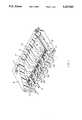
- FIG. 1is a partially cut-away, perspective view of an embodiment of the present invention.
- FIG. 2is a partially cut-away, perspective view of a modification of the embodiment shown in FIG. 1.
- a rectangular semiconductor chip 10has a plurality of chip terminals 11 arranged linearly along one of longer sides thereof.
- a main surface of the chip 10 except a portion thereof on which the chip terminals 11 are formedis covered by an insulating film 12 on which a plurality of leads 13 and 13a extending perpendicularly to the longer sides of the chip are arranged.
- the leads 13 and 13aare practically formed as a portion of a lead frame although they are shown schematically.
- Inner end portions of the respective lead fingers 13 and 13aare arranged in an area of the insulating sheet 12 in which the chip terminals 11 are arranged, and connected to the chip terminals 11 by bonding wires 14, respectively.
- Outer end portions of the lead fingers 13 and 13aextend to a terminal portion 15 through downward and outward bent portions accommodating to a surface mounting of the IC package onto a printed circuit board (not shown).
- the assemblyAfter bonding, the assembly is air-tightly sealed by a resin layer 16, resulting in an IC package.
- the lead fingers 13 and 13aare integral by tie-bars 17, respectively, and are separated by removing the tie-bars 17 immediately before the sealing step.
- FIG. 2which shows a modification of the embodiment shown in FIG. 1 and in which common constitutional elements to those of the embodiment shown in FIG. 1 are depicted by the same reference numerals, respectively, a portion of the chip terminals, that is, a chip terminal 11A is arranged in the vicinity of not the long side of the chip 10 but a short side thereof.
- An inner end portion of a portion of the lead fingers 13, that is, a lead finger 13bis arranged in the vicinity of the chip terminal 11A, correspondingly.
- the number of the chip terminals 11Amay be increased when the number of the chip terminals 11 is increased according to the integration density of internal circuits of the chip 10 required, so that distance between adjacent chip terminals can be maintained optimum.
- the number of the lead fingers 13bis also changeable suitably according to the number of the terminals 11A.
- the IC package structure according to the present inventionis suitable for miniaturization of package size and suitable to obtain a desired mechanical strength of the portion for mounting the lead fingers. Further, due to the shortened metal wires, the possibility of short-circuit and/or breakage of them is substantially reduced, resulting in an improved reliability of the IC package.
Landscapes
- Engineering & Computer Science (AREA)
- Computer Hardware Design (AREA)
- Microelectronics & Electronic Packaging (AREA)
- Power Engineering (AREA)
- Physics & Mathematics (AREA)
- Condensed Matter Physics & Semiconductors (AREA)
- General Physics & Mathematics (AREA)
- Wire Bonding (AREA)
- Semiconductor Integrated Circuits (AREA)
- Lead Frames For Integrated Circuits (AREA)
Abstract
Description
Claims (6)
Applications Claiming Priority (2)
| Application Number | Priority Date | Filing Date | Title |
|---|---|---|---|
| JP4130319AJPH0637136A (en) | 1992-05-22 | 1992-05-22 | Semiconductor device |
| JP4-130319 | 1992-05-22 |
Publications (1)
| Publication Number | Publication Date |
|---|---|
| US5327009Atrue US5327009A (en) | 1994-07-05 |
Family
ID=15031492
Family Applications (1)
| Application Number | Title | Priority Date | Filing Date |
|---|---|---|---|
| US08/064,980Expired - LifetimeUS5327009A (en) | 1992-05-22 | 1993-05-24 | Miniaturized integrated circuit package |
Country Status (2)
| Country | Link |
|---|---|
| US (1) | US5327009A (en) |
| JP (1) | JPH0637136A (en) |
Cited By (15)
| Publication number | Priority date | Publication date | Assignee | Title |
|---|---|---|---|---|
| US5793099A (en)* | 1988-09-20 | 1998-08-11 | Hitachi, Ltd. | Semiconductor device |
| US5808356A (en)* | 1996-04-16 | 1998-09-15 | Nec Corporation | Lead-frame having unused input/output terminals separated from input/output terminals connected to input/output strip lines |
| USRE36077E (en)* | 1991-10-15 | 1999-02-02 | Mitsubishi Denki Kabushiki Kaisha | Method of manufacturing inversion type IC's and IC module using same |
| US5903443A (en)* | 1997-04-07 | 1999-05-11 | Micron Technology, Inc. | Interdigitated leads-over-chip lead frame, device, and method for supporting an integrated circuit die |
| US6008996A (en)* | 1997-04-07 | 1999-12-28 | Micron Technology, Inc. | Interdigitated leads-over-chip lead frame, device, and method for supporting an integrated circuit die |
| US6052289A (en)* | 1998-08-26 | 2000-04-18 | Micron Technology, Inc. | Interdigitated leads-over-chip lead frame for supporting an integrated circuit die |
| US6144089A (en)* | 1997-11-26 | 2000-11-07 | Micron Technology, Inc. | Inner-digitized bond fingers on bus bars of semiconductor device package |
| US6268652B1 (en)* | 1997-09-26 | 2001-07-31 | Nec Corporation | CSP type semiconductor device with reduced package size |
| USD461172S1 (en) | 2001-07-17 | 2002-08-06 | Gem Services, Inc. | Surface mount package |
| US20040080056A1 (en)* | 2001-03-30 | 2004-04-29 | Lim David Chong Sook | Packaging system for die-up connection of a die-down oriented integrated circuit |
| US20050145998A1 (en)* | 2001-05-15 | 2005-07-07 | Gem Services, Inc. | Surface mount package |
| US20050236698A1 (en)* | 2004-04-27 | 2005-10-27 | Isao Ozawa | Semiconductor device in which semiconductor chip is mounted on lead frame |
| US20050245062A1 (en)* | 2004-04-29 | 2005-11-03 | Jeff Kingsbury | Single row bond pad arrangement |
| US20070069343A1 (en)* | 2005-09-26 | 2007-03-29 | Mitsubishi Denki Kabushiki Kaisha | Molded semiconductor package |
| US20160211200A1 (en)* | 2015-01-16 | 2016-07-21 | New Japan Radio Co., Ltd. | Semiconductor device |
Citations (7)
| Publication number | Priority date | Publication date | Assignee | Title |
|---|---|---|---|---|
| JPS5512791A (en)* | 1978-07-14 | 1980-01-29 | Nec Corp | Semiconductor device |
| US4825280A (en)* | 1986-10-01 | 1989-04-25 | Texas Instruments Incorporated | Electrostatic discharge protection for semiconductor devices |
| JPH01123427A (en)* | 1987-11-06 | 1989-05-16 | Mitsubishi Electric Corp | Resin-sealed semiconductor device |
| US4862245A (en)* | 1985-04-18 | 1989-08-29 | International Business Machines Corporation | Package semiconductor chip |
| JPH03256352A (en)* | 1990-03-06 | 1991-11-15 | Nec Corp | Semiconductor device |
| US5072280A (en)* | 1989-10-23 | 1991-12-10 | Nec Corporation | Resin sealed semiconductor device |
| US5233221A (en)* | 1990-10-24 | 1993-08-03 | International Business Machines Corporation | Electronic substrate multiple location conductor attachment technology |
- 1992
- 1992-05-22JPJP4130319Apatent/JPH0637136A/ennot_activeWithdrawn
- 1993
- 1993-05-24USUS08/064,980patent/US5327009A/ennot_activeExpired - Lifetime
Patent Citations (7)
| Publication number | Priority date | Publication date | Assignee | Title |
|---|---|---|---|---|
| JPS5512791A (en)* | 1978-07-14 | 1980-01-29 | Nec Corp | Semiconductor device |
| US4862245A (en)* | 1985-04-18 | 1989-08-29 | International Business Machines Corporation | Package semiconductor chip |
| US4825280A (en)* | 1986-10-01 | 1989-04-25 | Texas Instruments Incorporated | Electrostatic discharge protection for semiconductor devices |
| JPH01123427A (en)* | 1987-11-06 | 1989-05-16 | Mitsubishi Electric Corp | Resin-sealed semiconductor device |
| US5072280A (en)* | 1989-10-23 | 1991-12-10 | Nec Corporation | Resin sealed semiconductor device |
| JPH03256352A (en)* | 1990-03-06 | 1991-11-15 | Nec Corp | Semiconductor device |
| US5233221A (en)* | 1990-10-24 | 1993-08-03 | International Business Machines Corporation | Electronic substrate multiple location conductor attachment technology |
Non-Patent Citations (2)
| Title |
|---|
| W. Ward, "Volume Production of Unique . . . IBM 80-ns 1-Mbit DRAM Chip by Area Wire Bond Techniques", Proceedings of the 38th Electronic Component Conference, XIII-4, May, 1988, pp. 552-557. |
| W. Ward, Volume Production of Unique . . . IBM 80 ns 1 Mbit DRAM Chip by Area Wire Bond Techniques , Proceedings of the 38th Electronic Component Conference, XIII 4, May, 1988, pp. 552 557.* |
Cited By (44)
| Publication number | Priority date | Publication date | Assignee | Title |
|---|---|---|---|---|
| US6072231A (en)* | 1988-03-20 | 2000-06-06 | Hitachi, Ltd. | Semiconductor device |
| US6130114A (en)* | 1988-03-20 | 2000-10-10 | Hitachi, Ltd. | Semiconductor device |
| US6081023A (en)* | 1988-03-20 | 2000-06-27 | Hitachi, Ltd. | Semiconductor device |
| US6919622B2 (en) | 1988-09-20 | 2005-07-19 | Renesas Technology Corp. | Semiconductor device |
| US5914530A (en)* | 1988-09-20 | 1999-06-22 | Hitachi, Ltd. | Semiconductor device |
| US5793099A (en)* | 1988-09-20 | 1998-08-11 | Hitachi, Ltd. | Semiconductor device |
| US20040155323A1 (en)* | 1988-09-20 | 2004-08-12 | Gen Murakami | Semiconductor device |
| US6720208B2 (en) | 1988-09-20 | 2004-04-13 | Renesas Technology Corporation | Semiconductor device |
| US6018191A (en)* | 1988-09-20 | 2000-01-25 | Hitachi, Ltd. | Semiconductor device |
| US6531760B1 (en) | 1988-09-20 | 2003-03-11 | Gen Murakami | Semiconductor device |
| US6069029A (en)* | 1988-09-20 | 2000-05-30 | Hitachi, Ltd. | Semiconductor device chip on lead and lead on chip manufacturing |
| US5863817A (en)* | 1988-09-20 | 1999-01-26 | Hitachi, Ltd. | Semiconductor device |
| US6303982B2 (en) | 1988-09-20 | 2001-10-16 | Hitachi, Ltd. | Semiconductor device |
| USRE36077E (en)* | 1991-10-15 | 1999-02-02 | Mitsubishi Denki Kabushiki Kaisha | Method of manufacturing inversion type IC's and IC module using same |
| US5808356A (en)* | 1996-04-16 | 1998-09-15 | Nec Corporation | Lead-frame having unused input/output terminals separated from input/output terminals connected to input/output strip lines |
| US6107677A (en)* | 1997-04-07 | 2000-08-22 | Micron Technology, Inc. | Interdigitated leads-over-chip lead frame, device, and method for supporting an integrated circuit die |
| US5977616A (en)* | 1997-04-07 | 1999-11-02 | Micron Technology, Inc. | Interdigitated leads-over-chip lead frame, device, and method for supporting an integrated circuit die |
| US6148509A (en)* | 1997-04-07 | 2000-11-21 | Micron Technology, Inc. | Method for supporting an integrated circuit die |
| US5973935A (en)* | 1997-04-07 | 1999-10-26 | Micron Technology, Inc. | Interdigitated leads-over-chip lead frame for supporting an integrated circuit die |
| US6271582B1 (en)* | 1997-04-07 | 2001-08-07 | Micron Technology, Inc. | Interdigitated leads-over-chip lead frame, device, and method for supporting an integrated circuit die |
| US6576987B2 (en) | 1997-04-07 | 2003-06-10 | Micron Technology, Inc. | Interdigitated leads-over-chip lead frame, device, and method for supporting an integrated circuit die |
| US6344976B1 (en) | 1997-04-07 | 2002-02-05 | Micron Technology, Inc. | Interdigitated leads-over-chip lead frame device and method for supporting an integrated circuit die |
| US6831353B2 (en) | 1997-04-07 | 2004-12-14 | Micron Technology, Inc. | Interdigitated leads-over-chip lead frame and device for supporting an integrated circuit die |
| US5903443A (en)* | 1997-04-07 | 1999-05-11 | Micron Technology, Inc. | Interdigitated leads-over-chip lead frame, device, and method for supporting an integrated circuit die |
| US6008996A (en)* | 1997-04-07 | 1999-12-28 | Micron Technology, Inc. | Interdigitated leads-over-chip lead frame, device, and method for supporting an integrated circuit die |
| US20030193081A1 (en)* | 1997-04-07 | 2003-10-16 | Aaron Schoenfeld | Interdigitated leads-over-chip lead frame and device for supporting an integrated circuit die |
| US6268652B1 (en)* | 1997-09-26 | 2001-07-31 | Nec Corporation | CSP type semiconductor device with reduced package size |
| US6630732B2 (en) | 1997-11-26 | 2003-10-07 | Micron Technology, Inc. | Lead frames including inner-digitized bond fingers on bus bars and semiconductor device package including same |
| US6144089A (en)* | 1997-11-26 | 2000-11-07 | Micron Technology, Inc. | Inner-digitized bond fingers on bus bars of semiconductor device package |
| US6376282B1 (en) | 1997-11-26 | 2002-04-23 | Micron Technology, Inc. | Inner-digitized bond fingers on bus bars of semiconductor device package |
| US6052289A (en)* | 1998-08-26 | 2000-04-18 | Micron Technology, Inc. | Interdigitated leads-over-chip lead frame for supporting an integrated circuit die |
| US20040080056A1 (en)* | 2001-03-30 | 2004-04-29 | Lim David Chong Sook | Packaging system for die-up connection of a die-down oriented integrated circuit |
| US20070007640A1 (en)* | 2001-05-15 | 2007-01-11 | Gem Services, Inc. | Surface mount package |
| US20050145998A1 (en)* | 2001-05-15 | 2005-07-07 | Gem Services, Inc. | Surface mount package |
| US7057273B2 (en) | 2001-05-15 | 2006-06-06 | Gem Services, Inc. | Surface mount package |
| USD461172S1 (en) | 2001-07-17 | 2002-08-06 | Gem Services, Inc. | Surface mount package |
| US20050236698A1 (en)* | 2004-04-27 | 2005-10-27 | Isao Ozawa | Semiconductor device in which semiconductor chip is mounted on lead frame |
| US7339257B2 (en)* | 2004-04-27 | 2008-03-04 | Kabushiki Kaisha Toshiba | Semiconductor device in which semiconductor chip is mounted on lead frame |
| US20050245062A1 (en)* | 2004-04-29 | 2005-11-03 | Jeff Kingsbury | Single row bond pad arrangement |
| WO2005112115A1 (en)* | 2004-04-29 | 2005-11-24 | Jeff Kingsbury | Single row bond pad arrangement of an integrated circuit chip |
| US20070069343A1 (en)* | 2005-09-26 | 2007-03-29 | Mitsubishi Denki Kabushiki Kaisha | Molded semiconductor package |
| US7414300B2 (en)* | 2005-09-26 | 2008-08-19 | Mitsubishi Denki Kabushiki Kaisha | Molded semiconductor package |
| US20160211200A1 (en)* | 2015-01-16 | 2016-07-21 | New Japan Radio Co., Ltd. | Semiconductor device |
| US9666509B2 (en)* | 2015-01-16 | 2017-05-30 | New Japan Radio Co., Ltd. | Semiconductor device |
Also Published As
| Publication number | Publication date |
|---|---|
| JPH0637136A (en) | 1994-02-10 |
Similar Documents
| Publication | Publication Date | Title |
|---|---|---|
| US5800958A (en) | Electrically enhanced power quad flat pack arrangement | |
| US6303997B1 (en) | Thin, stackable semiconductor packages | |
| US5939779A (en) | Bottom lead semiconductor chip stack package | |
| US6781240B2 (en) | Semiconductor package with semiconductor chips stacked therein and method of making the package | |
| US5563446A (en) | Surface mount peripheral leaded and ball grid array package | |
| US6504236B2 (en) | Semiconductor die assembly having leadframe decoupling characters and method | |
| US6731015B2 (en) | Super low profile package with stacked dies | |
| US4989068A (en) | Semiconductor device and method of manufacturing the same | |
| US5327009A (en) | Miniaturized integrated circuit package | |
| US5252854A (en) | Semiconductor device having stacked lead structure | |
| JP2509027B2 (en) | Semiconductor device | |
| KR100369907B1 (en) | Semiconductor Package And Mounting Structure On Substrate Thereof And Stack Structure Thereof | |
| US20010030357A1 (en) | Semiconductor apparatus substrate, semiconductor apparatus, and method of manufacturing thereof and electronic apparatus | |
| US20040188818A1 (en) | Multi-chips module package | |
| CN1114948C (en) | Semiconductor chip package having combined structure of lead-on-chip leads and standard normal leads | |
| JP2524482B2 (en) | QFP structure semiconductor device | |
| US7492038B2 (en) | Semiconductor device | |
| JP3132478B2 (en) | Semiconductor device and method of manufacturing the same | |
| JP2972486B2 (en) | Semiconductor device | |
| KR0129198B1 (en) | Semiconductor package | |
| KR950013049B1 (en) | Multi chip loc package | |
| KR950008240B1 (en) | Semiconductor package | |
| JP2963548B2 (en) | Semiconductor device | |
| KR100206975B1 (en) | Semiconductor package | |
| KR100273269B1 (en) | Semiconductor cob module and method for fabricating the same |
Legal Events
| Date | Code | Title | Description |
|---|---|---|---|
| AS | Assignment | Owner name:NEC CORPORATION, JAPAN Free format text:ASSIGNMENT OF ASSIGNORS INTEREST;ASSIGNOR:IGETA, MASAHIKO;REEL/FRAME:006582/0230 Effective date:19930519 | |
| STPP | Information on status: patent application and granting procedure in general | Free format text:APPLICATION UNDERGOING PREEXAM PROCESSING | |
| CC | Certificate of correction | ||
| FEPP | Fee payment procedure | Free format text:PAYOR NUMBER ASSIGNED (ORIGINAL EVENT CODE: ASPN); ENTITY STATUS OF PATENT OWNER: LARGE ENTITY | |
| FEPP | Fee payment procedure | Free format text:PAYOR NUMBER ASSIGNED (ORIGINAL EVENT CODE: ASPN); ENTITY STATUS OF PATENT OWNER: LARGE ENTITY Free format text:PAYER NUMBER DE-ASSIGNED (ORIGINAL EVENT CODE: RMPN); ENTITY STATUS OF PATENT OWNER: LARGE ENTITY | |
| FPAY | Fee payment | Year of fee payment:4 | |
| FPAY | Fee payment | Year of fee payment:8 | |
| AS | Assignment | Owner name:NEC ELECTRONICS CORPORATION, JAPAN Free format text:ASSIGNMENT OF ASSIGNORS INTEREST;ASSIGNOR:NEC CORPORATION;REEL/FRAME:013758/0595 Effective date:20030110 | |
| FPAY | Fee payment | Year of fee payment:12 | |
| AS | Assignment | Owner name:ELPIDA MEMORY, INC., JAPAN Free format text:ASSIGNMENT OF ASSIGNORS INTEREST;ASSIGNORS:NEC CORPORATION;NEC ELECTRONICS CORPORATION;REEL/FRAME:018545/0737 Effective date:20060531 | |
| AS | Assignment | Owner name:APPLE INC., CALIFORNIA Free format text:SECURITY AGREEMENT;ASSIGNOR:ELPIDA MEMORY, INC.;REEL/FRAME:028209/0477 Effective date:20120410 | |
| AS | Assignment | Owner name:ELPIDA MEMORY, INC., JAPAN Free format text:RELEASE BY SECURED PARTY;ASSIGNOR:APPLE, INC;REEL/FRAME:032277/0661 Effective date:20140114 |